Control of the Nucleation Density of Molybdenum Disulfide in Large-Scale Synthesis Using Chemical Vapor Deposition

Abstract
1. Introduction
2. Materials and Methods
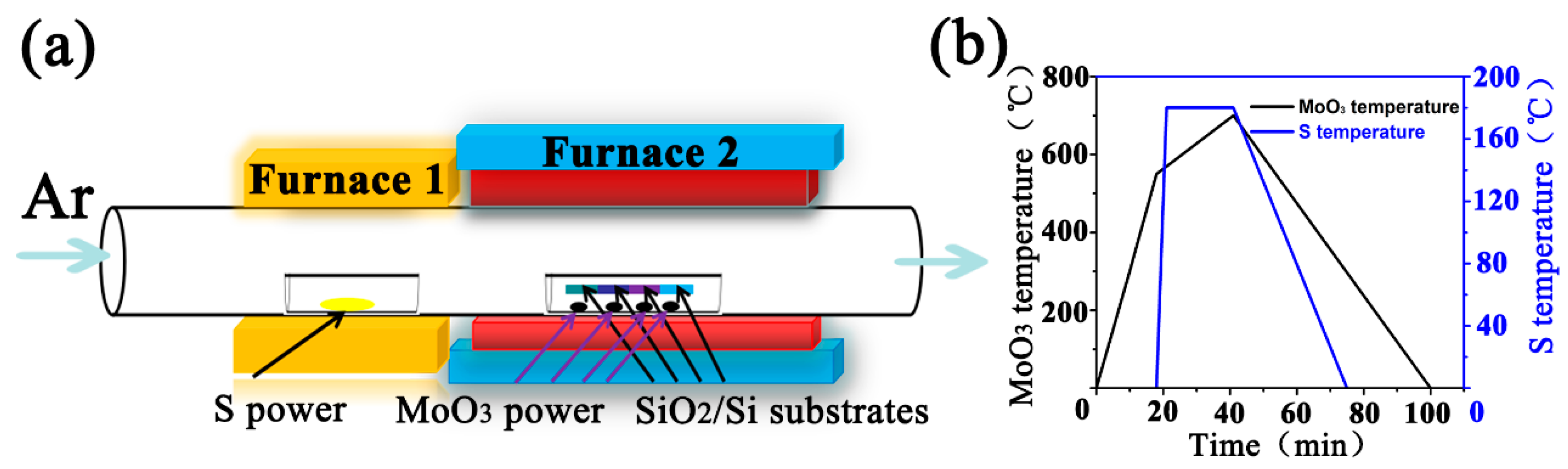
2.1. Synthesis Precursor
2.2. Synthesis Procedure
2.3. Characterizations
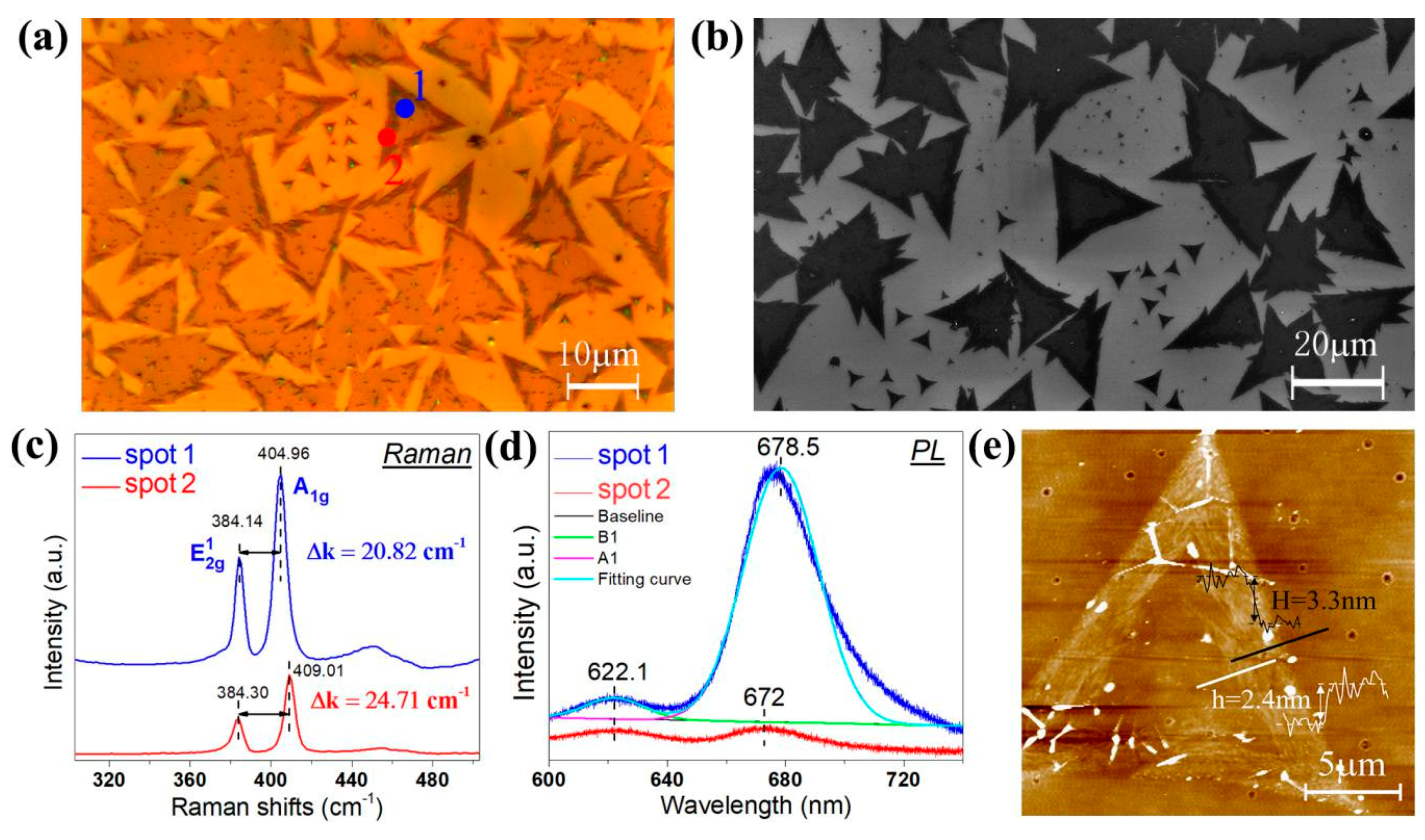
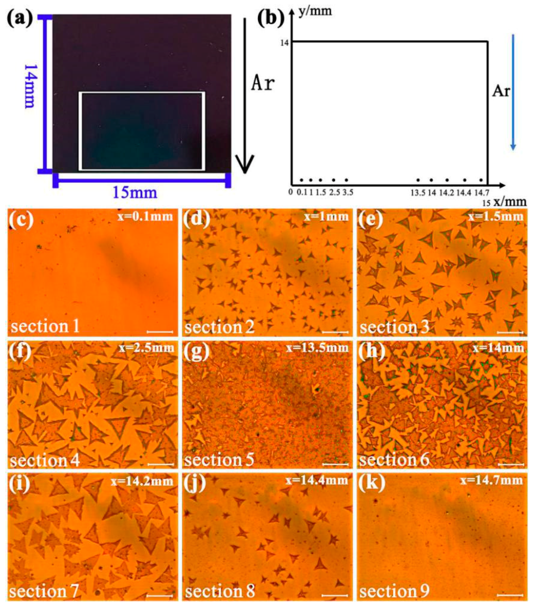
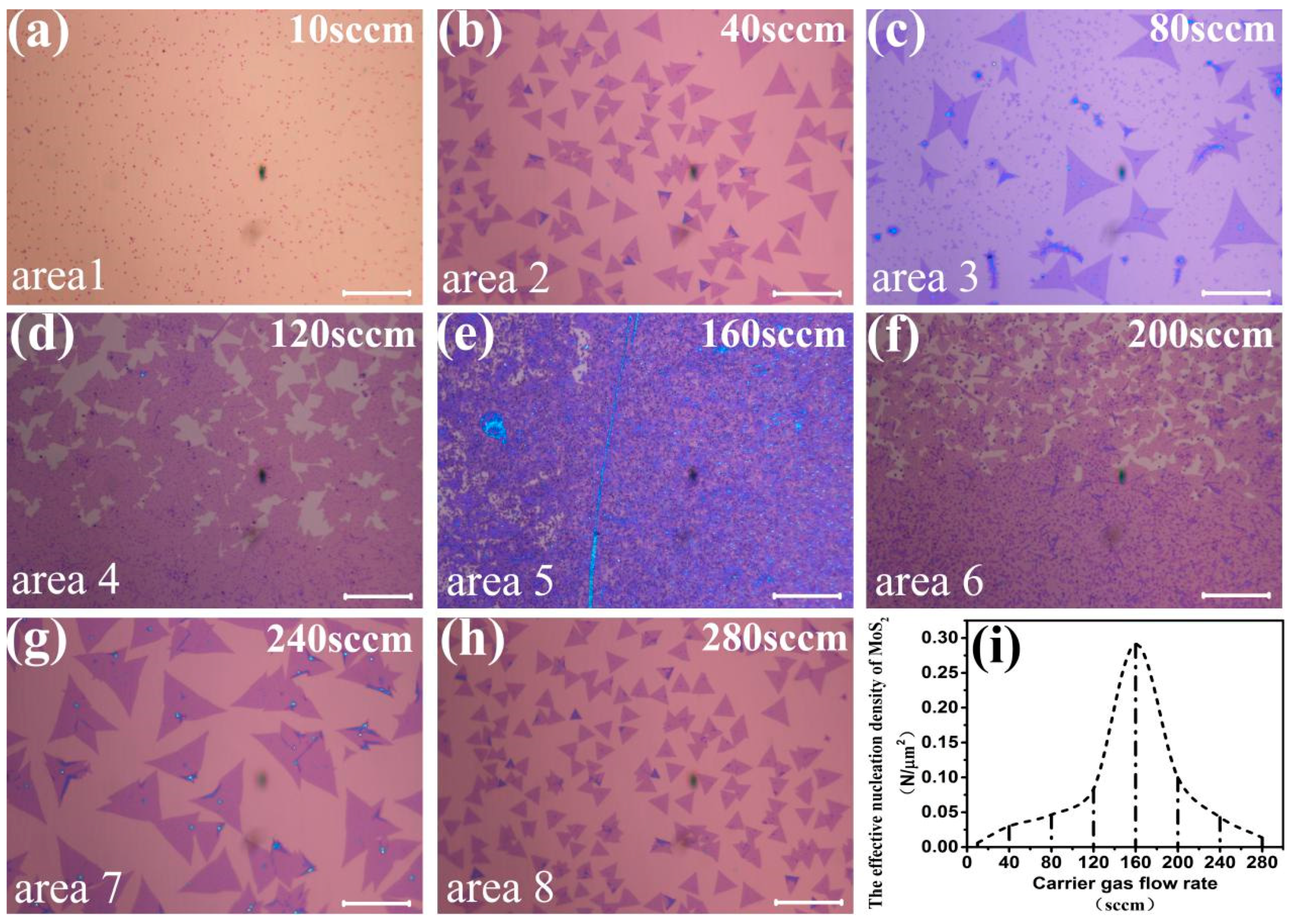
3. Results and Discussion
4. Conclusions
Author Contributions
Funding
Conflicts of Interest
References
- Liu, L.; Liu, Z.; Huang, P.; Wu, Z.; Jiang, S. Protein-induced ultrathin molybdenum disulfide (MoS2) flakes for a water-based lubricating system. RSC Adv. 2016, 6. [Google Scholar] [CrossRef]
- Zhan, Y.; Liu, Z.; Najmaei, S.; Ajayan, P.M.; Lou, J. Large Area Vapor Phase Growth and Characterization of MoS2 Atomic Layers on SiO2 Substrate. Small 2012, 8, 966. [Google Scholar] [CrossRef] [PubMed]
- Island, J.O.; MolinaMendoza, A.J.; Barawi, M.; Biele, R.; Flores, E.; Clamagirand, J.M.; Ares, J.R.; Sanchez, C.; van der Zant, H.S.J.; D’Agosta, R.; et al. Electronics and optoelectronics of quasi-one dimensional layered transition metal trichalcogenides. 2D Mater. 2017, 4. [Google Scholar] [CrossRef]
- Amani, M.; Chin, M.L.; Birdwell, A.G.; O’Regan, T.P.; Najmaei, S.; Liu, Z.; Ajayan, P.M.; Lou, J.; Dubey, M. Electrical performance of monolayer MoS2 field-effect transistors prepared by chemical vapor deposition. Appl. Phys. Lett. 2013, 102, 136805. [Google Scholar] [CrossRef]
- Lee, H.S.; Kim, M.S.; Jin, Y.; Han, G.H.; Lee, Y.H.; Kim, J. Efficient Exciton–Plasmon Conversion in Ag Nanowire/Monolayer MoS2 Hybrids: Direct Imaging and Quantitative Estimation of Plasmon Coupling and Propagation. Adv. Opt. Mater. 2015, 3, 943–947. [Google Scholar] [CrossRef]
- Radisavljevic, B.; Radenovic, A.; Brivio, J.; Giacometti, V.; Kis, A. Single-layer MoS2 transistors. Nat. Nanotechnol. 2011, 6, 147–150. [Google Scholar] [CrossRef] [PubMed]
- Cho, K.; Pak, J.; Kim, J.K.; Kang, K.; Kim, T.Y.; Shin, J.; Choi, B.Y.; Chung, S.; Lee, T. Contact-Engineered Electrical Properties of MoS2 Field-Effect Transistors via Selectively Deposited Thiol-Molecules. Adv. Mater. 2018, e1705540. [Google Scholar] [CrossRef] [PubMed]
- Zhang, W.; Huang, J.K.; Chen, C.H.; Chang, Y.H.; Cheng, Y.J.; Li, L.J. High-Gain Phototransistors Based on a CVD MoS2 Monolayer. Adv. Mater. 2013, 25, 3456–3461. [Google Scholar] [CrossRef] [PubMed]
- Xu, H.; Han, X.; Dai, X.; Liu, W.; Wu, J.; Zhu, J.; Kim, D.; Zou, G.; Sablon, K.A.; Sergeev, A.; et al. High Detectivity and Transparent Few-Layer MoS2/Glassy-Graphene Heterostructure Photodetectors. Adv. Mater. 2018, 30, e1706561. [Google Scholar] [CrossRef] [PubMed]
- Sundaram, R.S.; Engel, M.; Lombardo, A.; Krupke, R.; Ferrari, A.C.; Avouris, P.; Steiner, M. Electroluminescence in single layer MoS2. Nano Lett. 2013, 13, 1416. [Google Scholar] [CrossRef] [PubMed]
- Choi, G.J.; Van, L.Q.; Choi, K.S.; Kwon, K.C.; Jang, H.W.; Gwag, J.S.; Kim, S.Y. Polarized Light-Emitting Diodes Based on Patterned MoS2 Nanosheet Hole Transport Layer. Adv. Mater. 2017, 29, 1702598. [Google Scholar] [CrossRef] [PubMed]
- Tsai, M.L.; Su, S.H.; Chang, J.K.; Tsai, D.S.; Chen, C.H.; Wu, C.I.; Li, L.J.; Chen, L.J.; He, J.H. Monolayer MoS2 heterojunction solar cells. ACS Nano 2014, 8, 8317–8322. [Google Scholar] [CrossRef] [PubMed]
- Singh, E.; Kim, K.S.; Yeom, G.Y.; Nalwa, H.S. Atomically Thin-Layered Molybdenum Disulfide (MoS2) for Bulk-Heterojunction Solar Cells. ACS Appl. Mater. Interfaces 2017, 9, 3223. [Google Scholar] [CrossRef] [PubMed]
- Li, H.; Yin, Z.; He, Q.; Li, H.; Huang, X.; Lu, G.; Fam, D.W.H.; Tok, A.I.Y.; Zhang, Q.; Zhang, H. Layered Nanomaterials: Fabrication of Single-and Multilayer MoS2 Film-Based Field-Effect Transistors for Sensing NO at Room Temperature (Small 1/2012). Small 2012, 8, 2. [Google Scholar] [CrossRef]
- Zheng, J.; Yan, X.; Lu, Z.; Qiu, H.; Xu, G.; Zhou, X.; Wang, P.; Pan, X.; Liu, K.; Jiao, L. High-Mobility Multilayered MoS2 Flakes with Low Contact Resistance Grown by Chemical Vapor Deposition. Adv. Mater. 2017, 29, 1604540. [Google Scholar] [CrossRef] [PubMed]
- Li, X.L.; Prof, Y.D.L. Formation of MoS2 Inorganic Fullerenes (IFs) by the Reaction of MoO3 Nanobelts and S. Chem. Eur. J. 2003, 9, 2726–2731. [Google Scholar] [CrossRef] [PubMed]
- Lee, Y.H.; Yu, L.; Wang, H.; Fang, W.; Ling, X.; Shi, Y.; Lin, C.T.; Huang, J.K.; Chang, M.T.; Chang, C.S.; et al. Synthesis and Transfer of Single-Layer Transition Metal Disulfides on Diverse Surfaces. Nano Lett. 2013, 13, 1852. [Google Scholar] [CrossRef] [PubMed]
- Gong, C.; Huang, C.; Miller, J.; Cheng, L.; Hao, Y.; Cobden, D.; Kim, J.; Ruoff, R.S.; Wallace, R.M.; Cho, K.; et al. Metal Contacts on Physical Vapor Deposited Monolayer MoS2. ACS Nano 2013, 7, 11350–11357. [Google Scholar] [CrossRef] [PubMed]
- Wang, S.; Pacios, M.; Bhaskaran, H.; Warner, J.H. Substrate control for large area continuous films of monolayer MoS2 by atmospheric pressure chemical vapor deposition. Nanotechnology 2016, 27, 085604. [Google Scholar] [CrossRef] [PubMed]
- Ling, X.; Lee, Y.H.; Lin, Y.; Fang, W.; Yu, L.; Dresselhaus, M.S.; Kong, J. Role of the Seeding Promoter in MoS2 Growth by Chemical Vapor Deposition. Nano Lett. 2014, 14, 464. [Google Scholar] [CrossRef] [PubMed]
- Njiwa, P.; Aurélie, H.A.; Afanasiev, P.; Geantet, C.; Bosselet, F.; Vacher, B.; Thierry Le Mogne, M.B.; Dassenoy, F. Tribological Properties of New MoS2, Nanoparticles Prepared by Seed-Assisted Solution Technique. Tribol. Lett. 2014, 55, 473–481. [Google Scholar] [CrossRef]
- Kim, H.; Ovchinnikov, D.; Deiana, D.; Unuchek, D.; Kis, A. Suppressing nucleation in metalorganic chemical vapor deposition of MoS2 monolayers by alkali metal halides. Nano Lett. 2017. [Google Scholar] [CrossRef] [PubMed]
- Late, D.J.; Liu, B.; Matte, H.S.S.R.; Rao, C.N.R.; Dravid, V.P. Rapid Characterization of Ultrathin Layers of Chalcogenides on SiO2/Si Substrates. Adv. Funct. Mater. 2012, 22, 1894–1905. [Google Scholar] [CrossRef]
- Splendiani, A.; Sun, L.; Zhang, Y.; Li, T.; Kim, J.; Chim, C.Y.; Galli, G.; Wang, F. Emerging Photoluminescence in Monolayer MoS2. Nano Lett. 2010, 10, 1271–1275. [Google Scholar] [CrossRef] [PubMed]
- Lee, Y.H.; Zhang, X.Q.; Zhang, W.; Chang, M.T.; Lin, C.T.; Chang, K.D.; Yu, Y.C.; Wang, J.T.; Chang, C.S.; Li, L.J.; et al. Synthesis of large-area MoS2 atomic layers with chemical vapor deposition. Adv. Mater. 2012, 24, 2320–2325. [Google Scholar] [CrossRef] [PubMed]
- Yu, Y.; Li, C.; Liu, Y.; Su, L.; Zhang, Y.; Cao, L. Controlled scalable synthesis of uniform, high-quality monolayer and few-layer MoS2 films. J. Sci. Rep. 2013, 3, 1866. [Google Scholar] [CrossRef] [PubMed]
- Wang, S.; Rong, Y.; Fan, Y.; Pacios, M.; Bhaskaran, H.; He, K.; Warner, J.H. Shape Evolution of Monolayer MoS2 Crystals Grown by Chemical Vapor Deposition. Chem. Mater. 2014, 26. [Google Scholar] [CrossRef]
- Govind, R.A.; Warner, J.H.; Blankschtein, D.; Strano, M.S.A. Generalized Mechanistic Model for the Chemical Vapor Deposition of 2D Transition Metal Dichalcogenide Monolayers. ACS Nano 2016, 10, 4330. [Google Scholar] [CrossRef] [PubMed]
- Incropera, F.P. Fundamentals of Heat and Mass Transfer; John Wiley & Sons: Hoboken, NJ, USA, 2007. [Google Scholar]
- Stoica, T.; Stoica, M.; Duchamp, M.; Tiedemann, A.; Mantl, S.; Grützmacher, D.; Buca, D.; Kardynał, B.E. Vapor transport growth of MoS2, nucleated on SiO2, patterns and graphene flakes. Nano Res. 2016, 9, 3504–3514. [Google Scholar] [CrossRef]
- Chen, B.; Yu, Q.; Yang, Q.; Bao, P.; Zhang, W.; Lou, L.; Zhu, W.; Wang, G. Large-area high quality MoS2 monolayers grown by sulfur vapor counter flow diffusion. RSC Adv. 2016, 6, 50306–50314. [Google Scholar] [CrossRef]
- Cao, Y.; Luo, X.; Han, S.; Yuan, C.; Yang, Y.; Li, Q.; Yu, T.; Ye, S. Influences of carrier gas flow rate on the morphologies of MoS2, flakes. Chem. Phys. Lett. 2015, 631, 30–33. [Google Scholar] [CrossRef]


| Section | The Number of Effective Nucleation Points of MoS2 (N) | The Effective Nucleation Density of MoS2 (N/μm2) |
|---|---|---|
| Section 1 (Figure 3e) | 207 | 0.0103 |
| Section 2 (Figure 3f) | 336 | 0.0167 |
| Section 3 (Figure 3g) | 784 | 0.0389 |
| Section 4 (Figure 3h) | 608 | 0.0302 |
| Section 5 (Figure 3i) | 72 | 0.0036 |
© 2018 by the authors. Licensee MDPI, Basel, Switzerland. This article is an open access article distributed under the terms and conditions of the Creative Commons Attribution (CC BY) license (http://creativecommons.org/licenses/by/4.0/).
Share and Cite
Xu, H.; Zhou, W.; Zheng, X.; Huang, J.; Feng, X.; Ye, L.; Xu, G.; Lin, F. Control of the Nucleation Density of Molybdenum Disulfide in Large-Scale Synthesis Using Chemical Vapor Deposition. Materials 2018, 11, 870. https://doi.org/10.3390/ma11060870
Xu H, Zhou W, Zheng X, Huang J, Feng X, Ye L, Xu G, Lin F. Control of the Nucleation Density of Molybdenum Disulfide in Large-Scale Synthesis Using Chemical Vapor Deposition. Materials. 2018; 11(6):870. https://doi.org/10.3390/ma11060870
Chicago/Turabian StyleXu, Haitao, Weipeng Zhou, Xiaowu Zheng, Jiayao Huang, Xiliang Feng, Li Ye, Guanjin Xu, and Fang Lin. 2018. "Control of the Nucleation Density of Molybdenum Disulfide in Large-Scale Synthesis Using Chemical Vapor Deposition" Materials 11, no. 6: 870. https://doi.org/10.3390/ma11060870
APA StyleXu, H., Zhou, W., Zheng, X., Huang, J., Feng, X., Ye, L., Xu, G., & Lin, F. (2018). Control of the Nucleation Density of Molybdenum Disulfide in Large-Scale Synthesis Using Chemical Vapor Deposition. Materials, 11(6), 870. https://doi.org/10.3390/ma11060870