Optoelectronic Properties of X-Doped (X = O, S, Te) Photovoltaic CSe with Puckered Structure


Abstract
1. Introduction
2. Computational Models and Method
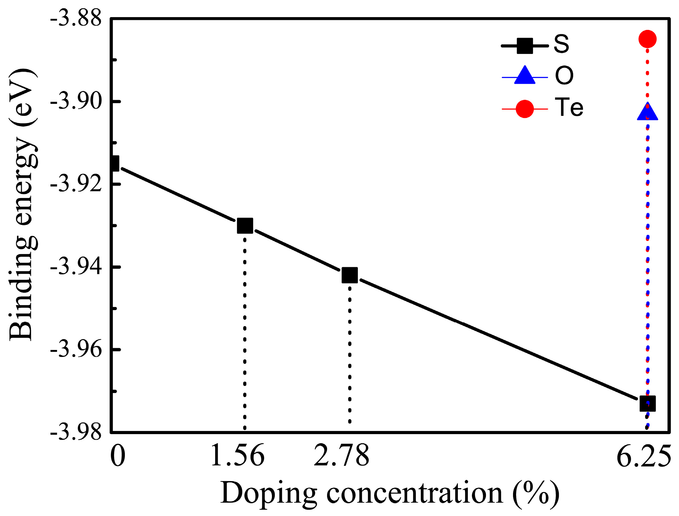
3. Results and Discussion
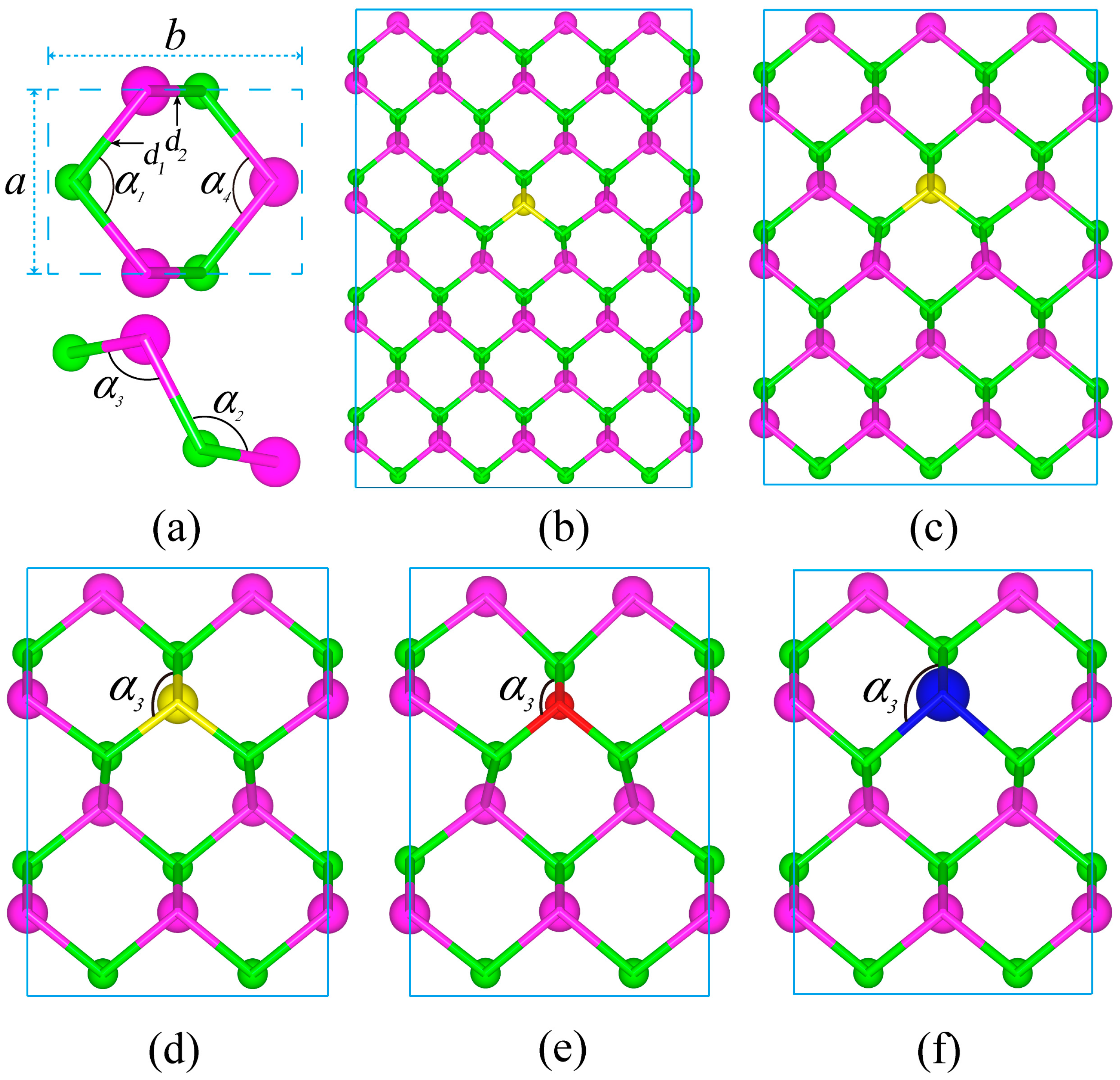
3.1. Geometric Structures
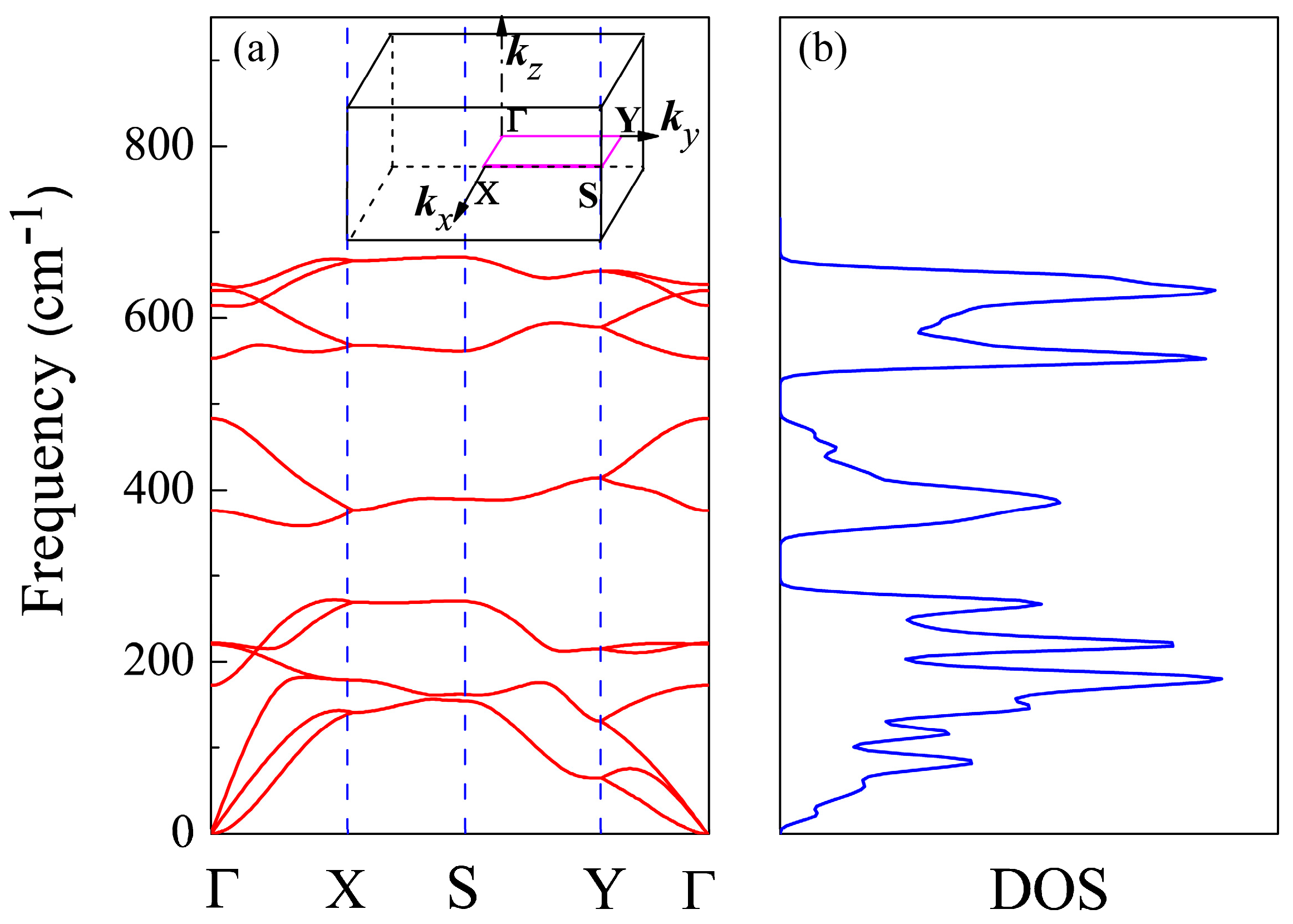
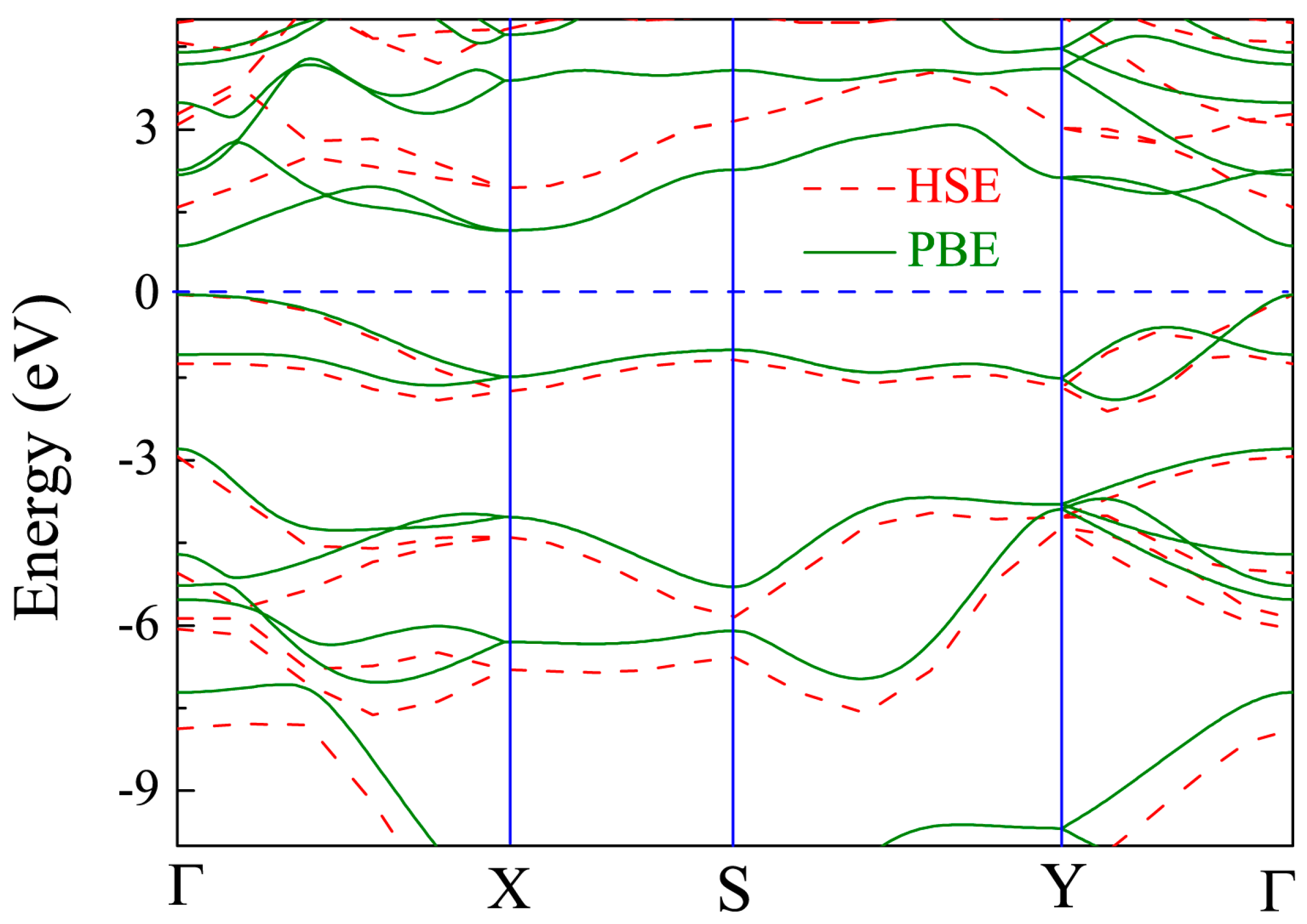
3.2. Electronic Structure
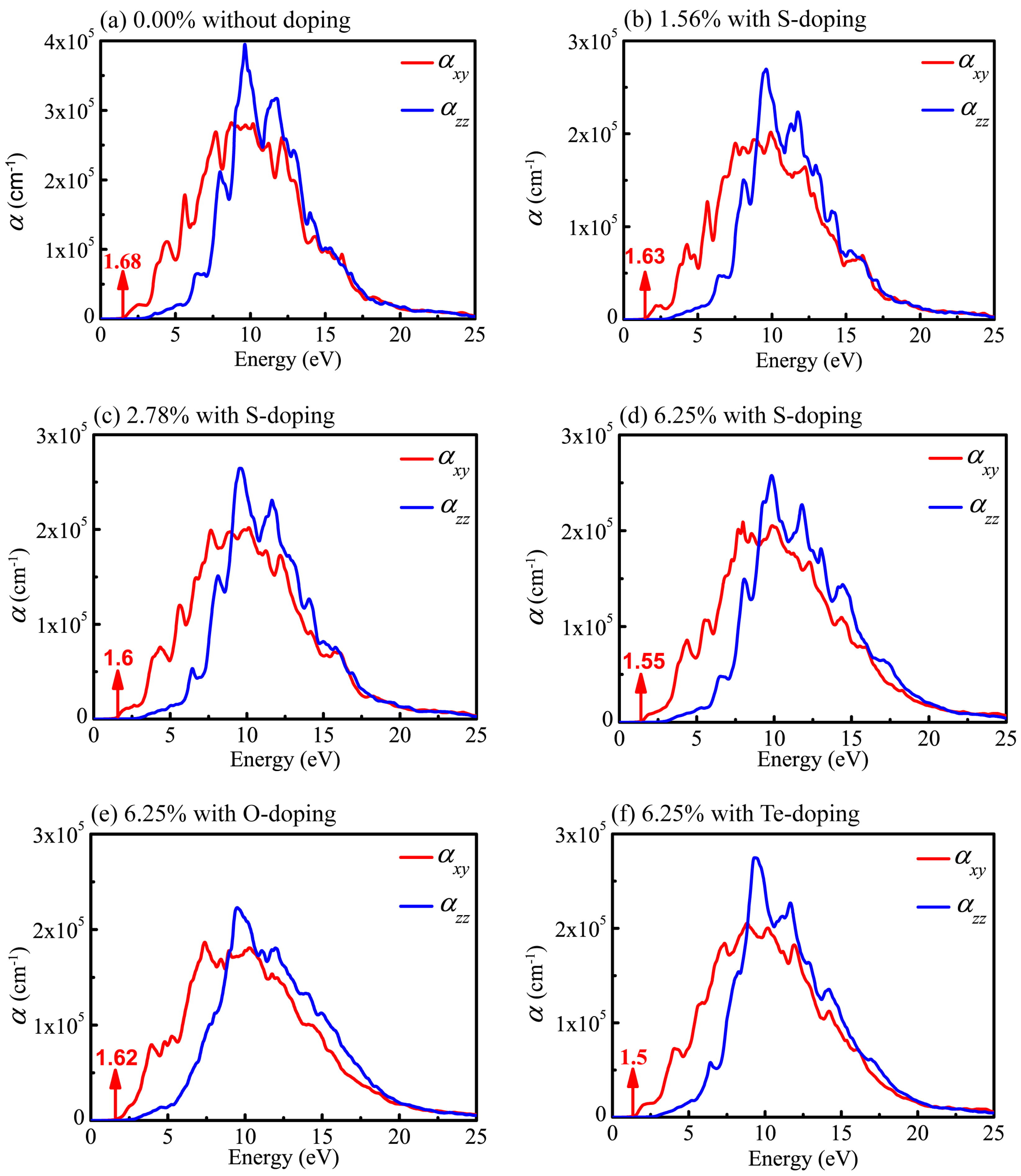
3.3. Optical Properties
4. Conclusions
Acknowledgments
Author Contributions
Conflicts of Interest
References
- Geim, A.K.; Novoselov, K.S. The rise of graphene. Nat. Mater. 2007, 6, 183–191. [Google Scholar] [CrossRef] [PubMed]
- Han, M.Y.; Ozyilmaz, B.; Zhang, Y.; Kim, P. Energy Band-Gap Engineering of Graphene Nanoribbons. Phys. Rev. Lett. 2007, 98, 206805. [Google Scholar] [CrossRef] [PubMed]
- Son, Y.W.; Cohen, M.L.; Louie, S.G. Energy Gaps in Graphene Nanoribbons. Phys. Rev. Lett. 2006, 97, 216803. [Google Scholar] [CrossRef] [PubMed]
- Minot, E.D.; Yaish, Y.; Sazonova, V.; Park, J.Y.; Brink, M.; McEuen, P.L. Tuning Carbon Nanotube Band Gaps with Strain. Phys. Rev. Lett. 2003, 90, 156401-1–156401-4. [Google Scholar] [CrossRef] [PubMed]
- Ouyang, M.; Huang, J.L.; Cheung, C.L.; Lieber, C.M. Energy Gaps in “Metallic” Single-Walled Carbon Nanotubes. Science 2001, 292, 702–705. [Google Scholar] [CrossRef] [PubMed]
- Zhang, Y.; Tang, T.T.; Girit, C.; Hao, Z.; Martin, M.C.; Zettl, A.; Crommie, M.F.; Shen, Y.R.; Wang, F. Direct observation of a widely tunable bandgap in bilayer graphene. Nature 2009, 459, 820–823. [Google Scholar] [CrossRef] [PubMed]
- Mak, K.F.; Lee, C.; Hone, J.; Shan, J.; Heinz, T.F. Atomically Thin MoS2: A New Direct-Gap Semiconductor. Phys. Rev. Lett. 2010, 105, 136805. [Google Scholar] [CrossRef] [PubMed]
- Splendiani, A.; Sun, L.; Zhang, Y.; Li, T.; Kim, J.; Chim, C.Y.; Galli, G.; Wang, F. Emerging Photoluminescence in Monolayer MoS2. Nano Lett. 2010, 10, 1271–1275. [Google Scholar] [CrossRef] [PubMed]
- Radisavljevic, B.; Radenovic, A.; Brivio, J.; Giacometti, V.; Kis, A. Single-layer MoS2 transistors. Nat. Nanotechnol. 2011, 6, 147–150. [Google Scholar] [CrossRef] [PubMed]
- Ghatak, S.; Ghosh, A. Observation of trap-assisted space charge limited conductivity in short channel MoS2 transistor. Appl. Phys. Lett. 2013, 103, 122103. [Google Scholar] [CrossRef]
- Guo, H.Y.; Lu, N.; Dai, J.; Wu, X.J.; Zeng, X.C. Phosphorene Nanoribbons, Phosphorus Nanotubes, and van der Waals Multilayers. J. Phys. Chem. C 2014, 118, 14051–14059. [Google Scholar] [CrossRef]
- Castellanos-Gomez, A. Black Phosphorus: Narrow Gap, Wide Applications. J. Phys. Chem. Lett. 2015, 6, 4280–4291. [Google Scholar] [CrossRef] [PubMed]
- Lu, J.; Carvalho, A.; Chan, X.K.; Liu, H.; Liu, B.; Tok, E.S.; Loh, K.P.; Castro Neto, A.H.; Sow, C.H. Atomic Healing of Defects in Transition Metal Dichalcogenides. Nano Lett. 2015, 15, 3524–3532. [Google Scholar] [CrossRef] [PubMed]
- Kang, J.; Tongay, S.; Zhou, J.; Li, J.; Wu, J. Band offsets and heterostructures of two-dimensional semiconductors. Appl. Phys. Lett. 2013, 102, 012111. [Google Scholar] [CrossRef]
- Lebègue, S.; Eriksson, O. Electronic structure of two-dimensional crystals from ab initio theory. Phys. Rev. B 2009, 79, 115409. [Google Scholar] [CrossRef]
- Yoon, Y.; Ganapathi, K.; Salahuddin, S. How Good Can Monolayer MoS2 Transistors Be? Nano Lett. 2011, 11, 3768–3773. [Google Scholar] [CrossRef] [PubMed]
- Fuhrer, M.S.; Hone, J. Measurement of mobility in dual-gated MoS2 transistors. Nat. Nanotechnol. 2013, 8, 146–147. [Google Scholar] [CrossRef] [PubMed]
- Low, T.; Rodin, A.S.; Carvalho, A.; Jiang, Y.; Wang, H.; Xia, F.; Castro Neto, A.H. Tunable optical properties of multilayer black phosphorus thin films. Phys. Rev. B 2014, 90, 075434. [Google Scholar] [CrossRef]
- Wu, M.; Fu, H.; Zhou, L.; Yao, K.; Zeng, X.C. Nine New Phosphorene Polymorphs with Non-Honeycomb Structures: A Much Extended Family. Nano Lett. 2015, 15, 3557–3562. [Google Scholar] [CrossRef] [PubMed]
- Zhang, S.; Yan, Z.; Li, Y.; Chen, Z.; Zeng, H. Atomically Thin Arsenene and Antimonene: Semimetal-Semiconductor and Indirect-Direct Band-Gap Transitions. Angew. Chem. 2015, 127, 3155–3158. [Google Scholar] [CrossRef]
- Zhang, S.L.; Xie, M.Q.; Li, F.Y.; Yan, Z.; Li, Y.F.; Kan, E.J.; Liu, W.; Chen, Z.F.; Zeng, H.B. Semiconducting Group 15 Monolayers: A Broad Range of Band Gaps and High Carrier Mobilities. Angew. Chem. Int. Ed. 2016, 55, 1666–1669. [Google Scholar] [CrossRef] [PubMed]
- Aktürk, E.; Üzengi Aktürk, O.; Ciraci, S. Single and bilayer bismuthene: Stability at high temperature and mechanical and electronic properties. Phys. Rev. B 2016, 94, 014115. [Google Scholar] [CrossRef]
- Hsu, C.H.; Huang, Z.Q.; Chuang, F.C.; Kuo, C.C.; Liu, Y.T.; Lin, H.; Bansil, A. The nontrivial electronic structure of Bi/Sb honeycombs on SiC(0001). New J. Phys. 2015, 17, 025005. [Google Scholar] [CrossRef]
- Li, L.; Yu, Y.; Ye, G.J.; Ge, Q.; Ou, X.; Wu, H.; Feng, D.; Chen, X.H.; Zhang, Y. Black phosphorus field-effect transistors. Nat. Nanotechnol. 2014, 9, 372–377. [Google Scholar] [CrossRef] [PubMed]
- Xia, F.; Wang, H.; Jia, Y. Rediscovering black phosphorus as an anisotropic layered material for optoelectronics and electronics. Nat. Commun. 2014, 5, 4458. [Google Scholar] [CrossRef] [PubMed]
- Qiao, J.; Kong, X.; Hu, Z.X.; Yang, F.; Ji, W. High-mobility transport anisotropy and linear dichroism in few-layer black phosphorus. Nat. Commun. 2014, 5, 4475. [Google Scholar] [CrossRef] [PubMed]
- Koenig, S.P.; Doganov, R.A.; Schmidt, H.; Castro Neto, A.H.; Özyilmaz, B. Electric field effect in ultrathin black phosphorus. Appl. Phys. Lett. 2014, 104, 103106. [Google Scholar] [CrossRef]
- Ziletti, A.; Carvalho, A.; Campbell, D.K.; Coker, D.F.; Neto, A.H.C. Oxygen Defects in Phosphorene. Phys. Rev. Lett. 2015, 114, 046801. [Google Scholar] [CrossRef] [PubMed]
- Rafique, M.; Shuai, Y.; Hussain, N. First-principles study on silicon atom doped monolayer graphene. Physica E 2018, 95, 94–101. [Google Scholar] [CrossRef]
- Nagarajan, V.; Chandiramouli, R. First-principles investigation on structural and electronic properties of antimonene nanoribbons and nanotubes. Physica E 2018, 97, 98–104. [Google Scholar] [CrossRef]
- Wu, D.; Zhao, L.D.; Hao, S.; Jiang, Q.; Zheng, F.; Doak, J.W.; Wu, H.; Chi, H.; Gelbstein, Y.; Uher, C.; et al. Origin of the High Performance in GeTe-Based Thermoelectric Materials upon Bi2Te3 Doping. J. Am. Chem. Soc. 2014, 136, 11412–11419. [Google Scholar] [CrossRef] [PubMed]
- Zhao, L.D.; Tan, G.; Hao, S.; He, J.; Pei, Y.; Chi, H.; Wang, H.; Gong, S.; Xu, H.; Dravid, V.P.; et al. Ultrahigh power factor and thermoelectric performance in hole-doped single-crystal SnSe. Science 2016, 351, 141–144. [Google Scholar] [CrossRef] [PubMed]
- Shi, G.; Kioupakis, E. Quasiparticle band structures and thermoelectric transport properties of p-type SnSe. J. Appl. Phys. 2015, 117, 065103. [Google Scholar] [CrossRef]
- Chen, C.L.; Wang, H.; Chen, Y.Y.; Day, T.; Snyder, G.J. Thermoelectric properties of p-type polycrystalline SnSe doped with Ag. J. Mater. Chem. A 2014, 2, 11171–11176. [Google Scholar] [CrossRef]
- Tan, Q.; Zhao, L.D.; Li, J.F.; Wu, C.F.; Wei, T.R.; Xing, Z.B.; Kanatzidis, M.G. Thermoelectrics with earth abundant elements: Low thermal conductivity and high thermopower in doped SnS. J. Mater. Chem. A 2014, 2, 17302–17306. [Google Scholar] [CrossRef]
- Zhu, H.; Sun, W.; Armiento, R.; Lazic, P.; Ceder, G. Band structure engineering through orbital interaction for enhanced thermoelectric power factor. Appl. Phys. Lett. 2014, 104, 082107. [Google Scholar] [CrossRef]
- Gomes, L.C.; Carvalho, A. Phosphorene analogues: Isoelectronic two-dimensional group-IV monochalcogenides with orthorhombic structure. Phys. Rev. B 2015, 92, 085406. [Google Scholar] [CrossRef]
- Guo, R.; Wang, X.; Kuang, Y.; Huang, B. First-principles study of anisotropic thermoelectric transport properties of IV-VI semiconductor compounds SnSe and SnS. Phys. Rev. B 2015, 92, 115202. [Google Scholar] [CrossRef]
- Ding, G.; Gao, G.; Yao, K. High-efficient thermoelectric materials: The case of orthorhombic IV-VI compounds. Sci. Rep. 2015, 5, 9567. [Google Scholar] [CrossRef] [PubMed]
- Rodin, A.S.; Gomes, L.C.; Carvalho, A.; Neto, A.H.C. Valley physics in tin (II) sulfide. Phys. Rev. B 2016, 93, 045431. [Google Scholar] [CrossRef]
- Zhu, Z.; Guan, J.; Liu, D.; Tomanek, D. Designing Isoelectronic Counterparts to Layered Group V Semiconductors. ACS Nano 2015, 9, 8284–8290. [Google Scholar] [CrossRef] [PubMed]
- Kamal, C.; Chakrabarti, A.; Ezawa, M. Direct band gaps in group IV-VI monolayer materials: Binary counterparts of phosphorene. Phys. Rev. B 2016, 93, 125428. [Google Scholar] [CrossRef]
- Rocca, D.; Abboud, A.; Vaitheeswaran, G.; Lebegue, S. Two-dimensional silicon and carbon monochalcogenides with the structure of phosphorene. Beilstein J. Nanotechnol. 2017, 8, 1338–1344. [Google Scholar] [CrossRef] [PubMed]
- Liu, H.; Neal, A.T.; Zhu, Z.; Luo, Z.; Xu, X.; Tománek, D.; Ye, P.D. Phosphorene: An Unexplored 2D Semiconductor with a High Hole Mobility. ACS Nano 2014, 8, 4033–4041. [Google Scholar] [CrossRef] [PubMed]
- Li, C.; Xie, Z.; Chen, Z.; Cheng, N.; Wang, J.; Zhu, G. Tunable Bandgap and Optical Properties of Black Phosphorene Nanotubes. Materials 2018, 11, 304. [Google Scholar] [CrossRef] [PubMed]
- Kresse, G.; Furthmuller, J. Efficient iterative schemes for ab initio total-energy calculations using a plane-wave basis set. Phys. Rev. B 1996, 54, 11169–11186. [Google Scholar] [CrossRef]
- Blochl, P.E. Projector augmented-wave method. Phys. Rev. B 1994, 50, 17953–17979. [Google Scholar] [CrossRef]
- Kresse, G.; Furthmuller, J. Efficiency of ab-initio total energy calculations for metals and semiconductors using a plane-wave basis set. Comput. Mater. Sci. 1996, 6, 15–50. [Google Scholar] [CrossRef]
- Perdew, J.P.; Burke, K.; Ernzerhof, M. Generalized gradient approximation made simple. Phys. Rev. Lett. 1996, 77, 3865–3868. [Google Scholar] [CrossRef] [PubMed]
- Baroni, S.; de Gironcoli, S.; Dal Corso, A.; Giannozzi, P. Phonons and related crystal properties from density-functional perturbation theory. Rev. Mod. Phys. 2001, 73, 515–562. [Google Scholar] [CrossRef]
- Heyd, J.; Scuseria, G.E.; Ernzerhof, M. Hybrid functionals based on a screened Coulomb potential. J. Chem. Phys. 2003, 118, 8207–8215. [Google Scholar] [CrossRef]
- Heyd, J.; Scuseria, G.E.; Ernzerhof, M. Erratum: “Hybrid functionals based on a screened Coulomb potential” [J. Chem. Phys. 118, 8207 (2003)]. J. Chem. Phys. 2006, 124, 219906. [Google Scholar] [CrossRef]
- Heyd, J.; Peralta, J.E.; Scuseria, G.E.; Martin, R.L. Energy band gaps and lattice parameters evaluated with the Heyd-Scuseria-Ernzerhof screened hybrid functional. J. Chem. Phys. 2005, 123, 174101. [Google Scholar] [CrossRef] [PubMed]
- Kumar, A.; Ahluwalia, P.K. A first principle Comparative study of electronic and optical properties of 1H—MoS2 and 2H—MoS2. Mater. Chem. Phys. 2012, 135, 755–761. [Google Scholar] [CrossRef]
- Padilha, J.E.; Peelaers, H.; Janotti, A.; Van de Walle, C.G. Nature and evolution of the band-edge states in MoS2: From monolayer to bulk. Phys. Rev. B 2014, 90, 205420. [Google Scholar] [CrossRef]
- Kamal, C.; Ezawa, M. Arsenene: Two-dimensional buckled and puckered honeycomb arsenic systems. Phys. Rev. B 2015, 91, 085423. [Google Scholar] [CrossRef]
- Hu, Y.; Zhang, S.; Sun, S.; Xie, M.; Cai, B.; Zeng, H. GeSe monolayer semiconductor with tunable direct band gap and small carrier effective mass. Appl. Phys. Lett. 2015, 107, 122107. [Google Scholar] [CrossRef]
- Singh, A.K.; Hennig, R.G. Computational prediction of two-dimensional group-IV mono-chalcogenides. Appl. Phys. Lett. 2014, 105, 042103. [Google Scholar] [CrossRef]
- Hu, Z.Y.; Li, K.Y.; Lu, Y.; Huang, Y.; Shao, X.H. High thermoelectric performances of monolayer SnSe allotropes. Nanoscale 2017, 9, 16093–16100. [Google Scholar] [CrossRef] [PubMed]
- Peng, X.H.; Wei, Q.; Copple, A. Strain-engineered direct-indirect band gap transition and its mechanism in two-dimensional phosphorene. Phys. Rev. B 2014, 90, 085402. [Google Scholar] [CrossRef]
- Tran, V.; Soklaski, R.; Liang, Y.F.; Yang, L. Layer-controlled band gap and anisotropic excitons in few-layer black phosphorus. Phys. Rev. B 2014, 89, 235319. [Google Scholar] [CrossRef]
- Kong, L.J.; Liu, G.H.; Qiang, L. Electronic and optical properties of O-doped monolayer MoS2. Comput. Mater. Sci. 2016, 111, 416–423. [Google Scholar] [CrossRef]
- Liu, Y.T.; Zhou, W.; Wu, P. Electronic structure and optical properties of Ta-doped and (Ta, N)-codoped SrTiO3 from hybrid functional calculations. J. Appl. Phys. 2017, 121, 075102. [Google Scholar] [CrossRef]
- Zhang, Y.G.; Zhang, G.B.; Wang, Y.X. First-principles study of the electronic structure and optical properties of Ce-doped ZnO. J. Appl. Phys. 2011, 109, 063510. [Google Scholar] [CrossRef]
- Naseri, M.; Jalilian, J. Electronic and optical investigations of Be2C monolayer: Under stress and strain conditions. Mater. Res. Bull. 2017, 88, 49–55. [Google Scholar] [CrossRef]
- Kuzmenko, A.B. Kramers-Kronig constrained variational analysis of optical spectra. Rev. Sci. Instrum. 2005, 76, 083108. [Google Scholar] [CrossRef]
- Banai, R.E.; Burton, L.A.; Choi, S.G.; Hofherr, F.; Sorgenfrei, T.; Walsh, A.; To, B.; Cröll, A.; Brownson, J.R.S. Ellipsometric characterization and density-functional theory analysis of anisotropic optical properties of single-crystal α-SnS. J. Appl. Phys. 2014, 116, 013511. [Google Scholar] [CrossRef]
- Penn, D.R. Wave-number-dependent dielectric function of semiconductors. Phys. Rev. 1962, 128. [Google Scholar] [CrossRef]
- Vidal, J.; Lany, S.; d’Avezac, M.; Zunger, A.; Zakutayev, A.; Francis, J.; Tate, J. Band-structure, optical properties, and defect physics of the photovoltaic semiconductor SnS. Appl. Phys. Lett. 2012, 100, 032104. [Google Scholar] [CrossRef]


| Doping Atoms | Concentration | Bond Type | Bond Length | Fermi Level | CBM | |
|---|---|---|---|---|---|---|
| X | (%) | - | (Å) | (eV) | (eV) | |
| d1 | d2 | |||||
| Pristine CSe | 0.00 | C–Se | 1.961 | 2.016 | 0 | 1.59 |
| S | 1.56 | C–Se | 1.968 | 2.019 | 0 | 1.52 |
| - | - | C–S | 1.770 | 1.839 | - | - |
| S | 2.78 | C–Se | 1.969 | 2.020 | 0 | 1.48 |
| - | - | C–S | 1.775 | 1.838 | - | - |
| S | 6.25 | C–Se | 1.969 | 2.020 | 0 | 1.43 |
| - | - | C–S | 1.789 | 1.838 | - | - |
| O | 6.25 | C–Se | 1.983 | 2.057 | 0 | 1.54 |
| - | - | C–O | 1.662 | 1.490 | - | - |
| Te | 6.25 | C–Se | 1.957 | 2.004 | 0 | 1.39 |
| - | - | C–Te | 2.116 | 2.178 | - | - |
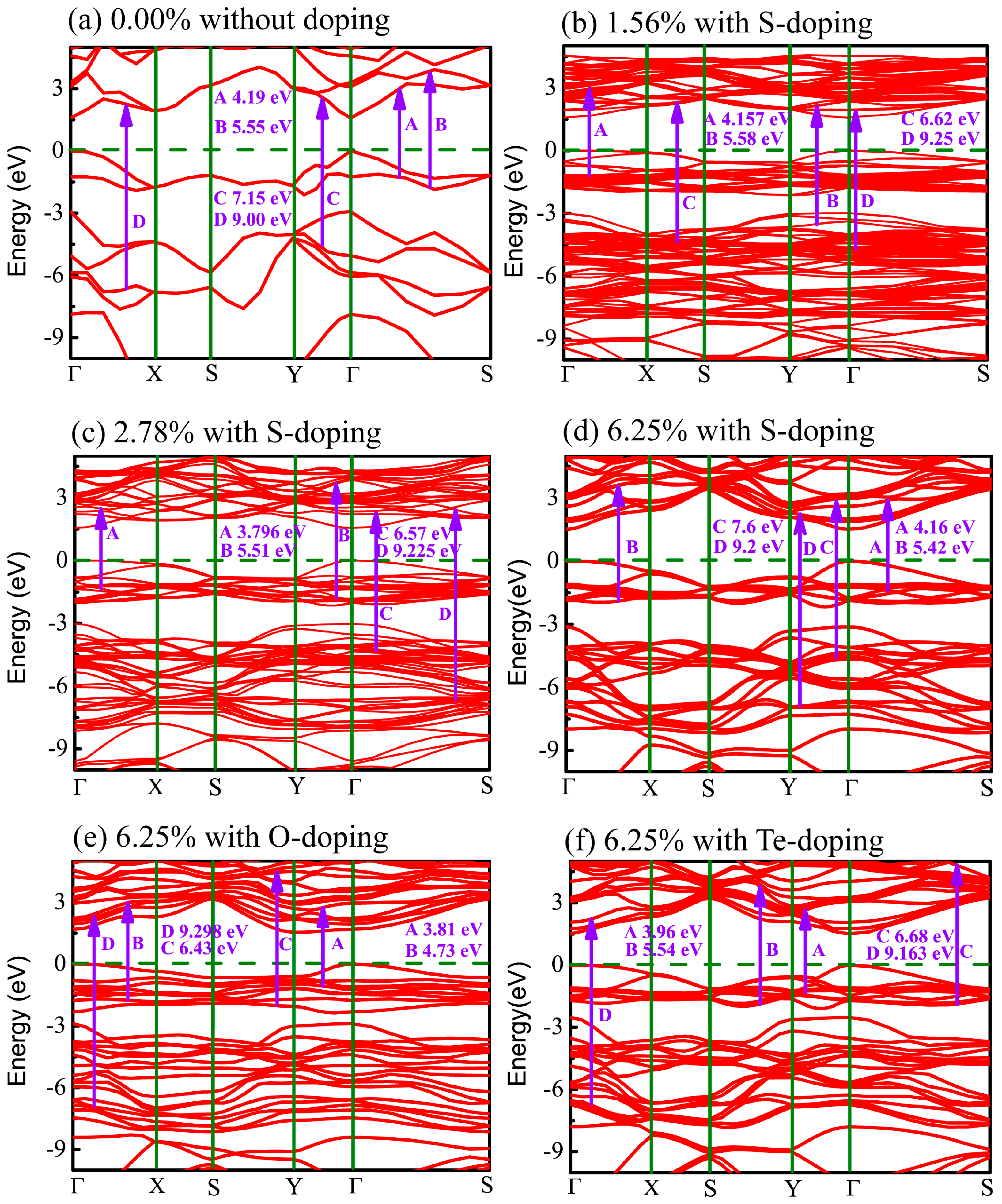
| Doped Atoms X | Concentration (%) | Band Gap (eV) | CBM | VBM |
|---|---|---|---|---|
| - | 0.00 | 1.59 | Γ | Γ |
| S | 1.56 | 1.52 | Γ | Γ |
| S | 2.78 | 1.48 | Γ | Γ |
| S | 6.25 | 1.43 | Γ | Γ |
| O | 6.25 | 1.54 | Y | Γ |
| Te | 6.25 | 1.39 | Γ | Γ |
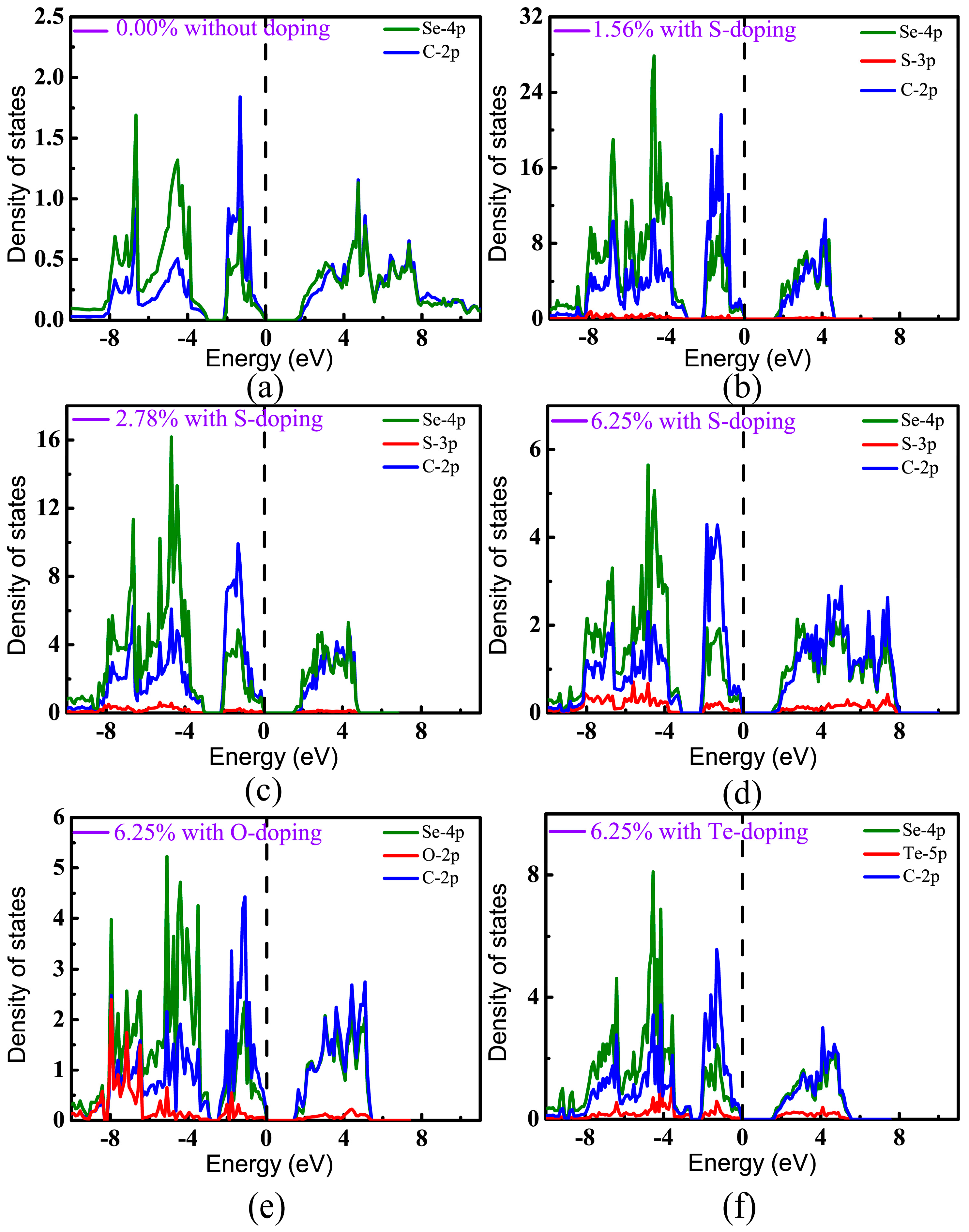
| Doped Atoms | Concentration | Bader Charge (e) | Charge Transfer (e) | ||||
|---|---|---|---|---|---|---|---|
| X | (%) | C | Se | X | From Se to C | From X to C | (eV) |
| - | 0.00 | 4.647 | 5.353 | - | 0.216 | - | - |
| S | 1.56 | 4.5832 | 5.3349 | 5.5876 | 0.2229 | 0.1375 | 0.01 |
| S | 2.78 | 4.5805 | 5.348 | 5.5919 | 0.2223 | 0.136 | 0.01 |
| S | 6.25 | 4.561 | 5.3550 | 5.621 | 0.2174 | 0.1263 | 0.01 |
| O | 6.25 | 4.115 | 5.3933 | 6.7682 | 0.1856 | −0.2561 | 0.87 |
| Te | 6.25 | 4.7933 | 5.3471 | 4.8877 | 0.2113 | 0.3708 | –0.47 |
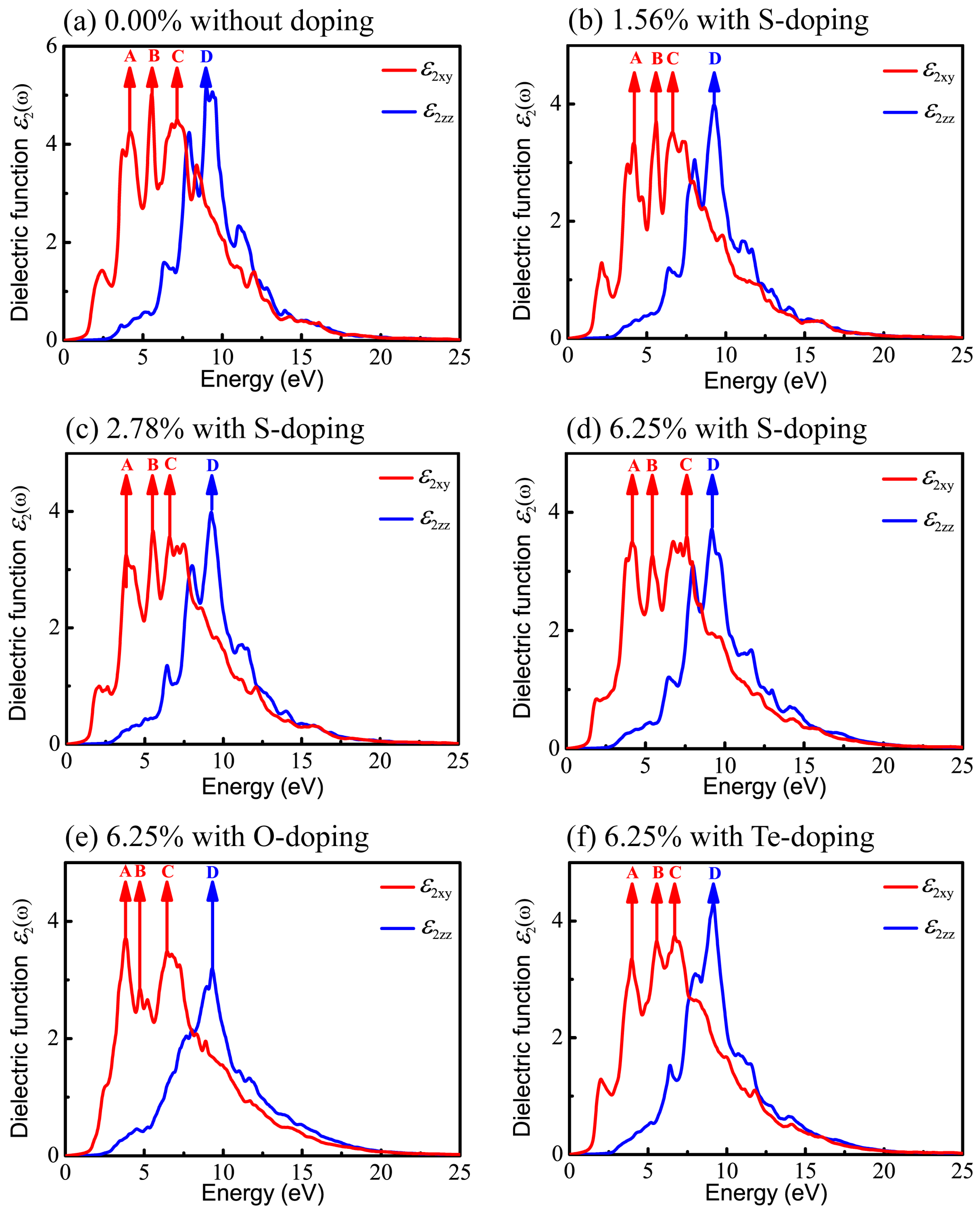
| Doped Atoms X | Concentration (%) | Peak Positions (eV) | |
|---|---|---|---|
| - | 0.00 | A = 4.19 | |
| - | - | B = 5.55 | |
| - | - | - | C = 7.15 |
| - | - | - | D = 9.00 |
| S | 1.56 | A = 4.157 | |
| - | - | B = 5.58 | |
| - | - | - | C = 6.62 |
| - | - | - | D = 9.25 |
| S | 2.78 | A = 3.796 | |
| - | - | B = 5.51 | |
| - | - | - | C = 6.57 |
| - | - | - | D = 9.225 |
| S | 6.25 | A = 4.16 | |
| - | - | B = 5.42 | |
| - | - | - | C = 7.60 |
| - | - | - | D = 9.20 |
| O | 6.25 | A = 3.81 | |
| - | - | B = 4.73 | |
| - | - | - | C = 6.43 |
| - | - | - | D = 9.298 |
| Te | 6.25 | A = 3.96 | |
| - | - | B = 5.54 | |
| - | - | - | C = 6.68 |
| - | - | - | D = 9.163 |
© 2018 by the authors. Licensee MDPI, Basel, Switzerland. This article is an open access article distributed under the terms and conditions of the Creative Commons Attribution (CC BY) license (http://creativecommons.org/licenses/by/4.0/).
Share and Cite
Zhang, Q.; Xin, T.; Lu, X.; Wang, Y. Optoelectronic Properties of X-Doped (X = O, S, Te) Photovoltaic CSe with Puckered Structure. Materials 2018, 11, 431. https://doi.org/10.3390/ma11030431
Zhang Q, Xin T, Lu X, Wang Y. Optoelectronic Properties of X-Doped (X = O, S, Te) Photovoltaic CSe with Puckered Structure. Materials. 2018; 11(3):431. https://doi.org/10.3390/ma11030431
Chicago/Turabian StyleZhang, Qiang, Tianyuan Xin, Xiaoke Lu, and Yuexia Wang. 2018. "Optoelectronic Properties of X-Doped (X = O, S, Te) Photovoltaic CSe with Puckered Structure" Materials 11, no. 3: 431. https://doi.org/10.3390/ma11030431
APA StyleZhang, Q., Xin, T., Lu, X., & Wang, Y. (2018). Optoelectronic Properties of X-Doped (X = O, S, Te) Photovoltaic CSe with Puckered Structure. Materials, 11(3), 431. https://doi.org/10.3390/ma11030431