Surface Sensitive Techniques for Advanced Characterization of Luminescent Materials


Abstract
:1. Introduction
2. Experimental Setup
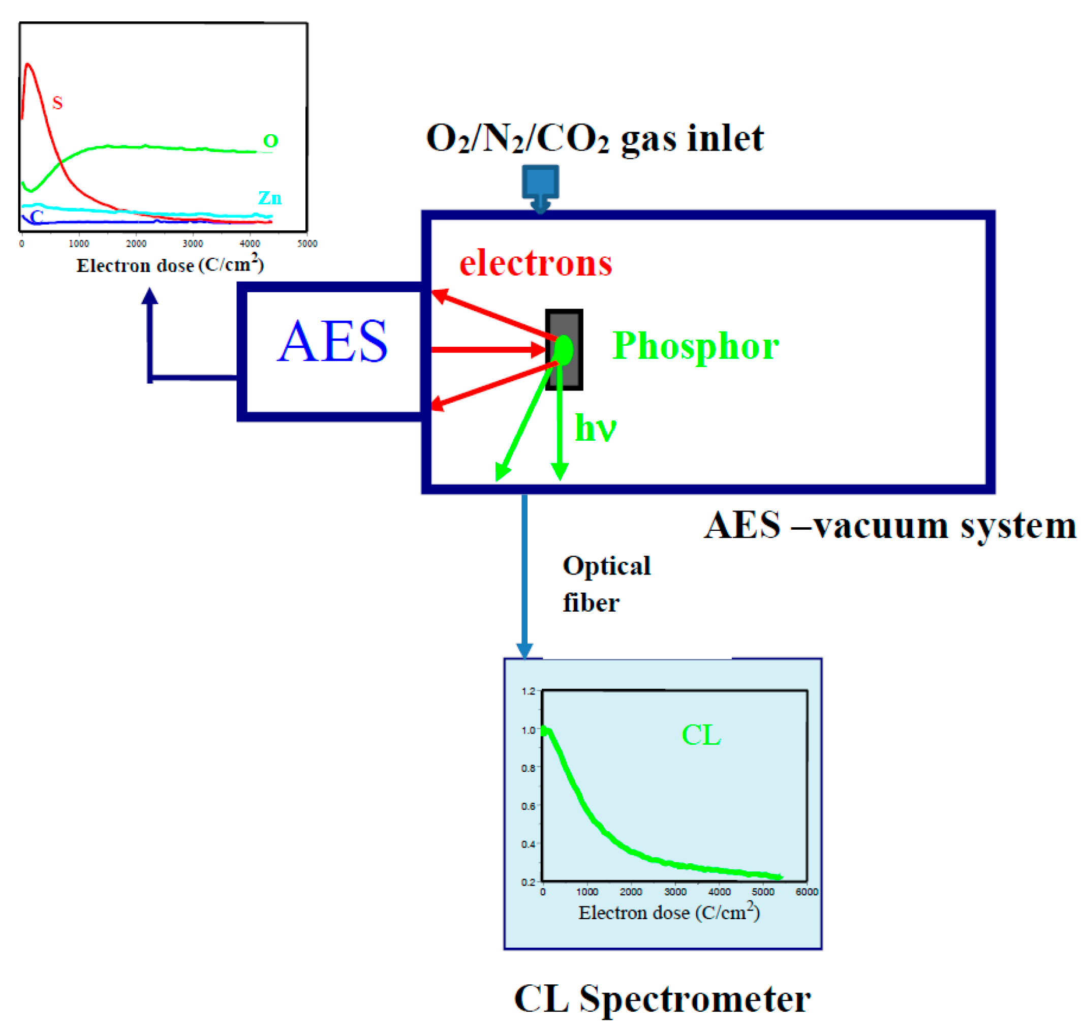
2.1. CL and AES
2.2. XPS
2.3. TOF-SIMS
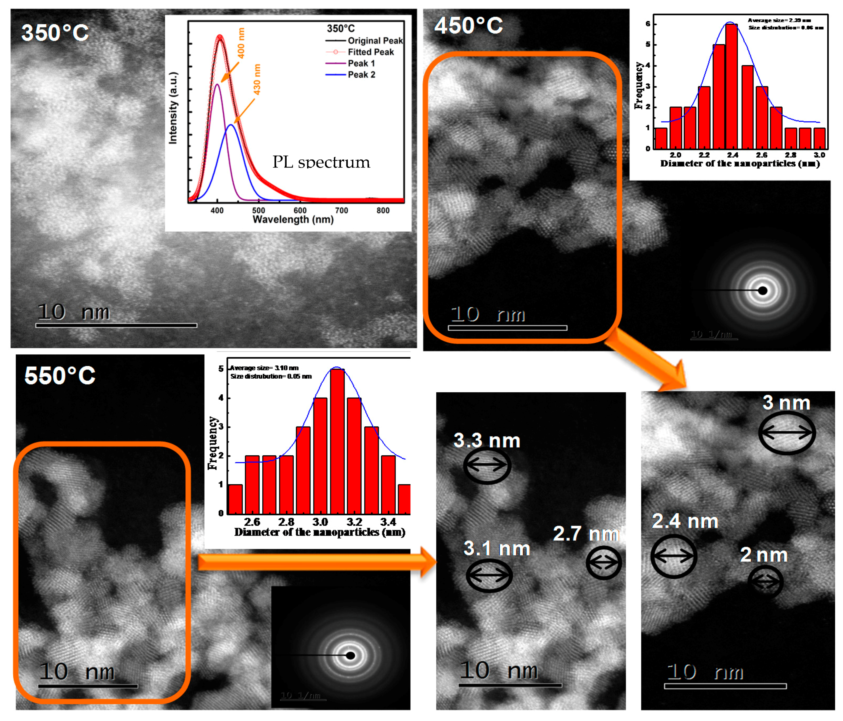
2.4. HRTEM
3. Results and Discussion
3.1. Electron Degradation—AES and XPS
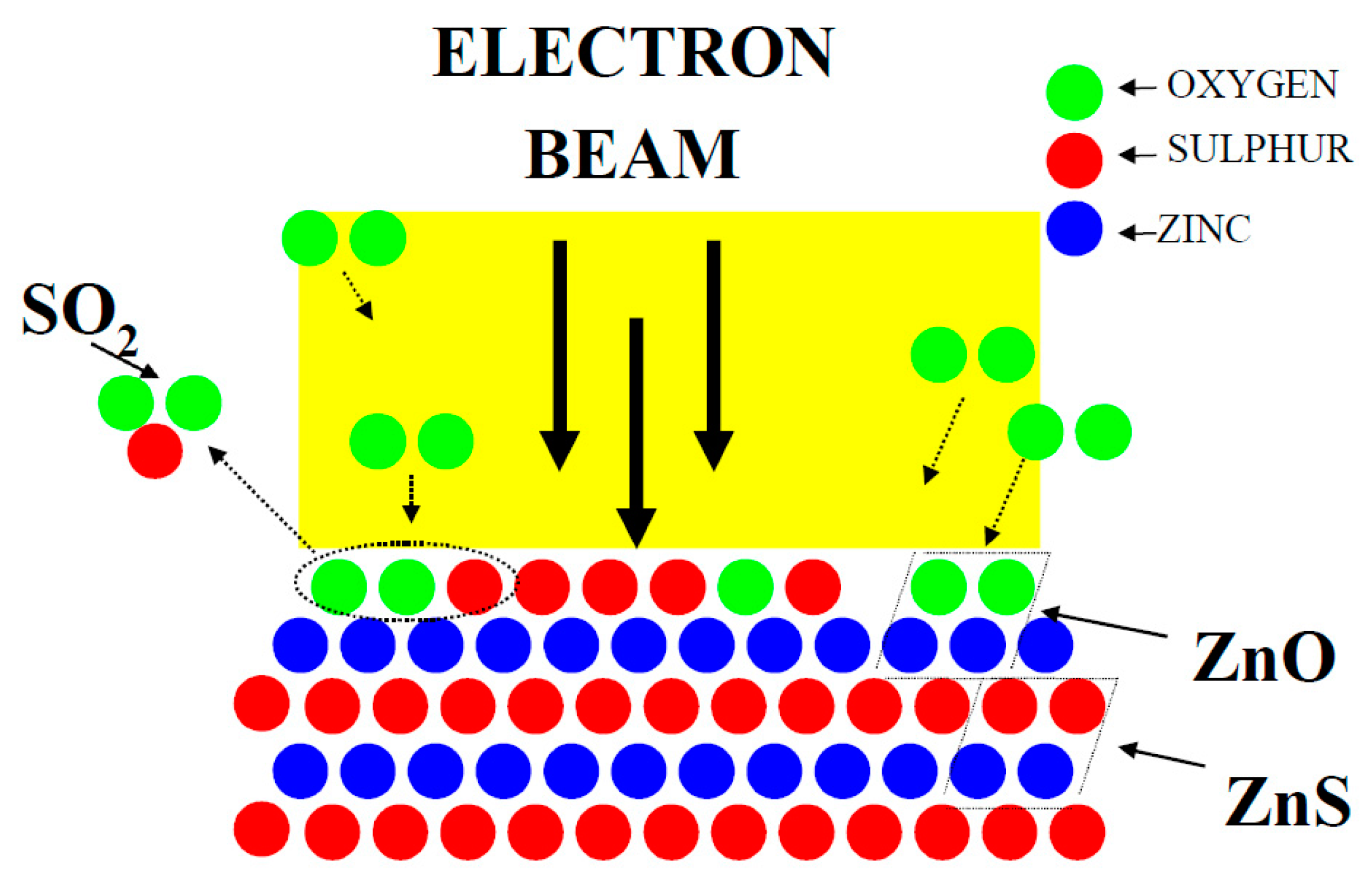
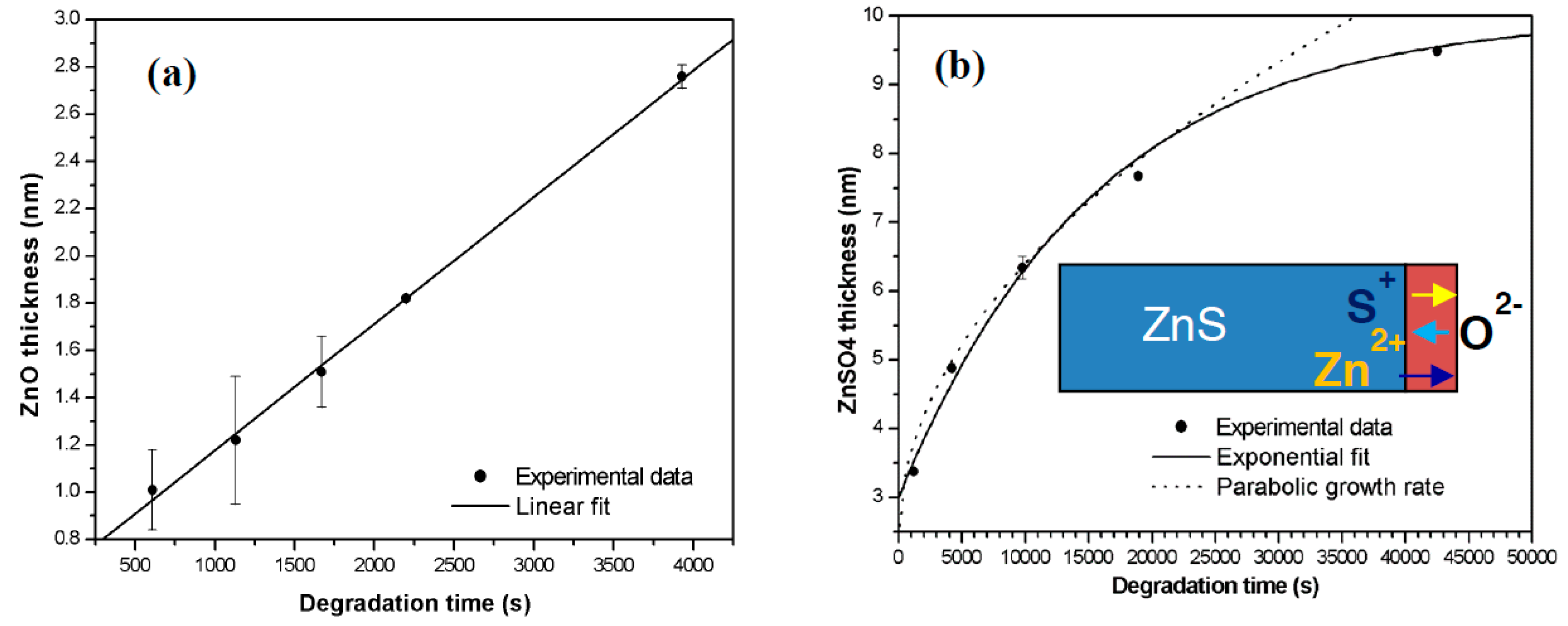
3.1.1. ZnS
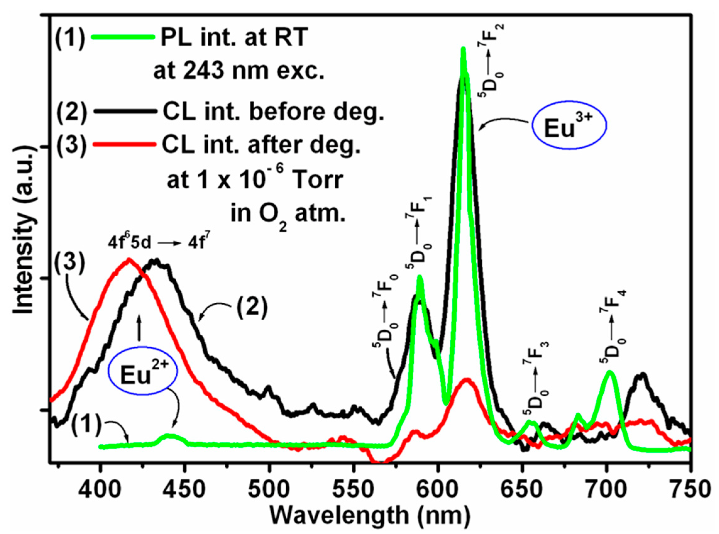
3.1.2. Sr5(PO4)3F:Eu
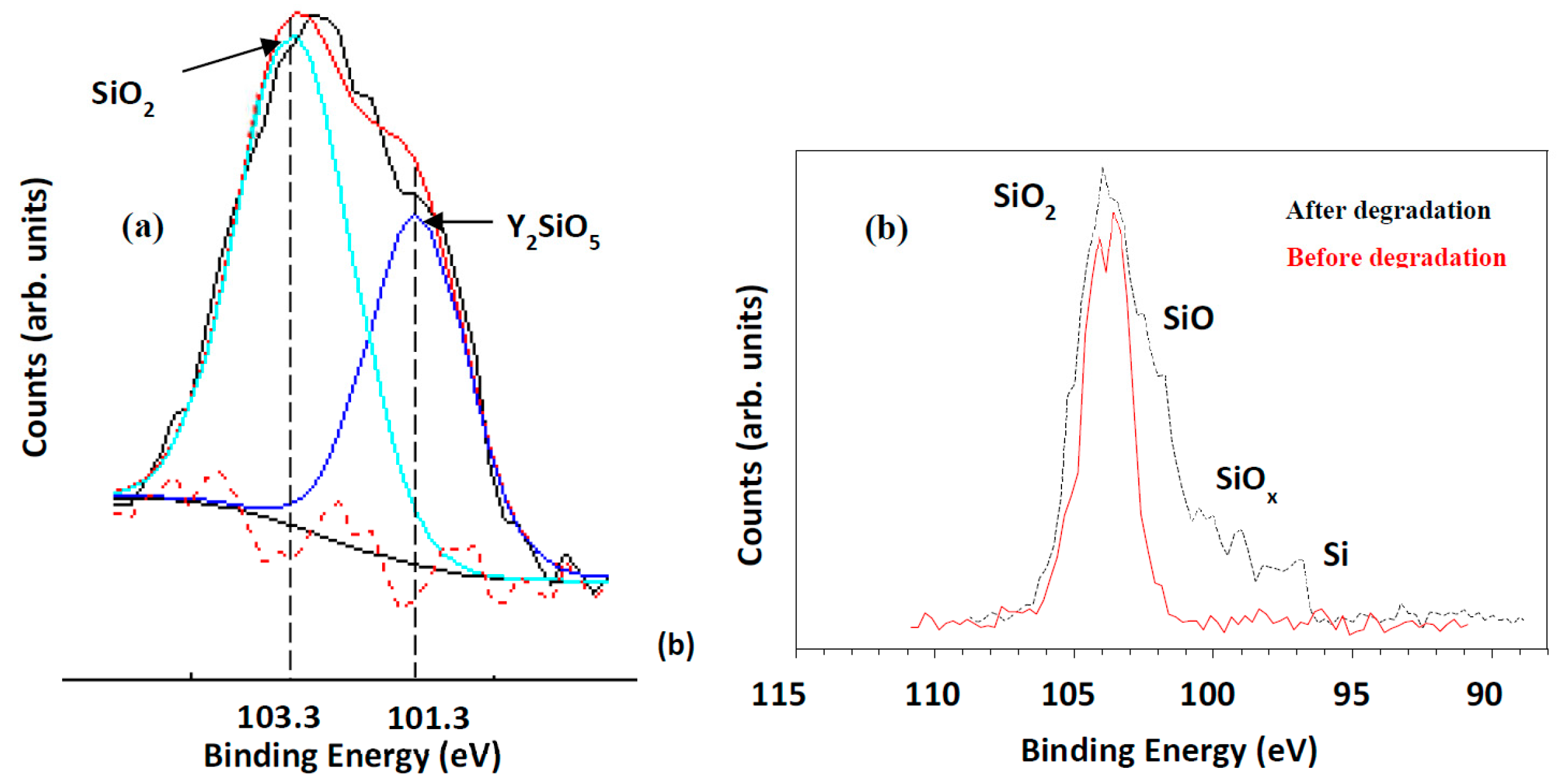
3.1.3. Y2SiO5:Ce3+
3.1.4. SiO2-PbS
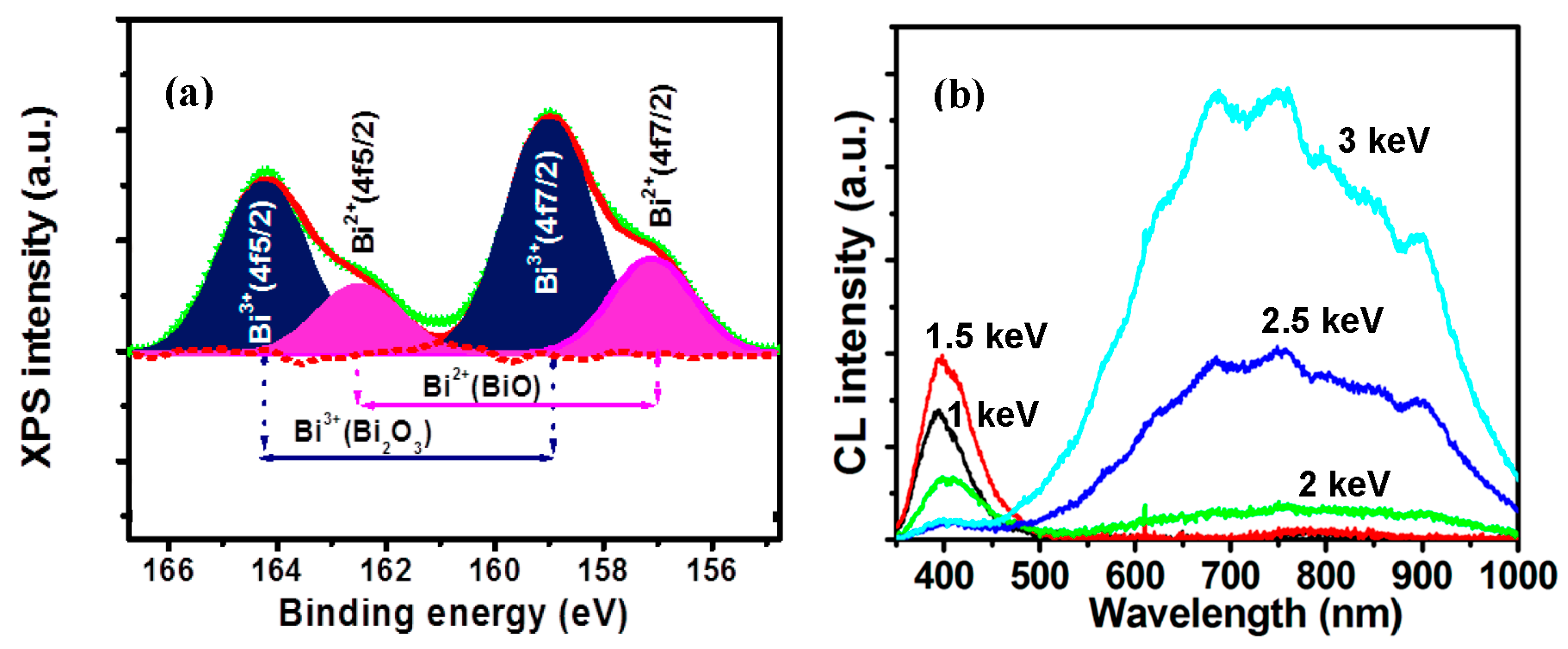
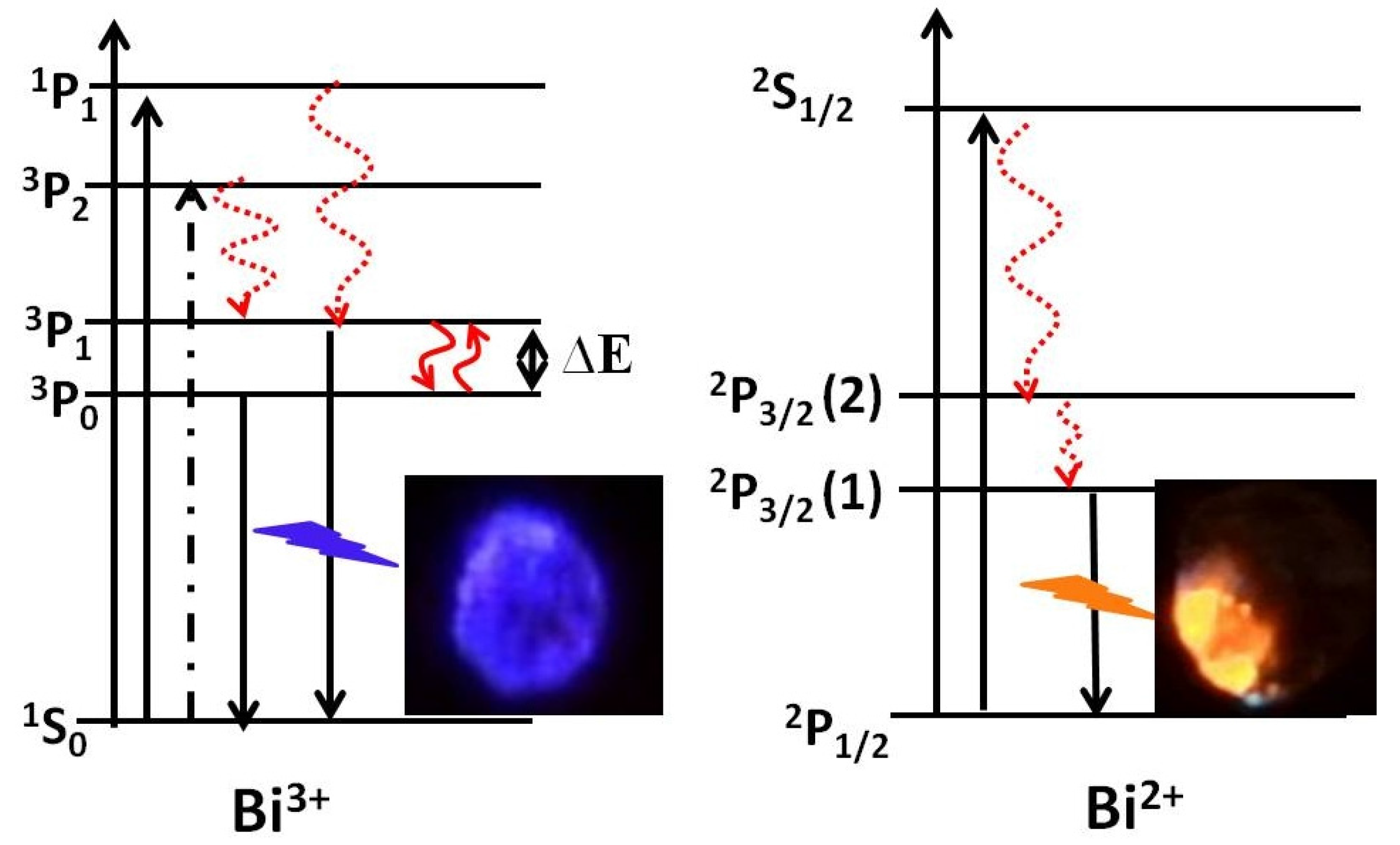
3.1.5. CaO:Bi
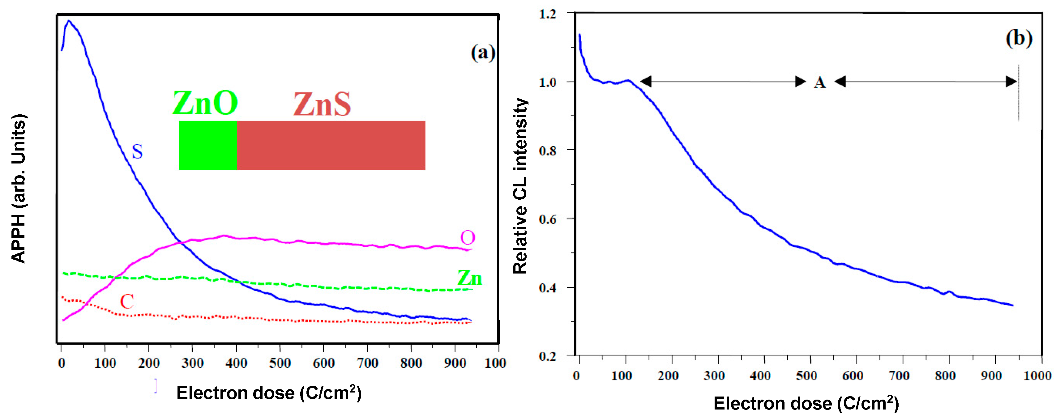
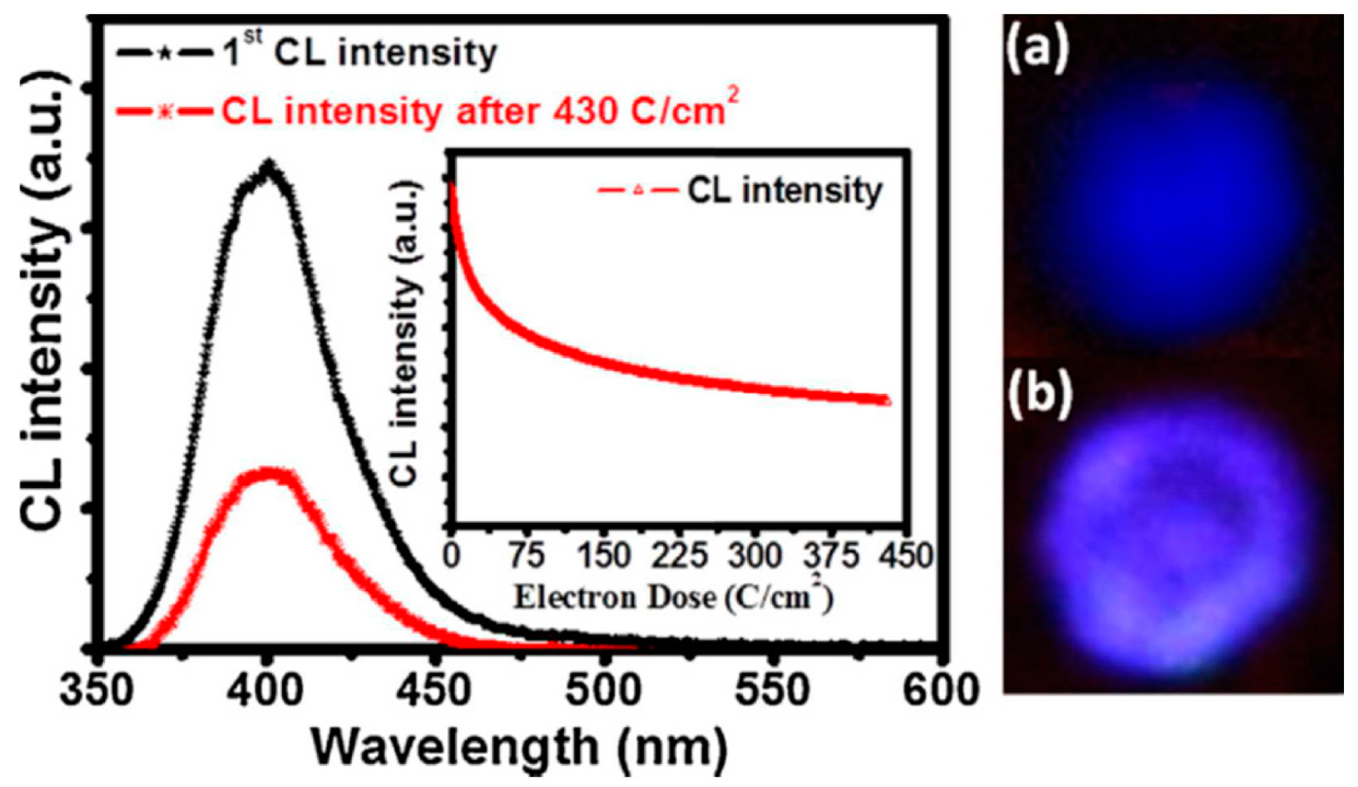
3.1.6. ZnO
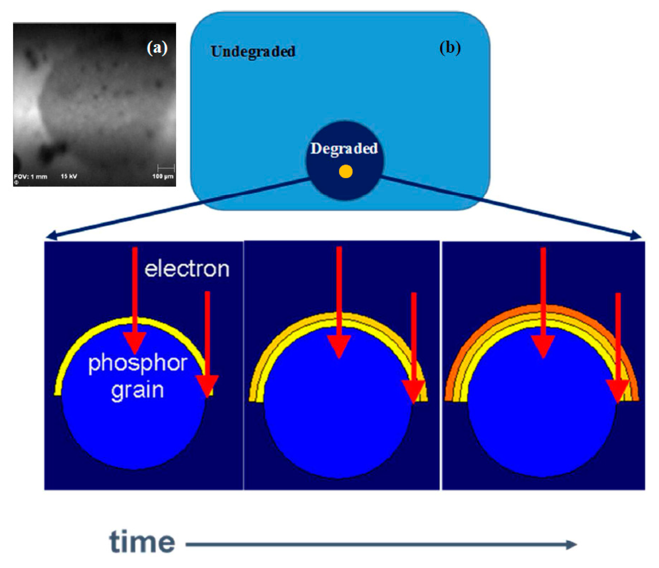
3.1.7. ESSCR Mechanism
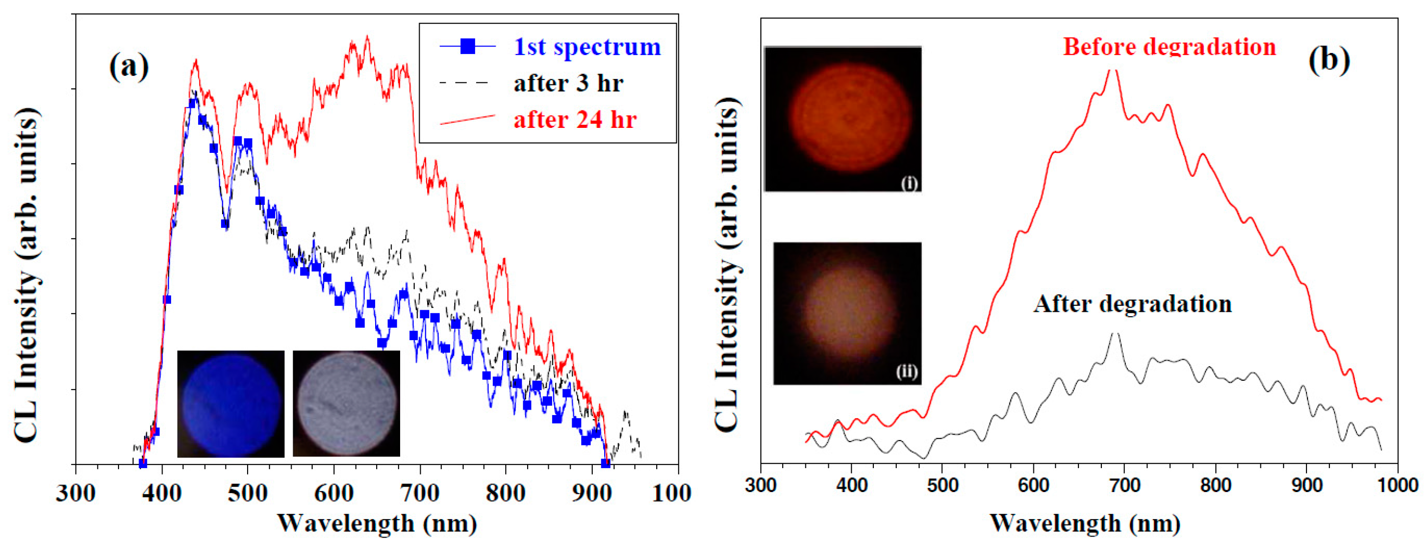
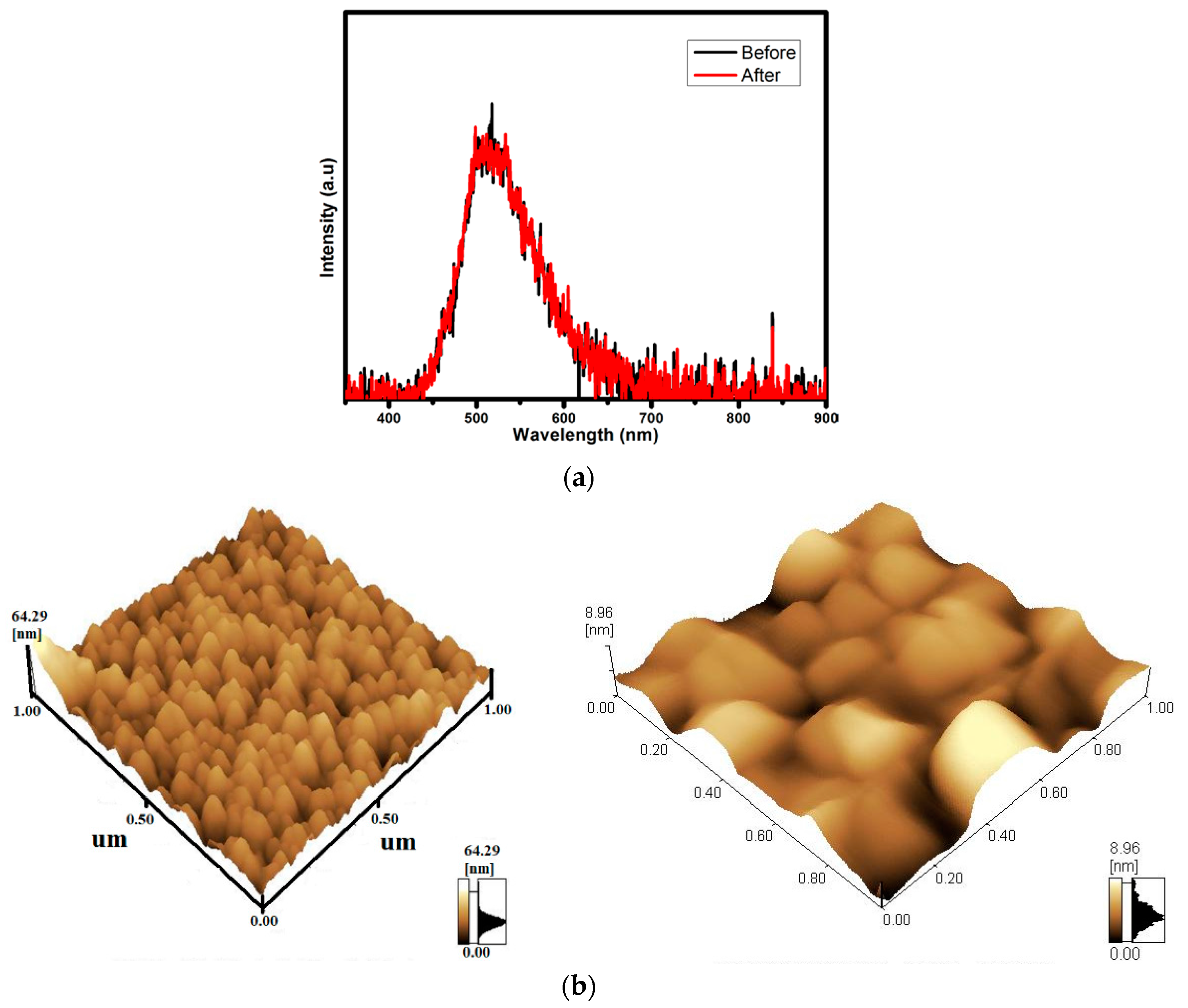
3.2. Defect Emission—XPS and HRTEM
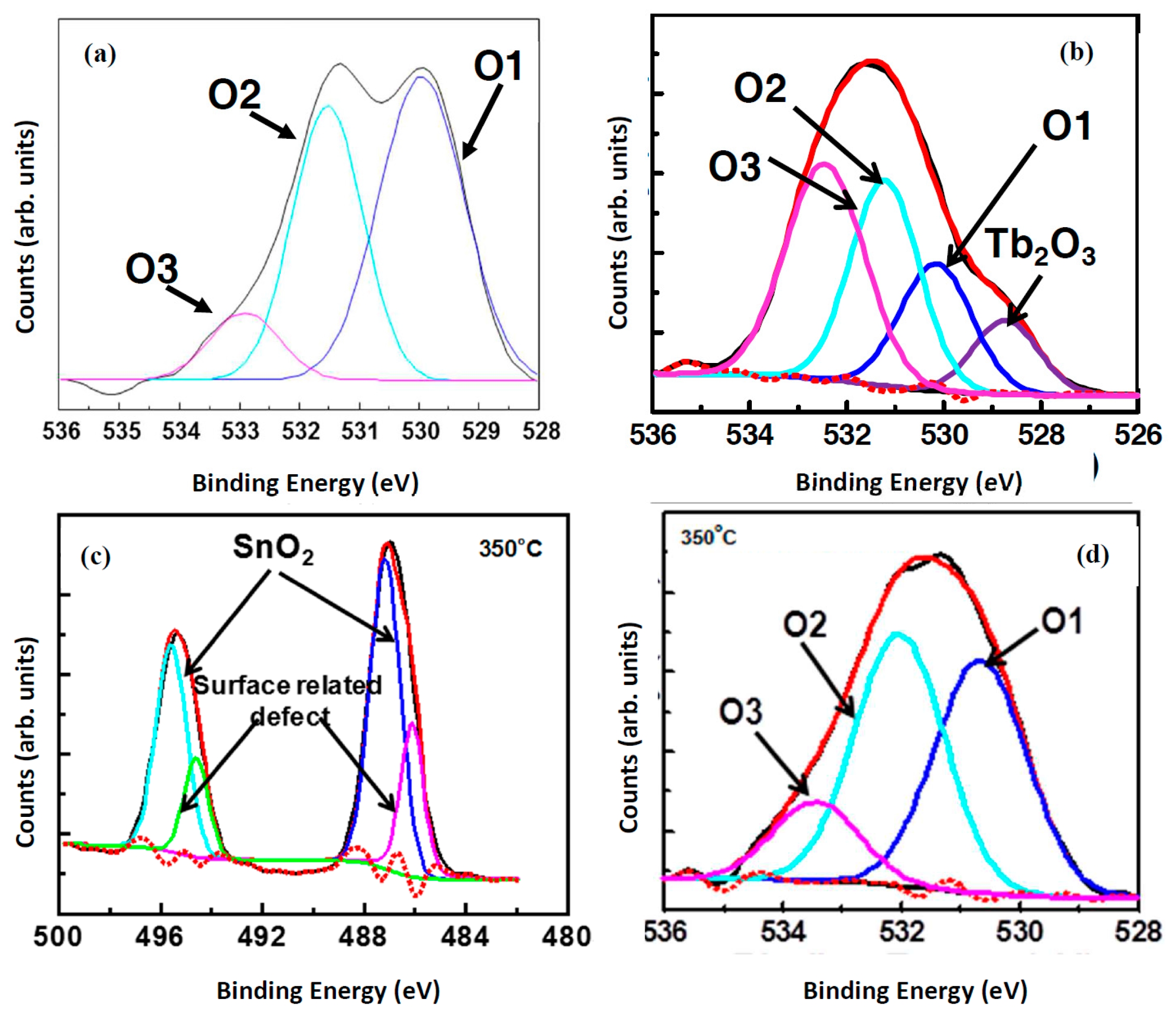
3.3. Oxidation/Valence State—XPS
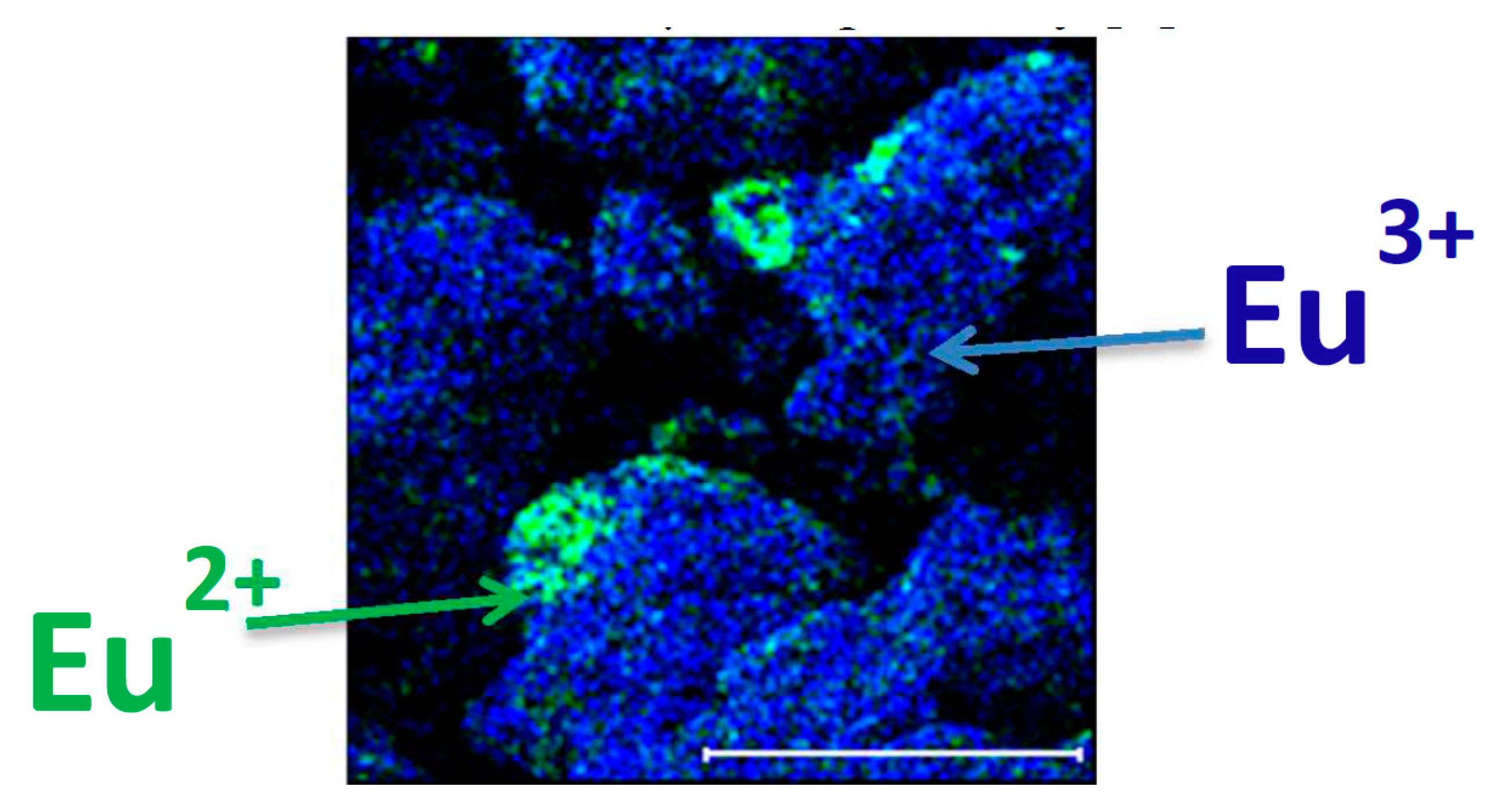
3.4. Oxidation/Valence State—TOF-SIMS
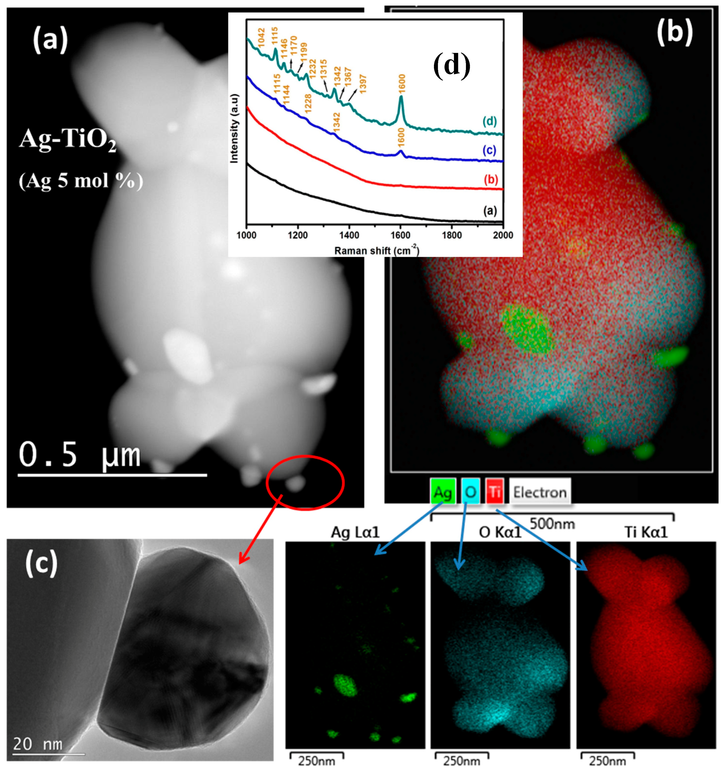
3.5. Surface Enhanced Raman Scattering
3.6. General
4. Conclusions
Acknowledgments
Author Contributions
Conflicts of Interest
References
- Swart, H.C.; Terblans, J.J.; Ntwaeaborwa, O.M.; Coetsee, E.; Mothudi, B.M.; Dhlamini, M.S. Photon emission mechanisms of different phosphors. Nucl. Instrum. Methods B 2009, 267, 2630–2633. [Google Scholar] [CrossRef]
- Shionoya, S.; Yen, W.M.; Yamamoto, H. Phosphor Handbook; CRC Press: Boca Raton, FL, USA, 1999. [Google Scholar]
- Tannas, L.E., Jr. Flat-Panel Displays and CRT’s; VanNostrand-Reinhold: New York, NY, USA, 1985. [Google Scholar]
- Kumar, V.; Swart, H.C.; Ntwaeaborwa, O.M.; Kroon, R.E.; Terblans, J.J.; Shaat, S.K.K.; Yousif, A.; Duvenhage, M.M. Origin of the red emission in zinc oxide nanophosphors. Mater. Lett. 2013, 110, 57–60. [Google Scholar] [CrossRef]
- Nagpure, I.M.; Pitale, S.S.; Coetzee, E.; Ntwaeaborwa, O.M.; Terblans, J.J.; Swart, H.C. Lattice site dependent cathodoluminescence behaviour and surface chemical changes in Sr5(PO4)3F host. Phys. B Phys. Condens. Matter 2012, 407, 1505–1508. [Google Scholar] [CrossRef]
- Mothudi, B.M.; Ntwaeaborwa, O.M.; Botha, J.R.; Swart, H.C. Photoluminescence and phosphorescence properties of MAl2O4:Eu2+,Dy3+ (M = Ca, Ba, Sr) phosphors prepared at an initiating combustion temperature of 500 °C. Phys. B Phys. Condens. Matter 2009, 404, 4440–4444. [Google Scholar] [CrossRef]
- Nagpure, I.M.; Pitale, S.S.; Coetsee, E.; Ntwaeaborwa, O.M.; Terblans, J.J.; Swart, H.C. Cathodoluminescence properties and surface characterization of Sr3(PO4)2:Tb phosphor. Appl. Surf. Sci. 2011, 257, 10147–10155. [Google Scholar] [CrossRef]
- Swart, H.C.; Terblans, J.J.; Ntwaeaborwa, O.M.; Kroon, R.E.; Coetsee, E.; Nagpure, I.M.; Kumar, V.; Kumar, V.; Kumar, V. Applications of AES, XPS and TOF SIMS to phosphor materials. Surf. Interface Anal. 2014, 46, 1105–1109. [Google Scholar] [CrossRef]
- Reisfeld, R.; Pantra, A.; Panczer, G.; Gaft, M. Spectroscopic properties of cerium in sol–gel glasses. Opt. Mater. 1999, 13, 81–88. [Google Scholar] [CrossRef]
- Meltzer, R.S.; Feofilov, A.P. Spectral hole burning in the 4f–5d transition of Ce3+ in LuPO4 and YPO4. J. Lumin. 2003, 102–103, 151–155. [Google Scholar] [CrossRef]
- Ganjali, M.R.; Zare-Dorabei, R.; Norouzi, P. Design and construction of a novel optical sensor for determination of trace amounts of dysprosium ion. Sens. Actuators B Chem. 2009, 143, 233–238. [Google Scholar] [CrossRef]
- Akinlua, A.; Torto, N.; Ajayi, T.R. Determination of rare earth elements in Niger Delta crude oils by inductively coupled plasma-mass spectrometry. Fuel 2008, 87, 1469–1477. [Google Scholar] [CrossRef]
- Zhang, N.; Huang, C.; Hu, B. ICP-AES determination of trace rare earth elements in environmental and food samples by on-line separation and preconcentration with acetylacetone-modified silica gel using microcolumn. Anal. Sci. 2007, 23, 997–1002. [Google Scholar] [CrossRef] [PubMed]
- Marsh, S.F. Separation of lanthanide fission products from nuclear fuels by extraction chromatography and cation exchange for isotope dilution mass spectrometric analysis. Anal. Chem. 1967, 39, 641–645. [Google Scholar] [CrossRef]
- Sun, S.; Wu, X.; Yang, J.; Li, L.; Wang, Y. Determination of dysprosium by resonance light scattering technique in the presence of BPMPHD. Spectrochim. Acta Part A 2004, 60, 261–264. [Google Scholar] [CrossRef]
- Li, J.; Liu, S.; Mao, X.; Gao, P.; Yan, Z. Trace determination of rare earths by adsorption voltammetry at a carbon paste electrode. J. Electroanal. Chem. 2004, 561, 137–142. [Google Scholar] [CrossRef]
- Sun, Y. Detailed study on simultaneous separation of rare earth elements by capillary electrophoresis. J. Chromatogr. A 2004, 1048, 245–251. [Google Scholar] [CrossRef]
- Orescanin, V.; Mikelic, L.; Roje, V.; Lulic, S. Determination of lanthanides by source excited energy dispersive X-ray fluorescence (EDXRF) method after preconcentration with ammonium pyrrolidine dithiocarbamate (APDC). Anal. Chim. Acta 2006, 570, 277–282. [Google Scholar] [CrossRef] [PubMed]
- Peter, B.S.; Panigrahi, K.S.; Viswanathan, C.K. Fluorescence enhancement of dysprosium, europium and terbium using sodium benzoate-trioctylphosphine oxide-Triton X-100. Anal. Chim. Acta 1992, 260, 135–141. [Google Scholar] [CrossRef]
- Sano, K.; Terada, H.; Hidaka, Y.; Nishio, H.; Amakawa, Y. Ion-Microprobe Analysis of Rare Earth Elements in Oceanic Basalt Glass. Anal. Sci. 1999, 15, 743–748. [Google Scholar] [CrossRef]
- Prasad, K.; Kala, R.; Rao, T.P.; Naidu, G.R.K. Ion imprinted polymer based ion-selective electrode for the trace determination of dysprosium(III) ions. Anal. Chim. Acta 2006, 566, 69–74. [Google Scholar] [CrossRef]
- Holloway, P.H.; Ntwaeaborwa, O.M.; Swart, H.C. Electron-Stimulated Surface Chemical Reactions on Phosphors. J. Vac. Sci. Technol. A 2013, 31, 1–12. [Google Scholar] [CrossRef]
- Abrams, B.L.; Holloway, P.H. Role of the surface in luminescent processes. Chem. Rev. 2004, 104, 5783–5801. [Google Scholar] [CrossRef] [PubMed]
- Knotek, M.L.; Feibelman, P.J. Stability of ionically bonded surfaces in ionizing environments. Surf. Sci. 1979, 90, 78–90. [Google Scholar] [CrossRef]
- Redhead, P.A.; Hobson, J.P.; Kornelsen, E.V. The Physical Basis of Ultrahigh Vacuum; Plenum Press: New York, NY, USA, 1952. [Google Scholar]
- Duvenhage, M.M.; Ntwaeaborwa, O.M.; Swart, H.C.; Visser, H.G. Synthesis, crystal structure, luminescent properties and photo degradation of mer-tris(8-Hydroxy-quinolinato-N,O)-indium(III) hydrate 0.5 methanol solvate. Opt. Mater. 2013, 35, 2366–2371. [Google Scholar] [CrossRef]
- Koao, L.F.; Dejene, F.B.; Swart, H.C.; Botha, J.R. The effect of Ce3+ on structure, morphology and optical properties of flower-like ZnO synthesized using the chemical bath method. J. Lumin. 2013, 143, 463–468. [Google Scholar] [CrossRef]
- Dutta, S.; Som, S.; Kunti, A.K.; Kumar, V.; Sharma, S.K.; Swart, H.C.; Visser, H.G. Structural and luminescence responses of CaMoO4 nano phosphors synthesized by hydrothermal route to swift heavy ion irradiation: Elemental and spectral stability. Acta Mater. 2017, 124, 109–119. [Google Scholar] [CrossRef]
- Yousif, A.; Swart, H.C. Colour tuneable emission from (Y1.995−xGax)2O3:Bi3+ phosphor prepared by a sol-gel combustion method. Mater. Lett. 2017, 186, 345–348. [Google Scholar] [CrossRef]
- Pitale, S.S.; Nagpure, I.M.; Kumar, V.; Ntwaeaborwa, O.M.; Terblans, J.J.; Swart, H.C. Investigations on the low voltage cathodoluminescence stability and surface chemical behaviour using Auger and X-ray photoelectron spectroscopy on LiSrBO3:Sm3+ phosphor. Mater. Res. Bull. 2011, 46, 987–994. [Google Scholar] [CrossRef]
- Noto, L.L.; Pitale, S.S.; Gusowki, M.A.; Terblans, J.J.; Ntwaeaborwa, O.M.; Swart, H.C. Afterglow enhancement with In3+codoping in CaTiO3:Pr3+ red phosphor. Powder Technol. 2013, 237, 141–146. [Google Scholar] [CrossRef]
- Moulder, F.; Stickle, W.F.; Sobol, P.E.; Bomben, K.D. Handbook of X-ray Photoelectron Spectroscopy; ULVAC-PHI, Inc.: Chigasaki, Japan, 1995. [Google Scholar]
- Oosthuizen, L.; Swart, H.C.; Viljoen, P.E.; Holloway, P.H.; Berning, G.L.P. Phosphor degradation under electron excitation. Appl. Surf. Sci. 1997, 120, 9–14. [Google Scholar] [CrossRef]
- Itoh, S.; Kimizuka, T.; Tonegawa, T. Degradation Mechanism for Low Voltage Cathodoluminescence of Sulfide Phosphors. J. Electrochem. Soc. 1989, 136, 1819. [Google Scholar] [CrossRef]
- Chen, S.H.; Greeff, A.P.; Swart, H.C. Degradation of ZnS:Cu,Al,Au phosphor powder in different gas mixtures. J. Lumin. 2004, 109, 93–102. [Google Scholar] [CrossRef]
- Swart, H.C.; Sebastian, J.S.; Trottier, T.A.; Jones, S.L.; Holloway, P.H. Degradation of Zinc Sulfide Phosphors under electron bombardment. J. Vac. Sci. Technol. A 1996, 14, 1697–1703. [Google Scholar] [CrossRef]
- Holloway, P.H.; Sebastian, J.S.; Trottier, T.A.; Swart, H.C.; Peterson, R.O. Production and control of vacuum in Field Emission Flat Panel Displays. Solid State Technol. 1995, 38, 47–54. [Google Scholar]
- Pitale, S.S.; Kumar, V.; Nagpure, I.M.; Coetsee, E.; Ntwaeaborwa, O.M.; Swart, H.C. Cathodoluminescent properties and surface characterization of bluish-white nanocrystalline LiAl5O8:Tb phosphor. J. Appl. Phys. 2011, 109, 013105. [Google Scholar] [CrossRef]
- Richardson, F.S. Terbium(III) and europium(III) ions as luminescent probes and stains for biomolecular systems. Chem. Rev. 1982, 82, 541. [Google Scholar] [CrossRef]
- Nsimama, P.D.; Ntwaeaborwa, O.M.; Swart, H.C. Auger electron/X-ray photoelectron and Cathodoluminescent Spectroscopic Studies of Pulsed Laser Ablated SrAl2O4:Eu2+,Dy3+ Thin Films. Appl. Surf. Sci. 2010, 257, 512. [Google Scholar] [CrossRef]
- Shah, K.V.; Goswami, M.; Manikandan, S.; Shrikhande, V.K.; Kothiyal, G.P. Surface degradation behaviour of sodium borophosphate glass in aqueous media: Some studies. Bull. Mater. Sci. 2009, 32, 329. [Google Scholar] [CrossRef]
- Coetsee, E.; Terblans, J.J.; Swart, H.C. Degradation of Y2SiO5:Ce phosphor powders. J. Lumin. 2007, 126, 37–42. [Google Scholar] [CrossRef]
- Zhang, Q.Y.; Pita, K.; Buddhudu, S.; Kam, C.H. Luminescent properties of rare-earth ion doped yttrium silicate thin film phosphors for a full-colour display. J. Phys. D Appl. Phys. 2002, 35, 3085. [Google Scholar] [CrossRef]
- Bosze, E.J.; Hirata, G.A.; McKittrick, J. An Investigation of the Chromaticity of Blue Emitting Yttrium Silicate. Proc. Mater. Res. Soc. 1999, 558, 15. [Google Scholar] [CrossRef]
- Liu, X.; Phang, J.C.H.; Chan, D.S.H.; Chim, W.K. The properties of 2.7 eV cathodoluminescence from SiO2 film on Si substrate. J. Phys. D Appl. Phys. 1999, 32, 1563. [Google Scholar] [CrossRef]
- Skuja, L.N.; Entzian, W. Cathodoluminescence of Intrinsic Defects in Glassy SiO2, Thermal SiO2 Films, and α-Quartz. Phys. Status Solidi A 1986, 96, 191. [Google Scholar] [CrossRef]
- Dhlamini, M.S.; Terblans, J.J.; Ntwaeaborwa, O.M.; Swart, H.C. Synthesis and degradation of the PbS nanoparticle phosphors embedded in SiO2, (SiO2:PbS). Surf. Rev. Lett. 2007, 14, 697–701. [Google Scholar] [CrossRef]
- Yousif, A.; Jafer, R.M.; Som, S.; Swart, H.C. Ultra-broadband luminescent from Bi doped CaO matrix. RSC Adv. 2015, 5, 54115–54122. [Google Scholar] [CrossRef]
- Hasabeldaim, E.; Ntwaeaborwa, O.M.; Kroon, R.E.; Craciun, V.; Coetsee, E.; Swart, H.C. Surface characterization and cathodoluminescence degradation of ZnO thin films. Appl. Surf. Sci. 2016. [Google Scholar] [CrossRef]
- Swart, H.C.; Oosthuizen, L.; Holloway, P.H.; Berning, G.L.P. The degradation behaviour of ZnS phosphor powders under different experimental conditions. Surf. Interface Anal. 1998, 26, 337–342. [Google Scholar] [CrossRef]
- Swart, H.C.; Hillie, K.T.; Greeff, A.P. The effect of temperature on the degradation of ZnS FED phosphors. Surf. Interface Anal. 2001, 32, 110–113. [Google Scholar] [CrossRef]
- Kumar, V.; Som, S.; Kumar, V.; Kumar, V.; Ntwaeaborwa, O.M.; Coetsee, E.; Swart, H.C. Tunable and white emission from ZnO:Tb3+ nanophosphors for solid state lighting applications. Chem. Eng. J. 2014, 255, 541–552. [Google Scholar] [CrossRef]
- Ahmad, M.; Pan, C.; Luo, Z.; Zhu, J.A. A Single ZnO Nanofiber-Based Highly Sensitive Amperometric Glucose Biosensor. J. Phys. Chem. C 2010, 114, 9308–9313. [Google Scholar] [CrossRef]
- Pereira, A.S.; Peres, M.; Soares, M.J.; Alves, E.; Neves, A.; Monteiro, T.; Trindade, T. Synthesis, surface modification and optical properties of Tb3+-doped ZnO nanocrystals. Nanotechnology 2006, 17, 834. [Google Scholar] [CrossRef]
- Kumar, V.; Kumar, V.; Som, S.; Neethling, J.; Olivier, E.J.; Ntwaeaborwa, O.M.; Swart, H.C. Role of surface and deep-level defect on the emission of tin oxide quantum dots. Nanotechnology 2014, 25, 135701. [Google Scholar] [CrossRef] [PubMed]
- Vila, M.; Guerra, C.; Lorenz, K.; Piqueras, J.; Alves, E.; Nappinic, S.; Magnanoc, E. Structural and luminescence properties of Eu and Er implanted Bi2O3 nanowires for optoelectronic applications. J. Mater. Chem. C 2013, 1, 7920. [Google Scholar] [CrossRef]
- Cao, R.; Zhang, F.; Liao, C.; Qiu, J. Yellow-to-orange emission from Bi2+-doped RF2 (R = Ca and Sr) phosphors. Opt. Express 2013, 21, 15728. [Google Scholar] [CrossRef] [PubMed]
- Zhang, C.M.; Yang, J.; Lin, C.K.; Li, C.X.; Lin, J. Reduction of Eu3+ to Eu2+ in MAl2Si2O8 (M = Ca, Sr, Ba) in air condition. J. Solid State Chem. 2009, 182, 1673. [Google Scholar] [CrossRef]
- Swart, H.C.; Nagpure, I.M.; Ntwaeaborwa, O.M.; Fisher, G.L.; Terblans, J.J. Identification of Eu Oxidation States in a Doped Sr5(PO4)3F Phosphor by TOF-SIMS Imaging. Opt. Express 2012, 20, 17119–17125. [Google Scholar] [CrossRef]
- Ahmed, H.A.A.S.; Swart, H.C.; Kroon, R.E. Investigating the capability of ToF-SIMS to determine the oxidation state of Ce ions. Phys. B Condens. Matter 2017. [Google Scholar] [CrossRef]
- Prakash, J.; Kumar, P.; Harris, R.A.; Swart, C.; Neethling, J.H.; van Vuuren, A.J.; Swart, H.C. Synthesis, Characterization and Multifunctional Properties of Plasmonic Ag-TiO2. Nanotechnology 2016, 27, 355707. [Google Scholar] [CrossRef] [PubMed]
- Chen, S.F.; Li, J.P.; Qian, K.; Xu, W.P.; Lu, Y.; Huang, W.X.; Yu, S.H. Large scale photochemical synthesis of M@TiO2 nanocomposites (M = Ag, Pd, Au, Pt) and their optical properties, CO oxidation performance, and antibacterial effect. Nano Res. 2010, 3, 244–255. [Google Scholar] [CrossRef]


© 2017 by the author. Licensee MDPI, Basel, Switzerland. This article is an open access article distributed under the terms and conditions of the Creative Commons Attribution (CC BY) license (http://creativecommons.org/licenses/by/4.0/).
Share and Cite
Swart, H.C. Surface Sensitive Techniques for Advanced Characterization of Luminescent Materials. Materials 2017, 10, 906. https://doi.org/10.3390/ma10080906
Swart HC. Surface Sensitive Techniques for Advanced Characterization of Luminescent Materials. Materials. 2017; 10(8):906. https://doi.org/10.3390/ma10080906
Chicago/Turabian StyleSwart, Hendrik C. 2017. "Surface Sensitive Techniques for Advanced Characterization of Luminescent Materials" Materials 10, no. 8: 906. https://doi.org/10.3390/ma10080906
APA StyleSwart, H. C. (2017). Surface Sensitive Techniques for Advanced Characterization of Luminescent Materials. Materials, 10(8), 906. https://doi.org/10.3390/ma10080906