1. Introduction
Because of the rapid increase in the global population and energy consumption, electric vehicles (EVs) that use clean energy sources connected to dc-microgrids have been proposed as favorable and environmentally friendly alternatives to conventional vehicles [
1,
2,
3,
4,
5]. A dc-microgrid comprises a grid-connected converter (GCC), the different types of distributed energy generation systems, a battery storage system, EVs, and local emergency loads. The function of the GCC is to maintain a constant dc-bus voltage. To ensure the operational reliability of the dc-microgrid, a mass of battery storage devices is usually added to the system. EVs provide ancillary services to the dc-microgrid, which facilitates clean and efficient electric-powered transportation by enabling the EVs to power or be powered by the grid.
In hybrid electric vehicles (HEVs), fuel cell (FC) stacks can be used as clean energy sources. FCs are energy sources that directly convert chemical energy to electrical energy. FCs generate electric energy and, rather than storing it, continue to deliver the energy as long as the fuel supply is maintained. However, FCs have the drawbacks of slow dynamic response and high cost per output power [
2,
6,
7,
8,
9]. Thus, FCs alone are not used in HEVs to satisfy load demands, particularly during startup and transient events. Therefore, to solve these problems, FCs are generally used with the battery storage device. Furthermore, the combined use of FCs and the battery storage device reduces hydrogen consumption in the FCs [
3,
6,
7,
8,
9].
In general, FCs and batteries have different voltage levels. Therefore, to provide a specific voltage level for the load and control power flow between the input sources, a power converter is required for each of the input sources; this increases the price, mass, and losses. To overcome these drawbacks, multiport converters have been used in hybrid power systems [
10,
11,
12,
13,
14,
15,
16,
17,
18,
19,
20,
21]. These converters are of two main types: isolated and nonisolated. In isolated converters, high-frequency transformers are used to provide galvanic isolation. Several types of isolated converters, such as half-bridge, full-bridge, dual-active bridge, boost half-bridge, and combinational multiport isolated converters, have been investigated [
10,
11,
12,
13,
14,
15,
16,
17].
According to the literature, usage of nonisolated converters in EV applications is more useful. A multi-input buck converter was introduced in [
20]. The advantage of this converter is that it reduces the number of inductors and capacitors, leading to lower converter cost, volume, and weight. However, lack of an effective power flow control between the input sources is a disadvantage. A multiphase converter was introduced in [
21]. In this converter, each of the energy sources can deliver or absorb energy from the load and other sources. Using a separate inductor for each input source is a drawback of this converter. A triple input converter for hybridization of the battery, photovoltaic cells, and the FC was introduced in [
22]. Appropriately switching this converter enables the charging and discharging of the battery through other sources and load, respectively. A systematic approach for deriving nonisolated multi-input converter topologies through a combination of buck, boost, Ćuk, and SEPIC was presented in [
23]. A multi-input converter with only one inductor was proposed in [
24]; this converter distributes the load power between the input sources and enables power transfer between the sources. A nonisolated multi-input–multi-output (MIMO) converter comprising only one inductor was introduced in [
25]. However, this converter uses a high number of switches, which causes low efficiency. Moreover, the converter cannot transfer energy between the input sources. To overcome these drawbacks, a new nonisolated MIMO boost converter was proposed [
26]. This converter is used in hybridizing clean energy sources in EVs. The basic boost converter is modified and integrated; however, in practice, the voltage gain of the MIMO boost converter is limited owing to the losses associated with the inductor, filter capacitor, main power switch, and rectifier diode. Because of a very high duty ratio, the output rectifier conducts for an extremely short time during each switching cycle, thus resulting in major reverse-recovery problems and an increase in the rating of the rectification diode. The switch-off loss due to the rectifier diode affects the efficiency, resulting in the electromagnetic interference problem that is severe in this condition.
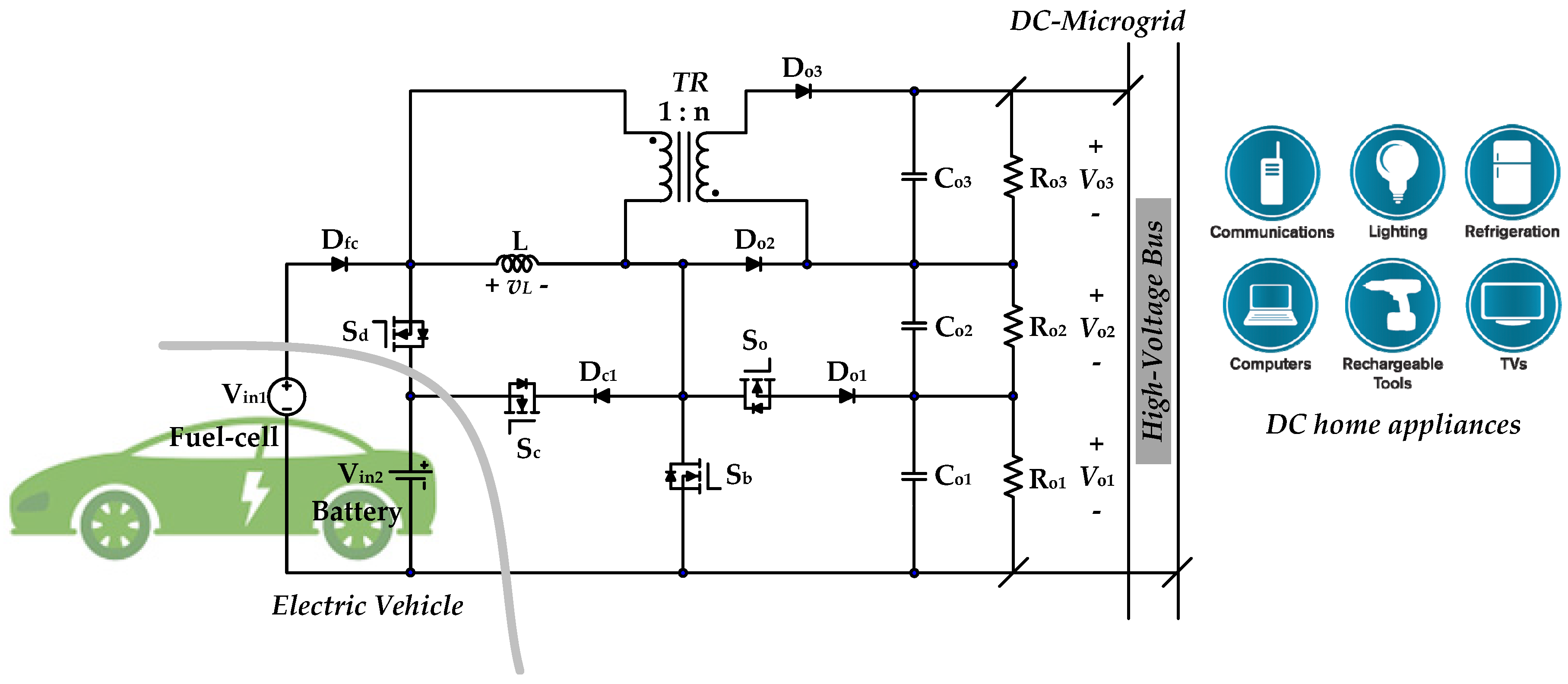
This paper proposes a high-gain three-port power converter with FC, battery sources and stacked output for an HEV connected to a dc-microgrid. In the proposed converter, the load power can be flexibly distributed between the input sources. Moreover, the charging or discharging of a battery storage device can be controlled effectively using the FC source. The proposed converter comprises only one boost inductor integrated with a flyback transformer; the boost and flyback circuit output terminals are stacked to increase the output voltage gain, making it suitable for interfacing with dc-microgrid. The stacked output structure of the proposed converter enables all the voltage stresses of power devices to be distributed and reduced. Therefore, the high performance and relatively lower drain-source voltage (i.e., VDS) aids in further reducing both switching and conduction losses. This paper presents the circuit configuration, operating principle, and steady-state analysis of the proposed converter. The validity of the proposed power converter and its performance were verified by simulation and experimental results under different operating conditions. The highest conversion efficiency achieved by the prototype was 96.6% in the battery discharging mode with two input sources of Vin1 = 36 V and Vin2 = 48 V.
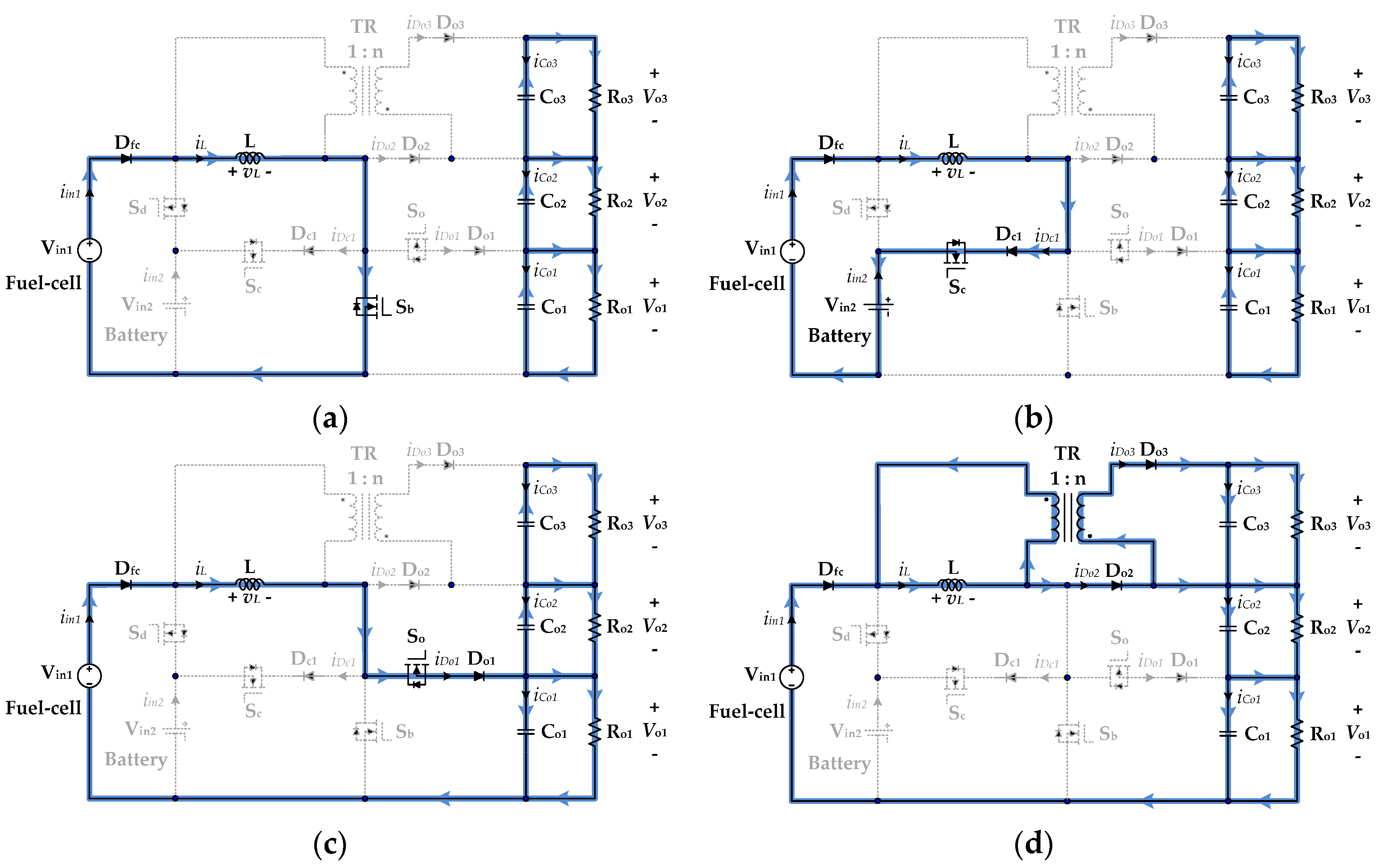
2. Topology and Operation Modes of the Proposed Power Converter
The proposed converter topology was derived on the basis of a nonisolated MIMO boost converter [
26]; the system structure of the proposed converter is shown in
Figure 1. The proposed power converter receives the HEV electrical power from the FC and battery sources and converts it to a suitable high voltage, which is applied to a dc-microgrid so that dc home appliances can use the electricity directly. In
Figure 1,
Ro1–Ro3 are the load resistances that represent the equivalent power feeding dc-microgrid. The four power switches
Sc,
Sd,
Sb, and
So in the converter structure are the main active switches that control the power flow and output voltages of the converter. In the proposed converter, source
Vin1 can deliver power to source
Vin2 but not
vice versa. In this study, the FC was used as a generating power source (
Vin1), and the battery was used as a storage device (
Vin2). On the basis of the utilization state of the battery, two power operating modes were defined and investigated for the proposed converter as follows.
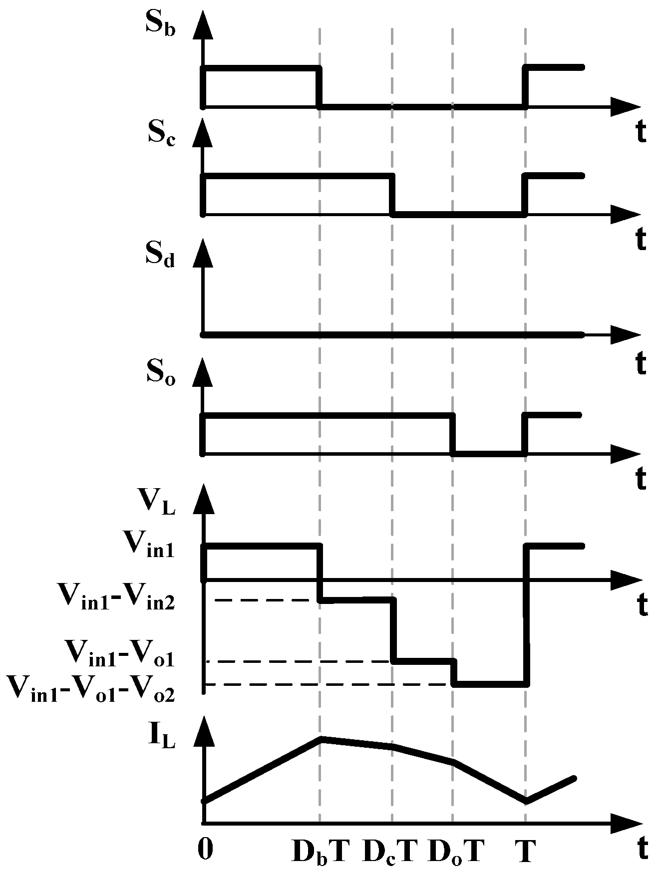
2.1. Battery Discharging Mode
In the battery discharging mode, two input power sources
Vin1 (FC) and
Vin2 (battery) supply energy to the loads. The switch
Sc is turned off, and switches
Sb,
Sd, and
So are actively switching.
Sd is used to regulate the battery current to the desired value by controlling the inductor current. The total output voltage (
Vo1 +
Vo2 +
Vo3 =
VT) is regulated to the desired value by the duty cycle of the switch
Sb. Moreover, the output voltage
Vo1 is controlled by
So. Because of the regulation of
VT and
Vo1, the output voltages
Vo2 and
Vo3 are regulated.
Figure 2 shows the gate signals of switches and voltage and current waveforms of the inductor.
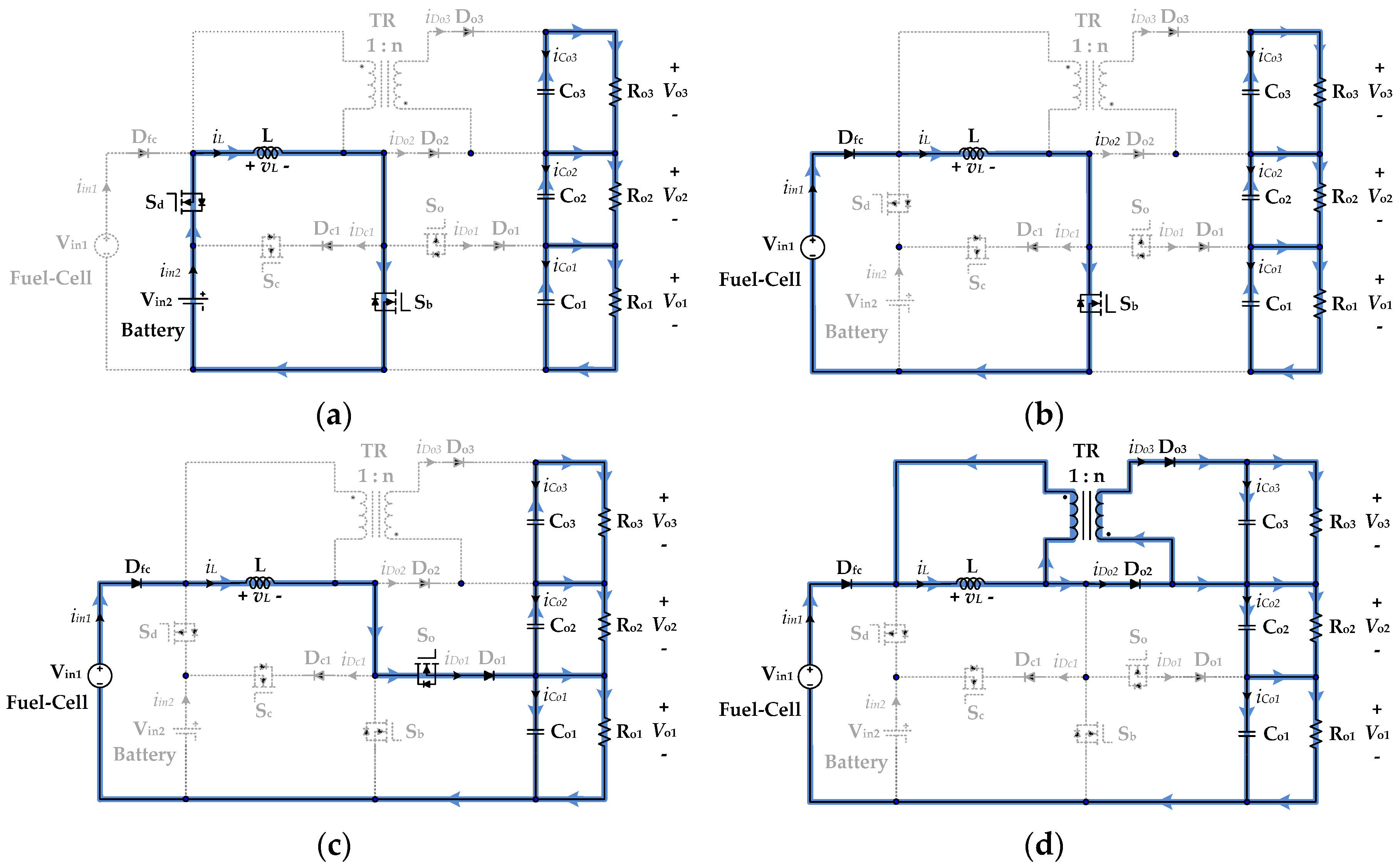
According to the switch states, four operating modes exist in one switching period, as shown in
Figure 3.
State 1 (0 <
t <
DdT): In this state, the switches
Sb,
Sd, and
So are turned on. Because
Sb is turned on, diodes
Do1,
Do2, and
Do3 are reverse-biased, and switch
Sc is turned off. Moreover, because
Sd is turned on and
Vin1 <
Vin2, the diode
Dfc is reverse-biased.
Figure 3a shows the equivalent circuit of the proposed converter in this state.
Vin2 charges the inductor
L, and the inductor current increases linearly. Moreover, the capacitors
Co1–Co3 are discharged and deliver their stored energy to the load resistances
Ro1–Ro3. The inductor and capacitor equations in this state are as follows:
State 2 (
DdT <
t <
DbT): In this state, the switch
Sb is turned on, switch
Sd is turned off, and diodes
Do1,
Do2, and
Do3 are reverse-biased.
Vin1 charges the inductor
L, and the inductor current increases linearly. In addition, the capacitors
Co1–Co3 are discharged and deliver their stored energy to the load resistances
Ro1–Ro3.
Figure 3b shows the equivalent circuit of the proposed converter in this state. The inductor and capacitor equations in this state are as follows:
State 3 (
DbT <
t <
DoT): In this state, the switches
Sb and
Sd are turned off, switch
So is turned on, and diodes
Do2 and
Do3 are reverse-biased. The inductor
L is discharged and delivers the energy to the capacitor
Co1 and load resistance
Ro1; the inductor current decreases linearly. The capacitor
Co1 is charged, and the capacitors
Co2 and
Co3 are discharged and deliver the stored energy to load resistances
Ro2 and
Ro3.
Figure 3c shows the equivalent circuit of the proposed converter in this state. The energy storage element
L and
Co1–Co3 equations in this state are as follows:
State 4 (
DoT <
t <
T): In this state, all switches are turned off. The diode
Do1 is reverse-biased, and diodes
Do2 and
Do3 are forward-biased. The energy stored in the inductor
L is now partly discharged through the ideal transformer and the inductor delivers the stored energy to the capacitors
Co1–Co3 and load resistances
Ro1–Ro3.
Figure 3d shows the equivalent circuit of the proposed converter in this state. The inductor and capacitor equations in this state are as follows:
where
n represents the transformer turn ratio and α and β are the ratios of the inductor current that contributes the energy to load resistances
Ro2 and
Ro3, respectively; that is (α
+ β = 1).
2.2. Battery Charging Mode
In the battery charging mode, Vin1 (FC) not only supplies loads but also supplies power to Vin2 (battery). This condition occurs when the load power is low and the battery must be charged. In this operating mode, switches Sb, Sc, and So are actively switching and switch Sd is turned off. Sb is controlled to regulate total output voltage (Vo1 + Vo2 + Vo3 = VT) to the desired value. The battery charging current is regulated to the desired value by the duty cycle of Sc. Moreover, the output voltage Vo1 is controlled by So. Because of the regulation of VT and Vo1, the output voltages Vo2 and Vo3 are regulated.
Figure 4 shows the gate signals of switches and voltage and current waveforms of the inductor. According to the switch states, four modes exist in one switching period, as shown in
Figure 5.
State 1 (0
< t < DbT): In this state, switch
Sd is turned off; switches
Sb,
Sc, and
So are turned on; and diodes
Do1–
Do3 are reverse-biased.
Vin1 charges the inductor
L, and the inductor current increases linearly. Moreover, the capacitors
Co1–
Co3 are discharged and deliver their stored energy to the load resistances
Ro1–Ro3.
Figure 5a shows the equivalent circuit of the proposed converter in this state. The inductor and capacitor equations in this state are as follows:
State 2 (
DbT < t < DcT): In this state, the switches
Sc and
So are turned on, switches
Sd and
Sb are turned off, and diodes
Do1–
Do3 are reverse-biased. Because
Vin1 <
Vin2 in this state, during this period, the inductor current decreases linearly and the inductor delivers the energy to the battery (
Vin2). Moreover, the capacitors
Co1–Co3 are discharged and deliver their stored energy to the load resistances
Ro1–Ro3.
Figure 5b shows the equivalent circuit of the proposed converter in this state. The inductor and capacitor equations in this mode are as follows:
State 3 (
DcT < t < DoT): In this state, switches
Sd,
Sb, and
Sc are turned off; switch
So is turned on; and diodes
Do2 and
Do3 are reverse-biased. The inductor
L is discharged and delivers the energy to the capacitor
Co1 and load resistance
Ro1; the inductor current decreases linearly. The capacitor
Co1 is charged, and the capacitors
Co2 and
Co3 are discharged and deliver the stored energy to the load resistances
Ro2–Ro3.
Figure 5c shows the equivalent circuit of the proposed converter in this state. The energy storage element
L and
Co1–Co3 equations in this state are as follows:
State 4 (
DoT < t < T): In this state, all the switches are turned off. The diode
Do1 is reverse-biased, and diodes
Do2 and
Do3 are forward-biased. The inductor
L is discharged, and the energy stored in
L is now partly discharged through the ideal transformer to deliver the stored energy to the capacitors
Co1–Co3 and load resistances
Ro1–Ro3.
Figure 5d shows the equivalent circuit of the proposed converter in this state. The inductor and capacitor equations are as follows:
3. Steady-State Analysis
In the battery discharging mode, the energy of the two inputs can be controlled by tuning the duty cycle Dd of the switch Sd. Moreover, the total output voltage (Vo1 + Vo2 + Vo3 = VT) can be regulated to the desired value by tuning the duty cycles Db and Do of the switches Sb and So, respectively. In the battery charging mode, the energy of the input power source Vin1 can be controlled to charge the battery by tuning the duty cycles Db and Dc of the switches Sb and Sc, respectively. Moreover, the total output voltage VT can be regulated to the desired value by tuning the duty cycles Dc and Do of the switches Sc and So, respectively.
According to the voltage-second balance principle and Equations (1)–(4):
Similarly, according to Equations (5)–(8):
According to the equivalent circuits (State 4) of the battery charging and discharging modes, the inductor current delivers the stored energy to load resistances
Ro2 and
Ro3, and the corresponding distributed currents for
Ro2 and
Ro3 can be expressed as follows:
According to Equations (13) and (14):
In summary, the values of the switch duty cycles of the discharging and charging modes are obtained using steady-state equations, which are expressed by Equations (16) and (17), respectively.
4. Simulation and Experimental Results
To verify the performance of the proposed converter, experiments were conducted using a 300-W circuit prototype in battery discharging and charging modes. The corresponding simulation results were also made utilizing the PSIM simulation software [
27]. The parameters are listed in
Table 1. The input voltage sources were
Vin1 = 36 V, and
Vin2 = 48 V. The total output voltage was regulated as
VT-ref =
Vo1-ref + Vo2-ref + Vo3-ref = 300 V ± 10% (
i.e., 270–330 V), and the voltage regulation ranges of the three-output terminals were set to
Vo1-ref =
Vo2-ref = 80 ± 10% (
i.e., 72–88 V) and
Vo3-ref = 140 ± 10% (
i.e., 126–154 V). Moreover, the average battery currents were regulated as
Ib(avg) = 1.4 A and
Ib(avg) = −0.85 A for the battery discharging and charging modes, respectively. The load resistances
Ro1 = 150 Ω,
Ro2 = 75 Ω, and
Ro3 = 75 Ω were used for the battery discharging and charging modes, which are described in
Section 4.1 and
Section 4.2, respectively.
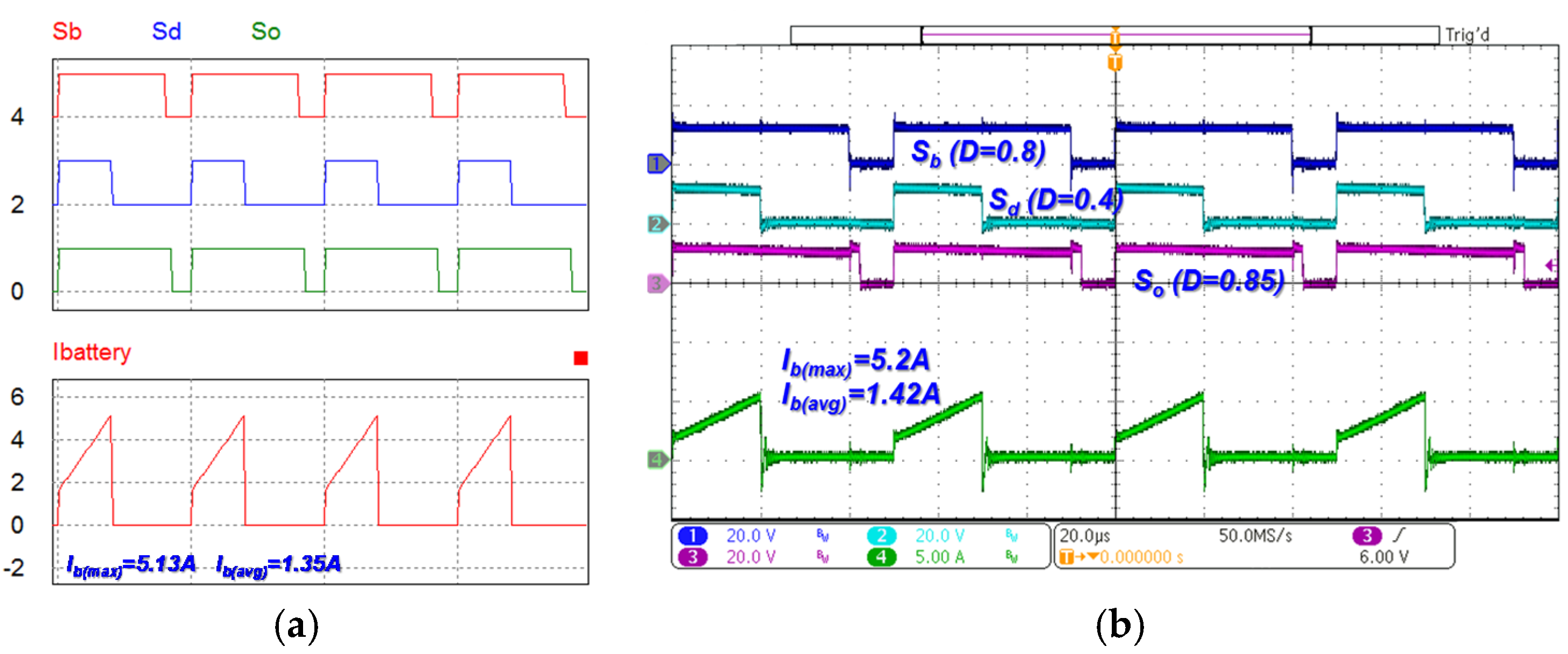
4.1. Battery Discharging Mode
In the battery discharging mode, two input power sources
Vin1 (FC) and
Vin2 (battery) supply the energy to the loads.
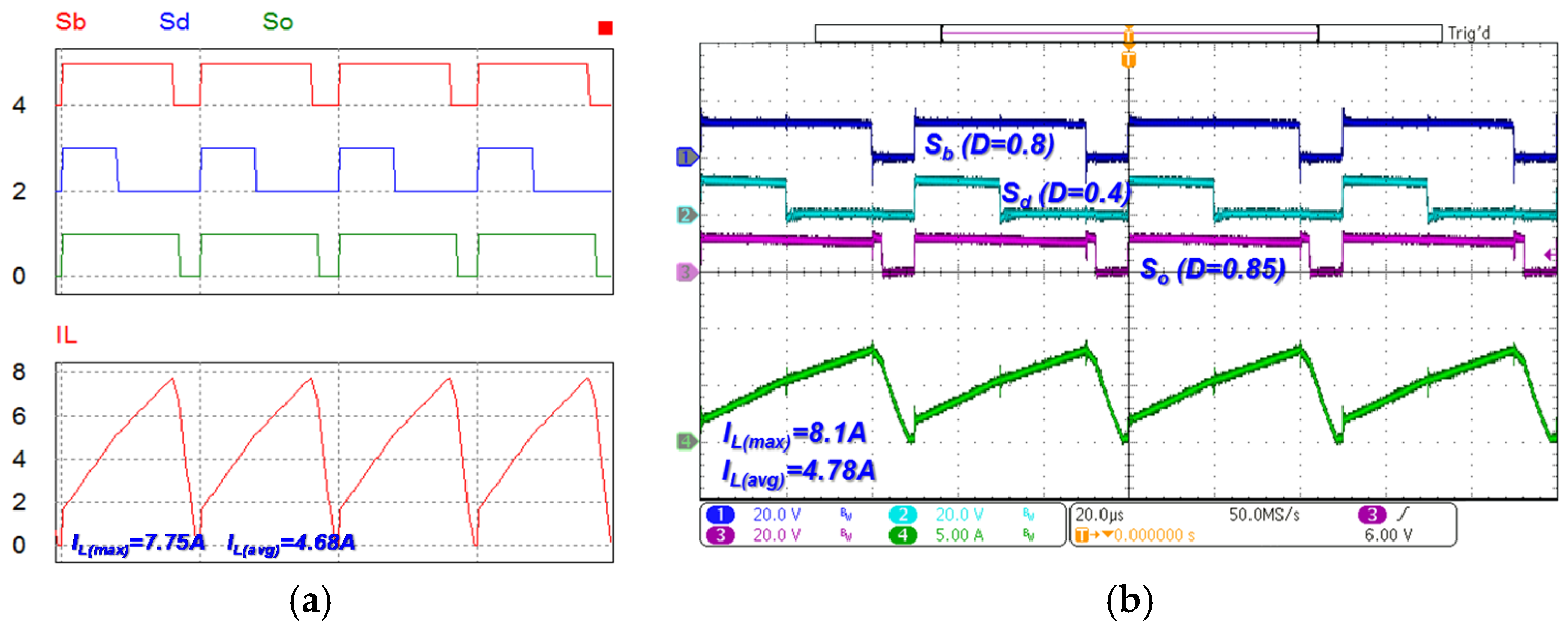
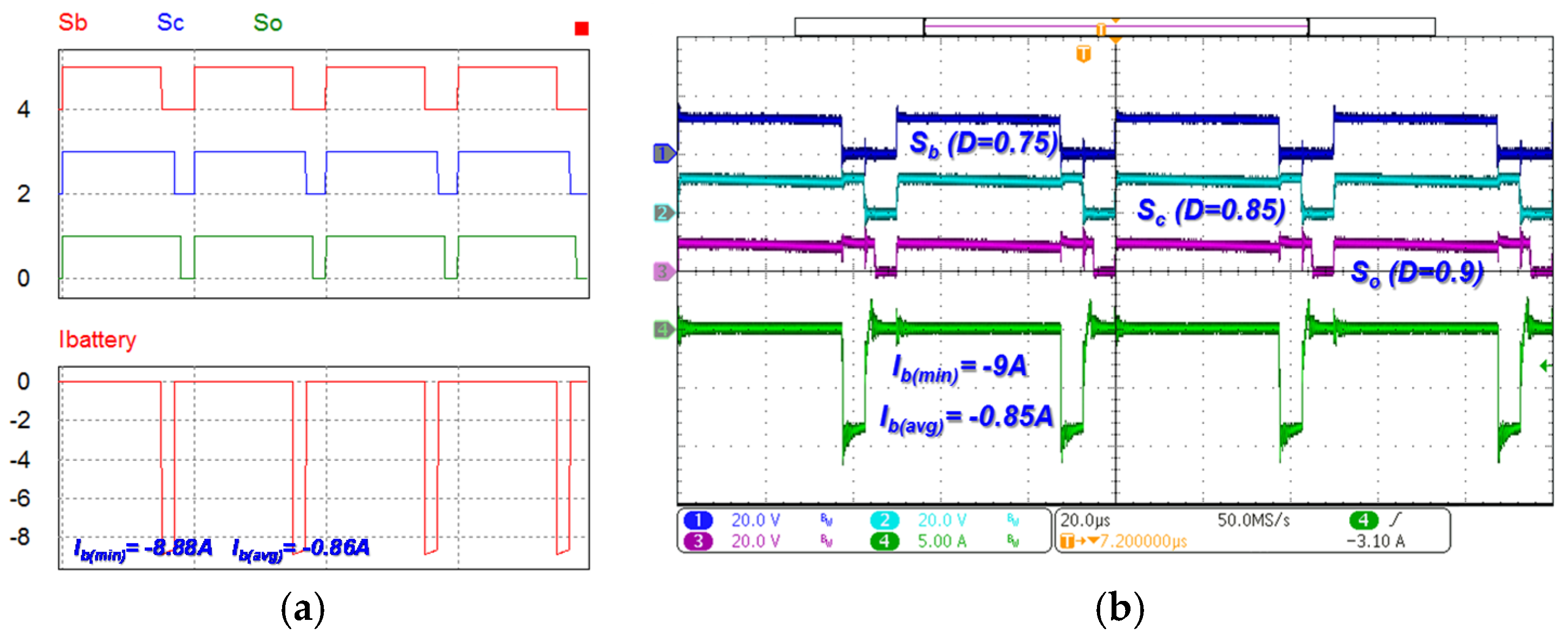
Figure 6 shows the measured waveforms of the switch gate signals and the voltage and current waveforms of the inductor. As shown in this figure, the switch
Sc is turned off, and the switches
Sb,
Sd, and
So are actively controlled. To control the output voltage, the duty cycles
Db and
Do are tuned first, and by tuning the duty cycle
Dd to a higher value, the total output voltage
VT is higher, and
vice versa. As shown in
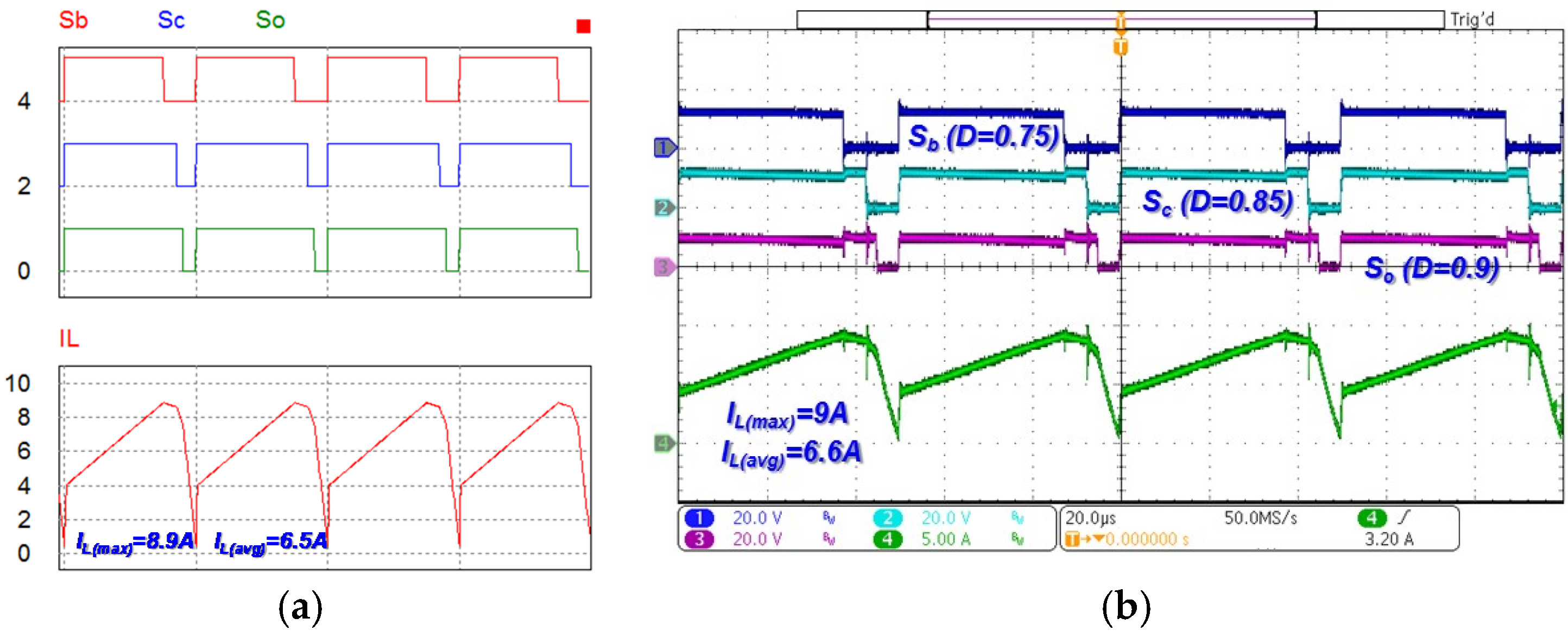
Figure 7, the regulated average battery current
Ib(avg) = 1.42 A and average inductor current
IL(avg) = 4.78 A can be obtained. Notably, the battery current in this mode has a positive value, which implies that the battery has been discharged.
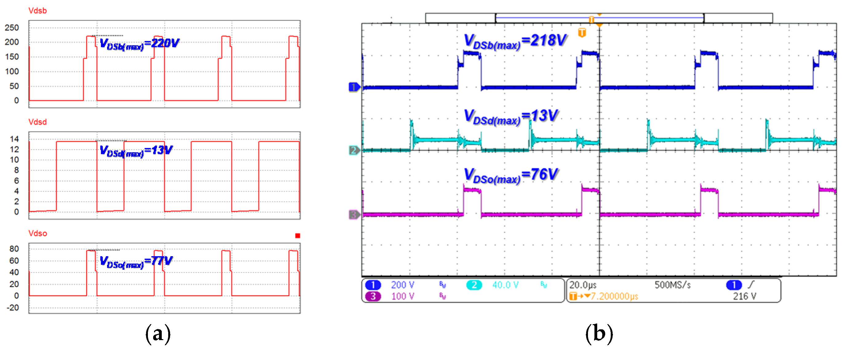
Figure 8 shows both simulation and experimental results of the switch voltages in the battery discharging mode. The maximum voltage stresses of the power switches
Sb,
Sd, and
So are 218 V, 13 V, and 76 V, respectively, which are in close agreement with the corresponding simulation results. All the voltage stresses are lower than the output voltage, and this result enables the adoption of lower voltage rating devices for reducing conduction and switching losses.
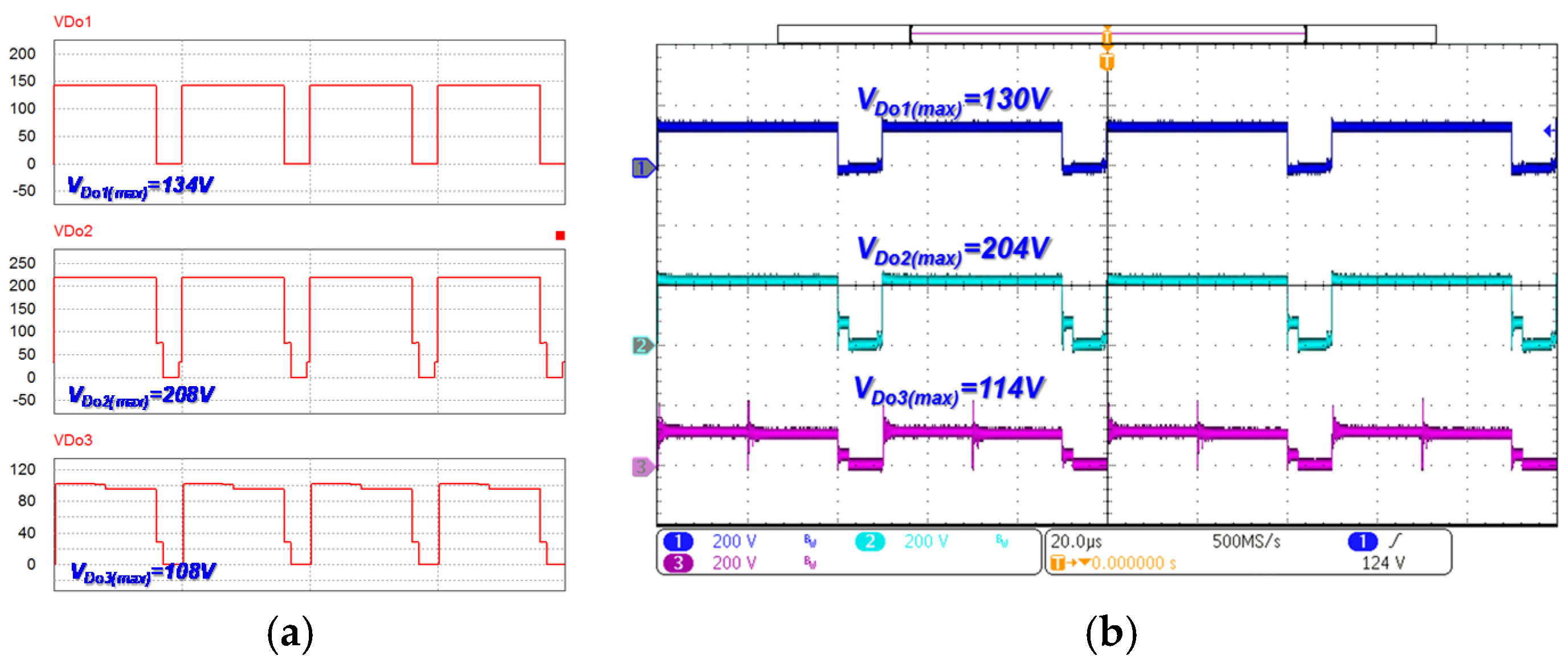
Figure 9 shows the measured waveforms of the diode voltages in the battery discharging mode; the maximum voltage stresses of the diodes
Do1,
Do2, and
Do3 are approximately 130 V, 204 V, and 114 V, respectively. As shown in
Figure 9, both simulation and experimental results are consistent. As shown in
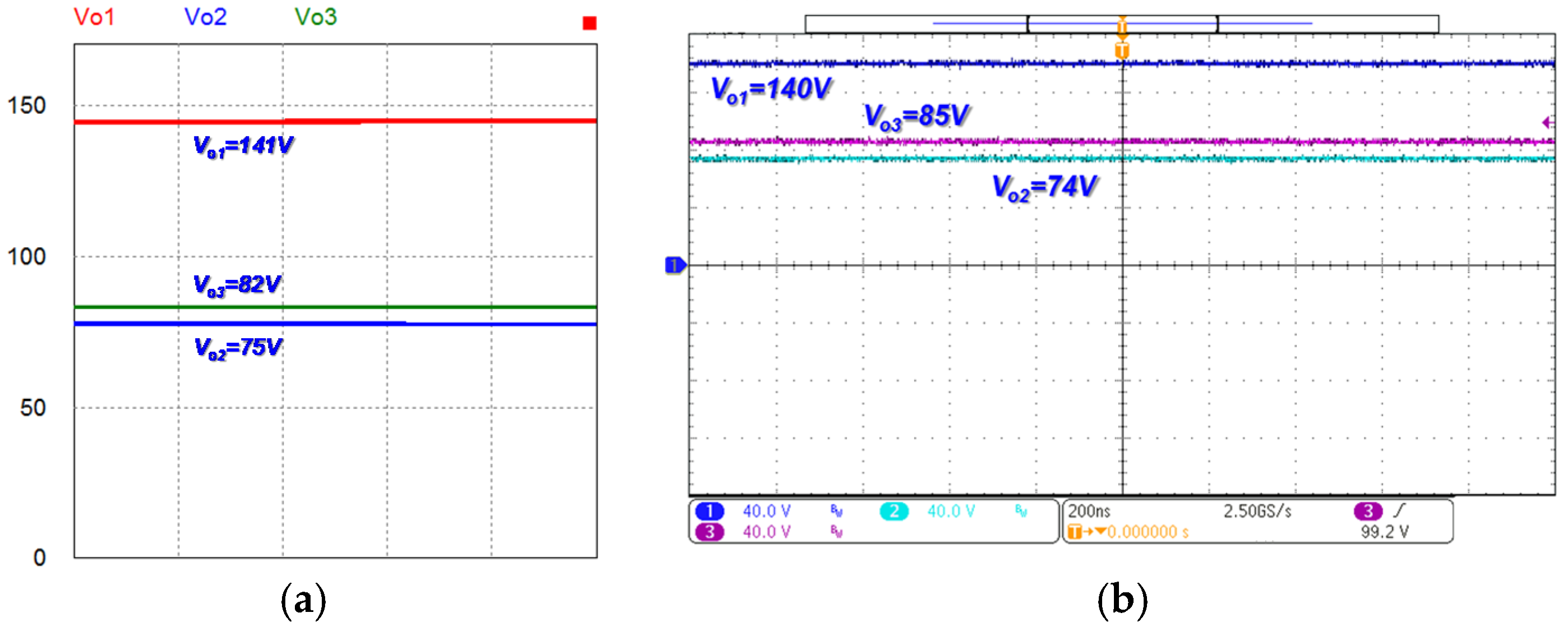
Figure 10, the desired values of the output voltages are
Vo1 = 140 V,
Vo2 = 85 V,
Vo3 = 74 V, and the total output voltage
VT = 299 V. The experimental results are consistent with the circuit simulation results.
4.2. Battery Charging Mode
In the battery charging mode,
Vin1 (FC) not only supplies loads but also delivers power to
Vin2 (battery). This condition occurs when the load power is low and the battery requires to be charged.
Figure 11 shows the measured waveforms of the switch gate signals, and voltage and current waveforms of the inductor. As shown in this figure, the switch
Sd is turned off, and the switches
Sb,
Sc, and
So are actively controlled. As shown in
Figure 12, the regulated average battery current
Ib(avg) = −0.85 A and inductor current
IL(avg) = 6.6 A are obtained. Notably, the battery current in this mode has a negative value, which implies that the battery has been charged.
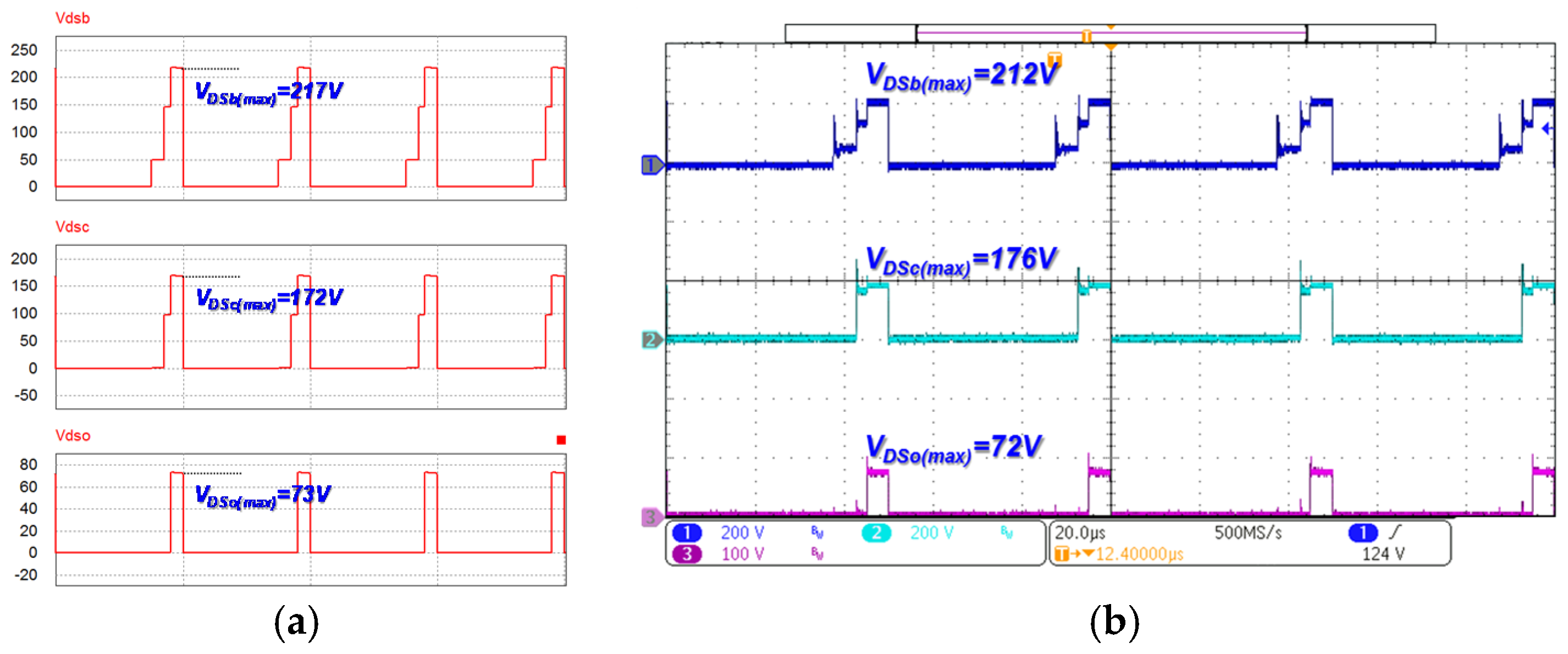
Figure 13 shows both simulation and experimental results of the switch voltages in the battery charging mode. The maximum voltage stresses of the power switches
Sb,
Sc, and
So are 212 V, 176 V, and 72 V, respectively, which are in close agreement with the corresponding simulation results.
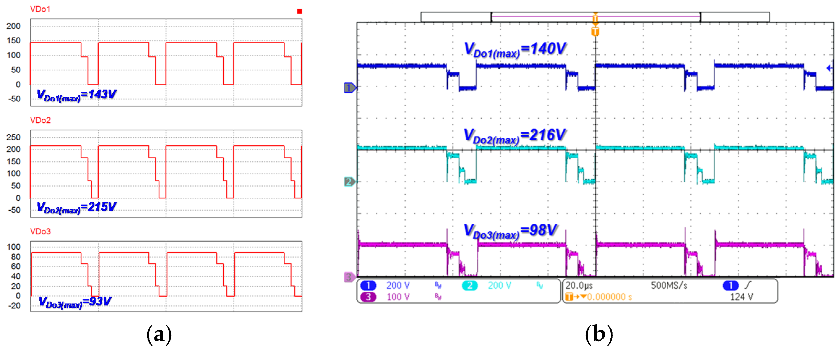
Figure 14 shows the measured waveforms of the diode voltages in the battery charging mode; the maximum voltage stresses of the diodes
Do1,
Do2, and
Do3 are approximately 140 V, 216 V, and 98 V, respectively. Both the simulation and experimental results are in close agreement as well. As shown in
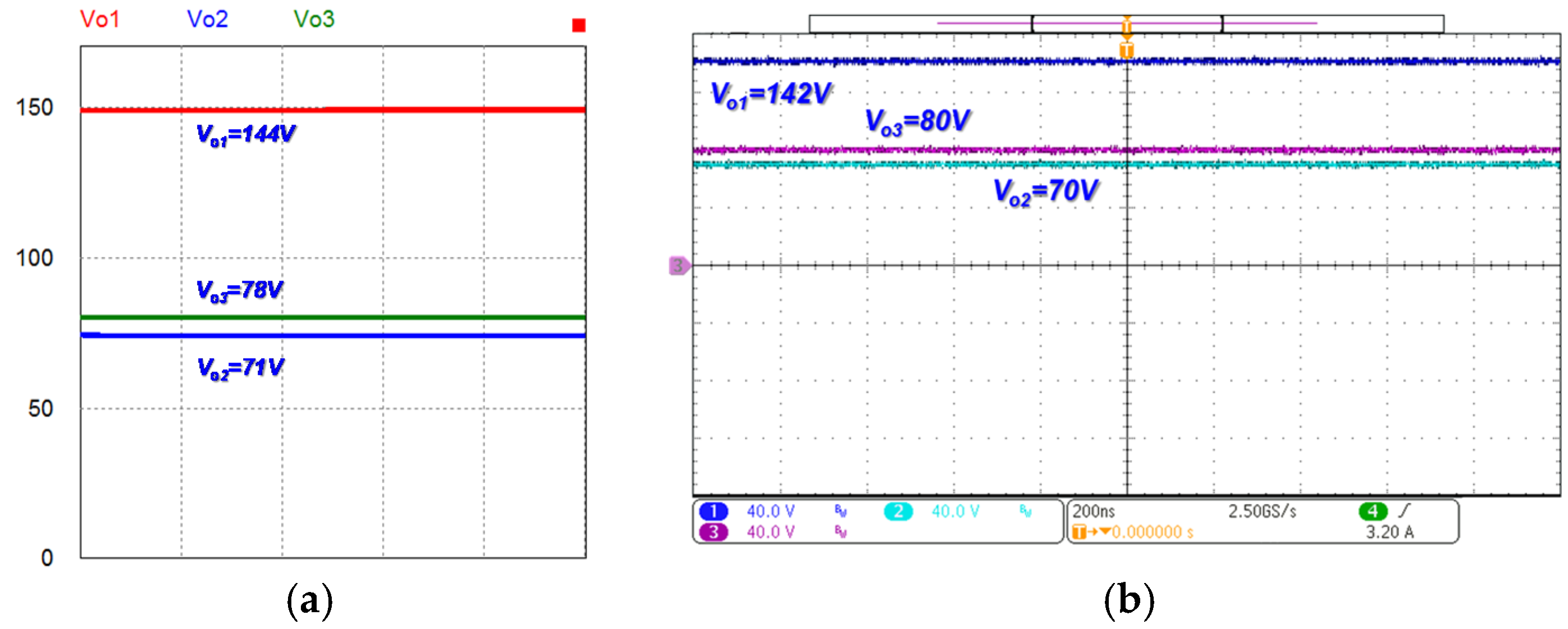
Figure 15, the three-output voltages are
Vo1 = 142 V,
Vo2 = 80 V,
Vo3 = 70 V, and the total output
VT = 292 V. These results are in the voltage regulation range as expected.
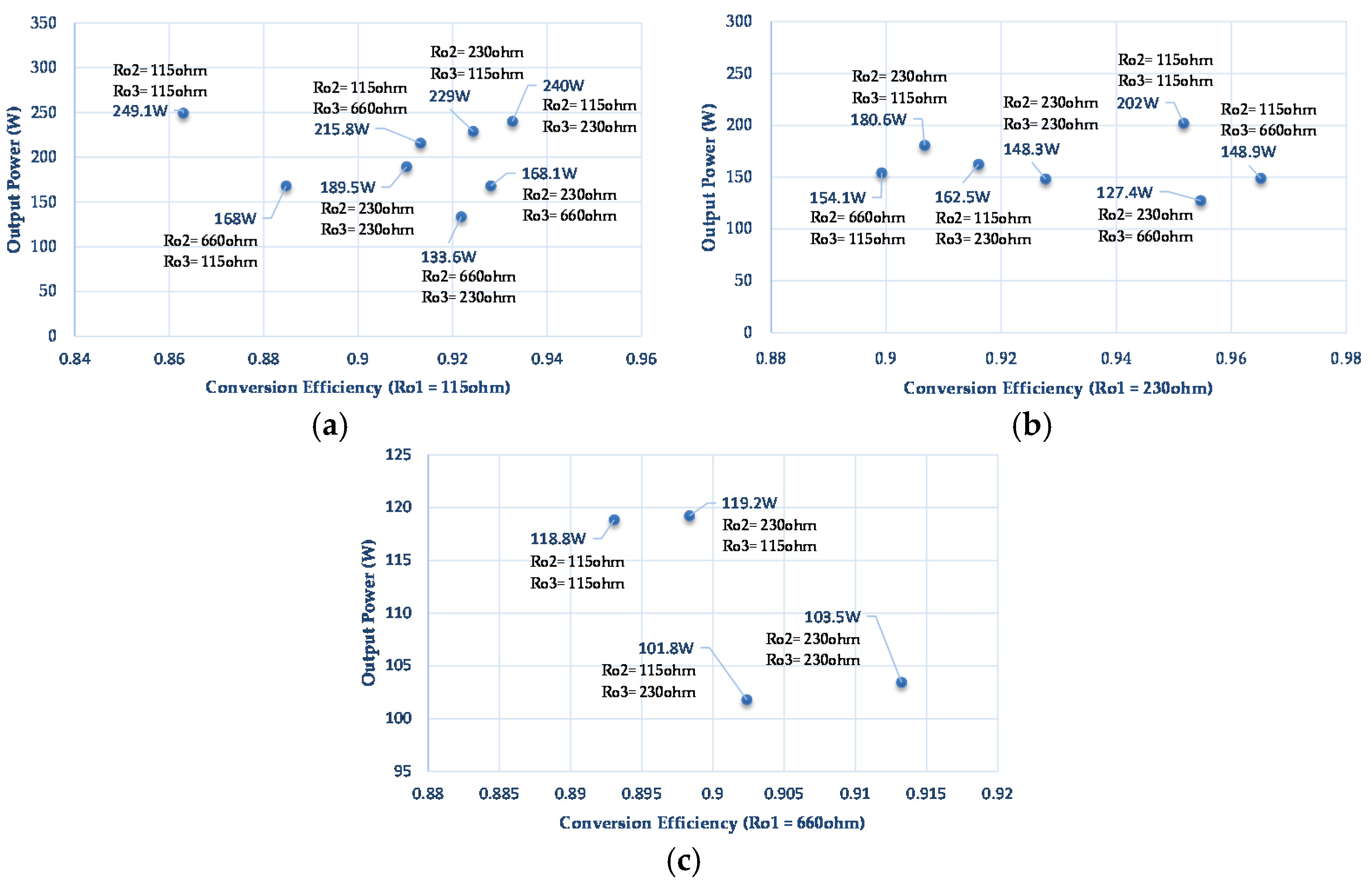
Figure 16 shows the measured conversion efficiency for different load conditions in the battery discharging mode. The conversion efficiency was measured using a digital power meter (Yokogawa-WT310, Tokyo, Japan). As shown in
Figure 16, the measured highest conversion efficiency was as high as 96.6% at half-load output. In this condition, the load resistances are set as
Ro1 = 230 Ω,
Ro2 = 115 Ω, and
Ro3 = 660 Ω.
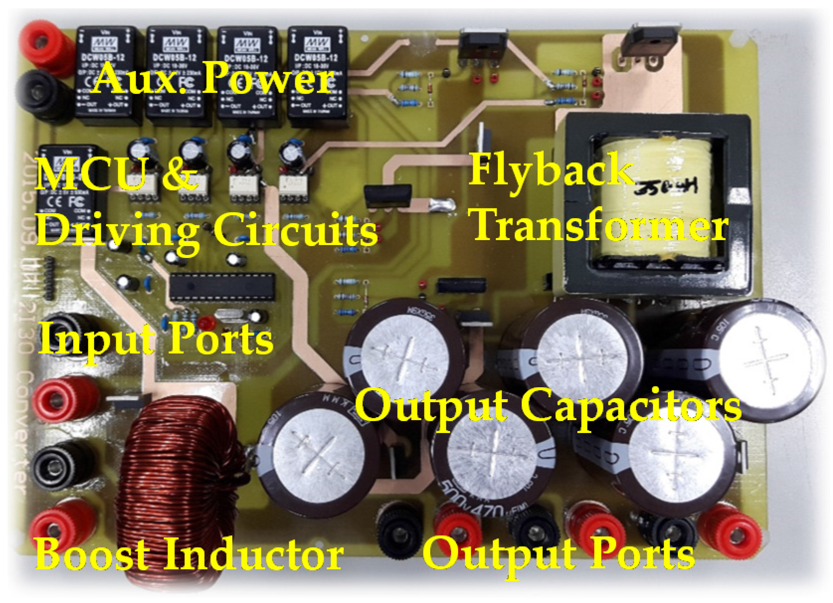
Figure 17 shows the image of the realized prototype for reference.


