GaN HEMTs for Electric Vehicle Power Electronics: Device Architectures, Reliability and Next-Generation Wide Bandgap Opportunities


Abstract
1. Introduction
2. Evolution of Power Semiconductors in EVs
2.1. Silicon: The Industry Standard with Fundamental Limits
2.2. Silicon Carbide: The First Wide Bandgap Breakthrough
2.3. Gallium Nitride: Toward Compact and High-Frequency EV Power Electronics
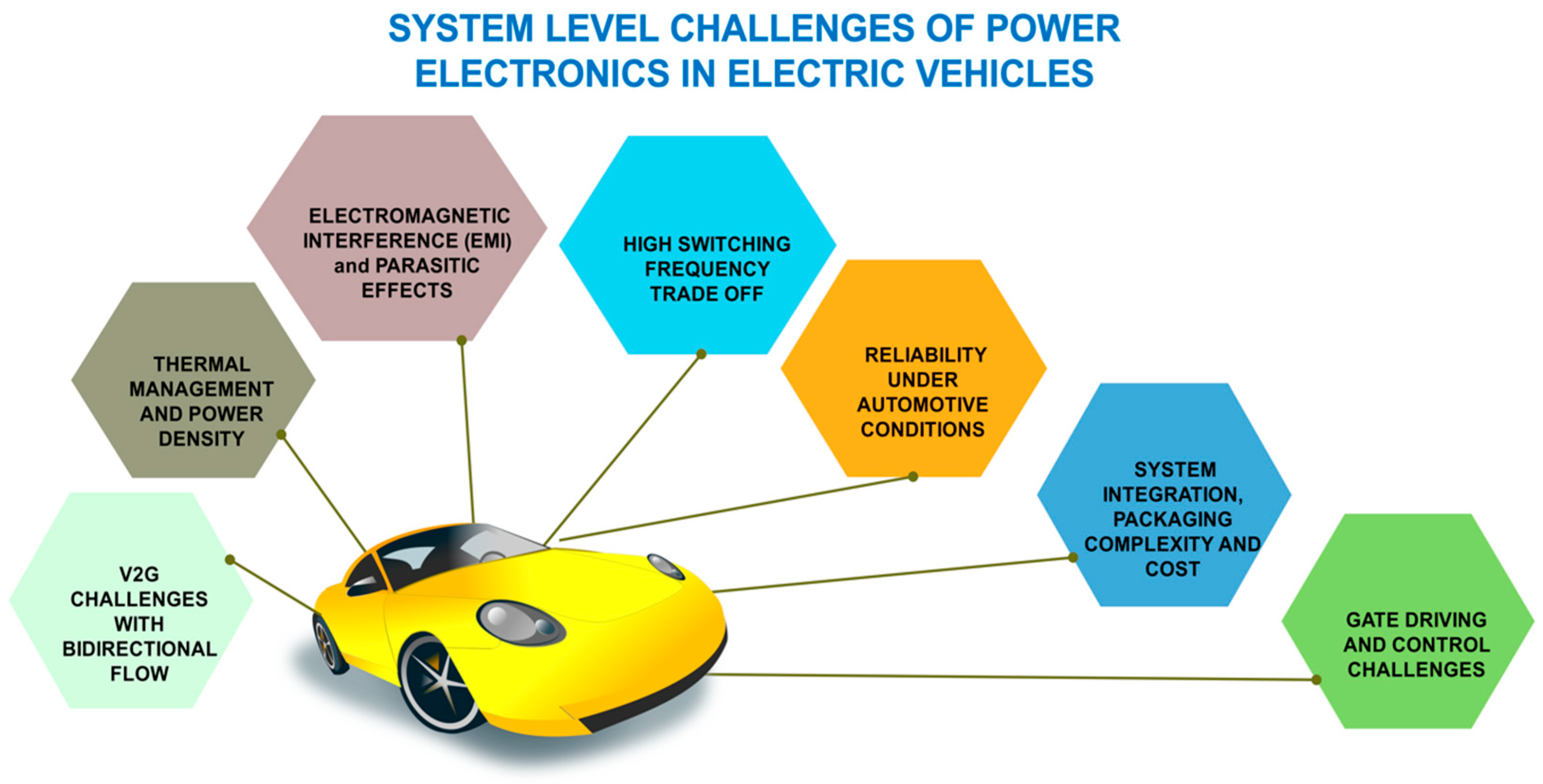
3. System-Level Challenges of Power Electronics in Electric Vehicles
3.1. Thermal Management and Power Density
3.2. Efficiency Versus Switching Frequency Trade-Off
3.3. Electromagnetic Interference (EMI) and Parasitic Effects
3.4. Reliability Under Automotive Conditions
3.5. System Integration, Packaging Complexity and Cost
3.6. Gate Driving and Control Challenges
3.7. Challenges of Bidirectional Power Flow in V2G-Enabled EVs
4. GaN HEMT Structures for Power Electronics
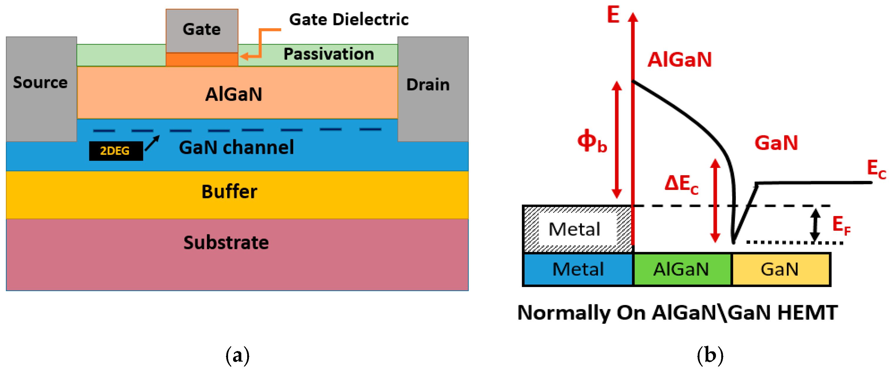
4.1. Normally on GaN HEMT (Depletion Mode)
4.2. Enhancement Mode (E-Mode, Normally Off) GaN HEMT
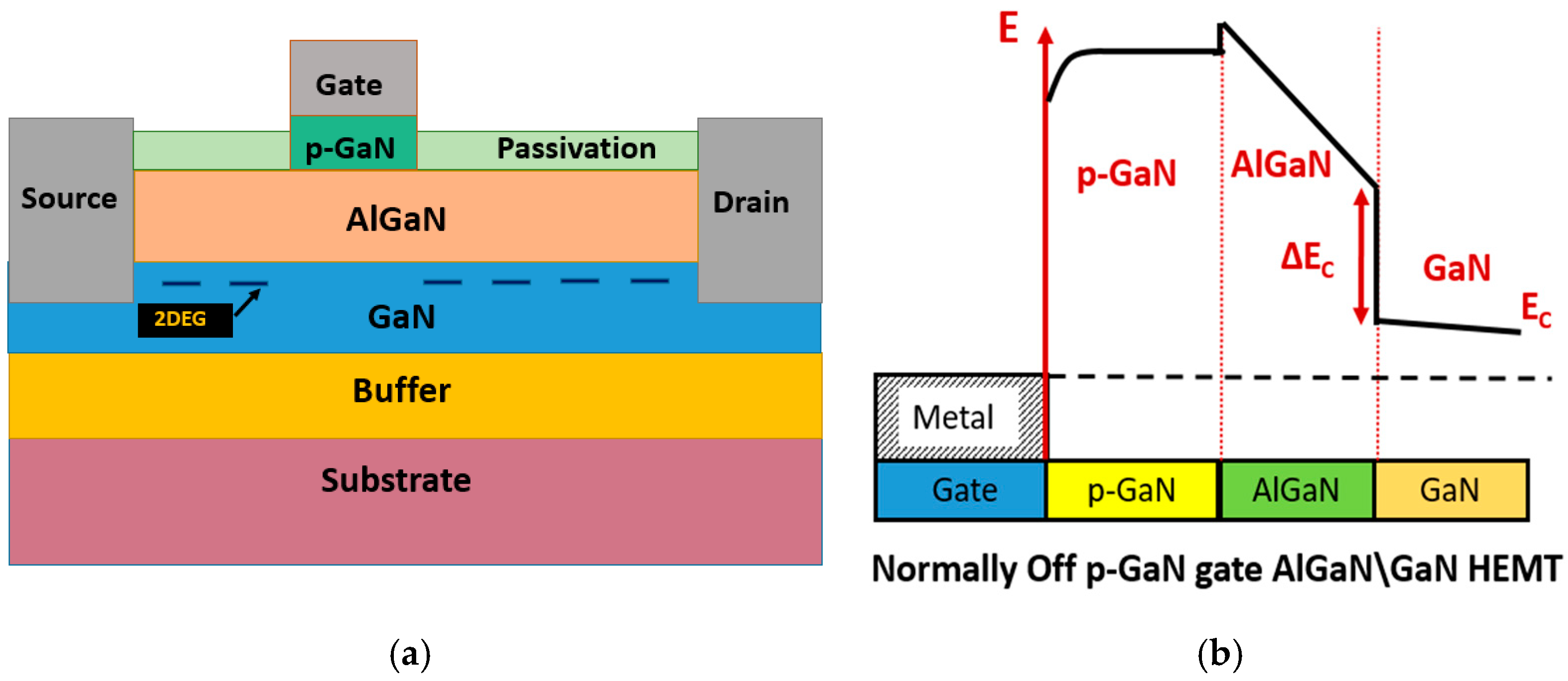
4.2.1. p-GaN Gate HEMT
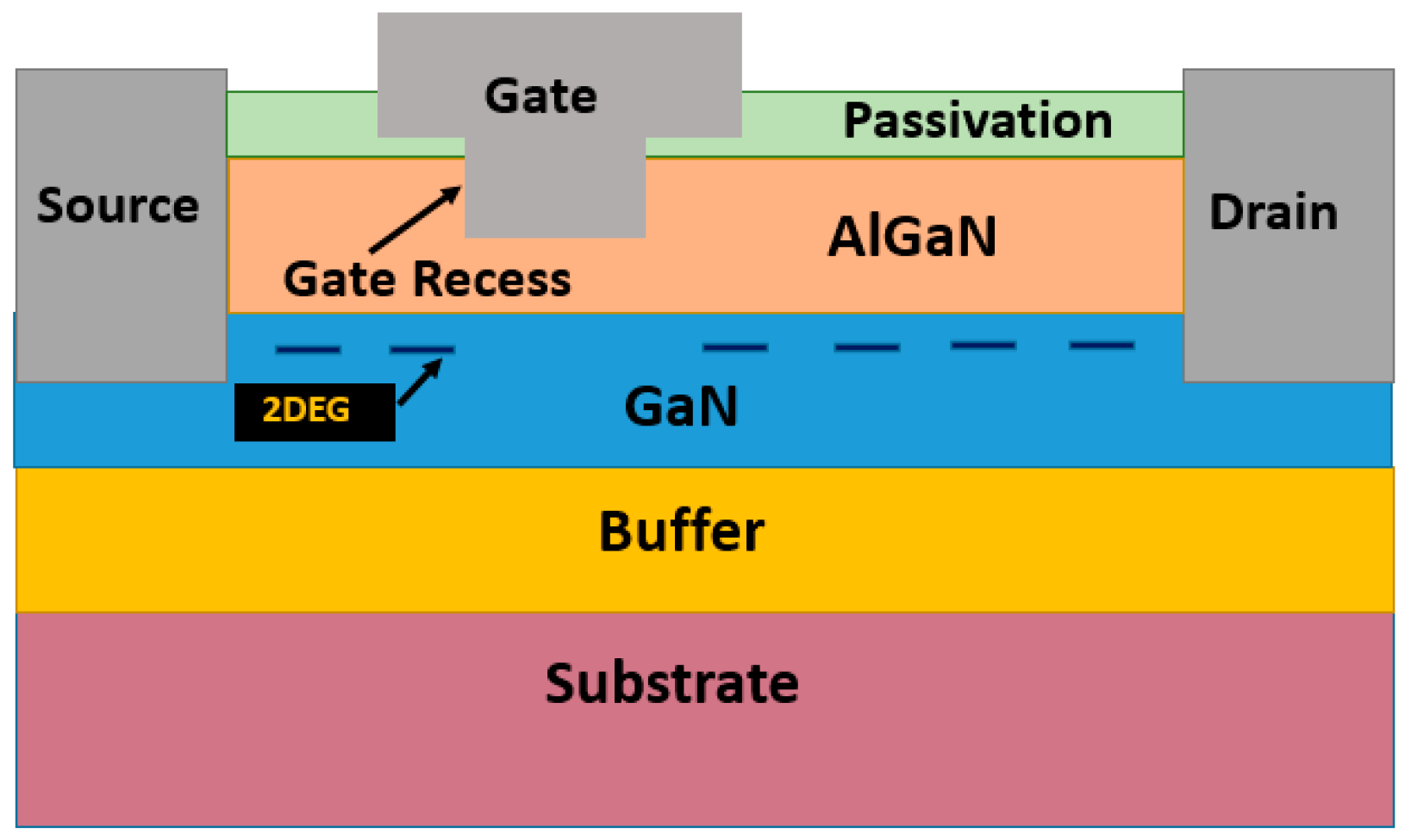
4.2.2. Gate Recess HEMT
4.2.3. Cascode GaN HEMT
4.3. Advanced Barrier/Buffer Design
4.3.1. High-Al-Content AlGaN Barriers
4.3.2. Superlattice Buffer
4.3.3. Polarization-Engineered Back Barrier
4.4. Substrate Engineered GaN HEMT
4.4.1. GaN-on-Si
4.4.2. GaN-on-SiC
4.4.3. GaN-on-GaN
4.4.4. GaN-on-QST
4.4.5. GaN-on-Diamond
5. State-of-the-Art GaN Discrete Devices and Automotive Qualification
5.1. Commercial and Emerging GaN HEMTs for EV Power Electronics
5.2. Standardization and Qualification Frameworks for Automotive GaN HEMTs
6. Reliability and Operational Challenges of GaN HEMTs in EV Applications
6.1. Device-Level Challenges and Reliability Issues
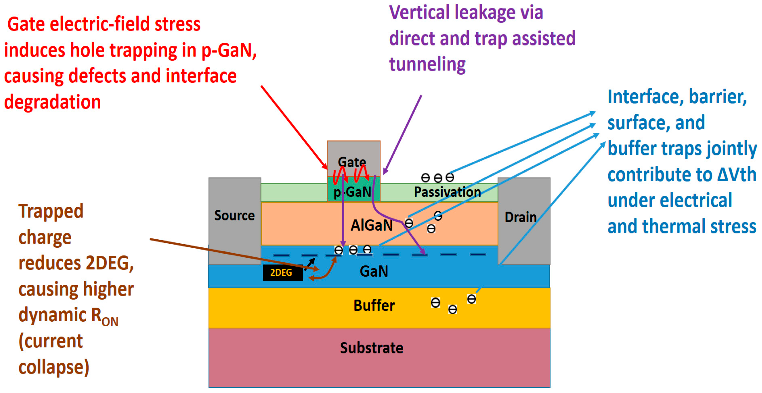
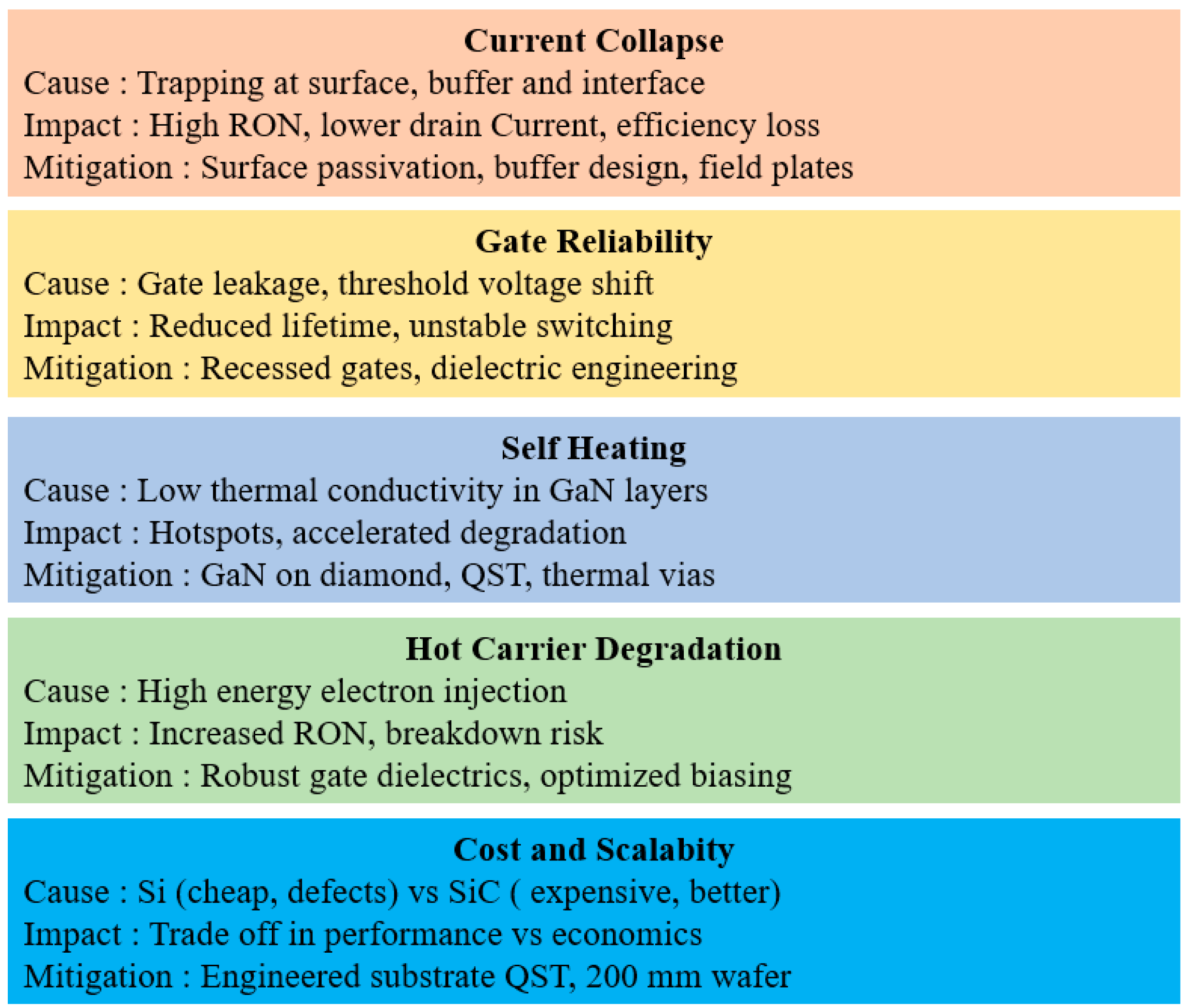
6.1.1. Current Collapse and Trapping Effects
6.1.2. Gate Reliability and Gate Leakage
6.1.3. Self-Heating and Thermal Management
6.1.4. Hot Carrier Degradation
6.1.5. Cost, Substrate, and Scalability Trade-Offs
6.2. Impact of Realistic EV Operating Condition on GaN HEMT
7. Ultra-Wide-Bandgap Semiconductors: Opportunities Beyond GaN
8. Open Challenges and Future Research Opportunities
9. Conclusions
Author Contributions
Funding
Data Availability Statement
Acknowledgments
Conflicts of Interest
Abbreviations
| ALE | Atomic Layer Etching |
| DLTS | Deep-Level Transient Spectroscopy |
| EV | Electric Vehicle |
| HEV | Hybrid Electric Vehicle |
| HEMT | High-Electron-Mobility Transistor |
| HTRB | High-Temperature Reverse Bias |
| IL | Interlayer |
| NERT | National Energy Transition Roadmap |
| NIMP | New Industrial Master Plan |
| OBC | On-Board Charger |
| ICE | Internal Combustion Engine |
| IGBT | Insulated Gate Bipolar Transistor |
| MIS | Metal Insulator Semiconductor |
| MOSFET | Metal–Oxide–Semiconductor Field-Effect Transistor |
| LCMB | Low Carbon Mobility Blueprint |
| SL | Superlattice |
| SDG | Sustainable Development Goal |
| WBG | Wide Bandgap |
| 2DEG | Two-Dimensional Electron Gas |
| EMI | Electromagnetic Interference |
| OEM | Original Equipment Manufacturer |
| CMTI | Common Mode Transient Immunity |
| BD | Break Down |
| BTI | Bias Temperature Instability |
| h-BN | Hexagonal Boron Nitride |
| TAT | Trap-Assisted Tunneling |
| TBR | Thermal Boundary Resistance |
| TCAD | Technology Computer-Aided Design |
| UIS | Unclamped Inductive Switching |
| UWBG | Ultra-Wide Bandgap |
| QST | Qromis Substrate Technology |
References
- Fesli, U.; Ozdemir, M.B. Electric Vehicles: A Comprehensive Review of Technologies, Integration, Adoption, and Optimization. IEEE Access 2024, 12, 140908–140931. [Google Scholar] [CrossRef]
- Acharige, S.S.G.; Haque, M.E.; Arif, M.T.; Hosseinzadeh, N.; Hasan, K.N.; Oo, A.M.T. Review of Electric Vehicle Charging Technologies, Standards, Architectures, and Converter Configurations. IEEE Access 2023, 11, 41218–41255. [Google Scholar] [CrossRef]
- Abdelsattar, M.; Ismeil, M.A.; Aly, M.M.; Abu-Elwfa, S.S. Analysis of Renewable Energy Sources and Electrical Vehicles Integration into Microgrid. IEEE Access 2024, 12, 66822–66832. [Google Scholar] [CrossRef]
- Yousuf, A.K.M.; Wang, Z.; Paranjape, R.; Tang, Y. An In-Depth Exploration of Electric Vehicle Charging Station Infrastructure: A Comprehensive Review of Challenges, Mitigation Approaches, and Optimization Strategies. IEEE Access 2024, 12, 51570–51589. [Google Scholar] [CrossRef]
- Rana, M.M.; Alam, S.M.; Rafi, F.A.; Deb, S.B.; Agili, B.; He, M.; Ali, M.H. Comprehensive Review on the Charging Technologies of Electric Vehicles (EV) and Their Impact on Power Grid. IEEE Access 2025, 13, 35124–35156. [Google Scholar] [CrossRef]
- Iannaccone, G.; Sbrana, C.; Morelli, I.; Strangio, S. Power Electronics Based on Wide-Bandgap Semiconductors: Opportunities and Challenges. IEEE Access 2021, 9, 139446–139456. [Google Scholar] [CrossRef]
- Keshmiri, N.; Wang, D.; Agrawal, B.; Hou, R.; Emadi, A. Current Status and Future Trends of GaN HEMTs in Electrified Transportation. IEEE Access 2020, 8, 70553–70571. [Google Scholar] [CrossRef]
- Okhueleigbe, V.O.; Bello, A.Y. An Overview of Integrating Power Electronic Systems and Advanced Control Methods for Ultra-Fast Electric Vehicle (EV) Charging Stations in Independent Microgrids. Path Sci. 2025, 11, 2001–2008. [Google Scholar] [CrossRef]
- Sahu, S.K.; Chacko, S.T.; Parmar, O.; Rajput, A.S. Wide Bandgap Materials: Revitalizing Power Electronics with Advances in Power Semiconductor Devices. J. Inst. Eng. India Ser. B 2025, 106, 1287–1303. [Google Scholar] [CrossRef]
- Zhang, B.; Zhang, W. The Present Status and Future Developments of Si-Based Power Semiconductor Technologies: “More Silicon” Development in Power Semiconductors Still Possesses Robust Vitality. IEEE Electron Devices Mag. 2024, 2, 8–15. [Google Scholar] [CrossRef]
- Lee, H.; Smet, V.; Tummala, R. A Review of SiC Power Module Packaging Technologies: Challenges, Advances, and Emerging Issues. IEEE J. Emerg. Sel. Top. Power Electron. 2020, 8, 239–255. [Google Scholar] [CrossRef]
- Han, L.; Tang, X.; Wang, Z.; Gong, W.; Zhai, R.; Jia, Z.; Zhang, W. Research Progress and Development Prospects of Enhanced GaN HEMTs. Crystals 2023, 13, 911. [Google Scholar] [CrossRef]
- Kumar, J.S.R.; John, H.V.D.; I.V., B.K.; Ajayan, J. A Comprehensive Review of AlGaN/GaN High Electron Mobility Transistors: Architectures and Field Plate Techniques for High Power/High Frequency Applications. Microelectron. J. 2023, 140, 105951. [Google Scholar] [CrossRef]
- Omar, A.; Loan, S.A. Polarization Engineered Design for Normally-Off, Higher Drain Current and Higher Breakdown Voltage Gan-Based MOS-HEMT. ACS Omega 2025, 10, 62854–62863. [Google Scholar] [CrossRef]
- Li, N.D.; Lin, Y.C.; Chen, K.W.; Hsu, H.T.; Tsao, Y.F.; Chang, E.Y. Novel Gate Fabrication Process Enhancing High-Frequency Operation in AlGaN/GaN HEMTs for Ka-Band Applications. IEEE J. Electron Devices Soc. 2025, 13, 593–598. [Google Scholar] [CrossRef]
- Kozak, J.P.; Zhang, R.; Porter, M.; Song, Q.; Liu, J.; Wang, B.; Wang, R.; Saito, W.; Zhang, Y. Stability, Reliability, and Robustness of GaN Power Devices: A Review. IEEE Trans. Power Electron. 2023, 38, 8442–8471. [Google Scholar] [CrossRef]
- Han, G.; Kim, J.; Park, S.; Bae, W. Thermal Management of Wide-Bandgap Power Semiconductors: Strategies and Challenges in SiC and GaN Power Devices. Electronics 2025, 14, 4193. [Google Scholar] [CrossRef]
- Tran, M.T.; Deepak, K.; Martin, G.E.; Bay, O.; El Baghdadi, M.; Hegazy, O. A High-Performance GaN Power Module with Parallel Packaging for High-Current and Low-Voltage Traction Inverter Applications. IEEE J. Emerg. Sel. Top. Power Electron. 2025, 13, 1188–1209. [Google Scholar] [CrossRef]
- Zhu, L.; Bai, H.; Brown, A.; McAmmond, M. Transient Analysis When Applying GaN + Si Hybrid Switching Modules to a Zero-Voltage-Switching EV Onboard Charger. IEEE Trans. Transp. Electrif. 2020, 6, 146–157. [Google Scholar] [CrossRef]
- Zhao, S.; Kempitiya, A.; Chou, W.T.; Palija, V.; Bonfiglio, C. Variable DC-Link Voltage LLC Resonant DC/DC Converter with Wide Bandgap Power Devices. IEEE Trans. Ind. Appl. 2022, 58, 2965–2977. [Google Scholar] [CrossRef]
- Emon, A.I.; Mustafeez-ul-Hassan; Mirza, A.B.; Kaplun, J.; Vala, S.S.; Luo, F. A Review of High-Speed GaN Power Modules: State of the Art, Challenges, and Solutions. IEEE J. Emerg. Sel. Top. Power Electron. 2023, 11, 2707–2729. [Google Scholar] [CrossRef]
- Kizilyalli, I.C.; Carlson, E.P.; Cunningham, D.W.; Manser, J.S.; Xu, Y.; Liu, A.Y. Wide Band-Gap Semiconductor Based Power Electronics for Energy Efficiency; U.S. Department of Energy: Washington, DC, USA, 2018.
- Wellmann, P. Power Electronic Semiconductor Materials for Automotive and Energy Saving Applications—SiC, GaN, Ga2O3, and Diamond. Z. Anorg. Allg. Chem. 2017, 643, 1312–1322. [Google Scholar] [CrossRef] [PubMed]
- Garrido-Diez, D.; Baraia, I. Review of Wide Bandgap Materials and Their Impact in New Power Devices. In Proceedings of the IEEE International Workshop ECMSM, Donostia-San Sebastian, Spain, 24–26 May 2017; pp. 1–6. [Google Scholar]
- Cittanti, A.D.; Vico, E.; Bojoi, I.R. New FOM-Based Performance Evaluation of 600/650 V SiC and GaN Semiconductors for Next-Generation EV Drives. IEEE Access 2022, 10, 51693–51707. [Google Scholar] [CrossRef]
- Garg, T.; Kale, S. Recent developments, reliability issues, challenges and applications of GaN HEMT technology. IEEE Electron. Devices Rev. 2024, 1, 16–30. [Google Scholar] [CrossRef]
- Malaysian Green Technology and Climate Change Corporation. Low Carbon Mobility Blueprint (LCMB). Available online: https://www.mgtc.gov.my/what-we-do/low-carbon-mobility-2/low-carbon-mobility-blueprint/ (accessed on 18 February 2026).
- Shahrilmd. Powering the Future: Accelerating Malaysia’s EV Charging Revolution for Sustainable Mobility. MIDA—Malaysian Investment Development Authority. Available online: https://www.mida.gov.my/powering-the-future-accelerating-malaysias-ev-charging-revolution-for-sustainable-mobility/ (accessed on 18 February 2026).
- Muzir, N.A.Q.; Mojumder, M.R.H.; Hasanuzzaman, M.; Selvaraj, J. Challenges of electric vehicles and their prospects in Malaysia: A comprehensive review. Sustainability 2022, 14, 8320. [Google Scholar] [CrossRef]
- Adesivi “Vietato Fumare”—Set da 10 (5 cm, Resistenti UV). Available online: https://malaysiaindicator.com/roadblocks-to-revolution-the-challenges-of-electric-vehicle-adoption-in-malaysia/ (accessed on 18 February 2026).
- Ming, C. Challenges and Opportunities Lay in Malaysia’s Electric Vehicle Market. Focus Malaysia—Business & Beyond. Available online: https://focusmalaysia.my/challenges-and-opportunities-lay-in-malaysias-electric-vehicle-market/ (accessed on 18 February 2026).
- Liu, A.-C.; Tu, P.-T.; Langpoklakpam, C.; Huang, Y.-W.; Chang, Y.-T.; Tzou, A.-J.; Hsu, L.-H.; Lin, C.-H.; Kuo, H.-C.; Chang, E.Y. The Evolution of Manufacturing Technology for GaN Electronic Devices. Micromachines 2021, 12, 737. [Google Scholar] [CrossRef]
- Panchanathan, S.; Vishnuram, P.; Rajamanickam, N.; Bajaj, M.; Blazek, V.; Prokop, L.; Misak, S. A Comprehensive Review of the Bidirectional Converter Topologies for the Vehicle-to-Grid System. Energies 2023, 16, 2503. [Google Scholar] [CrossRef]
- Khalid, M.R.; Khan, I.A.; Hameed, S.; Asghar, M.S.J.; Ro, J.-S. A Comprehensive Review on Structural Topologies, Power Levels, Energy Storage Systems, and Standards for Electric Vehicle Charging Stations and Their Impacts on Grid. IEEE Access 2021, 9, 128069–128094. [Google Scholar] [CrossRef]
- Barman, P.; Dutta, L.; Bordoloi, S.; Kalita, A.; Buragohain, P.; Bharali, S.; Azzopardi, B. Renewable energy integration with electric vehicle technology: A review of the existing smart charging approaches. Renew. Sustain. Energy Rev. 2023, 183, 113518. [Google Scholar] [CrossRef]
- Amry, Y.; Elbouchikhi, E.; Le Gall, F.; Ghogho, M.; El Hani, S. Electric Vehicle Traction Drives and Charging Station Power Electronics: Current Status and Challenges. Energies 2022, 15, 6037. [Google Scholar] [CrossRef]
- Roccaforte, F.; Greco, G.; Fiorenza, P.; Iucolano, F. An Overview of Normally-Off GaN-Based High Electron Mobility Transistors. Materials 2019, 12, 1599. [Google Scholar] [CrossRef]
- Power GaN 2021: Epitaxy, Devices, Application and Technology Trends Report. 2021. Available online: https://medias.yolegroup.com/uploads/2021/05/YINTR21190_GaN_Power_May2021_Sample.pdf (accessed on 18 February 2026).
- Gachovska, T.K.; Hudgins, J.L. SiC and GaN power semiconductor devices. In Power Electronics Handbook; Butterworth-Heinemann: Burlington, MA, USA, 2018; pp. 95–155. [Google Scholar]
- Li, S.; Lu, S.; Mi, C.C. Revolution of Electric Vehicle Charging Technologies Accelerated by Wide Bandgap Devices. Proc. IEEE 2021, 109, 985–1003. [Google Scholar] [CrossRef]
- Buffolo, M.; Favero, D.; Marcuzzi, A.; De Santi, C.; Meneghesso, G.; Zanoni, E.; Meneghini, M. Review and Outlook on GaN and SiC Power Devices: Industrial State-of-the-Art, Applications, and Perspectives. IEEE Trans. Electron Devices 2024, 71, 1344–1355. [Google Scholar] [CrossRef]
- Alatise, O.; Deb, A.; Bashar, E.; Gonzalez, J.O.; Jahdi, S.; Issa, W. A Review of Power Electronic Devices for Heavy Goods Vehicles Electrification: Performance and Reliability. Energies 2023, 16, 4380. [Google Scholar] [CrossRef]
- Wilson, P. International Technology Roadmap for Wide Bandgap Power Semiconductors: A Five Year Review [Expert View]. IEEE Power Electron. Mag. 2025, 12, 108–111. [Google Scholar] [CrossRef]
- Wang, H.; Hu, J.; De Doncker, R.W. Guest editorial special section on advancing power electronics reliability: Components, systems, and intelligent operation. IEEE J. Mag. 2024, 39, 14216–14217. [Google Scholar]
- Zhong, Y.; Zhang, J.; Wu, S.; Jia, L.; Yang, X.; Liu, Y.; Zhang, Y.; Sun, Q. A review on the GaN-on-Si power electronic devices. Fundam. Res. 2022, 2, 462–475. [Google Scholar] [CrossRef]
- Singh, S.; Chaudhary, T.; Khanna, G. Recent Advancements in Wide Band Semiconductors (SiC and GaN) Technology for Future Devices. Silicon 2021, 14, 5793–5800. [Google Scholar] [CrossRef]
- Soomro, H.A.; Khir, M.H.B.M.; Zulkifli, S.A.B.M.; Abro, G.E.M.; Abualnaeem, M.M. Applications of wide bandgap semiconductors in electric traction drives: Current trends and future perspectives. Results Eng. 2025, 26, 104679. [Google Scholar] [CrossRef]
- Fuentes, C.D.; Müller, M.; Bernet, S.; Kouro, S. SiC-MOSFET or Si-IGBT: Comparison of Design and Key Characteristics of a 690 V Grid-Tied Industrial Two-Level Voltage Source Converter. Energies 2021, 14, 3054. [Google Scholar] [CrossRef]
- Deshpande, A.; Paul, R.; Emon, A.I.; Yuan, Z.; Peng, H.; Luo, F. Si-IGBT and SiC-MOSFET hybrid switch-based 1.7 kV half-bridge power module. Power Electron. Devices Compon. 2022, 3, 100020. [Google Scholar] [CrossRef]
- Umegami, H.; Harada, T.; Nakahara, K. Performance Comparison of Si IGBT and SiC MOSFET Power Module Driving IPMSM or IM under WLTC. World Electr. Veh. J. 2023, 14, 112. [Google Scholar] [CrossRef]
- Iannuzzo, F.; Abbate, C.; Busatto, G. Instabilities in Silicon Power Devices: A Review of Failure Mechanisms in Modern Power Devices. IEEE Ind. Electron. Mag. 2014, 8, 28–39. [Google Scholar] [CrossRef]
- Emilio, M.D.P. SiC Power Devices: Lowering Costs to Drive Adoption. Power Electron. News. 2022. Available online: https://www.powerelectronicsnews.com/sic-power-devices-lowering-costs-to-drive-adoption/ (accessed on 18 February 2026).
- Woldegiorgis, D.; Hossain, M.; Saadatizadeh, Z.; Wei, Y.; Mantooth, H.A. Hybrid Si/SiC Switches: A Review of Control Objectives, Gate Driving Approaches and Packaging Solutions. IEEE J. Emerg. Sel. Top. Power Electron. 2022, 11, 1737–1753. [Google Scholar] [CrossRef]
- Abdalgader, I.A.S.; Kivrak, S.; Özer, T. Power Performance Comparison of SiC-IGBT and Si-IGBT Switches in a Three-Phase Inverter for Aircraft Applications. Micromachines 2022, 13, 313. [Google Scholar] [CrossRef]
- Ahsan, M.; Hon, S.T.; Batunlu, C.; Albarbar, A. Reliability Assessment of IGBT Through Modelling and Experimental Testing. IEEE Access 2020, 8, 39561–39573. [Google Scholar] [CrossRef]
- Wang, W.V.; Thrimawithana, D.J.; Neuburger, M. An Si MOSFET-Based High-Power Wireless EV Charger With a Wide ZVS Operating Range. IEEE Trans. Power Electron. 2021, 36, 11163–11173. [Google Scholar] [CrossRef]
- Ansari, S.A.; Davidson, J.N.; Foster, M.P. Evaluation of silicon MOSFETs and GaN HEMTs in soft-switched and hard-switched DC-DC boost converters for domestic PV applications. IET Power Electron. 2021, 14, 1032–1043. [Google Scholar] [CrossRef]
- Iero, D.; Carotenuto, R.; Merenda, M.; Pezzimenti, F.; Della Corte, F.G. Performance Evaluation of Silicon and GaN Switches for a Small Wireless Power Transfer System. Energies 2022, 15, 3029. [Google Scholar] [CrossRef]
- Lee, J.-D.; Park, D.-H.; Kim, R.-Y. Novel Variable Switching Frequency PWM Strategy for a SiC-MOSFET-Based Electric Vehicle Inverter to Increase Battery Usage Time. IEEE Access 2022, 10, 21929–21940. [Google Scholar] [CrossRef]
- Shi, B.; Ramones, A.I.; Liu, Y.; Wang, H.; Li, Y.; Pischinger, S.; Andert, J. A review of silicon carbide MOSFETs in electrified vehicles: Application, challenges, and future development. IET Power Electron. 2023, 16, 2103–2120. [Google Scholar] [CrossRef]
- Saha, J.; Kumar, N.; Panda, S.K. A Futuristic Silicon-Carbide (SiC)-Based Electric-Vehicle Fast Charging/Discharging (FC/dC) Station. IEEE J. Emerg. Sel. Top. Power Electron. 2022, 11, 2904–2917. [Google Scholar] [CrossRef]
- Pessoa, R.S.; Fraga, M.A. The Versatile Horizon: SiC Power Semiconductors in Electric Vehicles, Renewable Energy, Aeronautics, and Space Systems. J. Aerosp. Technol. Manag. 2024, 16, e3424. [Google Scholar] [CrossRef]
- Lu, M.; Lu, C. SiC Materials, Devices, and Applications: A Review of Developments and Challenges in the 21st Century. In Handbook of Silicon Carbide Materials and Devices; Taylor Francis Group: Abingdon, UK, 2023; pp. 99–121. [Google Scholar]
- Nielsen, M.R.; Deng, S.; Mirza, A.B.; Kjærsgaard, B.F.; Jørgensen, A.B.; Zhao, H.; Li, Y.; Munk-Nielsen, S.; Luo, F. High-Power Electronic Applications Enabled by Medium Voltage Silicon-Carbide Technology: An Overview. IEEE Trans. Power Electron. 2024, 40, 987–1011. [Google Scholar] [CrossRef]
- Chen, J.; Liu, Y.; Yang, J.; He, L.; Tang, H.; Li, X. A review of development and applications of SiC power devices in packaging and interconnect technology. Solder. Surf. Mt. Technol. 2025, 38, 86–110. [Google Scholar] [CrossRef]
- Powertrain in Battery Electric Vehicles (BEVs): Comprehensive Review of Current Technologies and Future Trends Among Automakers. World Electr. Veh. J. 2025, 16, 573. [CrossRef]
- Onsemi. Onsemi Silicon Carbide Power Module for Traction Inverters Selected for Hyundai Motor Group’s High Performance Electric Vehicles. 2025. Available online: https://investor.onsemi.com/news-releases/news-release-details/onsemi-silicon-carbide-power-module-traction-inverters-selected (accessed on 18 February 2026).
- BYD Launches Next-Generation SIC MOSFET Series for EV Applications. Product News. Available online: https://bydsemi-distributor.com/news/product/new-sic-mosfet-series (accessed on 18 February 2026).
- Stock Titan. STM Latest Stock News. Stock Titan, 24 September 2024. Available online: https://www.stocktitan.net/news/STM/st-microelectronics-unveils-new-generation-of-silicon-carbide-power-yhfwuccw47mz.html (accessed on 8 September 2025).
- Infineon Technologies. 1200 V Silicon Carbide MOSFETs. Infineon.com. 2016. Available online: https://www.infineon.com/product-information/power/mosfet/silicon-carbide/1200v (accessed on 8 September 2025).
- Lovati, S. Benefits and Design Challenges in Shifting EV Bus to 800V. EE Times Asia. 2022. Available online: https://www.eetasia.com/benefits-and-design-challenges-in-shifting-ev-bus-to-800v (accessed on 8 September 2025).
- Kierstead, P. Silicon Carbide Meets Power V2G Demands in EV Fast-Charger Market. EE Times Asia. 2022. Available online: https://www.eetasia.com/silicon-carbide-meets-power-v2g-demands-in-ev-fast-charger-market/ (accessed on 8 September 2025).
- Langpoklakpam, C.; Liu, A.-C.; Chu, K.-H.; Hsu, L.-H.; Lee, W.-C.; Chen, S.-C.; Sun, C.-W.; Shih, M.-H.; Lee, K.-Y.; Kuo, H.-C. Review of Silicon Carbide Processing for Power MOSFET. Crystals 2022, 12, 245. [Google Scholar] [CrossRef]
- Kamiński, M.; Król, K.; Kwietniewski, N.; Myśliwiec, M.; Sochacki, M.; Stonio, B.; Kisiel, R.; Martychowiec, A.; Racka-Szmidt, K.; Werbowy, A.; et al. The Overview of Silicon Carbide Technology: Status, Challenges, Key Drivers, and Product Roadmap. Materials 2024, 18, 12. [Google Scholar] [CrossRef] [PubMed] [PubMed Central]
- Market Report Analytics. SiC Wafer Fabrication Market Size and Trends, 2025–2033. Market Insights Rep. 2025. Available online: https://www.marketreportanalytics.com/reports/sic-wafer-fabrication-378699#summary (accessed on 18 February 2026).
- SiC EPI Wafer Market, Emerging Trends, Technological Advancements, and Business Strategies 2025–2032. Semiconductor Insight. Available online: https://semiconductorinsight.com/report/sic-epi-wafer-market/ (accessed on 9 September 2025).
- Emilio, M.D.P. SiC Applications Transforming the Automotive Industry. EE Times. 2023. Available online: https://www.eetimes.com/sic-applications-transforming-the-automotive-industry/ (accessed on 18 February 2026).
- Parrish, K.N. A Hybrid Solution to SiC Growing Pains (Industry Pulse). IEEE Power Electron. Mag. 2025, 12, 92–95. [Google Scholar] [CrossRef]
- Diez, S.; Mohanty, S.; Kurdak, C.; Ahmadi, E. Record high electron mobility and low sheet resistance on scaled-channel N-polar GaN/AlN heterostructures grown on on-axis N-polar GaN substrates by plasma-assisted molecular beam epitaxy. Appl. Phys. Lett. 2020, 117, 042102. [Google Scholar] [CrossRef]
- Ham, G.; Shin, E.; Yoon, S.; Yang, J.; Choi, Y.; Lim, G.; Kim, K. Single-Crystalline Si Stacked AlGaN/GaN High-Electron-Mobility Transistors with Enhanced Two-Dimensional Electron Gas Density. Micromachines 2025, 16, 1214. [Google Scholar] [CrossRef] [PubMed]
- Meneghini, M.; Hilt, O.; Wuerfl, J.; Meneghesso, G. Technology and Reliability of Normally-Off GaN HEMTs with p-Type Gate. Energies 2017, 10, 153. [Google Scholar] [CrossRef]
- Bay, O.; Tran, M.T.; El Baghdadi, M.; Chakraborty, S.; Hegazy, O. A Comprehensive Review of GaN-Based Bi-directional On-Board Charger Topologies and Modulation Methods. Energies 2023, 16, 3433. [Google Scholar] [CrossRef]
- Infineon Technologies. EV Power Conversion—Electric Drivetrain Applications. Available online: https://www.infineon.com/applications/automotive/electric-drivetrain/ev-power-conversion (accessed on 18 February 2026).
- Lidow, A.; De Rooij, M.; Strydom, J.; Reusch, D.; Glaser, J. GaN Transistors for Efficient Power Conversion; John Wiley & Sons: Hoboken, NJ, USA, 2019. [Google Scholar]
- Mortazavizadeh, S.A.; Palazzo, S.; Amendola, A.; De Santis, E.; Di Ruzza, D.; Panariello, G.; Sanseverino, A.; Velardi, F.; Busatto, G. High Frequency, High Efficiency, and High Power Density GaN-Based LLC Resonant Converter: State-of-the-Art and Perspectives. Appl. Sci. 2021, 11, 11350. [Google Scholar] [CrossRef]
- Chrzan, P.J.; Derkacz, P.B. GaN Power Transistors in Converter Design Techniques. Energies 2025, 18, 2890. [Google Scholar] [CrossRef]
- He, P.; Mallik, A.; Sankar, A.; Khaligh, A. Design of a 1-MHz High-Efficiency High-Power-Density Bidirectional GaN-Based CLLC Converter for Electric Vehicles. IEEE Trans. Veh. Technol. 2019, 68, 213–223. [Google Scholar] [CrossRef]
- Huse, S.; Abdelrahman, A.S.; Fardoun, A.A. GaN-Based Converters for Battery Charging Application of Electric Vehicles. In Proceedings of the IEEE IECON, Lisbon, Portugal, 14–17 October 2019; pp. 4217–4222. [Google Scholar] [CrossRef]
- Millan, J.; Godignon, P.; Perpina, X.; Perez-Tomas, A.; Rebollo, J. A Survey of Wide Bandgap Power Semiconductor Devices. Energies 2020, 13, 3446. [Google Scholar] [CrossRef]
- Efficient Power Conversion (EPC). Enhancing Motor Drive Reliability and Performance with GaN Power ICs. Embedded.com. 2023. Available online: https://www.embedded.com/enhancing-motor-drive-reliability-and-performance-with-gan-power-ics/ (accessed on 18 February 2026).
- VisIC Technologies. VisIC’s Smallest 6.7 kW On-Board Charger Reference Design. VisIC Technologies. 2023. Available online: https://visic-tech.com/visics-smallest-6-7kw-on-board-charger-reference-design/ (accessed on 9 September 2025).
- Charged EVs Magazine. VisIC Publishes Reference Design for Its GaN On-Board Charger. 2023. Available online: https://chargedevs.com/newswire/visic-publishes-reference-design-for-its-gan-on-board-charger/ (accessed on 9 September 2025).
- GaN Drives Development of Next-Generation Evs. Navitas. Available online: https://navitassemi.com/gan-drives-development-of-next-generation-evs-2/ (accessed on 18 February 2026).
- What Are the Latest Advances in GaN-Based Automotive Applications EEWorld. 2025. Available online: https://en.eeworld.com.cn/news/qrs/eic701403.html (accessed on 18 February 2026).
- Hossain, M.; Wei, Y.; Rashid, A.-U.; Sweeting, R.; Mantooth, H.A. Electrical Characterization of a 1200 V GaN HEMT at Cryogenic Temperatures. IOP Conf. Ser. Mater. Sci. Eng. 2022, 1241, 012041. [Google Scholar] [CrossRef]
- Hsu, L.; Hsueh, Y.; Wang, T.; Chen, C. Development of GaN HEMTs Fabricated on Silicon. Int. J. Mol. Sci. 2021, 22, 1159. [Google Scholar]
- She, X.; Huang, A.Q.; Lucia, O.; Ozpineci, B. Review of Silicon Carbide Power Devices and Their Applications. IEEE Trans. Ind. Electron. 2017, 64, 8193–8205. [Google Scholar] [CrossRef]
- Huang, J.-K. Latest Advancements in Semiconductor Materials, Devices, and Systems; MDPI: Basel, Switzerland, 2024. [Google Scholar]
- Cai, Z.; Zhao, Y.; Wang, H.; Wang, C.; Wang, W. Electrical Properties and Reliability of AlGaN/GaN High Electron Mobility Transistor under RF Overdrive Stress at High Temperature. Micromachines 2024, 15, 1100. [Google Scholar] [CrossRef]
- Wang, B.; Zhao, J.; Zhang, M.; Yang, L.; Wang, J.; Hou, W. Lifetime prediction and analysis of AlGaN/GaN HEMT devices under temperature stress. Microelectron. J. 2022, 121, 105370. [Google Scholar] [CrossRef]
- Annavarapu, R.; Yadav, Y.K.; Roy, T. Thermal Management and Packaging of Wide and Ultra-Wide Bandgap Power Devices: A Review and Perspective. J. Phys. D Appl. Phys. 2021, 54, 483002. [Google Scholar]
- Zhang, Y.; Shakouri, A.; Peroulis, D.J. Microscale Integrated Cooling for GaN HEMT Devices Using Embedded Microfluidic Channels. Microsyst. Nanoeng. 2023, 9, 15. [Google Scholar]
- EPC. Is It the End of the Road for Silicon. Efficient Power Conversion Corporation. 2023. Available online: https://epc-co.com/epc/design-support/application-notes/an001-is-it-the-end-of-the-road-for-silicon (accessed on 18 February 2026).
- Microwave Journal. Challenging the Status Quo. Microwave Journal. 2014. Available online: https://www.microwavejournal.com/articles/22402-challenging-the-status-quo (accessed on 18 February 2026).
- PmarketResearch. GaN-on-SiC Wafer Market. PmarketResearch.com. 2023. Available online: https://pmarketresearch.com/it/rf-gan-on-sic-market/ (accessed on 18 February 2026).
- PmarketResearch. WBG Semiconductor Material (SiC, GaN) Market. PmarketResearch.com. 2023. Available online: https://pmarketresearch.com/chemi/wbg-semiconductor-material-sic-gan-market (accessed on 18 February 2026).
- PmarketResearch. GaN and SiC Power Semiconductor Market. PmarketResearch.com. 2023. Available online: https://pmarketresearch.com/it/gan-and-sic-power-semiconductor-market (accessed on 18 February 2026).
- Asim, M.; Baig, T.; Siddiqui, F.R.; Khan, S.; Khan, S.A.; Babar, H.; Said, Z.; Zhao, J.; Abidi, I.H. Advancements in thermal management solutions for electric vehicle high-power electronics: Innovations, cooling methods, and future perspectives. J. Energy Storage 2025, 111, 115344. [Google Scholar] [CrossRef]
- Orville, T.; Tajwar, M.; Bihani, R.; Saha, P.; Hannan, M.A. Enhancing Thermal Efficiency in Power Electronics: A Review of Advanced Materials and Cooling Methods. Thermo 2025, 5, 30. [Google Scholar] [CrossRef]
- Liu, F.; Li, M.; Han, B.; Guo, J.; Xu, Y. Research on integrated thermal management system for electric vehicle. Proc. Inst. Mech. Eng. Part D J. Automob. Eng. 2023, 237, 2957–2970. [Google Scholar] [CrossRef]
- Athwer, A.; Darwish, A. A Review on Modular Converter Topologies Based on WBG Semiconductor Devices in Wind Energy Conversion Systems. Energies 2023, 16, 5324. [Google Scholar] [CrossRef]
- Barba, V.; Musumeci, S.; Stella, F.; Mandrile, F.; Palma, M. Investigation of Dead Time Losses in Inverter Switching Leg Operation: GaN FET vs. MOSFET Comparison. Energies 2024, 17, 3855. [Google Scholar] [CrossRef]
- Beye, M.L.; Wickramasinghe, T.; Mogniotte, J.F.; Phung, L.V.; Idir, N.; Maher, H.; Allard, B. Active Gate Driver and Management of the Switching Speed of GaN Transistors during Turn-On and Turn-Off. Electronics 2021, 10, 106. [Google Scholar] [CrossRef]
- JDeng, J.; Peters, E.; Wang, W.; Venugopal, P.; Popovic, J.; Ferreira, B. Turn-off overvoltage characterization and mitigation in wide bandgap power transistors. In Proceedings of the 2021 23rd European Conference on Power Electronics and Applications (EPE’21 ECCE Europe), Ghent, Belgium, 6–10 September 2021; pp. 1–8. [Google Scholar] [CrossRef]
- Liu, X.; Shafie, S.; Radzi, M.A.M.; Azis, N.; Karim, A.H.A. Modelling and mitigating oscillation in E-mode GaN HEMT: A simulation-based approach to parasitic inductance optimization. Microelectron. Reliab. 2023, 152, 115293. [Google Scholar] [CrossRef]
- Wang, M.; Gao, P.; Shi, F.; Hu, W.; Wang, X.; Yan, H.; Mei, Y. Advanced Packaging Technology of GaN HEMT Module for High-Power and High-Frequency Applications: A Review. IEEE Trans. Compon. Packag. Manuf. Technol. 2024, 14, 1537–1550. [Google Scholar] [CrossRef]
- Wang, Y.; Ding, Y.; Yin, Y. Reliability of Wide Band Gap Power Electronic Semiconductor and Packaging: A Review. Energies 2022, 15, 6670. [Google Scholar] [CrossRef]
- Zhang, Y.; Heimler, P.; Abuogo, J.O.; Zhang, X.; Zhang, Y.; Xie, D.; Zhang, Y.; Zhang, K.; Li, X.; Luo, H.; et al. Power Cycling Testing for Power Semiconductor Switches: Methods, Standards, Limitations, and Outlooks. IEEE Trans. Power Electron. 2026, 41, 849–869. [Google Scholar] [CrossRef]
- Yan, H.; Li, W.; Liao, Y.; Liu, C. Low-Temperature Sintering Technologies in Power Electronics: Materials, Process, and Advanced Packaging of SiC WBG Semiconductors. In Low-Temperature Systems; IntechOpen: London, UK, 2025. [Google Scholar]
- Vlad, S.A.; Roşu, Ş.G.; Florescu, A. Recent Advances in Unidirectional and Bidirectional GaN Transistors and Gate Driving Techniques. IEEE Access 2025, 13, 198582–198606. [Google Scholar] [CrossRef]
- Bin, L.; Luo, G.; Li, S. Switching Behavior of Cascode GaN Under Influence of Gate Driver. CSEE J. Power Energy Syst. 2023, 10, 1816–1833. [Google Scholar]
- Nishant, K.; Sarkar, A. Analyzing false turn-on events with varying gate drive parameters in high voltage GaN devices. Microelectron. Reliab. 2024, 160, 115442. [Google Scholar]
- Fu, B.; Xu, M.; Dong, B.; Liu, T. Gate Ringing Analysis and Driving Circuit Design of GaN HEMT. J. Phys. Conf. Ser. 2023, 2419, 012021. [Google Scholar] [CrossRef]
- Xue, P.; Iannuzzo, F. Self-Sustained Turn-OFF Oscillation of Cascode GaN HEMTs: Occurrence Mechanism, Instability Analysis, and Oscillation Suppression. IEEE Trans. Power Electron. 2022, 37, 5491–5500. [Google Scholar] [CrossRef]
- Rodero, H.G.; Díez, D.G.; Larrañaga, I.A.; Baraia-Etxaburu, I. Short-Circuit Detection and Protection Strategies for GaN E-HEMTs in High-Power Applications: A Review. Electronics 2025, 14, 2875. [Google Scholar] [CrossRef]
- Bisi, D.; Nguyen, L.; Zuk, P.C.; Gokhale, A.R.; Coffey, K.; Liu, T.-C.; Cruse, B.; Hosoda, T.; Kamiyama, M.; Parikh, P.; et al. Short-Circuit Protection for GaN Power Devices with Integrated Current Limiter and Commercial Gate Driver. In Proceedings of the Applied Power Electronics Conference, Houston, TX, USA, 20–24 March 2022; pp. 181–185. [Google Scholar] [CrossRef]
- Pan, J.; Ji, Y.; Zhang, G.; Yu, S.S.; Li, Z. A review of GaN HEMTs: Characteristics, parameter impacts, and strategies for oscillation suppression. Chin. J. Electr. Eng. 2025, 1–27. [Google Scholar] [CrossRef]
- Ma, C.-T.; Gu, Z.-H. Review on Driving Circuits for Wide-Bandgap Semiconductor Switching Devices for Mid- to High-Power Applications. Micromachines 2021, 12, 65. [Google Scholar] [CrossRef]
- Dalla Vecchia, M.; Ravyts, S.; Van den Broeck, G.; Driesen, J. Gallium-Nitride Semiconductor Technology and Its Practical Design Challenges in Power Electronics Applications: An Overview. Energies 2019, 12, 2663. [Google Scholar] [CrossRef]
- Ponnambalam, R.; Vairavasundaram, I. GaN-Based DC-DC converters for EV fast charging: A review of wide bandgap devices technology. Results Eng. 2025, 28, 107548. [Google Scholar] [CrossRef]
- Adeloye, I.A.; Bhattacharya, I.; Ezugwu, E.O.; Dhason, M.V.A. GaN Electric Vehicle Systems—A Comparative Review. Energies 2025, 18, 6020. [Google Scholar] [CrossRef]
- Rana, R.; Saggu, T.S.; Letha, S.S.; Bakhsh, F.I. V2G based bidirectional EV charger topologies and its control techniques: A review. Discov. Appl. Sci. 2024, 6, 588. [Google Scholar] [CrossRef]
- Vishnu, G.; Kaliyaperumal, D.; Jayaprakash, R.; Karthick, A.; Kumar Chinnaiyan, V.; Ghosh, A. Review of Challenges and Opportunities in the Integration of Electric Vehicles to the Grid. World Electr. Veh. J. 2023, 14, 259. [Google Scholar] [CrossRef]
- Naseem, H.; Seok, J.-K. Recent Advances in Bidirectional Converters and Regenerative Braking Systems in Electric Vehicles. Actuators 2025, 14, 347. [Google Scholar] [CrossRef]
- Jadli, U.; Mohd-Yasin, F.; Moghadam, H.A.; Pande, P.; Chaturvedi, M.; Dimitrijev, S. Modeling Power GaN-HEMTs Using Standard MOSFET Equations and Parameters in SPICE. Electronics 2021, 10, 130. [Google Scholar] [CrossRef]
- Luo, H.; Hu, W.; Guo, Y. On large-signal modeling of GaN HEMTs: Past, development and future. Chip 2023, 2, 100052. [Google Scholar] [CrossRef]
- Al-Saman, A.A.; Ryndin, E.A.; Zhang, X.; Pei, Y.; Lin, F. Analytical model of non-uniform charge distribution within the gated region of GaN HEMTs. J. Semicond. 2023, 44, 082802. [Google Scholar] [CrossRef]
- Hamza, H.; Jarndal, A. Improved Graded Barrier/Buffer Double-Channel GaN HEMT for High-Power RF Applications. J. Electron. Mater. 2025, 54, 9219–9233. [Google Scholar] [CrossRef]
- Khan, A.N.; Bhat, A.M.; Jena, K.; Lenka, T.R.; Chatterjee, G. Improved breakdown voltage mechanism in AlGaN/GaN HEMT for RF/Microwave applications: Design and physical insights of dual field plate. Microelectron. Reliab. 2023, 147, 115036. [Google Scholar] [CrossRef]
- Sharbati, S.; Gharibshahian, I.; Ebel, T.; Orouji, A.A.; Franke, W.-T. Analytical Model for Two-Dimensional Electron Gas Charge Density in Recessed-Gate GaN High-Electron-Mobility Transistors. J. Electron. Mater. 2021, 50, 3923–3929. [Google Scholar] [CrossRef]
- Natarajan, R.; Murugapandiyan, P.; Vigneshwari, N. Investigation of different buffer layer impact on AlN/GaN/AlGaN HEMT using silicon carbide substrate for high-speed RF applications. Micro Nanostruct. 2024, 189, 207815. [Google Scholar] [CrossRef]
- Haziq, M.; Falina, S.; Manaf, A.A.; Kawarada, H.; Syamsul, M. Challenges and Opportunities for High-Power and High-Frequency AlGaN/GaN High-Electron-Mobility Transistor (HEMT) Applications: A Review. Micromachines 2022, 13, 2133. [Google Scholar] [CrossRef]
- Tu, C.-C.; Hung, C.-L.; Hong, K.-B.; Elangovan, S.; Yu, W.-C.; Hsiao, Y.-S.; Lin, W.-C.; Kumar, R.; Huang, Z.-H.; Hong, Y.-H.; et al. Industry perspective on power electronics for electric vehicles. Nat. Rev. Electr. Eng. 2024, 1, 435–452. [Google Scholar] [CrossRef]
- Zhang, L.; Yin, Y.; Qiu, Y.; Wang, T.; Zhang, P.; Zhou, X. Analytical modeling of CV and I-V characteristics in p-GaN gate HEMTs based on the unified 2DEG density expression. Microelectron. Reliab. 2025, 171, 115789. [Google Scholar] [CrossRef]
- Guo, H.; Gong, H.; Shao, P.; Yu, X.; Wang, J.; Wang, R.; Yu, L.; Ye, J.; Chen, D.; Lu, H.; et al. Over 1200 V Normally-OFF p-NiO Gated AlGaN/GaN HEMTs on Si With a Small Threshold Voltage Shift. IEEE Electron Device Lett. 2022, 43, 268–271. [Google Scholar] [CrossRef]
- Wang, W.; Zhou, F.; Qian, J.; Zou, C.; Xu, W.; Ren, F.; Zhou, D.; Chen, D.; Xia, Y.; Wu, L.; et al. Suppression of Dynamic Resistance Degradation in 1200-V GaN-on-Sapphire E-Mode GaN HEMTs by Drain-Side Thin p-GaN Design. IEEE Trans. Electron Devices 2025, 72, 1537–1540. [Google Scholar] [CrossRef]
- Wu, Y.; Wei, J.; Wang, M.; Nuo, M.; Yang, J.; Lin, W.; Zheng, Z.; Zhang, L.; Hua, M.; Yang, X.; et al. An Actively-Passivated p-GaN Gate HEMT With Screening Effect Against Surface Traps. IEEE Electron Device Lett. 2023, 44, 25–28. [Google Scholar] [CrossRef]
- Faraci, E. Commercialization of GaN HEMT-Based Power Electronics. Infineon Technologies AG. 2024. Available online: https://www.sandia.gov/app/uploads/sites/273/2024/08/Infineon_Commercialization-of-GaN-HEMT-based-power-electronics.pdf (accessed on 18 February 2026).
- Taranovich, S. What’s the Latest in GaN-Based Automotive Applications? Electron. Design. 2024. Available online: https://www.electronicdesign.com/markets/automotive/article/55041958/electronic-design-electric-vehicle-automotive-applications-using-gan-power-devices (accessed on 18 February 2026).
- Reali, A.; Alemanno, A.; Ronchi, F.; Rossi, C.; Florian, C. Development of GaN-based, 6.6 kW, 450 V, bi-directional on-board charger with integrated 1 kW, 12 V auxiliary DC–DC converter with high power density. Micromachines 2024, 15, 1470. [Google Scholar] [CrossRef]
- Sayadi, L.; Iannaccone, G.; Sicre, S.; Häberlen, O.; Curatola, G. Threshold Voltage Instability in p-GaN Gate AlGaN/GaN HFETs. IEEE Trans. Electron Devices 2018, 65, 2454–2460. [Google Scholar] [CrossRef]
- Li, X.; Wang, M.; Zhang, J.; Gao, R.; Wang, H.; Yang, W.; Yuan, J.; You, S.; Chang, J.; Liu, Z.; et al. Revealing the mechanism of the bias temperature instability effect of p-GaN gate HEMTs by time-dependent gate breakdown stress and fast sweeping characterization. Micromachines 2023, 14, 1042. [Google Scholar] [CrossRef]
- Nautiyal, P.; Pande, P.; Kundu, V.S.; Moghadam, H.A. Trap-assisted degradation mechanisms in E-mode p-GaN power HEMTs. Microelectron. Rel. 2022, 136, 114670. [Google Scholar] [CrossRef]
- Chen, S.; Cui, P.; Luo, X.; Wang, L.; Dai, J.; Qi, K.; Zhang, T.; Linewih, H.; Lin, Z.; Xu, X.; et al. High Breakdown Voltage P-GaN Gate HEMTs With Threshold Voltage of 7.1 V. IEEE Electron Device Lett. 2024, 45, 2343–2346. [Google Scholar] [CrossRef]
- Yang, J.; Yu, J.; Cui, J.; Liu, S.; Li, T.; Lao, Y.; Chang, H.; Wang, M.; Wang, J.; Liu, X.; et al. Charge Balance Design of 1200-V E-Mode p-GaN Gate HEMT Toward Enhanced Breakdown Voltage and Dynamic Stability. IEEE Electron Device Lett. 2025, 46, 636–639. [Google Scholar] [CrossRef]
- Cai, Y.; Zhang, Y.; Liang, Y.; Mitrovic, I.Z.; Wen, H.; Liu, W.; Zhao, C. Low ON-State Resistance Normally-OFF AlGaN/GaN MIS-HEMTs With Partially Recessed Gate and ZrOx Charge Trapping Layer. IEEE Trans. Electron Devices 2021, 68, 4310–4316. [Google Scholar] [CrossRef]
- Liu, A.-C.; Chen, H.-C.; Tu, P.-T.; Chen, Y.-C.; Yeh, P.-C.; Wu, C.-I.; Chang, S.-T.; Kao, T.-S.; Kuo, H.-C. Characterization and simulation of AlGaN barrier structure effects in normally-off recessed gate AlGaN/GaN MISHEMTs. Mater. Res. Express 2025, 12, 025901. [Google Scholar] [CrossRef]
- Liu, A.-C.; Tu, P.-T.; Chen, H.-C.; Lai, Y.-Y.; Yeh, P.-C.; Kuo, H.-C. Improving Performance and Breakdown Voltage in Normally-Off GaN Recessed Gate MIS-HEMTs Using Atomic Layer Etching and Gate Field Plate for High-Power Device Applications. Micromachines 2023, 14, 1582. [Google Scholar] [CrossRef] [PubMed]
- Miersch, C.; Seidel, S.; Schmid, A.; Fuhs, T.; Heitmann, J.; Beyer, F.C. Morphological and electrical characterization of gate recessed AlGaN/GaN high electron mobility transistor device by purge-free atomic layer etching. J. Vac. Sci. Technol. A 2024, 42, 022604. [Google Scholar] [CrossRef]
- Sheikhan, A.; Narayanan, E.M.S.; Kawai, H.; Yagi, S.; Narui, H. Evaluation of a 1200 V Polarization Super Junction GaN Field-Effect Transistor in Cascode Configuration. Electronics 2025, 14, 624. [Google Scholar] [CrossRef]
- Wang, Y.; Lyu, G.; Wei, J.; Zheng, Z.; Lei, J.; Song, W.; Zhang, L.; Hua, M.; Chen, K.J. A 1200-V GaN/SiC cascode device with E-mode p-GaN gate HEMT and D-mode SiC junction field-effect transistor. Appl. Phys. Express 2019, 12, 106505. [Google Scholar] [CrossRef]
- Wu, D.-Y.; Hsieh, C.-Y.; Huang, Y.-X.; Liu, Y.-C.; Hsu, W.-C.; Li, C.-Z.; Liu, J.-Z.; Wu, C.-Y.; Wu, M.-C. Evaluation of p-GaN-gate All-GaN Cascode HEMT on SiC Substrate: DC Characteristics and Switching Performance. IEEE J. Electron Devices Soc. 2025, 13, 642–648. [Google Scholar] [CrossRef]
- Alam, M.T.; Chen, J.; Stephenson, K.; Mamun, M.A.-A.; Al Mamun Mazumder, A.; Pasayat, S.S.; Khan, A.; Gupta, C. High voltage (~2 kV) field-plated Al0.64Ga0.36N-channel HEMTs. arXiv 2024, arXiv:2407.10354. [Google Scholar]
- Wu, Y.; Zhang, W.; Zhang, J.; Zhao, S.; Luo, J.; Tan, X.; Mao, W.; Zhang, C.; Zhang, Y.; Cheng, K.; et al. Au-Free Al0.4Ga0.6N/Al0.1Ga0.9N HEMTs on Silicon Substrate With High Reverse Blocking Voltage of 2 kV. IEEE Trans. Electron Devices 2021, 68, 4543–4549. [Google Scholar] [CrossRef]
- Abid, I.; Kabouche, R.; Bougerol, C.; Pernot, J.; Masante, C. High lateral breakdown voltage in thin channel AlGaN/GaN high electron mobility transistors on AlN/sapphire templates. Micromachines 2019, 10, 690. [Google Scholar] [CrossRef]
- Abid, I.; Mehta, J.; Cordier, Y.; Derluyn, J.; Degroote, S.; Miyake, H.; Medjdoub, F. AlGaN Channel High Electron Mobility Transistors with Regrown Ohmic Contacts. Electronics 2021, 10, 635. [Google Scholar] [CrossRef]
- Hieu, L.T.; Hsu, H.T.; Chiang, C.H.; Panda, D.; Lee, C.T.; Lin, C.H.; Chang, E.Y. Effects of AlN/GaN superlattice buffer layer on performances of AlGaN/GaN HEMT grown on silicon for sub-6 GHz applications. Semicond. Sci. Technol. 2022, 38, 025006. [Google Scholar] [CrossRef]
- Chen, X.; Zhong, Y.; Yan, S.; Guo, X.; Gao, H.; Sun, X.; Wang, H.; Li, F.; Zhou, Y.; Feng, M.; et al. Enhanced breakdown voltage and dynamic performance of GaN HEMTs with AlN/GaN superlattice buffer. J. Phys. D Appl. Phys. 2023, 56, 355101. [Google Scholar] [CrossRef]
- Tajalli, A.; Meneghini, M.; Besendörfer, S.; Kabouche, R.; Abid, I.; Püsche, R.; Derluyn, J.; Degroote, S.; Germain, M.; Meissner, E.; et al. High Breakdown Voltage and Low Buffer Trapping in Superlattice GaN-on-Silicon Heterostructures for High Voltage Applications. Materials 2020, 13, 4271. [Google Scholar] [CrossRef]
- Hieu, L.T.; Rathaur, S.K.; Lu, C.H.; Weng, Y.C.; Lin, Y.; Lin, C.H.; Chen, Q.Y.; Chang, E.Y. Low contact resistance and high breakdown voltage of AlGaN/GaN HEMT grown on silicon using both AlN/GaN superlattice and Al0.07Ga0.93N back barrier layer. Semicond. Sci. Technol. 2024, 39, 085006. [Google Scholar] [CrossRef]
- Tian, K.; Hu, J.; Du, J.; Yu, Q. Design Optimization of an Enhanced-Mode GaN HEMT with Hybrid Back Barrier and Breakdown Voltage Prediction Based on Neural Networks. Electronics 2024, 13, 2937. [Google Scholar] [CrossRef]
- Jebalin, I.V.K.; Franklin, S.A.; Nirmal, D. Revolutionizing Fe-doped back barrier AlGaN/GaN HEMTs: Unveiling the remarkable 1700 V breakdown voltage milestone. Microelectron. J. 2024, 147, 106158. [Google Scholar] [CrossRef]
- Shanbhag, A.; Grandpierron, F.; Harrouche, K.; Medjdoub, F. Physical insight of thin AlGaN back barrier for millimeter-wave high voltage AlN/GaN on SiC HEMTs. Appl. Phys. Lett. 2023, 123, 142102. [Google Scholar] [CrossRef]
- Abid, I.; Hamdaoui, Y.; Mehta, J.; Derluyn, J.; Medjdoub, F. Low Buffer Trapping Effects above 1200 V in Normally off GaN-on-Silicon Field Effect Transistors. Micromachines 2022, 13, 1519. [Google Scholar] [CrossRef] [PubMed]
- Cusumano, P.; Sirchia, A.; Vella, F. Evaluation of Dynamic On-Resistance and Trapping Effects in GaN on Si HEMTs Using Rectangular Gate Voltage Pulses. Electronics 2025, 14, 2791. [Google Scholar] [CrossRef]
- Nakajima, A.; Hirai, H.; Miura, Y.; Harada, S. 1.2 kV GaN/SiC-based hybrid high electron mobility transistor with non-destructive breakdown. In Proceedings of the 2021 IEEE International Electron Devices Meeting (IEDM), San Francisco, CA, USA, 11–15 December 2021. [Google Scholar]
- Bassal, A.; Chevtchenko, S.; Schnieder, F.; Flisgen, T.; Bengtsson, O.; Brunner, F.; Hilt, O. Impact of Parasitic Conductive Interfaces on the DC and RF Performance of GaN-on-GaN HEMTs. Phys. Status Solidi 2025, 222, 2500406. [Google Scholar] [CrossRef]
- Li, S.; Wu, M.; Yang, L.; Lu, H.; Hou, B.; Zhang, M.; Ma, X.; Hao, Y. High Reliability and Breakdown Voltage of GaN HEMTs on Free-Standing GaN Substrates. Nanomaterials 2025, 15, 1882. [Google Scholar] [CrossRef]
- Liu, A.-C.; Chen, P.-T.; Chuang, C.-H.; Chen, Y.-C.; Chen, Y.-L.; Chen, H.-C.; Chang, S.-T.; Huang, I.-Y.; Kuo, H.-C. Study of 1500 V AlGaN/GaN High-Electron-Mobility Transistors Grown on Engineered Substrates. Electronics 2024, 13, 2143. [Google Scholar] [CrossRef]
- Basceri, C.; Odnoblyudov, V.; Aktas, O.; Wohlmuth, W. Propelling the Power Electronics Revolution: 200 mm Diameter 100 V to 1800 V and Beyond GaN-on-QST High Volume Device Manufacturing Platform. In Proceedings of the CS MANTECH Conference, Monterey, CA, USA, 9–12 May 2022. [Google Scholar]
- Wang, H.; Liu, Y.; Dong, X.; Ullah, A.; Sun, J.; Zhang, C.; Xiong, Y.; Gu, P.; Chen, G.; Liu, X. Interface-Driven Electrothermal Degradation in GaN-on-Diamond High Electron Mobility Transistors. Nanomaterials 2025, 15, 1114. [Google Scholar] [CrossRef]
- Infineon Technologies AG. GaN transistors (GaN HEMTs) Product Overview. INFINEON OFFICIAL PRODUCT PAGE. Available online: https://www.infineon.com/products/power/gallium-nitride/gallium-nitride-transistor (accessed on 18 February 2026).
- Tijent, F.Z.; Faqir, M.; Voss, P.L.; Salvestrini, J.-P.; Ougazzaden, A. Reduction of self-heating effects in GaN HEMT via h-BN passivation and lift-off transfer to diamond substrate: A simulation study. Mater. Sci. Eng. B 2024, 301, 117185. [Google Scholar] [CrossRef]
- Transphorm Inc. GaN Power Discretes Product Page. Transphorm USA Official. Available online: https://www.transphormusa.com/en/products/ (accessed on 18 February 2026).
- GaN Systems’ GS-065 650 V Enhancement Mode GaN Transistors. Mouser Electronics Press Page. Available online: https://www.mouser.com/pressroom_gan-systems-650v-gan-transistors/ (accessed on 18 February 2026).
- Cioni, M.; Giorgino, G.; Cappellini, G.; Chini, A.; Miccoli, C.; Castagna, M.; Abbisogni, A.; Contarino, A.; Pizzardi, F.; Smerzi, S.; et al. Influence of Substrate connection on dynamic-RON drift of 650 V packaged GaN HEMTs. Power Electron. Devices Compon. 2025, 10, 100083. [Google Scholar] [CrossRef]
- Shen, J.; Jing, L.; Qiu, J. Investigation of dynamic ron stability and hot electrons reliability in normally-off AlGaN/GaN power HEMTs. Microelectron. J. 2023, 142, 106023. [Google Scholar] [CrossRef]
- Kawaide, T.; Kometani, Y.; Tanaka, S.; Egawa, T.; Miyoshi, M. Current collapse suppression in AlGaInN/GaN HEMTs with thin unintentionally doped GaN channel and AlN back barrier grown on single-crystal AlN substrate. Appl. Phys. Lett. 2024, 124, 0187043. [Google Scholar] [CrossRef]
- Ye, R.; Cai, X.; Du, C.; Liu, H.; Zhang, Y.; Duan, X.; Zhu, J. An overview on analyses and suppression methods of trapping effects in AlGaN/GaN HEMTs. IEEE Access 2021, 10, 21759–21773. [Google Scholar] [CrossRef]
- Liu, C.; Wang, J.; Chen, Z.; Liu, J.; Su, J. Modeling the Effects of Threading Dislocations on Current in AlGaN/GaN HEMT. Micromachines 2023, 14, 305. [Google Scholar] [CrossRef]
- Zou, X.; Yang, J.; Qiao, Q.; Zou, X.; Chen, J.; Shi, Y.; Ren, K. Trap Characterization Techniques for GaN-Based HEMTs: A Critical Review. Micromachines 2023, 14, 2044. [Google Scholar] [CrossRef] [PubMed]
- Dahrouch, Z.; Malta, G.; D’ambrosio, M.; Messina, A.A.; Musolino, M.; Sitta, A.; Calabretta, M.; Patanè, S. Assessing the Stress Induced by Novel Packaging in GaN HEMT Devices via Raman Spectroscopy. Appl. Sci. 2024, 14, 4230. [Google Scholar] [CrossRef]
- Rodriguez, J.A.; Tsoi, T.; Graves, D.; Bayne, S.B. Evaluation of GaN HEMTs in H3TRB Reliability Testing. Electronics 2022, 11, 1532. [Google Scholar] [CrossRef]
- Kumar, S.; Borga, M.; Cingu, D.; Morelli, I.; Wellekens, D.; Geens, K.; Vohra, A.; Bakeroot, B. 1000 Hour HTRB Test on 1200 V Lateral HEMTs with Engineered p GaN Gate. In Proceedings of the CS MANTECH Conference, New Orleans, LA, USA, 19–22 May 2025; Paper 3A.5. [Google Scholar]
- Deng, C.; Cheng, W.-C.; Chen, X.; Wen, K.; He, M.; Tang, C.; Wang, P.; Wang, Q.; Yu, H. Current collapse suppression in AlGaN/GaN HEMTs using dual-layer SiNx stressor passivation. Appl. Phys. Lett. 2023, 122, 232107. [Google Scholar] [CrossRef]
- Efthymiou, L.; Murukesan, K.; Longobardi, G.; Udrea, F.; Shibib, A.; Terrill, K. Understanding the Threshold Voltage Instability During OFF-State Stress in p-GaN HEMTs. IEEE Electron Device Lett. 2019, 40, 1253–1256. [Google Scholar] [CrossRef]
- Higashiwaki, M.; Sasaki, K.; Murakami, H.; Kumagai, Y.; Koukitu, A.; Kuramata, A.; Masui, T.; Yamakoshi, S. Recent progress in Ga2O3power devices. Semicond. Sci. Technol. 2016, 31, 034001. [Google Scholar] [CrossRef]
- Sun, S.; Wang, C.; Alghamdi, S.; Zhou, H.; Hao, Y.; Zhang, J. Recent Advanced Ultra-Wide Bandgap β-Ga2O3 Material and Device Technologies. Adv. Electron. Mater. 2025, 11, 2300844. [Google Scholar] [CrossRef]
- Eon, D. Diamonds in the current: Navigating challenges for the integration of diamond in power electronics. Phys. Status Solidi 2024, 221, 2400085. [Google Scholar] [CrossRef]
- Zhao, F.; He, Y.; Huang, B.; Zhang, T.; Zhu, H. A Review of Diamond Materials and Applications in Power Semiconductor Devices. Materials 2024, 17, 3437. [Google Scholar] [CrossRef]
- Mudiyanselage, D.H.; Da, B.; Adivarahan, J.; Wang, D.; He, Z.; Fu, K.; Zhao, Y.; Fu, H. β-Ga2O3-based heterostructures and heterojunctions for power electronics: A review of the recent advances. Electronics 2024, 13, 1234. [Google Scholar] [CrossRef]
- Gupta, G.; Ahmadi, E. (Ultra)wide-bandgap semiconductors for electric vehicles. MRS Bull. 2024, 49, 730–737. [Google Scholar] [CrossRef]
- Mistri, S.; Langpoklakpam, C.; Elangovan, S.; Kuo, H.-C. A Comprehensive Study on GaN Power Devices: Reliability, Performance, and Application Perspectives. Electronics 2025, 14, 4430. [Google Scholar] [CrossRef]
- Dai, P.; Wang, S.; Lu, H. Research on the Reliability of Threshold Voltage Based on GaN High-Electron-Mobility Transistors. Micromachines 2024, 15, 321. [Google Scholar] [CrossRef] [PubMed]
- Islam, N.; Mohamed, M.F.P.; Khan, M.F.A.J.; Falina, S.; Kawarada, H.; Syamsul, M. Reliability, Applications and Challenges of GaN HEMT Technology for Modern Power Devices: A Review. Crystals 2022, 12, 1581. [Google Scholar] [CrossRef]



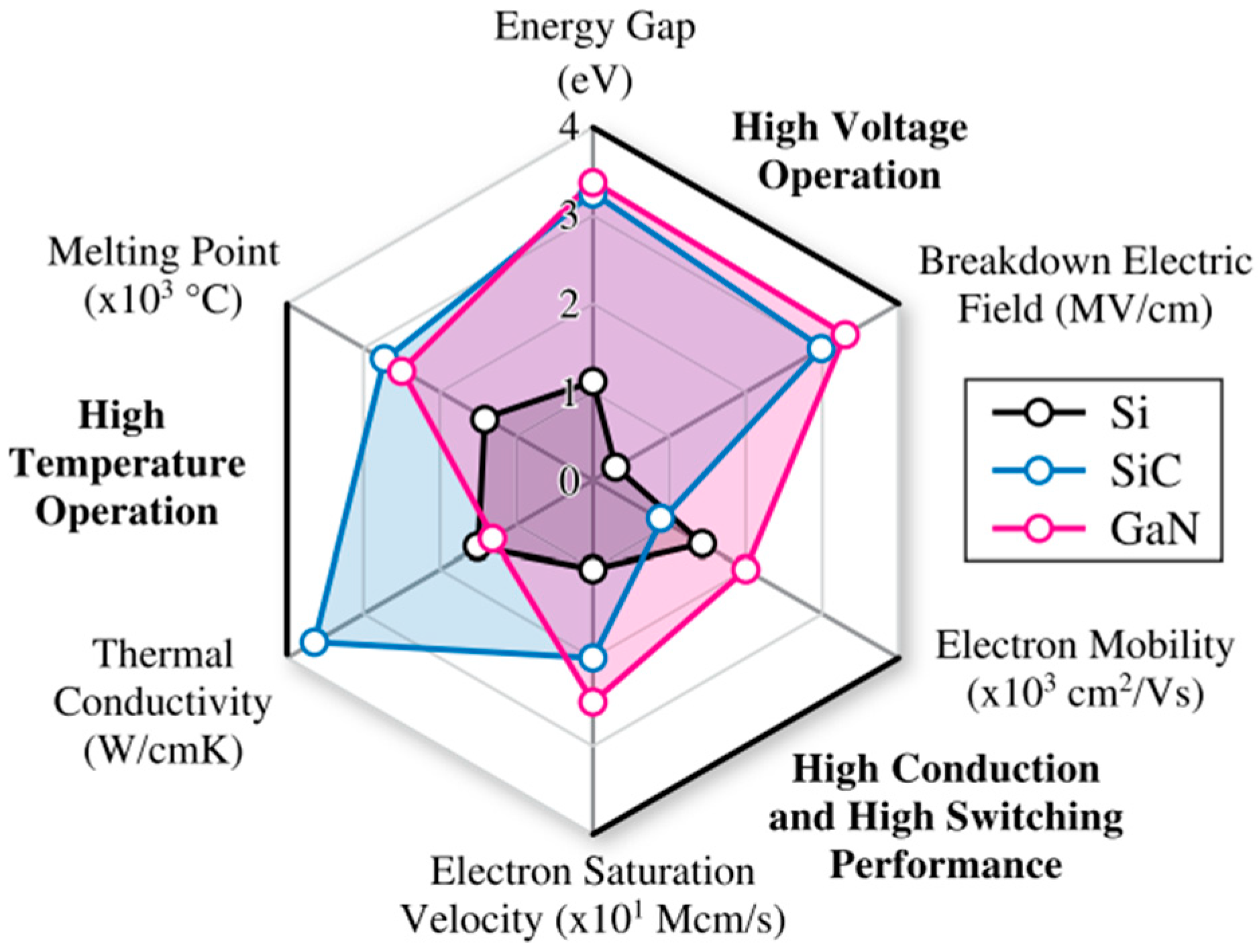
| Symbol | Si | SiC | GaN |
|---|---|---|---|
| Bandgap energy (eV) | 1.12 | 3.26 | 3.45 |
| Melting point (×103 °C) | 1.4 | 2.7 | 2.6 |
| Thermal conductivity (W/m.K) | 1.5 | 4.9 | 1.3 |
| Critical electric field (MV/cm) | 0.3 | 3.2 | 3.5 |
| Electron saturation velocity (107 cm/s) | 1 | 2 | 2.5 |
| Electron mobility (×103 cm2 /Vs) | 1.4 | 0.9 | 1.8 |
| Parameter | Silicon (Si: MOSFET, IGBTS) | Silicon Carbide (SiC: MOSFETs, Schottky Diodes) | Gallium Nitride (GaN: HEMTs) |
|---|---|---|---|
| Switching Speed | Moderate [54,55,56,57,58] | High [66,67,68] | Very high (MHz range) [82,83,84] |
| Voltage range in EVs | Low–Medium (<1200 V) [54,55,56,57,58] | High (≥1700 V, 800 V) [69,70,71] | Medium (<900 V, OBC/DC-DC) [82,83,84,85] |
| Efficiency | Moderate (limited by conduction and switching losses) [56,57,58] | Very high (>98% in traction inverters) [66,67,68] | Very high (>96% in OBCs, DC-DCs) [85,86,87] |
| Thermal Management | Requires bulky cooling [56,57,58] | Better heat dissipation [62,63,64,65] | Easier cooling, but high thermal flux density [88,89,90] |
| Main EV applications | Legacy modules, cost-sensitive systems [48,49,50] | Traction inverters, fast chargers, high-voltage OBCs [66,67,68,69,70,71] | OBC, DC-DC converters, auxiliary modules [85,86,87] |
| Advantages | Mature, low-cost, well-established ecosystem [48,49,50] | High voltage capability, robustness, supports 800 V EVs [66,67,68,69,70,71] | High-frequency switching, compact/lightweight systems [82,83,84,85,86,87] |
| Limitations | High losses at high-voltage/frequency, bulky passive components [52,53,54,55,56,57,58] | High wafer/device cost, limited supply chain [72,73,74,75] | Voltage limited (<900 V), reliability and packaging challenges [95,96,97,98,99,100,101,102] |
| Commercial Adoption | Older EV platforms, low-voltage parts [48,49,50,51,52,53,54,55,56,57,58,59] | Tesla, Lucid, Hyundai, BYD (traction inverters, OBCs) [66,67,68] | Tier-1 suppliers in OBCs, DC-DC (size/weight reduced by 40%) [91,92,93,94] |
| Ref 1 | Year | Vth (V) | BD (V) | Key Results | Main Limitations | EV Relevance |
|---|---|---|---|---|---|---|
| [144] | 2022 | 1.73 | 1205 | Demonstrated p-NiO gate on AlGaN/GaN HEMT, achieving normally off operation with stable Vth and very small Vth shift under stress. High BD voltage >1200 V on Si substrate. | Thermal conductivity of Si substrate inferior to SiC; p-NiO integration still in early research stage; long-term stability not fully validated. | Highly relevant: Shows potential of alternative p-NiO gate designs for >1 kV class HEMTs on Si, offering cost-effective solutions for EV power electronics. |
| [146] | 2021 | 3.9 | 1200 | Introduced a drain-side thin p-GaN structure that reduces peak electric fields and suppresses dynamic RON degradation. Achieved stable high-voltage operation with BV = 1200 V, demonstrating EV suitable robustness. | Fabricated on sapphire substrate, which limits thermal conductivity vs. SiC; long-term stress reliability data limited. | Highly relevant: shows that optimized p-GaN design can combine normally off behavior with >1 kV BD voltage, directly applicable to EV inverters and chargers. |
| [147] | 2023 | 1.5 | 776 | Introduced an active passivation scheme that dynamically screens surface traps, reducing current collapse and dynamic RON. Demonstrated stable switching and improved gate robustness under stress. | The work does not push BD voltage > 1 kV; the study focuses mainly on surface/reliability engineering. | Important for EV since dynamic RON stability and suppression of trapping are critical under high frequency hard switching. |
| [154] | 2024 | 7.1 | 1980 | Demonstrates very high Vth and nearly 2 kV off-state BV in a p-GaN gated device, promising gate robustness and blocking. | Limited public experimental detail in summary; long-term reliability and reproducibility need verification. | Directly relevant: shows p-GaN can be engineered for near 2 kV class blocking when combined with appropriate epi and geometry. |
| [155] | 2024 | 0.9 | 2655 | Introduced super junction charge balance to achieve record high BV and stable dynamic performance | Fabrication complexity; needs precise charge balance control | Highly relevant: BV > 2.5 kV makes it suitable for EV traction inverters and onboard chargers requiring >1200 V devices |
| Ref 1 | Year | Vth (V) | BD (V) | Key Results | Main Limitations | EV Relevance |
|---|---|---|---|---|---|---|
| [156] | 2021 | 1.5 | 1447 | Introduced ZrOx trapping layer in gate stack + partial recess; achieved normally off operation with low RON, reduced gate leakage, and stable threshold. | Threshold stability over long-term stress still under evaluation, potential reliability concerns with ZrOx trapping dynamics under high temperature. | Strong candidate for EV inverters and converters, since it combines low RON and >1.4 kV BV with normally off operation. |
| [157] | 2025 | 2.6 | 830 | Demonstrated that thinner AlGaN barriers improve normally off operation (higher Vth) but reduce 2DEG density, impacting RON. Optimized design achieved a balance between positive Vth, low RON, and reasonable BV. | BD voltages below 1.2 kV limit direct EV traction inverter use; experimental validation limited compared to simulations. | Relevant for EV converters/OBCs where normally off operation + reliability are critical, though BV needs further enhancement for >1200 V class |
| [158] | 2023 | 2 | 1190 | Demonstrated precise recessed gate formation by atomic layer etching (ALE) plus a gate field plate. Achieved high drain current (608 mA/mm), low surface damage, improved threshold control, and BV = 1190 V at 1 mA/mm. | Long-term reliability and performance under hard switching not fully characterized. Process complexity (ALE + field-plate alignment) may affect manufacturability. | Highly relevant, shows a practical recessed gate MIS-HEMT route to reach 1.2 kV class blocking with normally off operation and low RON, pending reliability and large-area manufacturability validation. |
| Ref 1 | Year | Vth (V) | BD (V) | Key Results | Main Limitations | EV Relevance |
|---|---|---|---|---|---|---|
| [160] | 2025 | 2 | 1200 | Introduced polarization super junction (PSJ) concept in GaN, using cascode to achieve normally off operation. Device shows BV = 1200 V, low dynamic RON, and stable switching. Highlights better electric field distribution due to PSJ design. | Cascode introduces parasitics and packaging complexity; BV capped at 1.2 kV, which may not be sufficient for traction inverters (>1.7 kV) | Strong EV relevance for OBC, 400–800 V and DC–DC converters, but less suitable for main drive inverters without scaling to higher BV. |
| [161] | 2019 | 1.2 | 1200 | Achieved 1200 V BV on cascode by combining GaN E-mode control with SiC high-voltage handling. | Hybrid structure; higher parasitics from SiC JFET; integration challenges. | Compatible with EV fast chargers and traction inverters requiring >1 kV operation. |
| [162] | 2025 | 1.3 | 970 | Cascode achieved higher BV than standalone p-GaN HEMT (784 V), improved switching, stable +1.3 V Vth | BV < 1.2 kV, needs optimization for EV traction | Promising for 650–900 V EV applications (onboard chargers, auxiliary systems) |
| Ref 1 | Year | Barrier (Al%) | Key Results | Main Limitations | EV Relevance |
|---|---|---|---|---|---|
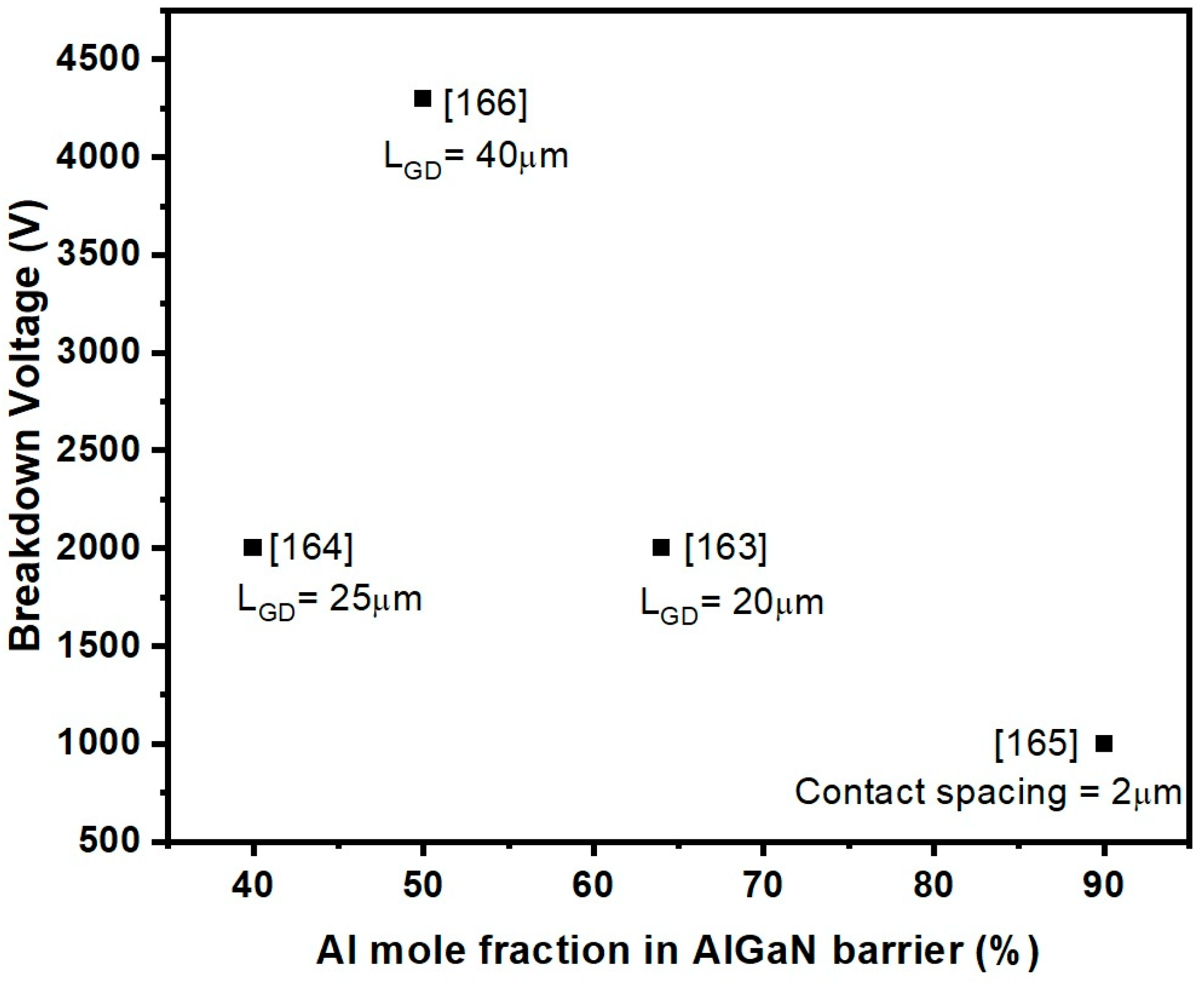
| [163] | 2024 | 64% | BV > 3 kV (pre passivation), 2 kV (post passivation), dynamic RON increase <10%, strong 2DEG confinement | Very high Al → large lattice mismatch, mobility penalty and dislocation risk, requires field-plate and passivation to manage peak E field. | Demonstrates path to kV class GaN for traction/medium voltage power electronics |
| [164] | 2021 | 40% | 2.0 kV reverse blocking reported (device/variant dependent). | Large LGD/field-plate needed for multi kV, trade-offs in area and parasitics for power modules. | Directly relevant—shows 2 kV class blocking on Si substrate (OBC/some inverter roles). |
| [165] | 2019 | 90% | >1000 V at 2 µm spacing | Mobility penalty (µ =340 cm2/V·s) due to high Al% and thin channel, reduced drive current compared to conventional GaN | Demonstrates feasibility of using high Al barrier thin channel structures for >1 kV operation, relevant for high-voltage EV power conversion |
| [166] | 2021 | 50% | Demonstrated record high off-state BV (>4 kV) with leakage < 1 µA/mm, high BD field = 5.5 MV/cm, regrown ohmic contacts improved current injection | Relatively low drain current density (=0.1 A/mm); fabrication complexity due to regrown ohmics, scalability to large wafers not yet proven | Promising for high-voltage EV power converters (OBCs, inverters) where >1200 V class is needed, high Al content offers thermal stability at elevated junction temperatures |
| Ref 1 | Year | SL/Buffer Configuration | 2DEG Density | Mobility | Outcomes |
|---|---|---|---|---|---|
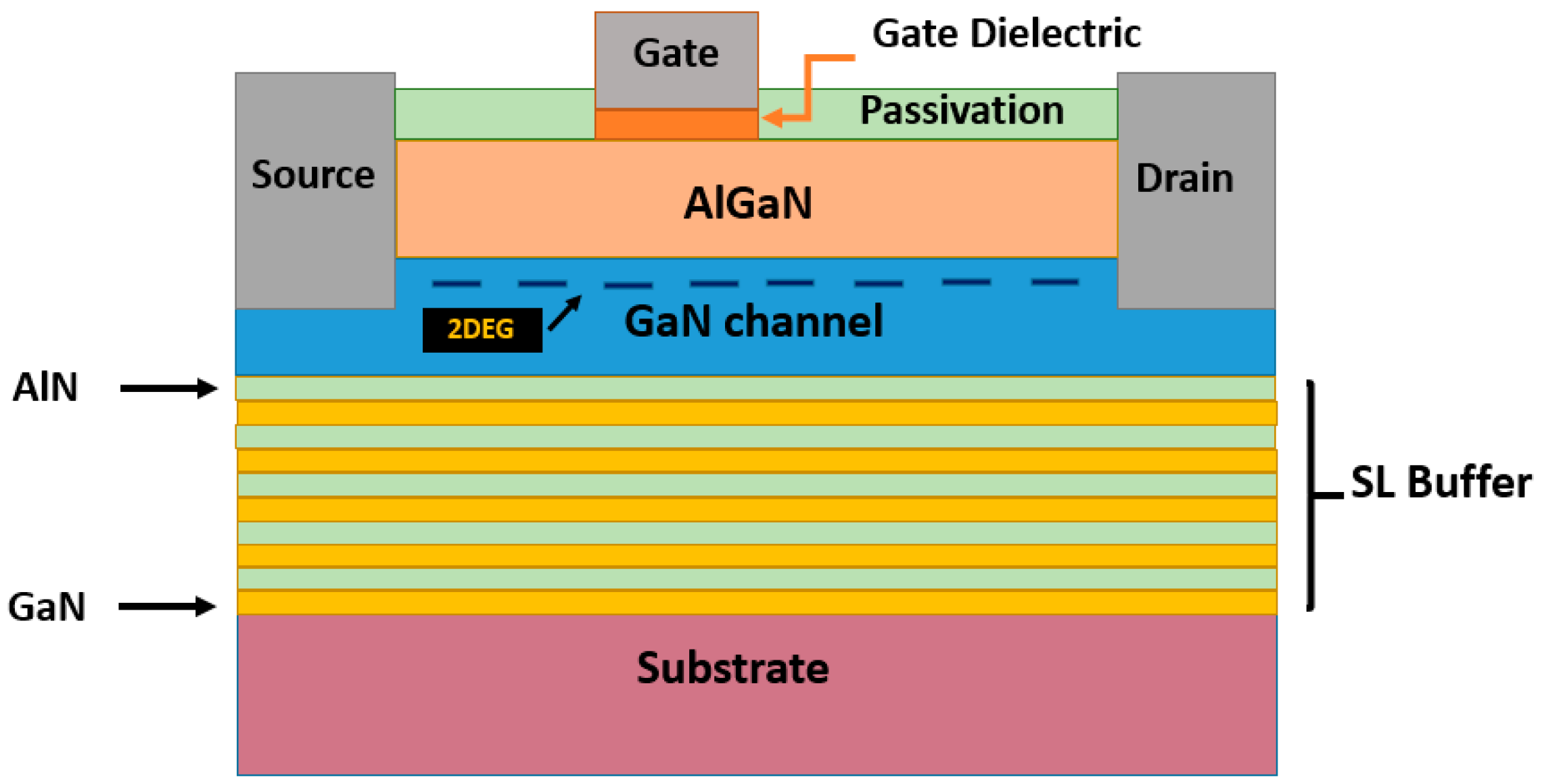
| [167] | 2023 | AlN/GaN SL buffer, 2.2 µm thick | 1.04 × 1013 cm−2 | 1760 cm2/V·s | Improved crystal quality and reduced buffer leakage compared to non-SL buffer, better surface roughness, and BD performance improved. |
| [168] | 2023 | The 1.84 µm thick SL buffer structure features 80 periods of AlN/GaN (2/21 nm) | 8.2 × 1012 cm−2 | 1770 cm2/V·s | BD/leakage and dynamic performance (e.g., trapping during off-state stress) improved, SL buffer thickness/period ratio shown to critically affect leakage and field distribution beneath the buffer and barrier layers. |
| [169] | 2020 | SL-based buffer with 3.8 µm AlN/GaN SL (140 periods) | 1.30 × 1013 cm−2 | 1600 cm2/V·s | Lower trapping, improved temperature behavior and BD voltage, leakage/trapping metrics significantly improved for SL buffer designs. |
| [170] | 2024 | SL-based buffer with 1.15 µm AlN/GaN SL (37 periods) | 1.02 × 1013 cm−2 | 1700 cm2/V·s | BD voltage improved relative to non-SL buffer control, leakage currents lower, contact resistance improved, SL + back barrier combination helps electric field spread and isolation. |
| Ref 1 | Year | Structure | LGD (µm) | BD (V) | Key results | Main limitations | EV Relevance |
|---|---|---|---|---|---|---|---|
| [171] | 2024 | Design Optimization of HBB-HEMT with Neural Networks | 6 | 1640 | Excellent BV vs. Ron trade-off in simulation, field modulation and interface position well explored. | Requires precise epitaxy, simulated, not yet reported experimentally. | Strong candidate for EV switching and traction inverter design, suggests path to >1.6 kV with manageable Ron. |
| [172] | 2024 | Fe-doped back barrier AlGaN/GaN HEMT | 15 | 1700 | Achieved 1700 V BV with effective suppression of buffer leakage and improved field distribution. Fe doping enhanced charge compensation and improved thermal reliability. | Doping process complexity, higher interface states may affect mobility if not optimized. | Directly relevant to EV power converters where BV > 1.2 kV is needed, Fe-doping gives robust trade-off between BV and reliability. |
| [173] | 2023 | AlN/GaN-on-SiC with thin AlGaN back barrier | 10 | 1230 | Thin AlGaN back barrier redistributes vertical electric field, reduces leakage, shifts peak field away from buffer, enabling >1 kV BV while retaining mm-wave frequency capability. | BV limited by short LGD, study optimized mainly for mm-wave performance, not EV-scale high-voltage operation. | Demonstrates back barrier engineering potential. With larger LGD + field plates, similar approaches could scale BV into the 1–3 kV EV range. |
| Substrate | Ref | Year | BD (kV) | Thermal Conductivity (W/m·K) | Dynamic RON | Substrate Cost/Scalability | Industry Status | EV Relevance (OBC/Traction Inverter/DC-DC) |
|---|---|---|---|---|---|---|---|---|
| Si | [174] | 2022 | >1.2 | 150 | Low buffer trapping → stable RON under high VDS | Low-cost, large wafer (200 mm) → scalable | Pre-commercial/Pilot lines | Suitable for OBCs and DC/DC converters in EVs due to 1.2 kV capability |
| [175] | 2025 | - | ||||||
| SiC | [173] | 2023 | 1.5–2.0 | 400 | Back barrier design reduces leakage, improves VBR stability | More expensive, wafer size limited (≤150 mm) | Mature R&D, some commercial | Relevant for traction inverters and high-power OBCs, where high VBR and thermal stability are required |
| [176] | 2021 | 1.2 | ||||||
| Diamond | [177] | 2024 | >1.5 | 1800– 2000 | Reduced self-heating → lower RON degradation under stress | Very high cost, scalability limited | Early-stage R&D | Long-term traction inverter candidate due to extreme thermal management, but not yet manufacturable at scale |
| [178] | 2025 | - | ||||||
| QST | [179] | 2024 | 1.5 | 500 | Stable dynamic RON due to low stress/warpage | Moderate cost, scalable to 200 mm | Emerging/Pilot Production | Promising for 650–1200 V EV applications (OBC, DC/DC, traction) |
| [180] | 2022 | 1.2 | ||||||
| GaN | [181] | 2025 | 150 | 130 | Increased effective dynamic Ron | High Cost | Emerging/Pilot Production | OBC/DC-DC (near-term research use) |
| [182] | 2025 | 755 |
| Architecture | Key Structural Feature | Main Advantages | Key Limitations | EV Power Electronics Relevance |
|---|---|---|---|---|
| Depletion-Mode GaN HEMT | Standard Heterostructure | High mobility simple structure | Safety concerns, complex gate drives | Limited (research, cascode use) |
| p-GaN Gate GaN HEMT | p-GaN cap under gate | Enhancement mode | Gate reliability, Threshold instability | OBC, DC to DC converters |
| Gate Recess GaN HEMT | Etched AlGaN under gate | Low gate leakage, Fast switching | Process control sensitivity | Medium-voltage EV sub system |
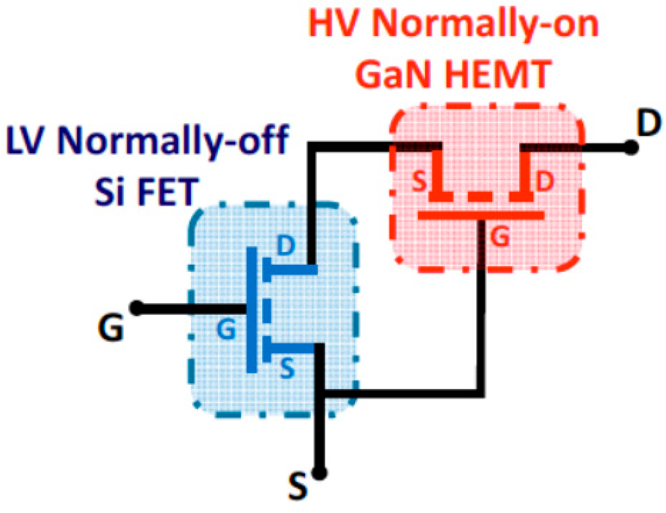
| Cascode GaN HEMT | Depletion-mode GaN HEMT + Si MOSFET | Easy drive compatibility | Added parasitics, lower speed | Early EV adoption |
| High Al AlGaN Barrier | Increased Al mole fraction | Higher 2DEG density | Increased strain, Reliability issues | High-voltage operation |
| Superlattice Buffer | Multi-layer strain Management | Reduced leakage, better breakdown | Growth complexity | High-voltage EV inverters |
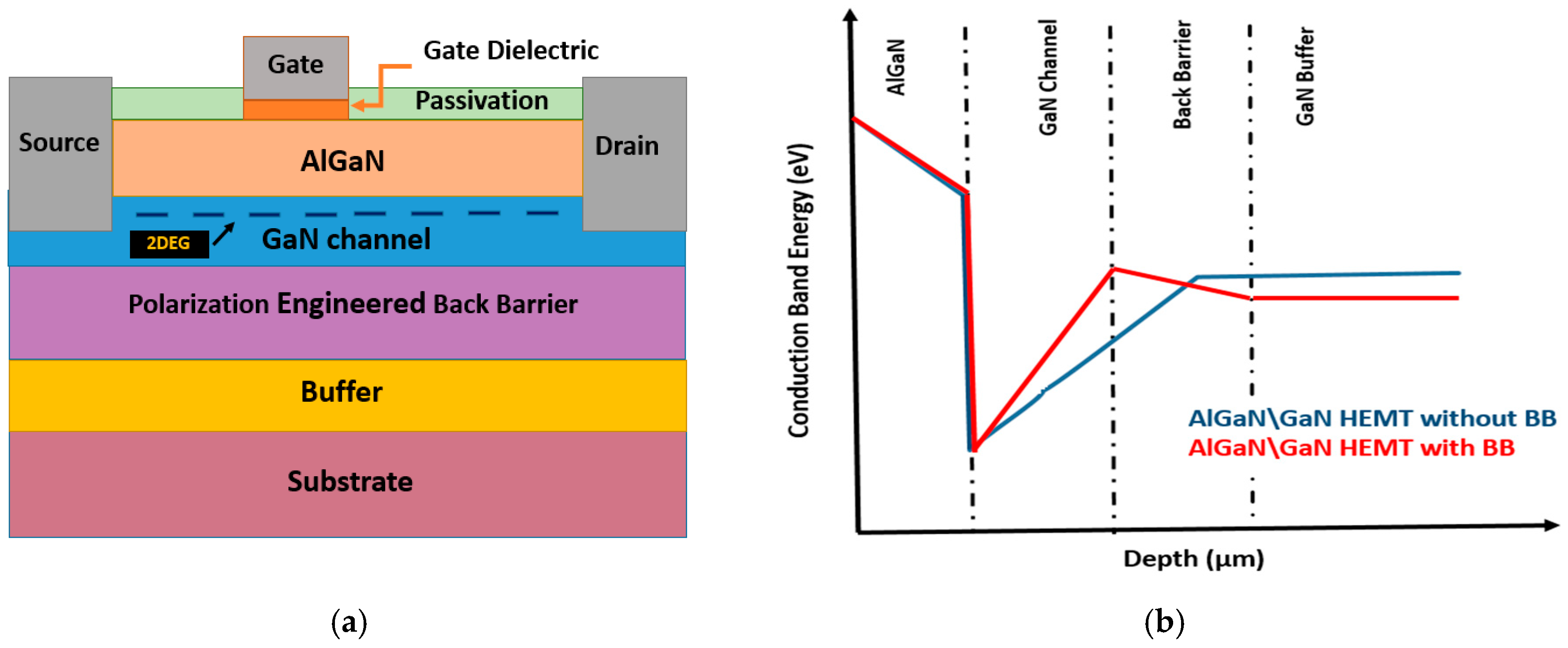
| Polarization Back Barrier | Engineered Polarization Layer | Reduced current collapse | Added epitaxial complexity | High-reliability EV system |
| GaN-on-Si | Si Substrate | Low cost, large wafers | Thermal and breakdown limits | Cost-sensitive EV electronics |
| GaN-on-SiC | SiC substrate | Excellent thermal performance | High cost | Traction Inverters |
| GaN-on-Diamond | Diamond Heat spreader | Ultra-high thermal conductivity | Immature very costly | Future high-power-density EVs |
| GaN-on-QST | Engineered composite substrate | Reduced stress improved yield | Limited maturity | Emerging EV platform |
| GaN-on-GaN | Native GaN substrate | Lowest defect density | Extremely expensive | Research, premium EV technology |
| Vendor | VDS (V) | IDS (A) | RDS (ON) mΩ | Power Dissipation (W) |
|---|---|---|---|---|
| TP65H015G5WS (Renesas/Transphorm Gen-V) | 650 | 93 | 15–18 | 266 |
| GS66516T (GaN Systems) | 650 | 60 | 25 | 450 |
| GS66508T (GaN Systems) | 650 | 30 | 50 | 250 |
| TP65H035G4WS (Renesas/Transphorm Gen-IV) | 650 | 46 | 35 | 119 |
| TP65H050G4WS (Transphorm Gen-IV) | 650 | 30 | 50 | 119 |
| IGLT65R035D2 (Infineon CoolGaN G5) | 650 | 47 | 35 | 154 |
| IGLD65R110D2 (Infineon CoolGaN G5) | 650 | 14 | 110 | 51 |
| CG65050TAD/CG65050DAD (CloudSemi) | 650 | 40 | 39 | 236 |
| Ref | Vendor/ Platform | Device Family | Qualification Status | Max TJ (°C) | Reliability Information | Automotive Adoption Status |
|---|---|---|---|---|---|---|
| [183] | Infineon | CoolGaN™ G5 | JEDEC qualified; AEC-Q101 targeted | 175 | HTOL, HTRB, power cycling reported | Automotive programs ongoing |
| [184] | Transphorm | Gen-IV/Gen-V | JEDEC qualified; automotive-grade variants available | 175 | Long-term reliability and field data reported | Used in automotive OBCs |
| [185] | GaN Systems | GS-650 V series | JEDEC qualified; not AEC-Q101 | 150–175 | Accelerated lifetime testing reported | Evaluation/pilot adoption |
| Ref 1 | Device | Stress\Conditions | Metrics Reported |
|---|---|---|---|
| [193] | TP65H035WS (Group D1) 2 650 V cascode GaN HEMT | H3TRB test (humidity + high-temp + high-voltage reverse bias) 85 °C, 85% RH (relative humidity), VDS = 520 V, Duration: 1000 h | Average leakage current during H3TRB: 10–20 µA |
| [194] | 1200 V lateral p-GaN HEMTs on 9 μm GaN | HTRB (high-temperature reverse bias), 1200 V reverse-bias, high-temperature, 1000 h | Drain leakage: < 10 µA, Vth shift: negligible. RON: no measurable change. Breakdown voltage: remains 1.8 kV. |
| [195] | AlGaN/GaN HEMT with dual-layer surface structure | Pulsed test: VG = −6 V, VDS = 20 V (pulsed) | Reported negligible current collapse ≈ 3% under the stated pulsed conditions |
| [196] | p-GaN gate AlGaN/GaN on Si | Off-state drain stress | Vth drift up to 40% under off state drain bias |
Disclaimer/Publisher’s Note: The statements, opinions and data contained in all publications are solely those of the individual author(s) and contributor(s) and not of MDPI and/or the editor(s). MDPI and/or the editor(s) disclaim responsibility for any injury to people or property resulting from any ideas, methods, instructions or products referred to in the content. |
© 2026 by the authors. Licensee MDPI, Basel, Switzerland. This article is an open access article distributed under the terms and conditions of the Creative Commons Attribution (CC BY) license.
Share and Cite
Hamza, H.; Rusli, J.R.; Jarndal, A. GaN HEMTs for Electric Vehicle Power Electronics: Device Architectures, Reliability and Next-Generation Wide Bandgap Opportunities. Energies 2026, 19, 1752. https://doi.org/10.3390/en19071752
Hamza H, Rusli JR, Jarndal A. GaN HEMTs for Electric Vehicle Power Electronics: Device Architectures, Reliability and Next-Generation Wide Bandgap Opportunities. Energies. 2026; 19(7):1752. https://doi.org/10.3390/en19071752
Chicago/Turabian StyleHamza, Husna, Julie Roslita Rusli, and Anwar Jarndal. 2026. "GaN HEMTs for Electric Vehicle Power Electronics: Device Architectures, Reliability and Next-Generation Wide Bandgap Opportunities" Energies 19, no. 7: 1752. https://doi.org/10.3390/en19071752
APA StyleHamza, H., Rusli, J. R., & Jarndal, A. (2026). GaN HEMTs for Electric Vehicle Power Electronics: Device Architectures, Reliability and Next-Generation Wide Bandgap Opportunities. Energies, 19(7), 1752. https://doi.org/10.3390/en19071752