Article

Internal Power Loss Modeling and Efficiency Evaluation of Full-Bridge DC–DC Converters Based on Load-Current-Dependent Loss Coefficients

1
Department of Electrical & Control Engineering, Cheongju University, Cheongju 28503, Republic of Korea
2
R&D Division, Taekang Inc., Yongin 17015, Republic of Korea
*
Author to whom correspondence should be addressed.
Energies 2026, 19(4), 899; https://doi.org/10.3390/en19040899
Submission received: 19 January 2026 / Revised: 4 February 2026 / Accepted: 6 February 2026 / Published: 9 February 2026
(This article belongs to the Section F: Electrical Engineering)

Abstract

In this paper, a theoretical methodology is proposed for the systematic analysis of the power conversion efficiency of a full-bridge converter. Using the steady-state analysis results derived from the equivalent circuit, we introduced the concept of “loss coefficients” by categorizing parameters based on their correlation with load power and current. In particular, the loss factors for key components were organized in a tabular format according to their respective contributions to the load current. Furthermore, this study presented the contribution of the rectifier’s internal loss and overall power conversion efficiency through graphical representations to facilitate intuitive understanding. Finally, to verify the validity of the efficiency analysis incorporating the proposed loss factors, a loss and efficiency analysis was conducted on a 300 W-class full-bridge converter, and the results were compared with measured data from an experimental prototype. The results demonstrate that, at maximum load power, the discrepancy between the experimental and theoretical power conversion efficiency values ranged from a maximum of 1%. Consequently, it was confirmed that the proposed analysis method based on effective currents of key components and loss coefficients reflecting internal parasitic elements provides a valid approach for characterizing internal power loss and conversion efficiency relative to load current.

1. Introduction

In the contemporary landscape of power electronics, the demand for high-performance and high-efficiency power conversion devices has reached an unprecedented level. As global industries undergo a rapid transition toward electrification and digitalization, the role of DC–DC converters has expanded from simple voltage regulation to becoming the critical backbone of complex energy ecosystems. From electric vehicles (EVs) and renewable energy systems to hyperscale data centers, telecommunication base stations, and sophisticated industrial automation, the efficient management of electrical energy is now a primary determinant of system reliability, operational cost, and environmental sustainability [1,2,3].
Among these diverse applications, the modern transportation sector, particularly the electric vehicle (EV) industry, stands as a prime example of where power conversion efficiency is paramount. In an EV, the efficiency of on-board DC–DC converters is not merely a technical specification; it is a critical factor that directly influences the vehicle’s driving range, thermal management requirements, and battery longevity. As charging infrastructures move toward ultra-fast charging capabilities and battery management systems (BMS) require higher precision, there is an intensifying push to achieve extreme miniaturization and weight reduction. These requirements act as major design drivers, accelerating technological advancements in high-power-density converters that can operate reliably under stringent low-profile and high-temperature conditions.
In response to these rigorous demands, the industry has seen a paradigm shift toward Wide Bandgap (WBG) semiconductors and advanced switching topologies. Leading power semiconductor companies, such as Texas Instruments (TI), have demonstrated the potential of these technologies by achieving peak efficiencies exceeding 99.5% in specialized switching power supplies. Such high-water marks in efficiency highlight that the traditional margins for design error have vanished. Achieving these performance levels requires not only superior components but also a profound understanding of every internal loss mechanism within the converter.
Despite the critical need for precision, conventional loss modeling approaches for DC–DC converters often present a trade-off between accuracy and practical utility. Classical physics-based models provide deep insights into individual component behavior—such as the nonlinear switching characteristics of MOSFETs or the complex core loss mechanisms in magnetic materials—but they are frequently too computationally intensive or specific to be applied effectively during the initial system-level design phase. Conversely, simplified behavioral models often fail to account for the impact of parasitic elements and variable load conditions, leading to significant discrepancies between theoretical predictions and real-world prototype performance. Relying on complex iterative simulations can hinder the rapid optimization process necessary for fast-paced product development cycles [4,5,6].
This study aims to bridge this gap by proposing a systematic theoretical methodology for analyzing the power conversion efficiency of a full-bridge DC–DC converter, which remains one of the most widely utilized and versatile topologies for high-power on-board applications. The core contribution of this paper is the introduction of a unified analytical framework based on the concept of “Loss Coefficients.” By conducting a rigorous steady-state analysis of the equivalent circuit, we categorize the myriad internal power loss factors—ranging from conduction and switching losses to parasitic resistance and core losses—into three distinct coefficients based on their mathematical correlation with the load current. This coefficient-based approach provides several significant advantages. First, it simplifies the complex interactions of parasitic elements into a manageable set of parameters, allowing designers to intuitively visualize and predict the efficiency curve across the entire load spectrum. Second, it identifies the dominant loss factors at specific operating points, enabling targeted optimization to improve either light-load or full-load performance. Third, the proposed framework is highly adaptable to modern high-performance components. In this research, we incorporate the characteristics of cutting-edge devices, such as Infineon’s MOSFETs with ultra-low on-resistance and Tokyo Denki Kagaku’s (TDK’s) advanced high-frequency magnetic materials, ensuring the model’s relevance to current industrial standards.
The structure of this paper is organized as follows. Section 2 provides a detailed steady-state analysis of the full-bridge converter and defines the equivalent circuit including all relevant parasitic components. Section 3 derives the systematic methodology for extracting the loss coefficients and establishes the theoretical efficiency equations. Section 4 presents a comprehensive loss analysis and explores the sensitivity of the system to various design parameters. In Section 5, the validity of the proposed model is rigorously tested against experimental data obtained from a 150 W-class prototype circuit. The comparison includes performance metrics across a wide load range, from 10% (light-load) to 100% (rated-load) conditions, to verify the scientific accuracy and tolerance limits of the theoretical model. Finally, Section 6 concludes the paper by discussing the potential for extending this methodology to other isolated DC–DC topologies and identifying future research directions. Through this integrated approach, this study contributes to the ongoing efforts toward the miniaturization and optimization of next-generation power conversion systems for aerospace, defense, and EV applications.

2. Steady-State Characteristics of a Full-Bridge Converter

2.1. Basic Circuit of a Full-Bridge Converter

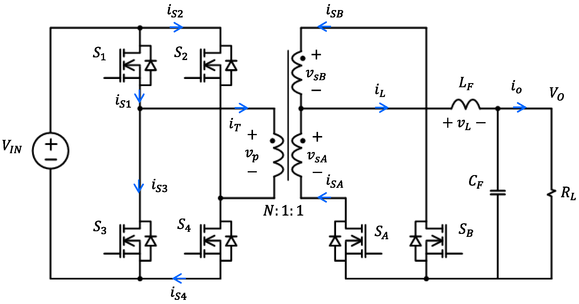
Figure 1 illustrates the fundamental circuit configuration of the full-bridge converter [7,8,9,10]. The diagram depicts the DC input voltage, a center-tapped transformer, four switches on the primary side, synchronous rectifier (SR) switches on the secondary side, an output filter consisting of an inductor and capacitor, and the load resistance. In general, the full-bridge converter allows the entire input voltage to be applied across the primary winding of the high-frequency transformer by utilizing four switching devices. This structural characteristic provides significantly higher power conversion capability compared to other topologies, such as half-bridge or flyback converters. Furthermore, through high-speed switching operations, the transformer flux is utilized symmetrically and balanced in both forward and reverse directions, inherently preventing magnetic core saturation. This feature is well-known for maximizing transformer efficiency and facilitating miniaturization, which is advantageous for high-power-density system designs [11,12,13,14,15].
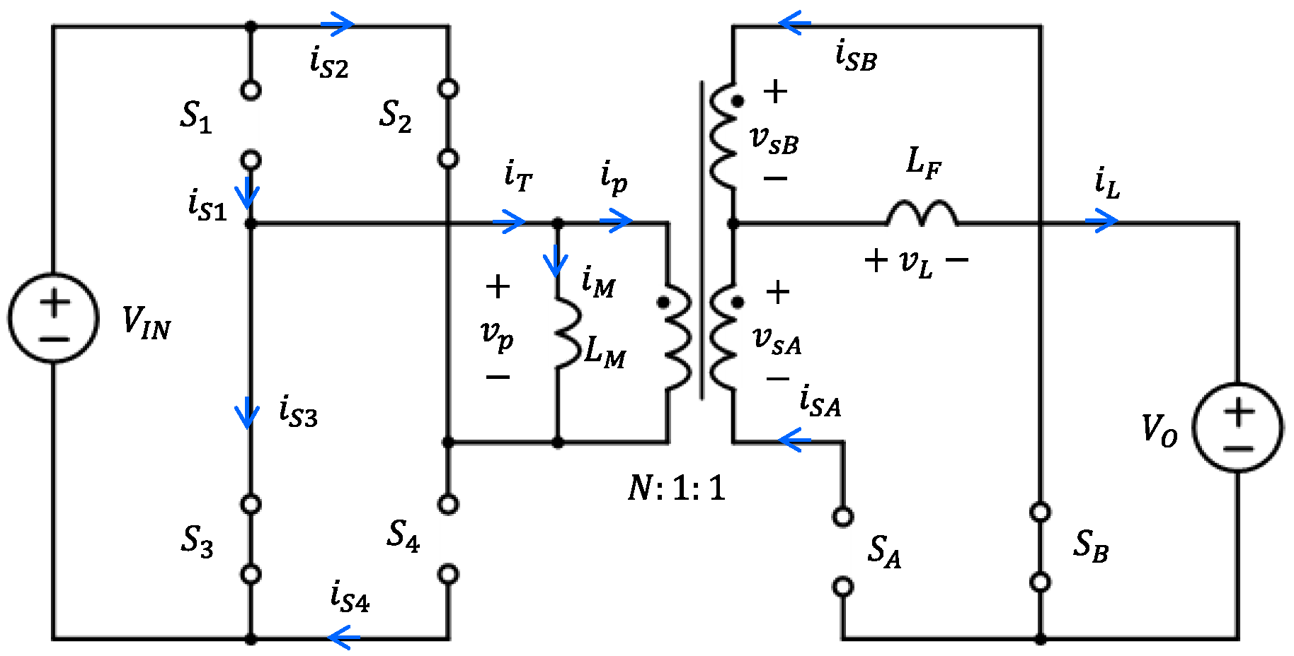
Figure 2 shows the equivalent circuit of the full-bridge converter. In this representation, the transformer is modeled with its primary side magnetizing inductance L M in parallel with an ideal center-tapped transformer. Typically, since the transformer in a full-bridge converter lacks an internal air gap in the magnetic core, it exhibits a large magnetizing inductance L M . This characteristic complicates flux density saturation and ensures stable transformer operation. Additionally, the main switching devices S 1 4 are modeled as ideal switches. Assuming that the cutoff frequency of the output LC filter is significantly lower than the switching frequency, the output capacitor C F can be treated as a constant voltage source V o under steady-state conditions. Here, the ideal switch is characterized by zero conduction resistance in the ON state and infinite impedance in the OFF state. In the figure, the arrows indicate the direction of the current, and the black dots indicate the winding direction of the transformer. The arrows indicate the direction of the current, and the black dots indicate the winding direction of the transformer. For the analysis, gate drive losses and losses associated with parasitic components are neglected. Furthermore, the internal resistances of the transformer and inductor, as well as the core losses, are assumed to be zero [16,17,18,19,20,21].

2.2. Steady-State Analysis

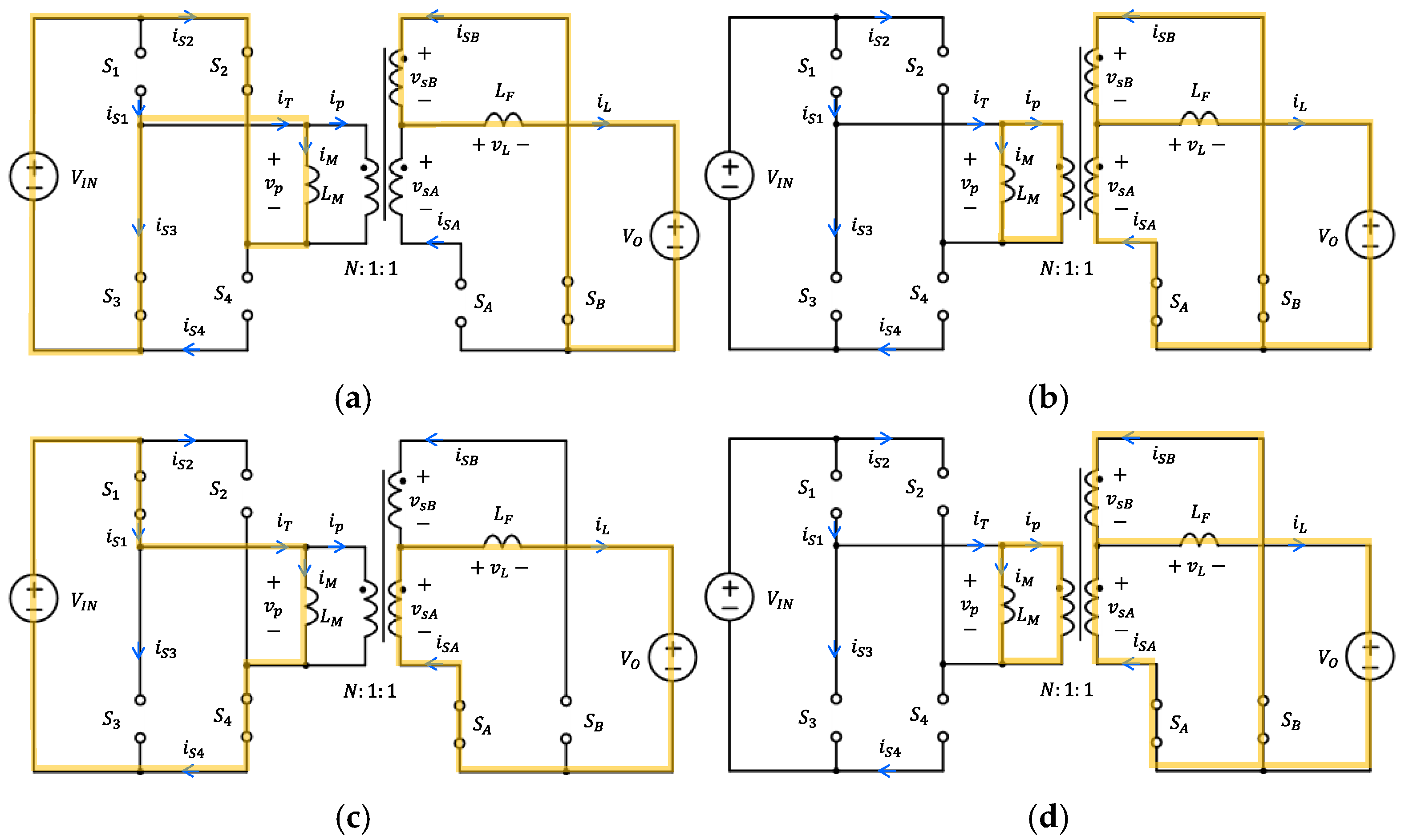
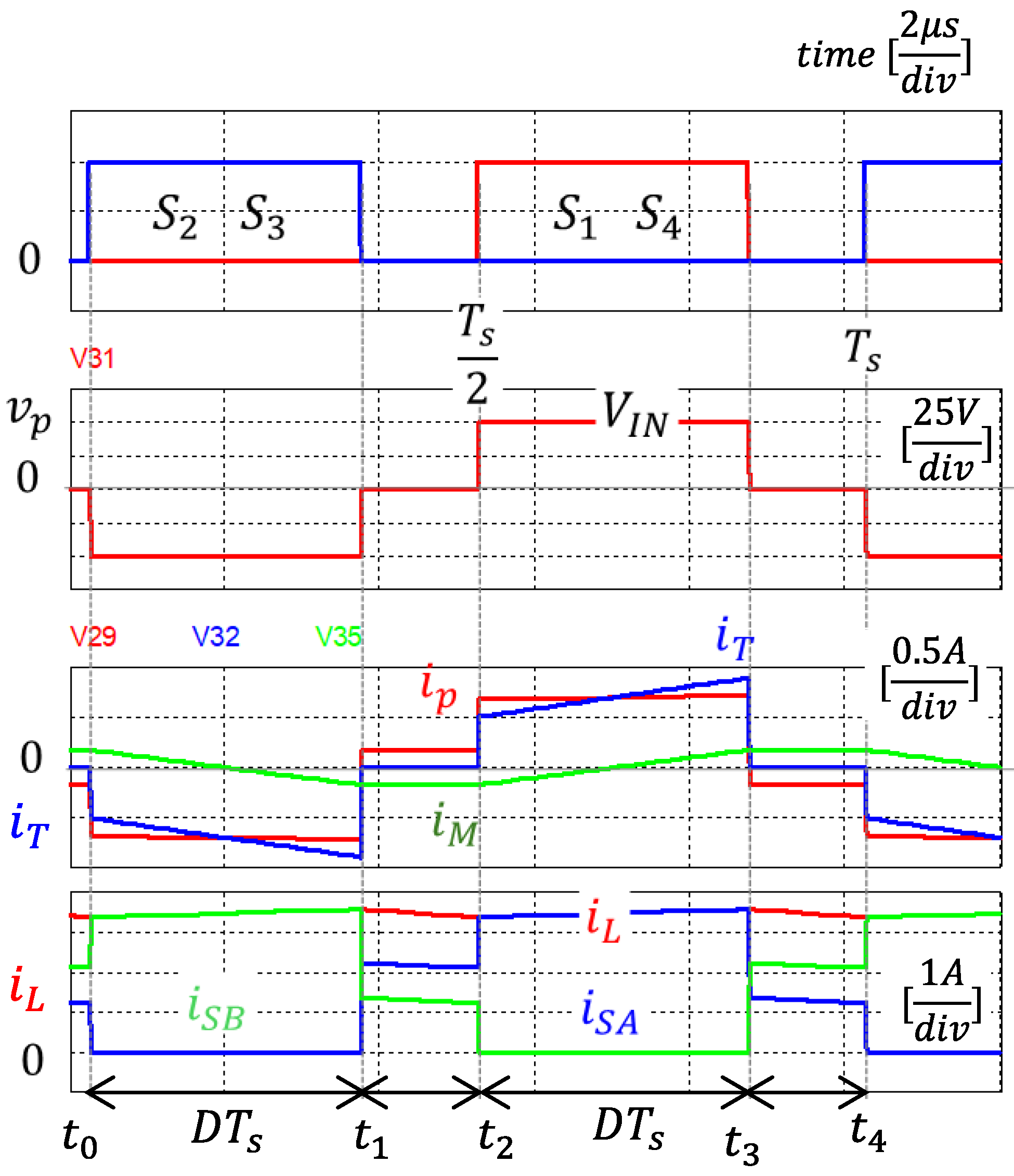
Since the full-bridge converter configures a total of four switches S 1 , 2,3 , 4 on the primary side in a bridge topology, a short-circuit condition occurs if two switches in the same leg (upper and lower) are turned on simultaneously. Therefore, power is transferred from the input to the output only when the diagonally positioned switches are turned on at the same time. Due to the presence of the transformer’s magnetizing inductance L M , a specific period is required to reset the magnetizing current i M ; during this interval, all four switches remain in the OFF state. Consequently, under a constant switching frequency, the operation within a single switching cycle can be characterized by four distinct operating modes. Figure 3 illustrates the equivalent circuits for each operating state when the full-bridge converter shown in Figure 2 operates under steady-state conditions. In the figure, the yellow line represents the circulating current. The blue arrow in the picture indicates the direction of the current. Furthermore, Figure 4 presents the steady-state operational waveforms of the key components. Blue line indicates the operating status of switches S 2 , 3 , and red line indicates the operating status of switches S 1 , 4 . From top to bottom, the waveforms in Figure 4 represent the gate driving voltages, the primary-side voltage of the transformer v p , the primary-side current i p , the synchronous rectifier currents i A , B , and the output inductor current i L [22,23,24,25,26,27].
In Figure 3, it is assumed that the four switches S 1 , 2,3 , 4 operate in pairs S 1 , 4 and S 2 , 3 at a constant frequency and a fixed duty cycle. The description for Mode 1 is as follows. As shown in Figure 3a, at time t 0 , switches S 2 and S 3 are turned on, while S 1 and S 4 are turned off. A negative input voltage is applied across the transformer’s primary-side magnetizing inductance L M , as expressed in (1). The output inductor voltage v L and current i L are derived according to the transformer turns ratio N , as shown in (3) and (4), respectively. The magnetizing current i M decreases linearly, with its maximum and minimum values defined by (5) and (6). Mode 1 concludes at time t 1 .
v p = V I N
v L = v s B V o = V I N N V o
N i L = D L F f s V I N N V o = V o 1 2 D 2 L F f s
I M   m a x = i M 2 = N V o 4 L M f s
I M   m i n = i M 2 = N V o 4 L M f s
The description for Mode 2 is as follows. As illustrated in Figure 3b, at time t 1 , all switches— S 1 , S 2 , S 3 , and S 4 —are turned off. During this interval, the magnetizing inductor current i M remains constant, maintaining the same minimum value as defined in (6). The variation in the output inductor current i L is expressed in (9). Due to the voltage at the transformer secondary side, both synchronous rectifier switches, S A and S B , conduct simultaneously. The respective currents i s A , B flowing through these two synchronous switching devices are given by (10) and (11). Mode 2 concludes at time t 2 .
i p = i M = N V o 4 L M f s
i s A + i s B = i L
i T = i M + i p = 0
i L = V o D L F f s
i s A = 1 2 i L + N i p = 1 2 i L N i M
i s B = 1 2 i L N i p = 1 2 i L + N i M
The description for Mode 3 is as follows. The equivalent circuit and operational waveforms for Mode 3 are illustrated in Figure 3c and Figure 4, respectively. In Mode 3, switches S 1 and S 4 are turned on at time t 2 , while S 2 and S 3 are turned off. The input voltage is applied across the transformer’s magnetizing inductance L M , and the magnetizing current i M is defined by (12). The current variation i L and voltage v L of the output inductor are given by (13) and (14), respectively. Furthermore, the primary-side current i T of the transformer is expressed as shown in (15). Mode 3 concludes at time t 3 .
i M = D V I N L M f s = N V o 2 L M f s
i L = D L F f s V I N N V o = V o 1 2 D 2 L F f s
v L = v s V o = V I N N V o
i T = i M + i s A N = i M + i L N
The description for Mode 4 is as follows. The equivalent circuit and operational waveforms for Mode 4 are presented in Figure 3d and Figure 4, respectively. In Mode 4, all four switches S 1 , S 2 , S 3 and S 4 are turned off at time t 3 . The voltage across the transformer’s magnetizing inductance becomes zero, and the minimum values at this time are defined by (16) and (17). Due to the transformer’s secondary-side voltage, both synchronous rectifier switches, S 1 and S B , conduct simultaneously. The currents i s A , B flowing through these two synchronous switching devices are expressed in (18) and (19). Mode 4 concludes at time t 4 .
I M   m i n = D V I N 2 L M f s = N V o 4 L M f s
i p = i M = N V o 4 L M f s
i s A = 1 2 i L + N i p = 1 2 i L N i M
i s B = 1 2 i L N i p = 1 2 i L + N i M
Meanwhile, assuming that the average value of the inductor current is equal to the load current, the current flowing through the synchronous rectifiers can be simplified as shown in the following equation.

I s A 1 2 I o + N 2 V o 4 L M f s   I s B 1 2 I o N 2 V o 4 L M f s
I s A 1 2 I o N 2 V o 4 L M f s   I s B 1 2 I o + N 2 V o 4 L M f s

3. Power Loss of Major Components Linked to Load Current

3.1. Current Effective Value of Main Components

In this paper, to analyze the internal losses and power conversion efficiency of the full-bridge converter, we propose a unified and simplified analytical framework that builds upon existing methodologies. This approach is intended to facilitate efficient converter design during the initial stage. First, the power loss model within the full-bridge converter circuit is defined herein as the “Power Loss Coefficient.” This coefficient serves as a collective term for all factors contributing to internal power dissipation and is expressed as a proportionality constantly relative to power consumption. For this analysis, internal power losses are categorized into four types: conduction loss, switching loss, magnetic loss, and auxiliary power loss.
Generally, conduction losses occurring when current flows through semiconductor or passive components depend on the internal resistance of these devices. Meanwhile, switching losses, which occur during the transition between ON and OFF states, are independent of the load current but depend on parasitic capacitance and switching frequency. Since switching losses increase significantly at high operating frequencies, careful selection of the switching frequency is required. In particular, among the major components used in switching rectifiers, the inductor accounts for both magnetic flux losses which are size- and frequency-dependent and resistive losses caused by internal resistance. In general, internal power loss leads to heat dissipation and acts as a primary factor that degrades the overall efficiency of the power supply system. Table 1 summarizes the characteristic equations for key components derived through the steady-state analysis of the full-bridge converter in the preceding section. This table provides the essential formulas for converter design along with the root mean square (RMS) current values for major components. Notably, the RMS currents are expressed in terms of the load current, demonstrating a proportional relationship between the load current and the RMS values.

3.2. Efficiency and Loss Factor Linked to Load Current

As indicated in Table 1, the RMS current values of the key components can be categorized into those proportional to the load current and those independent of it. Consequently, the internal power loss of the converter can be generalized as shown in (22). In this equation, the power loss is expressed as a quadratic function of the load current, where each term includes a corresponding proportionality constant. Specifically, in (22), the losses independent of the load current are denoted by the I o 0 term, while the losses proportional to the load current and the square of the load current are represented by the I o 1 and I o 2 terms, respectively. In this paper, the coefficients for these power losses, organized by their dependence on the load current, are defined as K 0 , K 1 , and K 2 , which are collectively referred to as the “Loss Coefficients”. The loss coefficient K represents the power loss factor of the components related to the load current; it is determined once the circuit topology is established and is characterized by the specific parameters of the circuit elements. Furthermore, since the internal power loss of the converter is the difference between the input and output power, the power conversion efficiency can be expressed as shown in (23). As evident from the equation, the power loss is not fundamentally caused by the load current itself but rather depends on the loss coefficients K . To improve efficiency, it is crucial to minimize these loss coefficients, particularly noting that K 2 has the most significant impact on the overall loss.
P L = K 0 × I o 0 + K 1 × I o 1 + K 2 × I o 2
E = P o P o + P L × 100
Table 2 summarizes the internal power losses associated with the coefficient K 0 . As indicated in (22), the loss coefficient K 0 is independent of the load current. These include, from top to bottom, the switching losses due to the parasitic capacitance of the primary switches, the switching losses of the synchronous rectifiers, the transformer core loss, the inductor core loss, and the conduction loss of the output capacitor. Table 3 presents the internal power losses related to the coefficient K 2 . The K 1 term, which accounts for losses linearly proportional to the load current, is primarily associated with the constant forward voltage drop of semiconductor diodes. In this study, the adoption of Synchronous Rectifiers (SR) with low on-resistance significantly mitigates such linear losses. Consequently, the internal loss is predominantly governed by the constant switching/core losses K 0 and the quadratic conduction losses K 2 , rendering the impact of the K 1 term negligible under the given operating conditions. The K 2 -related losses, listed from top to bottom, consist of the conduction losses of the primary switches, the conduction losses of the synchronous rectifier switches, the primary and secondary winding losses of the transformer, and the conduction loss of the output inductor. As described above, the transformer and inductor losses are categorized into magnetic core losses and resistive conduction losses from the windings. Regarding the capacitor, the conduction loss is attributed to its internal equivalent resistance. In this case, the loss is independent of the load current and depends instead on the input voltage. This characteristic arises because the DC component of the current is blocked by the capacitor, while only the AC ripple current passes through.

4. Design and Construction of an Experimental Full-Bridge Converter

4.1. Design of an Experimental Full-Bridge Converter

In this paper, to verify the validity of the internal power loss and power conversion efficiency analysis based on the loss coefficients, a 300 W full-bridge converter prototype was constructed, and the experimental results are compared. First, Table 4 presents the electrical specifications of the experimental circuit. The input voltage was set to 36–75 V, which is the standard input range for telecommunication power supplies. The output voltage V o is 5 V, with a maximum output current I o   m a x of 60 A and a total rated power of 300 W. The switching frequency is 240 kHz. The values of the key components can be determined using the steady-state characteristic equations provided in Table 1. The transformer turns ratio N , as shown in (24), was set to 6:1 for the transformer fabrication. The transformer’s magnetizing inductance L M can be calculated using (25), and the values for the output capacitor C F and output inductor L F are determined as expressed in (27) and (28), respectively.
N = 2 D   V I N V o = 6.3
L M 9 N 2 L F V o 4 L F f s I o   m a x + V o 1 2 D m i n = 260   μ H
D m i n = N   V o 2 V I N   m a x = 0.42
C o V o 1 2 D m i n 32 f s 2 L F V c p p = 40   μ F
L F V o 1 2 D m i n 4 f s I o   m i n = 1.5   μ H

4.2. Configuration of an Experimental Full-Bridge Converter

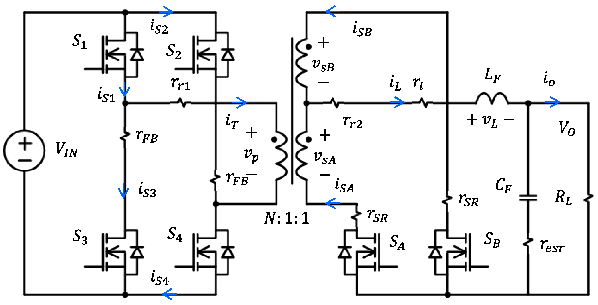
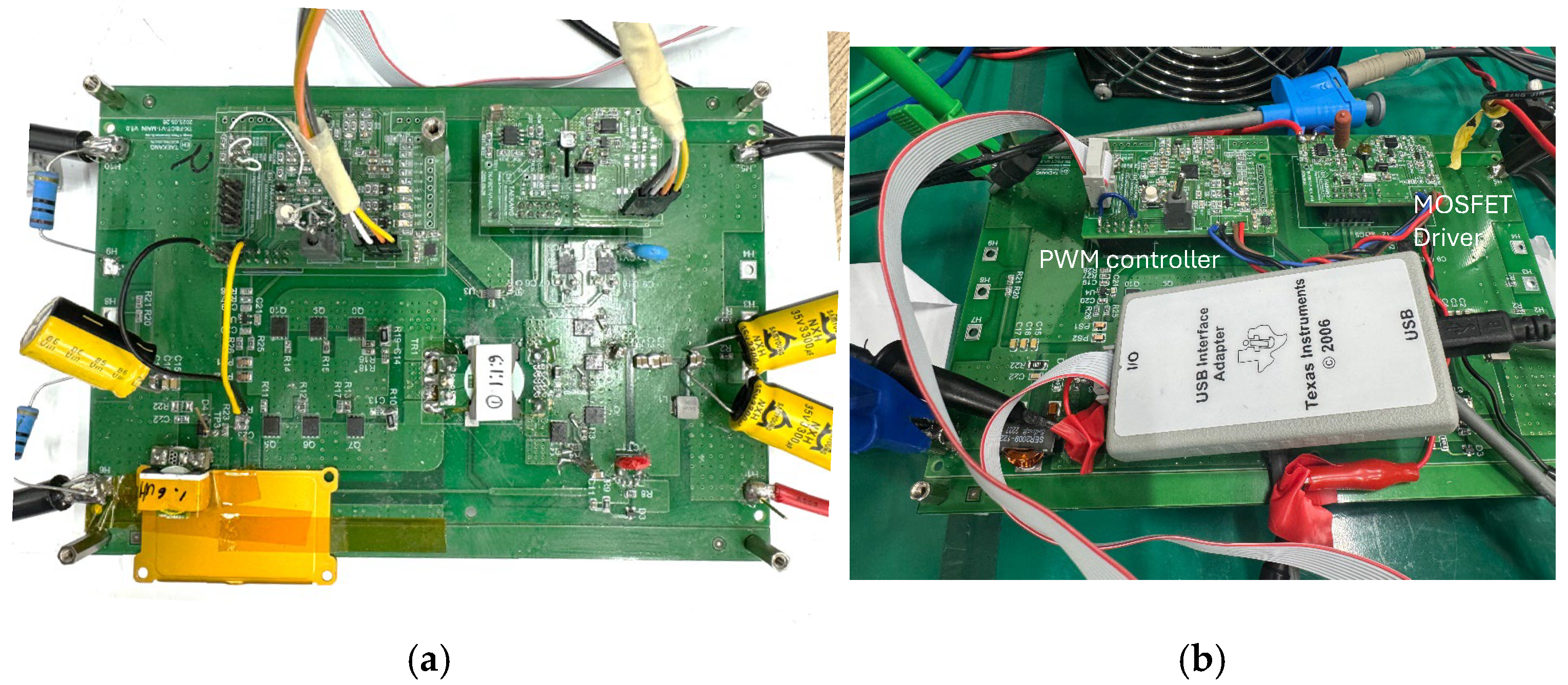
Figure 5 illustrates the equivalent circuit of the full-bridge converter, incorporating internal parasitic resistances. Each resistance represents a component that contributes to conduction loss, such as the on-resistance of the switches and the winding resistance of the transformer. As indicated in (22), the power dissipation caused by these parasitic resistances is reflected in the loss coefficient K 2 . Table 5 details the specifications of the primary components used in the experimental prototype. For the main switches S 1,2 , 3,4 of the full-bridge converter, low-loss FETs (FDM86101 from Onsemi, Phoenix, AZ, USA) were employed. For the synchronous rectifier switches S A , B , BSC026N08NSS from Infineon (Neubiberg, Germany) was selected because of its low on-resistance and low-profile package. While the proposed model demonstrates high accuracy, certain limitations exist regarding the selection of specific components. The Infineon (Neubiberg, Germany) BSC026N08NSS MOSFET used in this experiment features extremely low on-resistance and an optimized low-profile package; therefore, applying general-purpose components with lower performance specifications may lead to variations in the power loss model coefficients. The main switches feature a rated voltage of 100 V, an on-resistance of 80 mΩ, and an internal parasitic capacitance of 0.5 nF. TDK magnetic cores were used for both the transformer and the inductor. Notably, the windings were designed using PCB patterns, which significantly reduced the overall height of the system. Table 6 lists the parasitic parameter values of the key components; these values were primarily sourced from the manufacturers’ datasheets, while the parameters for the transformer and inductor were obtained through direct measurement. For experimental measurements, a Takasago (Japan) ZX-800LA (800 W) DC power supply and a Keisokugiken (Japan) LN-1000C-G7 (1 kW) electronic load were utilized. Power analysis was performed using a Yokogawa (Japan) WT1600 power meter. Operational waveforms were observed with a Teledyne LeCroy (New York, USA) HDO6104 oscilloscope, complemented by AP015 current probes and HVD3106 differential probes. Figure 6 presents the configuration of the experimental circuit and the measurement setup. In particular, the control stage utilized a TI (Dallas, TX, USA) UCD3138 digital controller to ensure flexibility and scalability for the system.

5. Comparative Analysis of Experimental Circuits

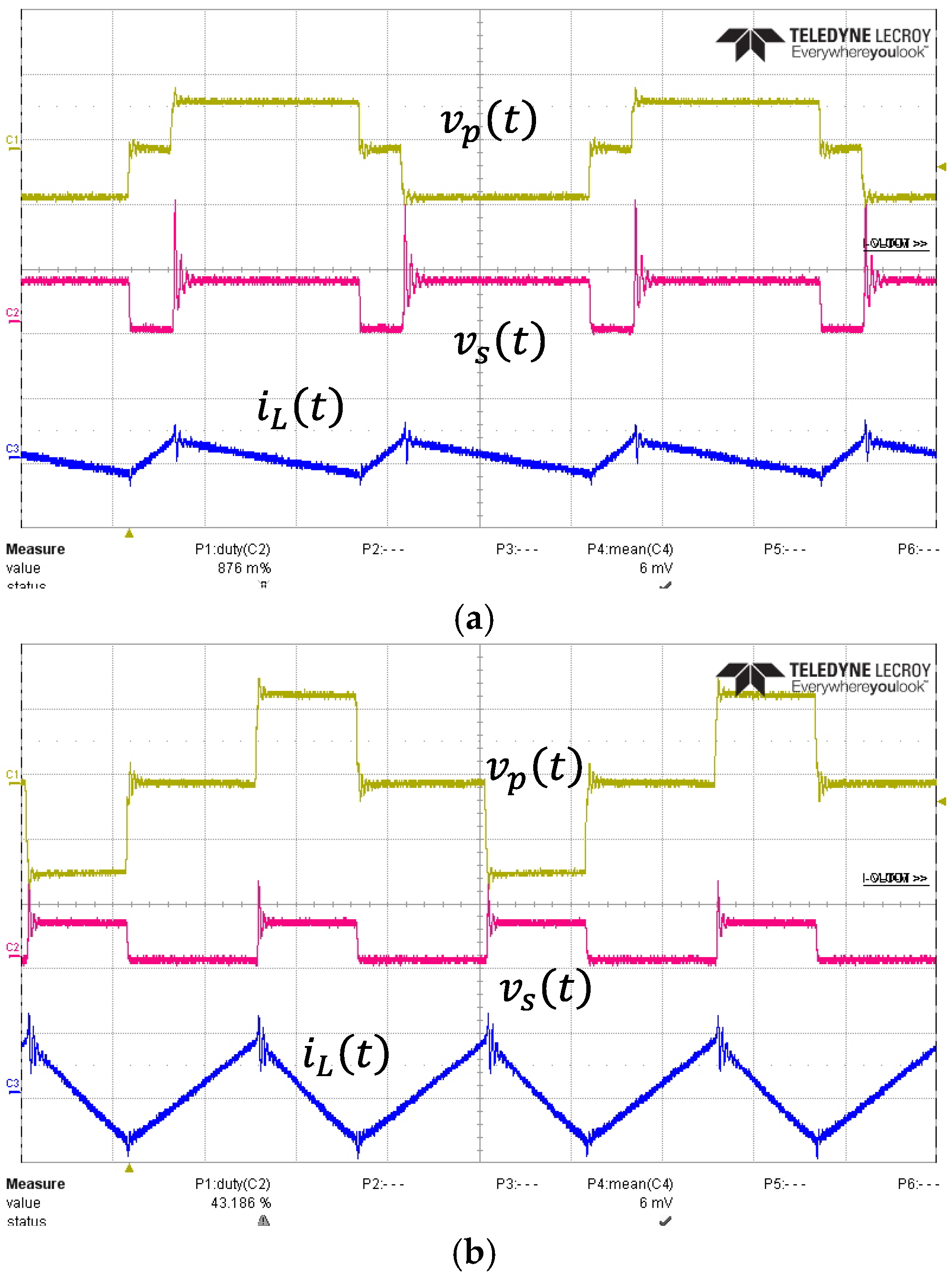
Figure 7 illustrates the primary operational waveforms of the experimental full-bridge converter. The measurements were conducted at a load current of 15 A with input voltages of 38 V and 70 V. From top to bottom, the waveforms represent the transformer primary voltage, the secondary-side synchronous rectifier switch voltage, and the output inductor current. As shown in the figure, at the minimum input voltage of 38 V, a wide switching interval is observed, which is attributed to the duty cycle compensation for low input voltage conditions. Conversely, while the duty cycle is at its minimum when the input voltage is 70 V, the amplitude of the inductor current ripple reaches its peak. Furthermore, since the AC component of the inductor current flows through the capacitor, the conduction loss of the output capacitor is expected to be highest at an input voltage of 70 V.
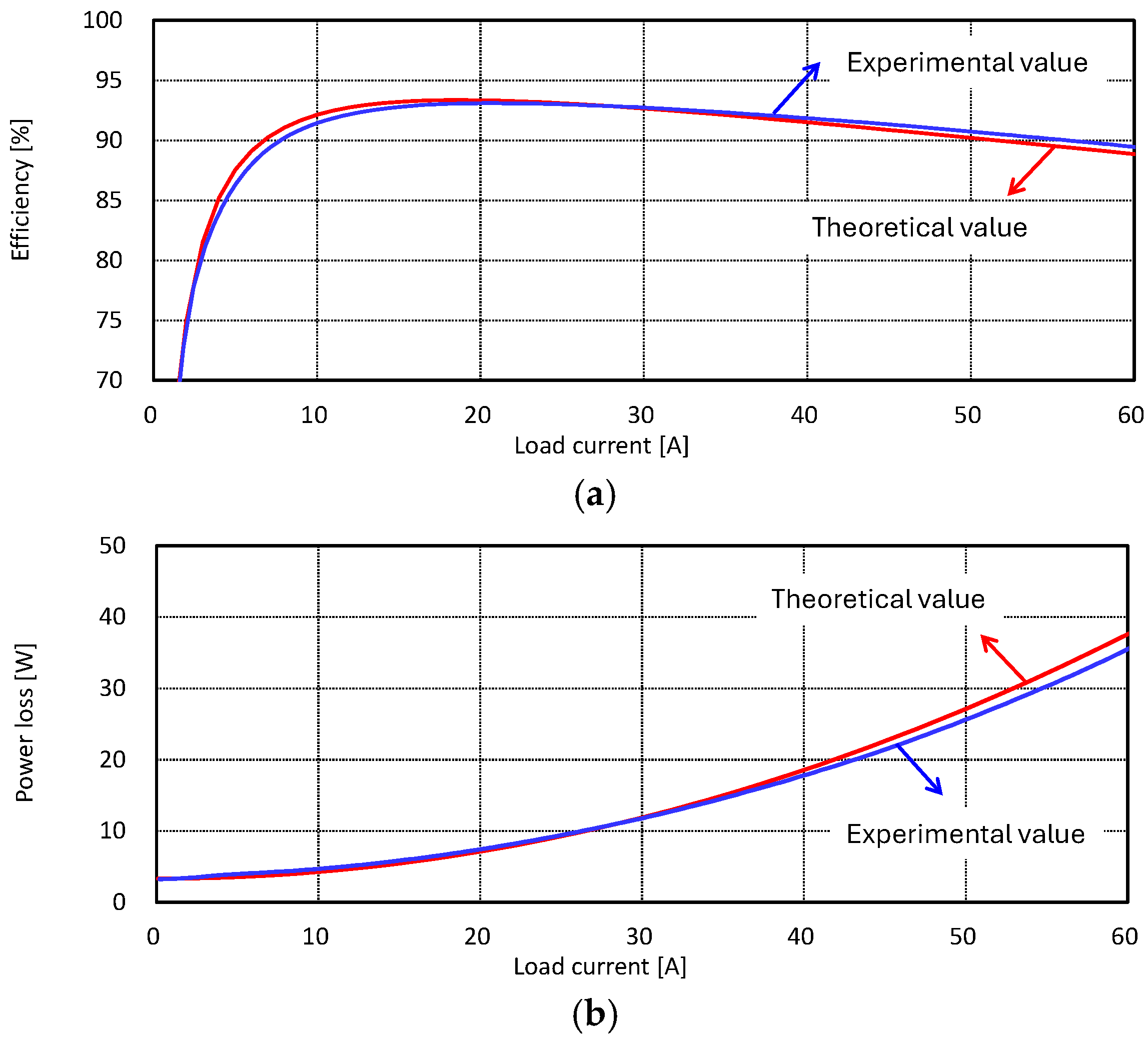
The following graphs present the analysis of the internal losses and efficiency characteristics of the 300 W prototype. Figure 8 shows the power conversion efficiency and internal power loss analyzed at the minimum input voltage of 34 V. In Figure 8a, the power conversion efficiency is compared between the theoretical and experimental values. The theoretical values were calculated using (22) and (23), while Figure 8b depicts the internal power loss. The maximum efficiency recorded was 93.11%, with a maximum internal loss of 37.6 W. Specifically, at full load, the theoretical and experimental efficiencies were 89.42% and 88.9%, respectively; overall, the efficiency and loss curves exhibited a very similar trend with a maximum deviation of less than 1%. To evaluate the scientific accuracy of the proposed model, a detailed comparative examination was conducted across specific load segments. As requested by the reviewer, the efficiency trends were analyzed to identify discrepancies between theoretical and practical values. In the light-load region (0–15 A), the efficiency predicted by the theoretical model was slightly higher than the practically measured values. This minor discrepancy is attributed to the increased dominance of auxiliary power consumption and parasitic switching losses that are challenging to characterize fully at very low currents. Conversely, in the medium-to-full load range (30–60 A), the theoretical efficiency was observed to be slightly lower than the practical results in certain points, although the curve closely tracked the measured data overall.
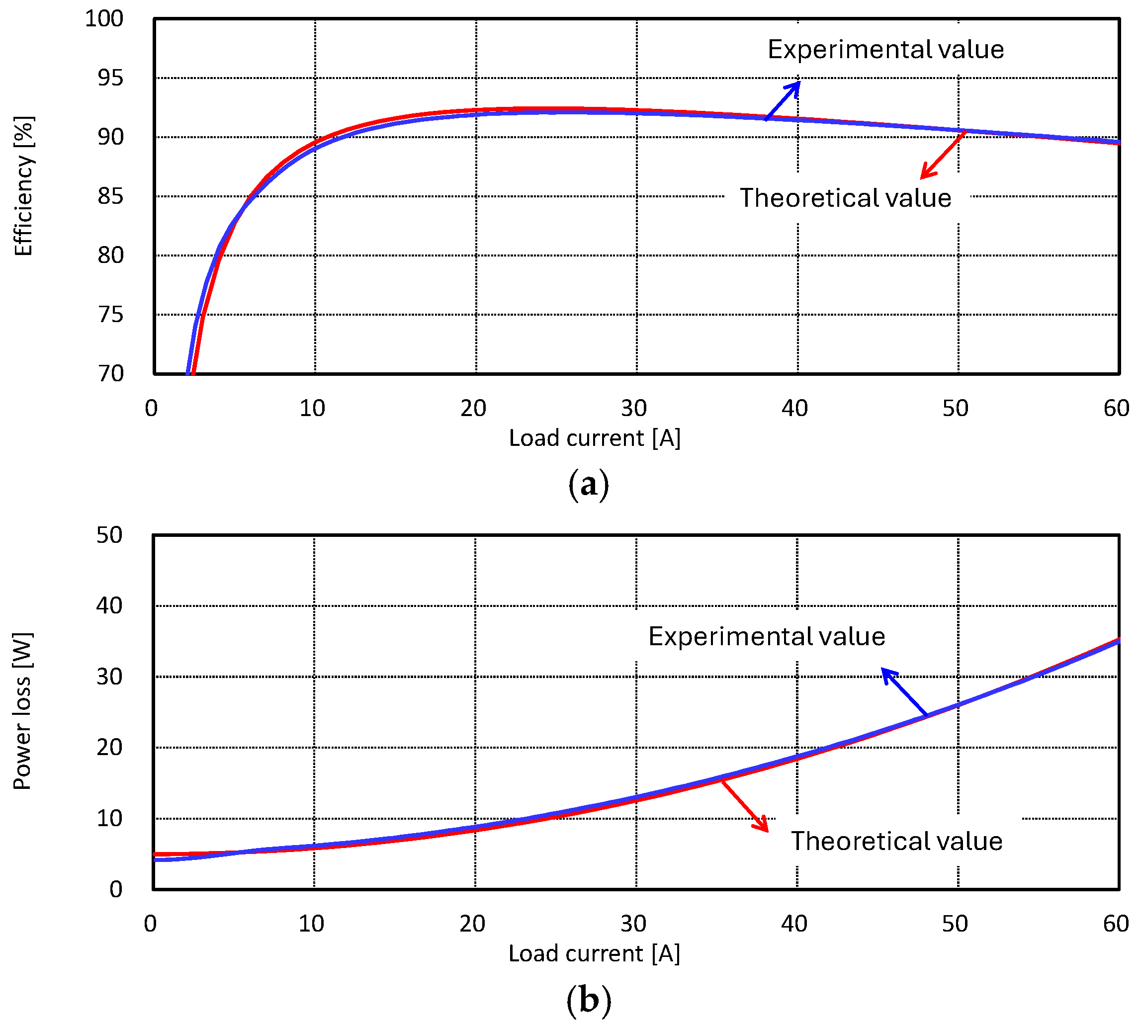
Such anomalies between theory and practice are well-recognized in power electronics research due to the complex nonlinear behavior of components under varying thermal and electromagnetic conditions. However, the maximum error margin between the calculated and measured efficiency remained below 1.0% across the entire load spectrum. Given that a tolerance limit of 1% to 5% is generally accepted in literature as a standard for validating scientific accuracy, the results presented in Figure 8 and Figure 9 confirm that the proposed loss-coefficient-based framework is highly reliable. Specifically, Figure 9 illustrates the comparative analysis at a nominal input voltage of 48 V. As depicted in Figure 9a,b, the converter achieved a measured maximum efficiency of 92.1%. At the 100% rated load, the theoretical efficiency of 89.6% aligns exceptionally well with the experimental value of 89.7%, resulting in a negligible discrepancy of only 0.1%. This high degree of correlation, with error margins well below the 1–5% permissible limit, demonstrates that the proposed methodology effectively captures the impact of both constant losses and load-dependent conduction losses.
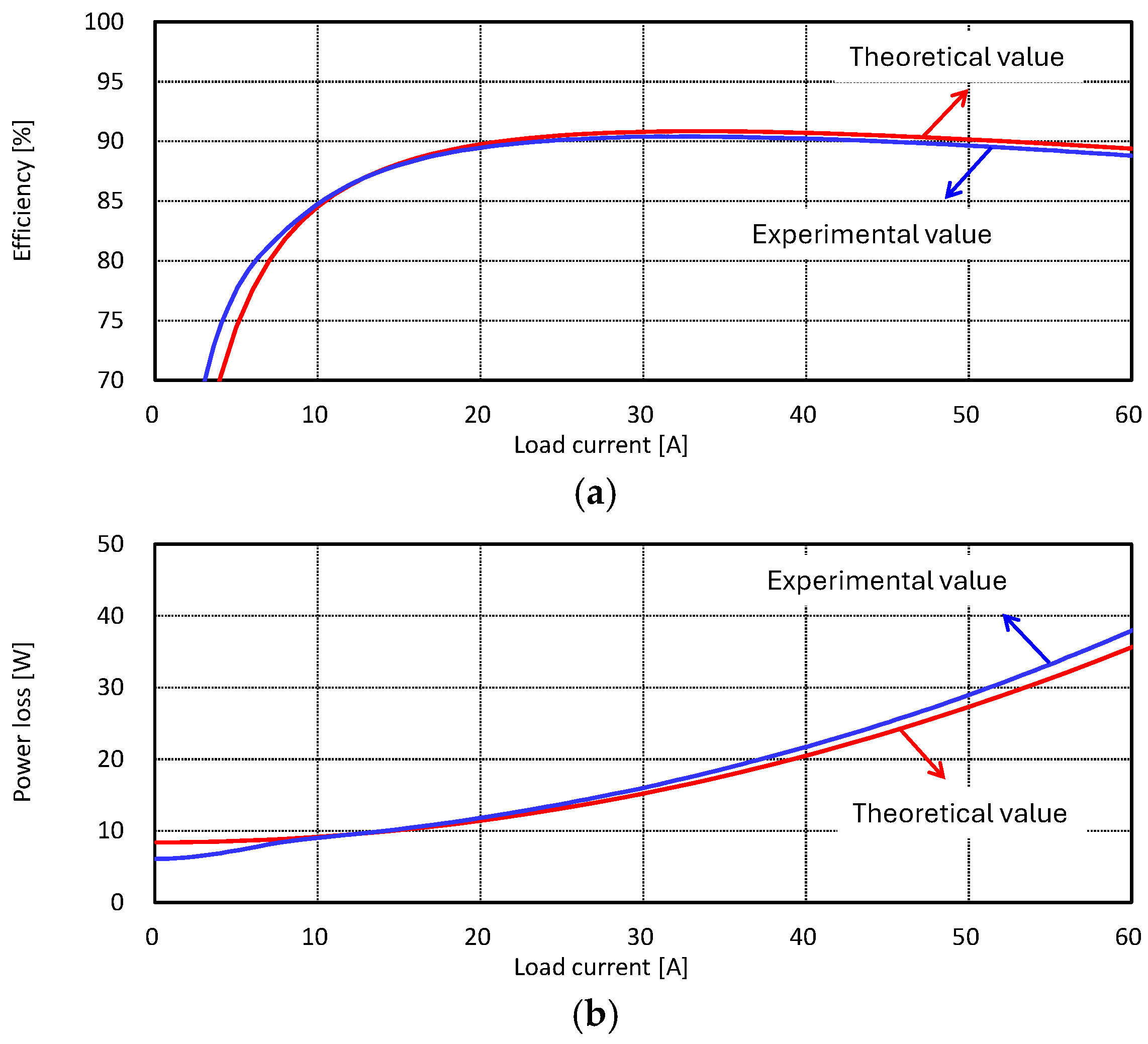
Figure 10 illustrates the performance at the maximum input voltage of 70 V. The maximum efficiency was 90.4%, with a maximum internal loss of 37.72 W. Although the theoretical and experimental efficiencies at full load were 89.4% and 88.8%, respectively, the curves maintained a similar profile within a 1% error margin. The proposed model’s accuracy was rigorously tested across a wide load spectrum. As depicted in Figure 8, Figure 9 and Figure 10, the efficiency analysis includes light-load data points (such as 10% and 20% of the rated load), where the theoretical curves closely align with the experimental measurements with an error of less than 1%. This consistency validates that the loss coefficients effectively capture both constant and load-dependent losses.
The data show that power conversion efficiency and internal power loss at 34 V, 48 V, and 70 V input differ by less than 1% between experimental and theoretical values. Furthermore, the internal loss and efficiency curves demonstrated consistent trends across the entire load current range. The proposed loss coefficient analysis method, which uses the RMS currents of major components and internal parasitic elements, effectively predicts internal power loss and efficiency at the initial design stage.

6. Conclusions

In this paper, a novel analytical approach is proposed for the precise and systematic evaluation of power conversion efficiency in full-bridge converters. A steady-state analysis was conducted based on the equivalent circuit of the full-bridge converter, leading to the introduction of the “Loss Coefficient” concept. This concept redefines loss factors based on their correlation with load power and load current. Specifically, to clarify the impact on overall system efficiency, loss coefficients originating from major active and passive components were categorized according to their dependence on the load current. These coefficients were tabulated to provide a quantitative breakdown of the loss distribution. Furthermore, beyond mathematical derivation, this study visualized the correlation between internal losses and overall power conversion efficiency through graphical representations. These intuitive graphs enable designers to easily identify loss distributions and facilitate the achievement of optimal efficiency.
To verify the effectiveness and reliability of the proposed analytical technique, a 300 W full-bridge converter prototype was fabricated and tested. The theoretically derived loss and efficiency analysis results were quantitatively compared with the data measured from the experimental circuit. The results demonstrate that under full-load conditions, the error between theoretical and experimental efficiency values remained within a very narrow margin of less than 1%. This confirms that the analytical model proposed in this study accurately reflects the operational characteristics of the actual hardware. In conclusion, the loss coefficient analysis method incorporating the RMS currents of key components and internal parasitic elements has proven to be a highly effective means of predicting internal power loss trends and power conversion efficiency characteristics relative to load current variations. The proposed loss coefficient-based analysis provides a versatile framework that can be extended to various isolated DC–DC converter topologies, provided that the RMS current relations of the components are established. While this study focused on fixed-frequency full-bridge converters, future research will explore the adaptation of this model to frequency-modulated systems, further enhancing its applicability in diverse power conversion scenarios.

Author Contributions

Conceptualization, T.A.; methodology, H.J., M.C. and T.A.; validation, H.J., M.C. and T.A.; formal analysis, T.A.; investigation, H.J. and M.C.; resources, T.A.; data curation, M.C. and T.A.; writing—original draft preparation, H.J., M.C. and T.A.; writing—review and editing, H.J., M.C. and T.A.; visualization, H.J. and T.A.; supervision, H.J. and T.A.; project administration, M.C. and T.A.; funding acquisition, T.A. All authors have read and agreed to the published version of the manuscript.

Funding

This research was supported by the Regional Innovation System & Education (RISE) program through the Chungbuk Regional Innovation System & Education Center, funded by the Ministry of Education (MOE) and the Chungcheongbuk-do, Republic of Korea (2025-RISE-11-013-03).

Data Availability Statement

The original contributions presented in this study are included in the article. Further inquiries can be directed to the corresponding authors.

Conflicts of Interest

Author Myeonghun Cho was employed by the company Taekang Inc. The remaining authors declare that the research was conducted in the absence of any commercial or financial relationships that could be construed as a potential conflict of interest. The remaining authors declare that the research was conducted in the absence of any commercial or financial relationships that could be construed as a potential conflict of interest.

Abbreviations

The following abbreviations are used in this manuscript:
BMSbattery management system
ESRequivalent series resistance
EVelectric vehicle
MOSFETmetal oxide semiconductor FET
PCBprinted circuit board
RMSroot mean square
SRsynchronous rectifier
TDKTokyo Denki Kagaku
TITexas instruments
WBGwide bandgap
ZVSzero voltage switching
V I N input voltage
V o output voltage
I o load current
P o output power
P T total power loss
f s switching frequency
D duty cycle
n transformer turns ratio
r o n MOSFET on-state resistance
r A synchronous rectifier on-resistance
r L inductor DC resistance
K 0 constant loss coefficient
K 1 linear loss coefficient
K 2 quadratic loss coefficient
η power conversion efficiency

References

  1. Zhao, L.; Li, H.; Yu, Y.; Wang, Y. A Novel Choice Procedure of Magnetic Component Values for Phase Shifted Full Bridge Converters with a Variable Dead-Time Control Method. Energies 2015, 8, 9655–9669. [Google Scholar] [CrossRef] [Scilit]
  2. Tran, D.; Vu, N.; Choi, W. A Quasi-Resonant ZVZCS Phase-Shifted Full-Bridge Converter with an Active Clamp in the Secondary Side. Energies 2018, 11, 2868. [Google Scholar] [CrossRef] [Scilit]
  3. Tran, D.; Tran, M.; Choi, W. A Hybrid Soft Switching Full Bridge Converter Suitable for Wide Load Range Applications. Energies 2018, 11, 3236. [Google Scholar]
  4. Wang, Y.; Sun, F.; Chen, J.; Cai, H.; Gao, S. Novel Series-Parallel Phase-Shifted Full-Bridge Converters with Auxiliary LC Networks to Achieve Wide Lagging-Leg ZVS Range. Electronics 2024, 13, 1311. [Google Scholar] [CrossRef] [Scilit]
  5. Chen, W.; Wu, X. A Novel Hybrid Full-Bridge Converter for Wide Input Voltage Range Applications. Energies 2013, 6, 2841–2856. [Google Scholar]
  6. Kim, J.-W.; Moon, G.-W. A New Soft-Switching Phase-Shifted Full-Bridge Converter with Reduced Circulating Loss and Voltage Stress. Energies 2016, 9, 820. [Google Scholar]
  7. Li, X.; Wang, S. An Improved Full-Bridge DC-DC Converter with Wide ZVS Range and Reduced Circulating Current. Electronics 2023, 12, 987. [Google Scholar]
  8. Zhang, Y.; Liu, C. Efficiency Optimization for Phase-Shifted Full-Bridge Converter in Data Center Power Supply. Energies 2022, 15, 1123. [Google Scholar]
  9. Wang, L.; Zhang, Z. Accuracy Loss Modeling of Phase-Shifted Full-Bridge Converters for Electric Vehicle Chargers. Energies 2021, 14, 3567. [Google Scholar]
  10. Park, S.-S.; Choi, S. Soft-Switching Bidirectional Full-Bridge Converter for Battery Energy Storage Systems. Energies 2020, 13, 2054. [Google Scholar]
  11. Xu, G.; Wang, J. A Load-Adaptive Phase-Shift Control Method for Efficiency Improvement of Full-Bridge Converters. Electronics 2021, 10, 1842. [Google Scholar]
  12. Feng, W.; Lee, F.C. Optimal Trajectory Control of LLC Resonant Converters for Soft Start-Up. IEEE Trans. Power Electron. 2014, 29, 1461–1468. [Google Scholar] [CrossRef] [Scilit]
  13. Mohseni, P.; Husev, O.; Kasper, M.; Deboy, G. Design Optimization for Enhancing the Power Density and Efficiency for GaN-Based DC–DC Converter. IEEE Trans. Ind. Electron. 2025, 72, 10189–10203. [Google Scholar] [CrossRef] [Scilit]
  14. Li, M.; Deng, J.; Zhang, Z.; Wang, Z. A Hybrid Modulation Strategy Based on Tandem-Half-Bridge WPT Converter for Efficiency Optimization Within Wide Operation Range. IEEE Trans. Power Electron. 2024, 39, 4824–4836. [Google Scholar] [CrossRef] [Scilit]
  15. Jung, B.; Lee, J.; Choi, J.; Kim, Y. Analytical Loss Minimization Control for IPMSM Using Linearized Torque and Loss Modeling. IEEE Access 2026, 14, 2224–2235. [Google Scholar] [CrossRef] [Scilit]
  16. Wang, K.; Laird, I.; Wang, J.; Yan, J.; Xu, W. Efficiency-Oriented Multi objective Modulation Optimization for the Dual Active Bridge Converter Using Fuzzy Logic-Aided Strategy. IEEE Trans. Power Electron. 2025, 40, 18133–18147. [Google Scholar] [CrossRef] [Scilit]
  17. Zhao, W.; Yang, Y.; Qian, T. A Soft-Switching Boost-Type Resonant Forward Converter with Load-Adaptive Efficiency Optimization. IEEE Trans. Circuits Syst. I Regul. Pap. 2025, 72, 4359–4369. [Google Scholar] [CrossRef] [Scilit]
  18. Hassan, Z.; Selvaraj, J.; Ismail, F.; Shah, N.A.M. High-Efficiency Bidirectional CLCLC Resonant DC–DC Converter with Soft-Switching Performance and Stability Optimization. IEEE Access 2026, 14, 10002–10022. [Google Scholar] [CrossRef] [Scilit]
  19. Hirata, A.; Takagi, S. Modeling of Human Body Shadowing Loss at 300 GHz Based on Measurement of Path Loss and Direction of Arrival. IEEE Trans. Antennas Propag. 2025, 73, 1162–1172. [Google Scholar] [CrossRef] [Scilit]
  20. Yang, D.; Wang, B.; Shao, S.; Zhang, J. High-Frequency Transformer Loss Measurement and Modeling: A DC Loss Method. IEEE Trans. Power Electron. 2025, 40, 5635–5645. [Google Scholar] [CrossRef] [Scilit]
  21. Lee, Y.C.; Park, M.-S.; Jang, W.; Oh, S. Frequency-Dependent Window Penetration Loss and Its Relation to Building Entry Loss Models. IEEE Wirel. Commun. Lett. 2026, 15, 510–514. [Google Scholar]
  22. Zhou, L.; Zhang, J.; Zhang, J.; Qiu, K. An Environment-Adaptive Radio Propagation Path Loss Model with Ray-Based Validation. IEEE Antennas Wirel. Propag. Lett. 2024, 23, 3217–3221. [Google Scholar] [CrossRef] [Scilit]
  23. Ethier, J.; Châteauvert, M. Machine Learning-Based Path Loss Modeling with Simplified Features. IEEE Antennas Wirel. Propag. Lett. 2024, 23, 3997–4001. [Google Scholar] [CrossRef] [Scilit]
  24. Hagedorn, M.; Rettner, C.; Korn, M.; Mertens, A. Time-Efficient Power Loss Calculation for Battery-Electric Powertrains Based on Harmonic Loss Models. In Proceedings of the 2024 27th International Conference on Electrical Machines and Systems (ICEMS); IEEE: Washington, DC, USA, 2025; pp. 914–920. Available online: https://ieeexplore.ieee.org/document/10836940 (accessed on 16 January 2026).
  25. Sauter, B.; Reese, S.; Sinha, S.; Haddon, J.; Byrd, T.; Maksimovic, D. Integrating Equation-Based Methods with Random Forest Regression for Improved Accuracy of Magnetic Core Loss Modeling. In Proceedings of the 2024 IEEE Applied Power Electronics Conference and Exposition (APEC); IEEE: Washington, DC, USA, 2024; pp. 410–415. Available online: https://ieeexplore.ieee.org/document/10509376 (accessed on 16 January 2026).
  26. Luo, S.; He, G.; Hou, N. Reflux Power Optimization of a Dual-Active Hybrid Full-Bridge Converter Based on Active Disturbance Rejection Control. Energies 2024, 17, 4299. [Google Scholar] [CrossRef] [Scilit]
  27. Guo, X.; Meng, R.; Bai, X.; Li, H.; Zhang, J.; He, X. Study of Improved Active Clamp Phase-Shifted Full-Bridge Converter. Electronics 2025, 14, 834. [Google Scholar] [CrossRef] [Scilit]
Figure 1. Basic circuit of a full bridge DC–DC converter.
Energies 19 00899 g001
Figure 2. Equivalent circuit of a full bridge DC–DC converter.
Energies 19 00899 g002
Figure 3. Steady-state equivalent circuits by operating mode: (a) Equivalent circuit in state 1, (b) Equivalent circuit in state 2, (c) Equivalent circuit in state 3, and (d) Equivalent circuit in state 4.
Energies 19 00899 g003
Figure 4. Main operating waveforms in steady state [2,3].
Energies 19 00899 g004
Figure 5. Internal parasitic resistance and equivalent circuit.
Energies 19 00899 g005
Figure 6. Experimental circuit and experiment configuration photo. (a) Experimental circuit configuration. (b) PWM controller and experimental circuit configuration.
Energies 19 00899 g006
Figure 7. Comparison of steady-state switch voltage and current of full bridge DC–DC converter. (a) Operating waveform at 38 V input voltage and 15 A load current. (b) Operating waveform at 70 V input voltage and 15 A load current.
Energies 19 00899 g007
Figure 8. Comparison of power conversion efficiency and internal power loss for load current at 34 V input. (a) Power conversion efficiency. (b) Internal power loss.
Energies 19 00899 g008
Figure 9. Comparison of power conversion efficiency and internal power loss for load current at 48 V input. (a) Power conversion efficiency. (b) Internal power loss.
Energies 19 00899 g009
Figure 10. Comparison of power conversion efficiency and internal power loss for load current at 70 V input. (a) Power conversion efficiency. (b) Internal power loss.
Energies 19 00899 g010
Table 1. Characteristic equation and RMS current in steady state.
ParameterValueUnit
Voltage gain M N V o V I N = 2 D
Turns ratio N 2 D   V I N V o
Minimum duty ratio D m i n N   V o 2 V I N   m a x
Transformer primary RMS current I T   r m s I o 2 D N 1 + 1 48 N 2 V o I o f s 2 1 L M + 1 2 D N 2 L F 2
Transformer secondary RMS current I S   r m s I o 2 1 + 2 D
Main switch RMS current I s 1   r m s I o D N 1 + 1 48 N 2 V o I o f s 2 1 L M + 1 2 D N 2 L F 2
SR switch RMS current I S A   r m s I o 2 1 + 2 D
Inductor RMS current I L   r m s I o 1 + 1 2 D 2 48 V o I o L F f s 2
Capacitor RMS current I C   r m s V o 1 2 D 48 f s L F
Transformer ripple current i T V o N 2 f s 1 L M + 1 2 D N 2 L F
Inductor ripple current i L V o 1 2 D 2 L F f s
Magnetizing ripple current i M N V o 2 L M f s
Maximum magnetizing current I M   m a x N V o 4 L M f s
Maximum inductor current I L   m a x I o + V o 1 2 D 4 L F f s
Maximum transformer current I T m a x I o N + V o N 4 f s 1 L M + 1 2 D N 2 L F
Output capacitance C o V o 1 2 D m i n 32 f s 2 L F V c p p
Output inductance L F V o 1 2 D m i n 4 f s I o   m i n
Magnetizing inductance L M 9 N 2 L F V o 4 L F f s I o   m a x + V o 1 2 D m i n
Table 2. Power loss of major components related to loss coefficient K 0 .
ParameterValueUnit
Main switch switching loss P F B _ s w 1 2 · V i n 2 · C F B · f s × 4
SR switch switching loss P S R _ s w 1 2 · V i n N 2 · C S R · f s × 2
Transformer magnetic core loss P c o r e T 5.88 × 10 7 · B m 2.7 · f s 2.12 · V e
Inductor magnetic core loss P c o r e L 3.50 × 10 6 · B m 2.5 · f s 1.4 · V e
Output capacitor esr loss P c o 1 48 V o 1 2 D f s L F 2 · r e s r
Table 3. Power loss of major components related to loss coefficient K 2 .
ParameterValueUnit
Main switch conduction loss P F B _ c o n d D N 2 I o 2 + 1 48 N 2 V o f s 2 1 L M + 1 2 D N 2 L F 2 · r F B · 4
SR switch conduction loss P S R _ c o n d 1 + 2 D 4 · r S R · 2
Transformer conduction loss P T 1 _ c o n d 2 D N 2 1 + 1 48 N 2 V o I o f s 2 1 L M + 1 2 D N 2 L F 2 · r T 1
Transformer conduction loss P T 2 _ c o n d 1 + 2 D 4 · r T 2 · 2
Inductor wire conduction loss P L _ c o n d 1 + 1 2 D 2 48 V o I o L F f s 2 · r L
Table 4. Electrical specifications of the experimental circuit.
Parameter ValueUnit
Input voltage range V I N 36–75Vdc
Output voltage V o 5.0Vdc
Maximum output power P o   m a x 300W
Maximum output current I o   m a x 60A
Switching frequency f s 240 kHz
Efficiency η 90%
Table 5. Manufacturer and model of main components.
ParameterNameModelMaker
Main switch S 1 4 FDMS86101Fairchild (TX, USA)
SR switch S A , B FDMS86101Fairchild (TX, USA)
Transformer T 1 PA0908NLPulse (CA, USA)
Inductor L F SER2814HCoilcraft (IL, USA)
Capacitor C F 47µFMurata (Japan)
Table 6. Parasitic element values of key elements.
ParameterUnitValue
InductanceμH140
Cross-sectional area of corecm20.12
Volume of corecm33.4
Wire resistance20
Switch capacitancenF0.5
Switch on resistance80
Capacitor ESR Ω0.4
Auxiliary powerW1.0
Disclaimer/Publisher’s Note: The statements, opinions and data contained in all publications are solely those of the individual author(s) and contributor(s) and not of MDPI and/or the editor(s). MDPI and/or the editor(s) disclaim responsibility for any injury to people or property resulting from any ideas, methods, instructions or products referred to in the content.