Article

Current-Summing Multilevel LCC Inverter for Radiated EMI Harmonic Reduction in Wireless Power Transfer


Department of Electrical Engineering, Incheon National University, Incheon 22012, Republic of Korea
*
Author to whom correspondence should be addressed.
Energies 2026, 19(4), 1063; https://doi.org/10.3390/en19041063
Submission received: 13 January 2026 / Revised: 10 February 2026 / Accepted: 13 February 2026 / Published: 19 February 2026
(This article belongs to the Section F3: Power Electronics)

Abstract

This article proposes a parallel current-summing LCC multilevel inverter (MLI) to suppress harmonic distortion of radiated EMI for wireless power transfer. Traditionally, ZVS has been an issue for staircase voltage output multilevel inverters because a shared current output became faster than some of the voltage transitions in staircase voltage output. The other common problem was capacitor voltage imbalance and resultant output voltage distortion if a sophisticated voltage balancing function is not used. The proposed LCC MLI ensures ZVS by separating each voltage transition into multiple bridge legs. Each bridge leg outputs different phases of currents for each voltage transition. The individual output currents are summed at the matching network of wireless power transfer, generating a near-sinusoid output current to suppress harmonic distortions. In this way, each leg achieves ZVS even though the summed output current at the LCC network is faster than some of the voltage transitions. To avoid the capacitor voltage imbalance issue, the proposed MLI eliminated the flying capacitor. Instead, the four parallel legs are supplied by a shared DC input link. Therefore, the four legs can output identical voltages without using a typical DC flying capacitor. The necessity of multiple input voltage sources is, therefore, also eliminated. Measurement demonstrates that the proposed method effectively reduces radiated harmonic EMI by up to 14 dB.

1. Introduction

In inductive wireless power transfer (WPT), international regulation specifies an upper limit for the radiated magnetic field strength or electromagnetic interference (EMI). In Korean regulations, for example, the radiation of the third and fifth harmonics should be 57.78 dB and 61.24 dB below that of the fundamental 85 kHz [1]. Harmonic distortion in coil current should be reduced to suppress EMI radiation because the loosely coupled coil emits the majority of the magnetic field [2,3].
To solve this problem, many techniques have been proposed to reduce the harmonics in the squarewave inverter. Using additional filters is one of the techniques to reduce harmonics. However, the problem is the efficiency drop of 1.1% and 10% [4,5] due to the added filters. Magnetic materials like Ferrite and Nanocrystalline can shield the nearby metal casing frames from the magnetic field [6,7]. However, there still exists a significant open air gap between the TX coil and the RX coil, and this open air gap cannot be sealed by materials due to the application scenario of WPT, which requires clearance as wide as possible. While the nearby frames can be protected by Ferrite or Nanocrystalline, significant magnetic field leakage through the open air gap still radiates into the air. Adjusting and optimizing load resistance helps to suppress harmonic current [8]. However, it requires a dc/dc converter at the receiver side.
A multilevel inverter (MLI) is an attractive solution to reduce harmonic current. The multilevel inverters reduce harmonic distortion by generating a staircase output voltage that mimics an ideal sinusoid better than the squarewave output voltage [9,10,11,12,13,14,15]. While MLIs using flying capacitors (FCs) or neutral point clamped (NPC) capacitors are popular, they require voltage balancing control. Meanwhile, multiple DC source type MLIs use series-stacked bridge stages [10,11,16], where the multiple isolated DC voltage sources are not practical.
More importantly, regardless of FC, NPC, or series-stacked bridge MLI, they fail ZVS when it is used to generate staircase voltage output, which has multiple transitions within a period. This is because the same inverter current flows through different MOSFETs [9,10,11,12,13]. For example, [13] illustrates the ZVS turn-on failure issue at some rising edge transitions of the staircase output. This is because, in order to form multiple transitions of staircase outputs, the switch has to turn on at the moment when the output current has positive polarity. This will be discussed in Section 2 and Figure 1 of this paper.
Some MLIs for wireless power transfer successfully achieve ZVS in [17,18,19]. The modular multilevel topology is presented in [18,19]. They sum voltages across each flying capacitor or across series-connected submodules. The summation is performed in-phase by turning on selected submodules or MOSFETs at the same time. This can generate a squarewave voltage whose amplitude can be varied by the number of selected submodules. Therefore, although they achieve ZVS, they do not generate the staircase output voltage, which is necessary to reduce harmonic distortion EMI. The voltage balancing control for flying capacitors is also still necessary.
To address these problems, this paper proposes a parallel current-summing multilevel inverter for LCC-compensated wireless power transfer. This inverter introduces separate bridge leg outputs. Each leg generates a different phase of output voltage and current. The two currents of different phases from each leg are summed by the LCC impedance-matching inductors of wireless power transfer. The phase of voltage transition in each leg is faster than the phase of its MOSFET current, which achieves ZVS for all bridges. Other benefits are that only a single DC input source is used and that capacitor voltage balancing is not necessary. Table 1 compares the characteristics of different MLI topologies.

2. Typical Staircase MLI in WPT

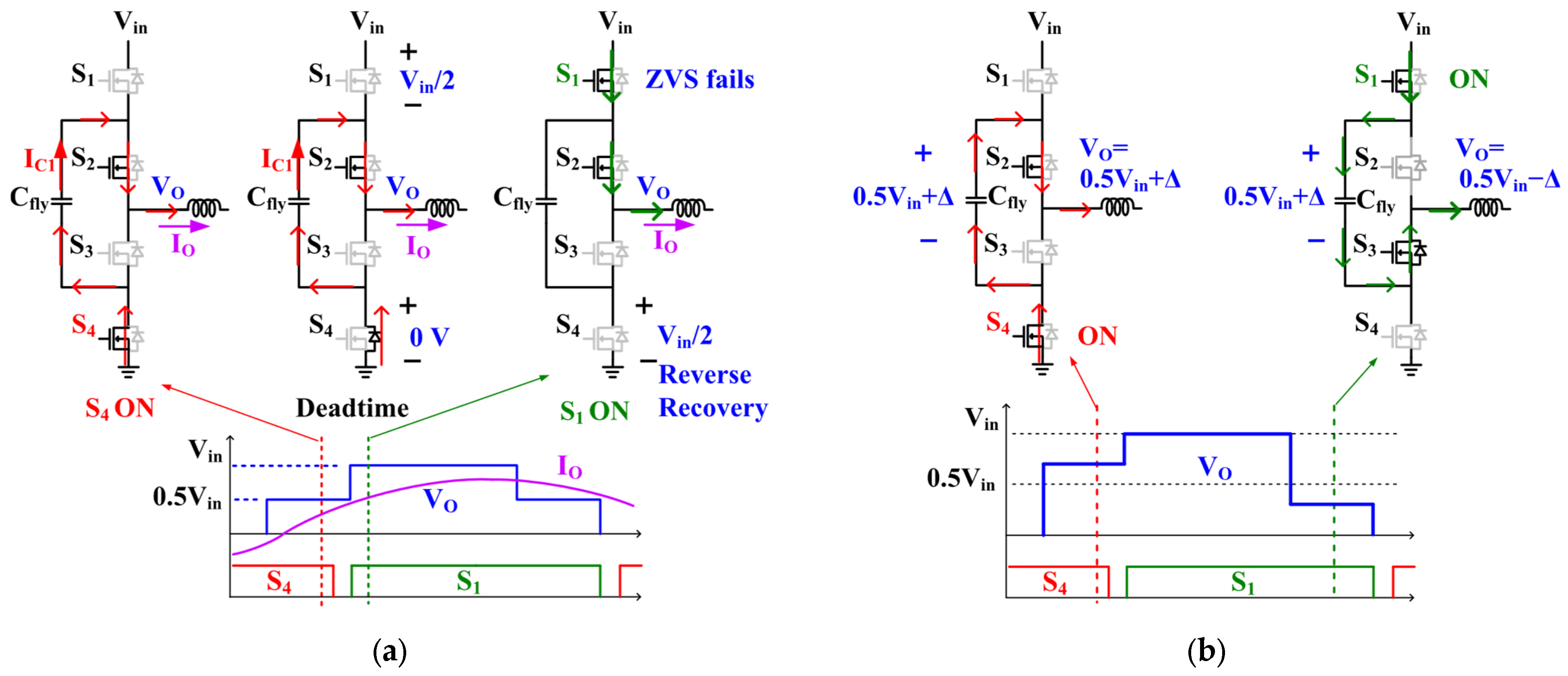
Figure 1a illustrates the ZVS failure issue of a typical MLI when it is generating staircase VO. Although Figure 1 represents a schematic of an FC MLI, the output waveform is applicable to other topologies of MLIs, as in [11,13]. The series-connected MOSFETs carry the same output current IO, and the polarity of IO is positive at highlighted timings. Therefore, during the dead time between S4 and S1, the current cannot flow through the body diode of S1. The S1 fails ZVS turn-on, and the body diode of S4 turns off with reverse recovery loss. ZVS failure at the VO transition from half Vin to full Vin is also discussed in other topologies, such as [13].
This problem occurs because the same IO flows through every MOSFET, while each MOSFET should turn on at different times to generate a staircase VO output, which has multiple rising edges. For applications that do not generate staircase VO output, as in [17,18,19], ZVS failure issue does not occur. However, in the proposed work, the goal is to reduce the harmonic distortion to mitigate radiated EMI, and, therefore, the staircase sinusoid-mimicking output is necessary.
Figure 1b illustrates the voltage imbalance issue. Due to the nonideal asymmetry of each transition, the DC voltage of capacitor Cfly cannot develop the precise half of Vin. This nonideality causes distortion in the VO voltage waveform and exacerbates the EMI harmonic.

3. Proposed Multilevel Converter

3.1. Proposed MLI for Harmonic Reduction

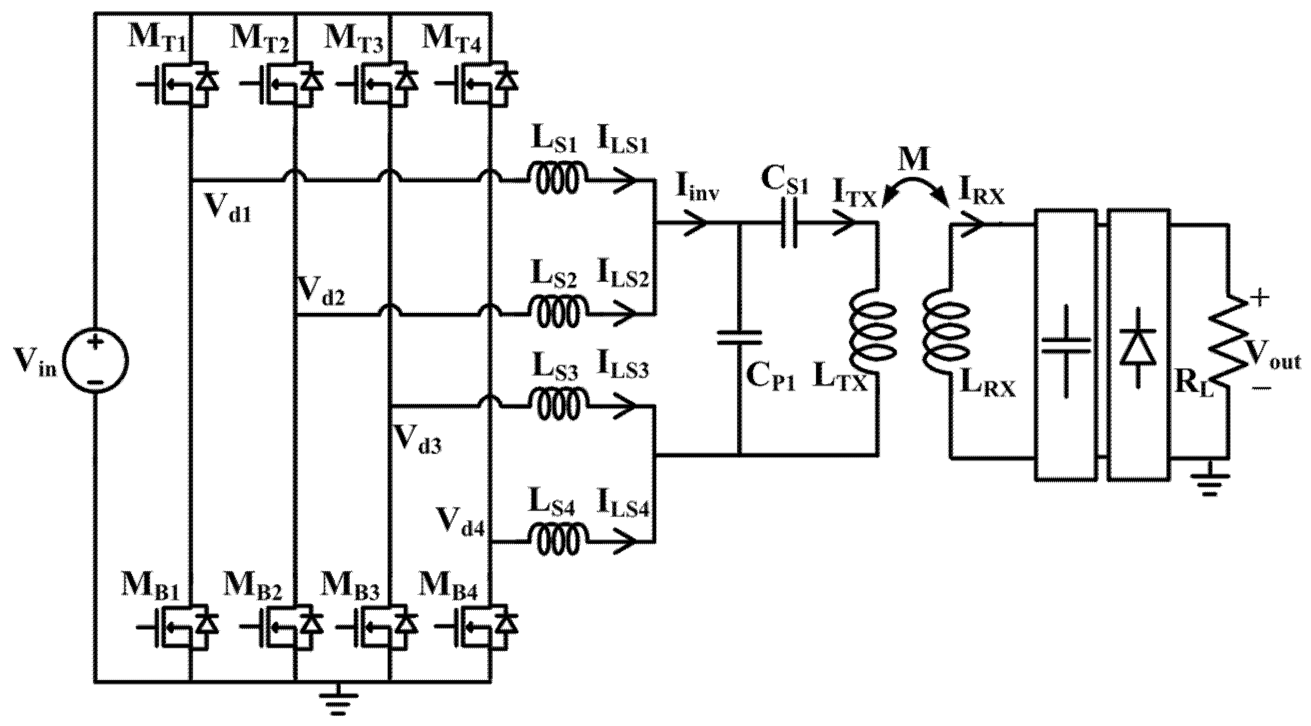
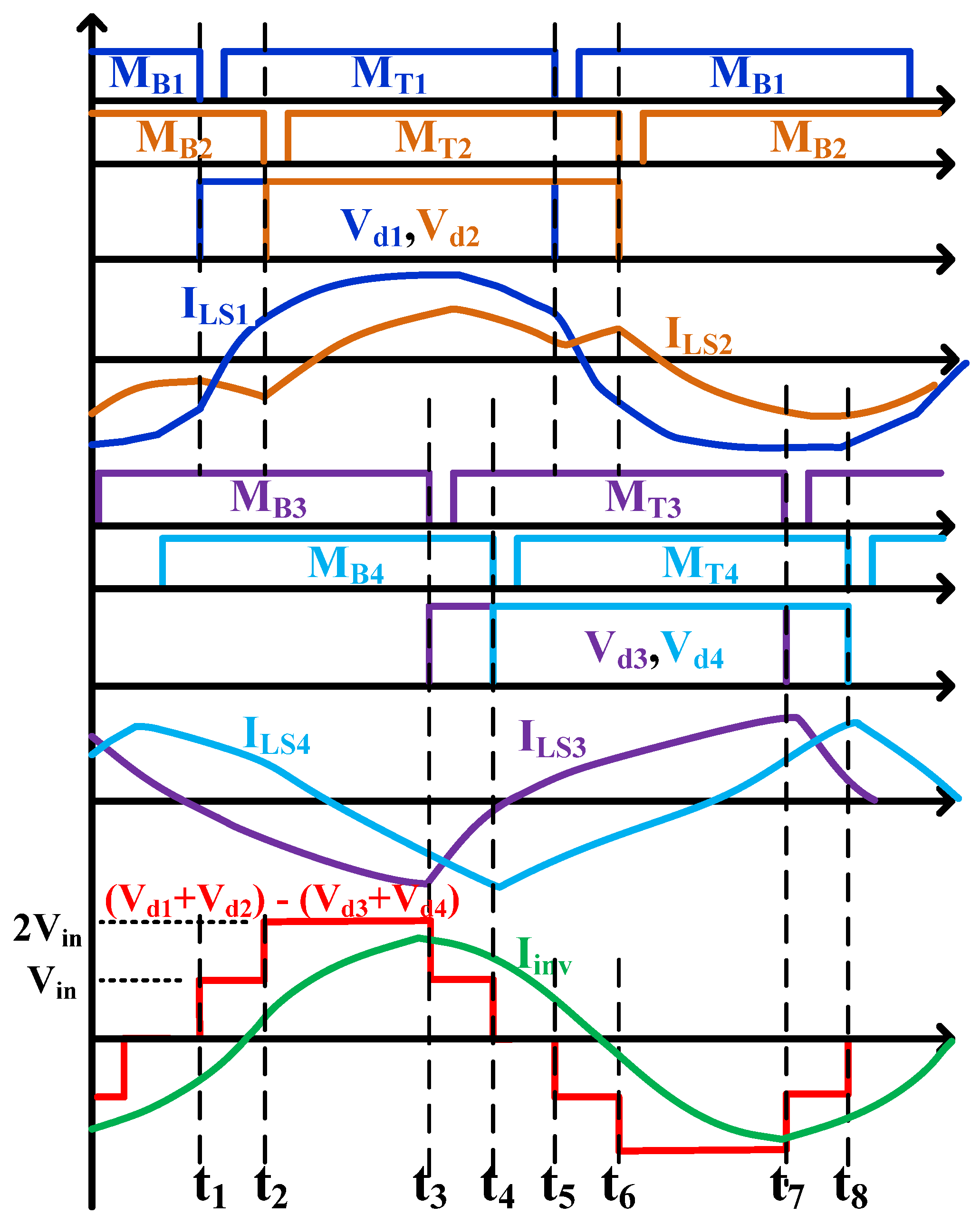
Figure 2 is the proposed multilevel LCC inverter. The inductors LS1 = LS2 = LS3 = LS4 and CP1 are designed to resonate at the switching frequency as in the typical LCC-matching design. Figure 3 illustrates operating waveforms. The output voltages Vd1 and Vd2 have different phases from each other. Even though Vd1 and the Vd2 do not sum in series as in a typical multilevel inverter, the output currents ILS1 due to Vd1 and ILS2 due to Vd2 are summed by two inductors, LS1 and LS2, which form Iinv = ILS1 + ILS2. In the bottommost pane in Figure 3, the summation (Vd1 + Vd2) in the red trace is a conceptual waveform, and it does not physically exist in the circuit. Rather, the physical output is Iinv = ILS1 + ILS2.
Meanwhile, each bridge leg produces its own output voltage and current at different phases. Not only the voltage, but also the current has different phases for each leg. Therefore, each leg achieves ZVS. For example, in Figure 3, at t2, the transition of (Vd1 + Vd2) from Vin to 2Vin occurs when Iinv is positive, or when the phase of Iinv is faster than the second transition of (Vd1 + Vd2) at t2. However, the actual transition at t2 is determined by the turn off of MB2. MB2 and MT2 achieve ZVS because they are switched with their own current ILS2, not with Iinv. In contrast, in the conventional MLI topologies where multiple MOSFETs are series-connected as in Figure 1, there exists only one phase of output current IO for every MOSFET, which causes ZVS failure for some MOSFETs.
The reason why the number of legs is four is that the staircase output in Figure 3 requires eight transitions, and each leg provides two transitions. Referring to Figure 3, the transitions in the red staircase coincide with the falling edge of the leg. Eight transitions require eight switches, which also need four legs. Three or five legs cannot produce the staircase output in Figure 3 because they produce six or ten transitions, respectively. Such waveforms are not symmetrical and worsen the EMI.

3.2. ZVS Switching Sequence

Figure 3 illustrates the switching sequences.
At t1: MB1 turns off, and this determines the rising edge of Vd1. The body diode of MT1 (DT1) begins to conduct before MT1 turns on, and this allows ILS1 to flow in the negative direction, which achieves ZVS.
At t2: MB2 turns off, and Vd2 rises from 0 to positive. At this moment, although the inverter current (Iinv), which is the sum of ILS1 and ILS2, is faster than the second transition in the staircase voltage, the leg output ILS2 is slower than the Vd2. ILS2 can flow in a negative direction, and the body diode of MT2 (DT2) starts conducting before the MT2 channel turns on. This achieves ZVS of MT2, even though Iinv is positive.
At t3: MB3 MOSFET is turned off, and this determines the rising edge of Vd3. The leg output current ILS3 flows in the negative direction, and MT3’s body diode (DT3) begins to conduct before the MT3 channel turns on. This achieves ZVS of MT3.
At t4: MB4 turns off, and MT4’s body diode (DT4) starts conducting before the MT4 channel turns on. Vd4 rises from 0 to a positive voltage, and ILS4 flows in the negative direction, which achieves ZVS of MT4.
The sequence of t5~t8 is similar to t1~t4.
Figure 3. Timing diagram of the proposed multilevel LCC inverter.
Energies 19 01063 g003

3.3. Phase Angle to Reduce Harmonic Distortion

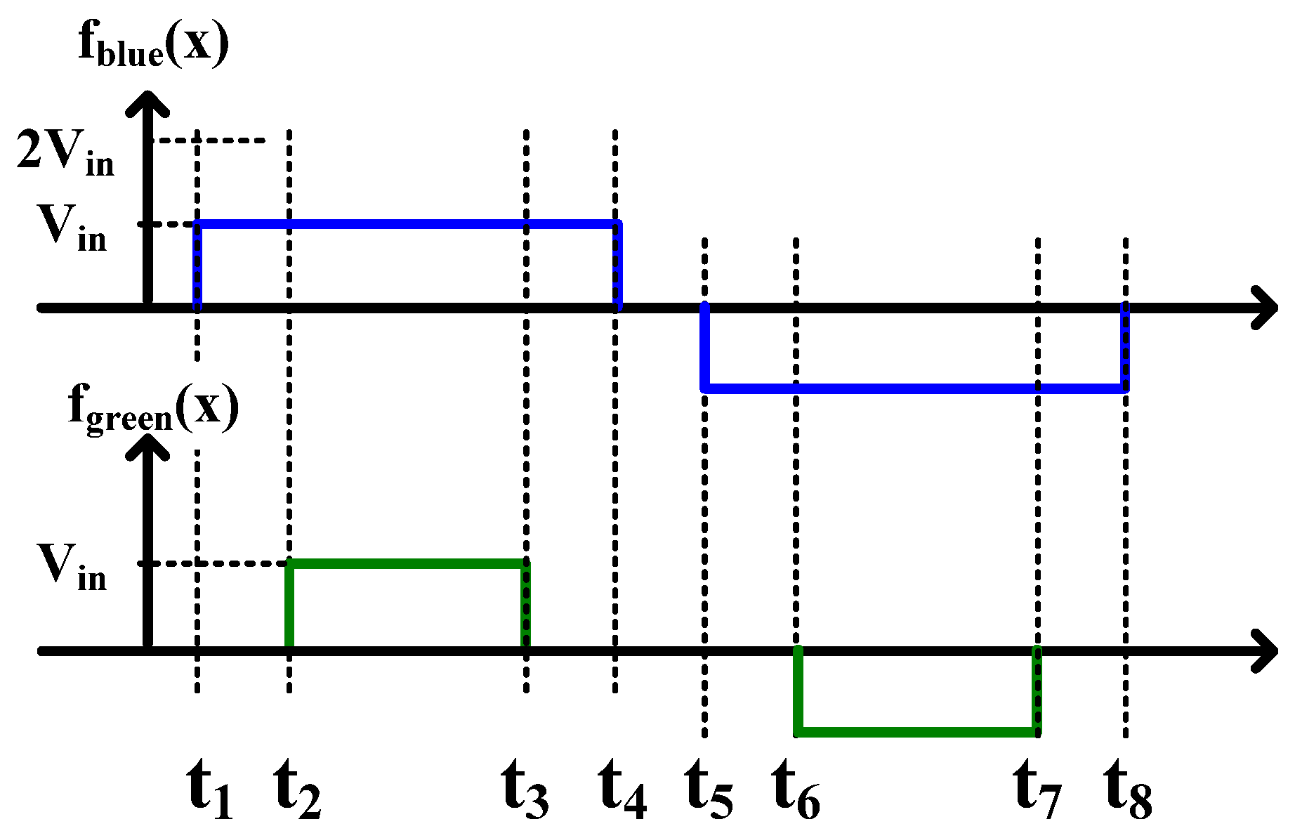
Typically, the third harmonic distortion is the most severe problem because its amplitude is the highest among all harmonics. The next consideration is the fifth harmonic, which usually causes the second-largest distortion. The Fourier series of the red-colored staircase waveform in Figure 3 is calculated as follows. The staircase waveform can be split into two components, as in Figure 4, such that the summation of the blue and green components produces the original staircase waveform in Figure 3. For the blue component, the Fourier series is as follows.
Figure 4. The staircase waveform is split into two parts for Fourier analysis.
Energies 19 01063 g004
b n , b l u e = 1 π 0 2 π f b l u e ( x ) sin n x d x = 1 π t 1 t 4 V i n sin n x d x + 1 π t 5 t 8 ( V i n ) sin n x d x
Now, due to the waveform symmetry, t4 = π − t1, t5 = π + t1, and t8= 2π − t1. Equation (1) becomes
b n , b l u e = V i n n π cos n ( π t 1 ) cos n t 1 + V i n n π cos n ( 2 π t 1 ) cos n ( π + t 1 ) = 4 V i n n π cos n t 1
Similarly, for the green component at t2~t3 and t6~t7, bn,green is
b n , g r e e n = 1 π t 2 t 3 V i n sin n x d x + 1 π t 6 t 7 ( V i n ) sin n x d x = 4 V i n n π cos n t 2
with the symmetry of t3 = π − t2, t6 = π + t2, and t7= 2π − t2. Summing (2) and (3) gives the total Fourier coefficient
b n = 4 V i n n π cos n t 1 + cos n t 2
Now, to suppress the third harmonic (n = 3), b3 should be zero, i.e.,
b 3 = 4 V i n 3 π cos 3 t 1 + cos 3 t 2 = 0
This is achieved when
t 1 + t 2 = π / 3
Meanwhile, the fifth harmonic component should also be zero, i.e.,
b 5 = 4 V i n 5 π cos 5 t 1 + cos 5 t 2 = 0
We want to suppress both the third and fifth harmonics simultaneously. Therefore, substituting (6) into (7) gives
b 5 = 4 V i n 5 π cos 5 t 1 + cos 5 ( π / 3 t 1 ) = 4 V i n 5 π 1.5 cos 5 t 1 0.87 sin 5 t 1 = 0
Equation (8) is satisfied if t1 = 13°. According to (6), t2 is 47°.
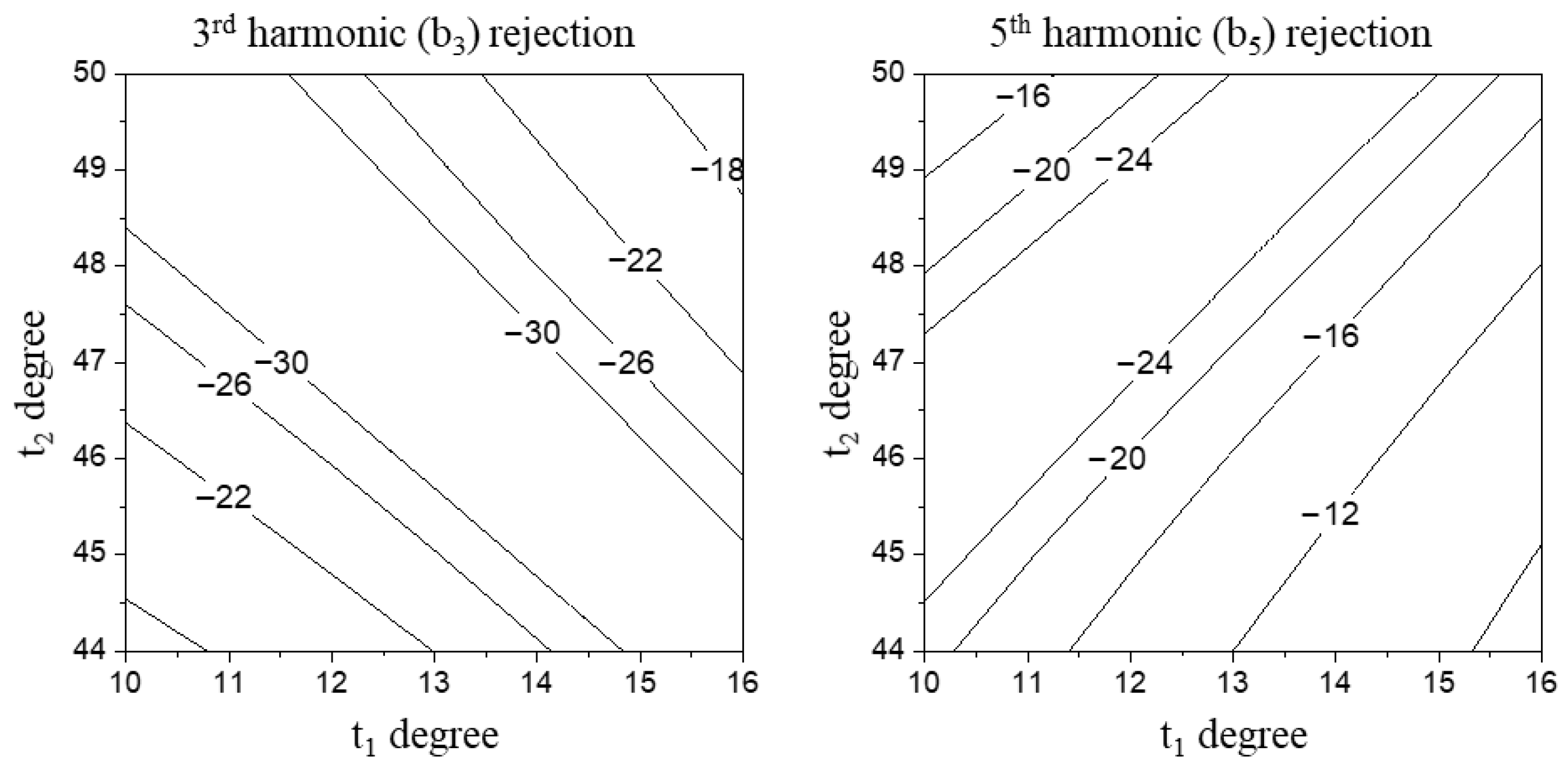
Figure 5 presents the suppression of b3 and b5 when the angles have error deviations. Typical propagation delay variations of a few tens of nanoseconds correspond to 1~2 degrees at 85 kHz. For such typical delay variations, the degradations of suppression are not very severe.

3.4. Discussion on Volume and Harmonic Rejection Performance

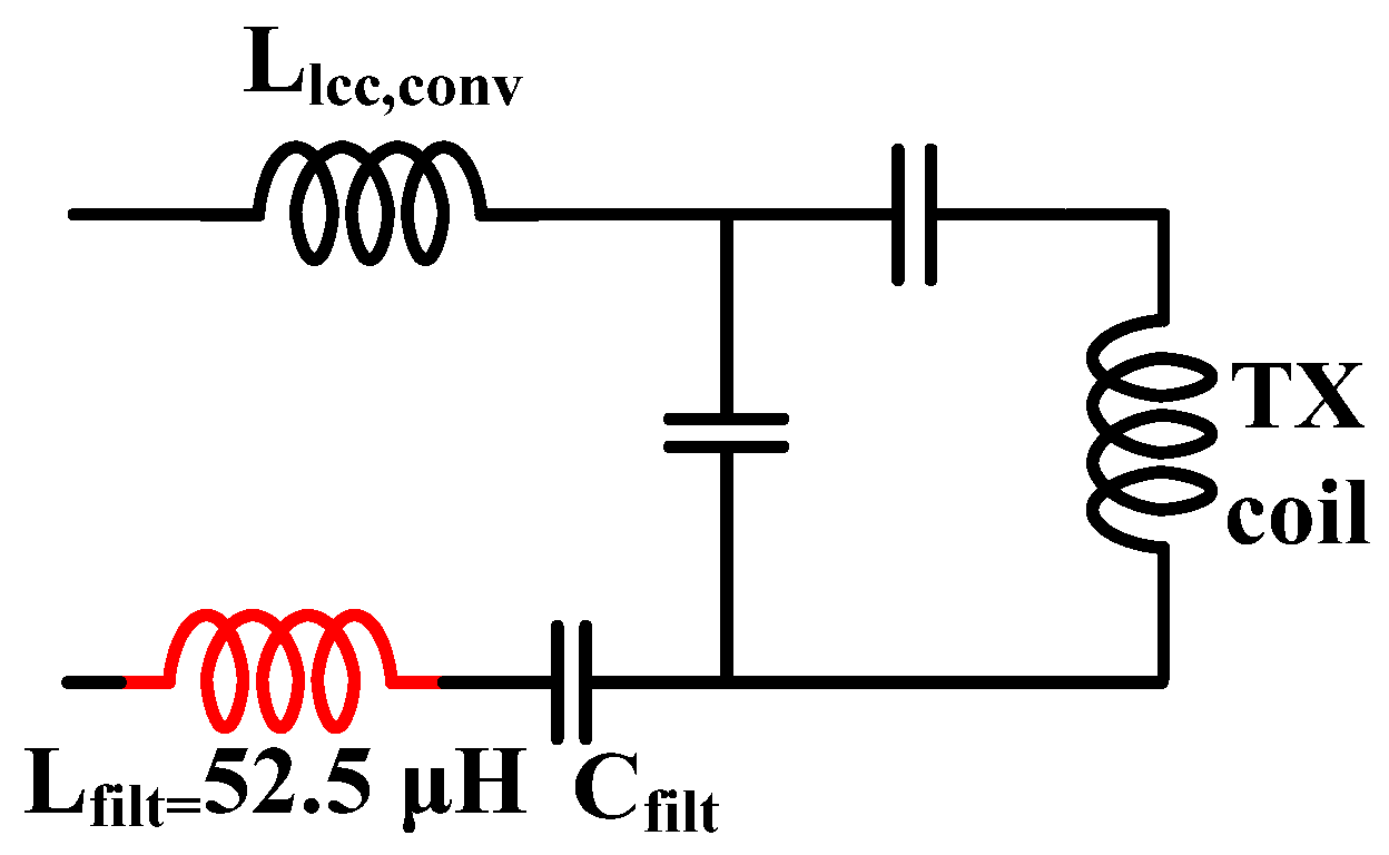
Although the multiple resonant inductors (LS1–LS4) increase size compared to a simple basic inverter, the basic inverter should add a bandpass (inductor–capacitor) filter to remove harmonics at the same branch as in reference [4]’s Figure 14. The performance of the bandpass filter is simulated in Figure 6. The inductance of the bandpass filter for the simple inverter is set to be the same as the summation of additional resonant inductors of the proposed method. In other words, Lfilt is 52.5 μH, which equals LS2 + LS3 + LS4 in order to keep the inductances of the proposed and simple inverter identical to each other. The remainder of the system parameters, such as load and TX-RX coil parameters, are kept the same for the proposed and the simple inverter in Table 2. The third harmonic rejection of ITX output for the proposed and the simple filtering is 17.2 dB and 8.9 dB, respectively. Therefore, to achieve the same harmonic rejection performance, the inductance of the bandpass filter of the simple inverter is larger than that of the proposed method.

3.5. Difference from Prior Current-Interleaved Inverters

The purpose of a typical current-interleaved inverter is to reduce switching frequency ripple (usually 10~100 kHz) in order to produce a clean 60 Hz sinusoid output, i.e., the target sinusoid output frequency is much lower than the switching frequency. In contrast, the proposed inverter’s switching frequency (85 kHz) is equal to the desired output sinusoid because WPT applications require an 85 kHz clean sinusoid output. Most of the WPT applications use resonant inverters, of which the switching frequency (85 kHz) is close to the resonance frequency of the matching network. Hence, the switching frequency is not considered as a ripple or noise. Instead, it is the harmonics of switching frequency that needs to be suppressed.
In this regard, the phase shift for each leg is also different. The proposed inverter’s phases of 13° and 47° do not cancel the 85 kHz switching frequency itself. Instead, it is designed to cancel the harmonics of the switching frequency. On the other hand, a typical interleaved system’s phase is 0°–120°–240° or 0–180° in order to cancel the switching frequency itself. The output matching network and zero-voltage switching are also different. The proposed inverter is for an LCC resonant inverter, and zero-voltage switching (ZVS) is achieved. In contrast, typical low-frequency inverters do not employ resonant topology and ZVS.

4. Experimental Results

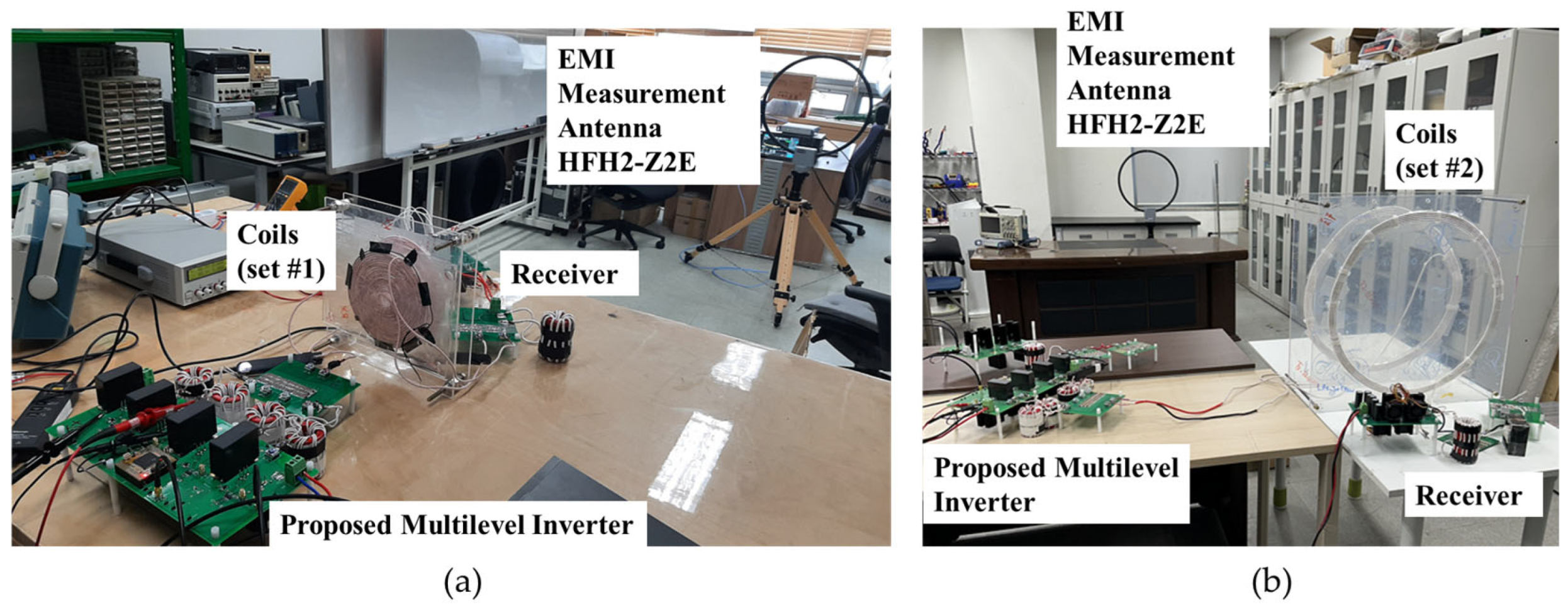
Figure 7 shows the measurement setup for the proposed wireless power transfer system. Two different configurations of TX-RX coils are used to verify the EMI suppression of the proposed inverter. In the first configuration, the diameter of coils is 20 cm, and the distance between the TX and RX coils is 6 cm. In the second configuration, the coil diameter is 51 cm, and the distance between TX and RX varies across 20~36 cm. This is to test the inverter with various operating scenarios. The circuit design parameters and specifications are detailed in Table 2. The proposed circuit operates with a single DC input source of 380 Vin. The switching frequency is 85 kHz, and the load output power is a maximum of 3.4 kW. The TMS320F28335 MCU generates the necessary clocks. Because the proposed inverter does not require any control algorithms, such as capacitor voltage balancing, the MCU just generates fixed clocks.
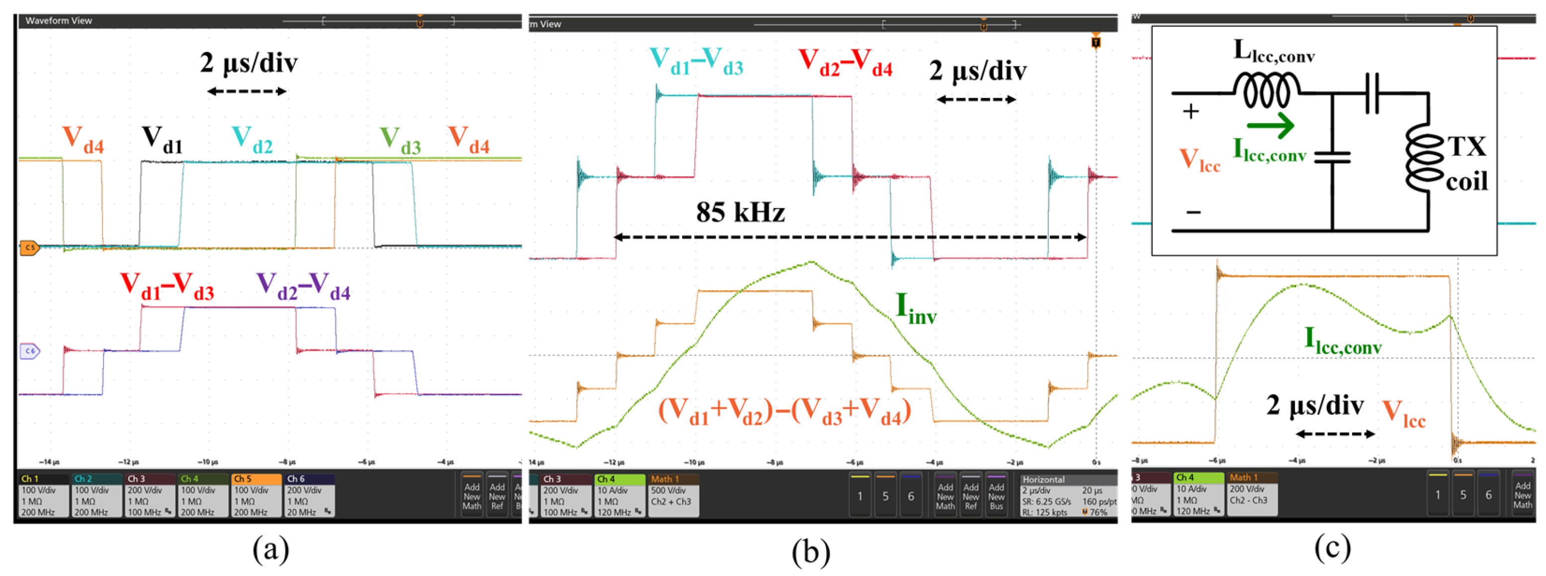
In oscilloscope captures in Figure 8, 100~200 MHz notates the sampling frequency of oscilloscope equipment, which is not related to the switching frequency of 85 kHz.
Figure 8a,b show how the hypothetical multilevel voltage output is produced. Figure 8b also shows that the proposed LCC inverter output, Iinv, becomes nearly sinusoid compared to the conventional LCC output current Ilcc,conv in Figure 8c. Figure 8c shows that the conventional LCC matching output Ilcc,conv contains significant harmonic components.
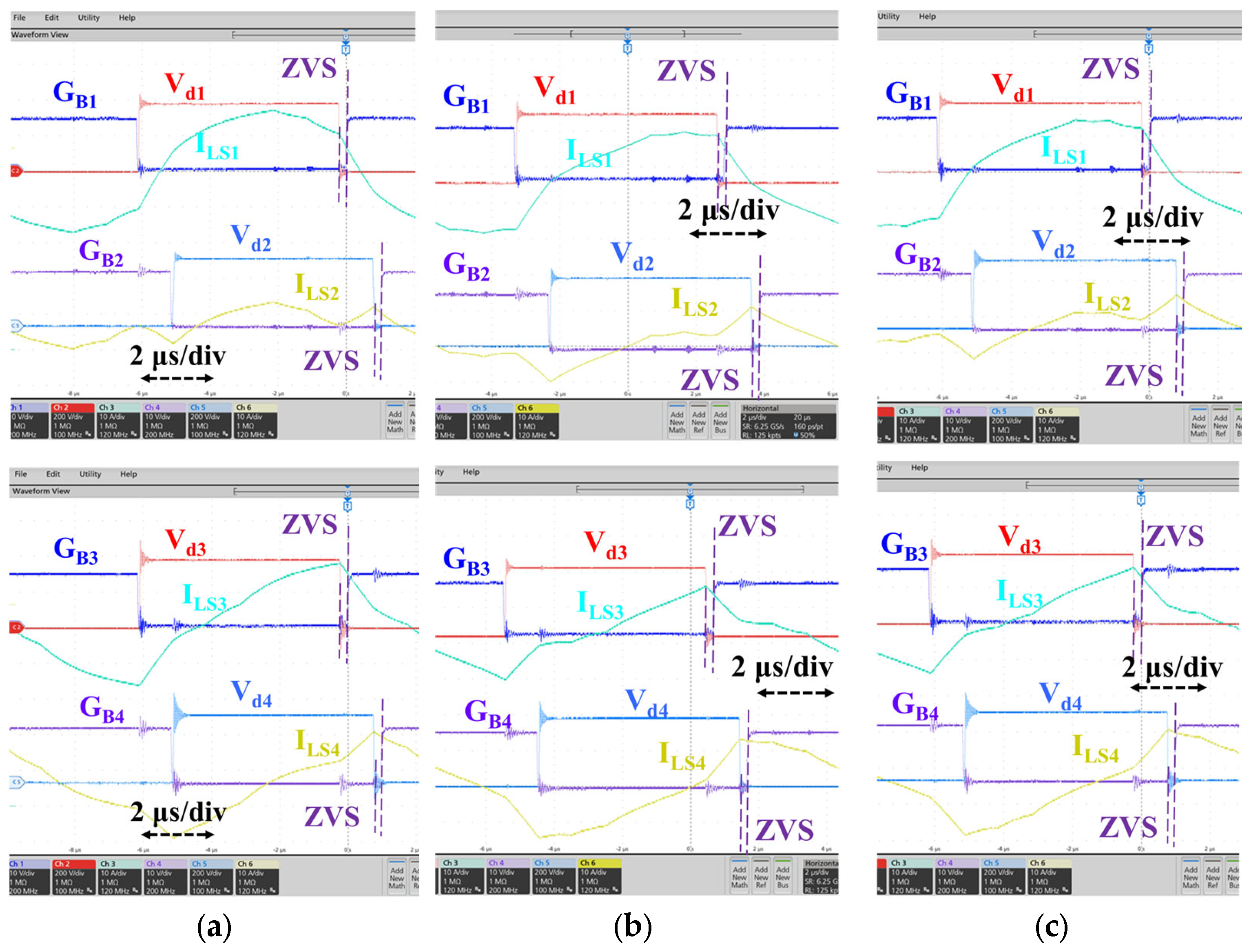
Figure 9 shows that the phase of the individual current for each leg is different, depending on the phase of each leg’s voltage. Each leg’s current is negative at the rising edge of Vdn (n = 1,2,3,4), which enables ZVS for all switches. This is the advantage compared to typical voltage-summing MLIs, as discussed in Section 2. The summation of ILS1 and ILS2 in Figure 9 becomes the final inverter output Iinv in Figure 8b. The summation of ILS3 and ILS4 in Figure 9 is of opposite polarity and the same magnitude as Iinv. Figure 9 also shows the effect of coupling and load variations. For the variations of TX-RX coil distance (i.e., coupling coefficient) and load, ZVS is maintained for all bridge legs.
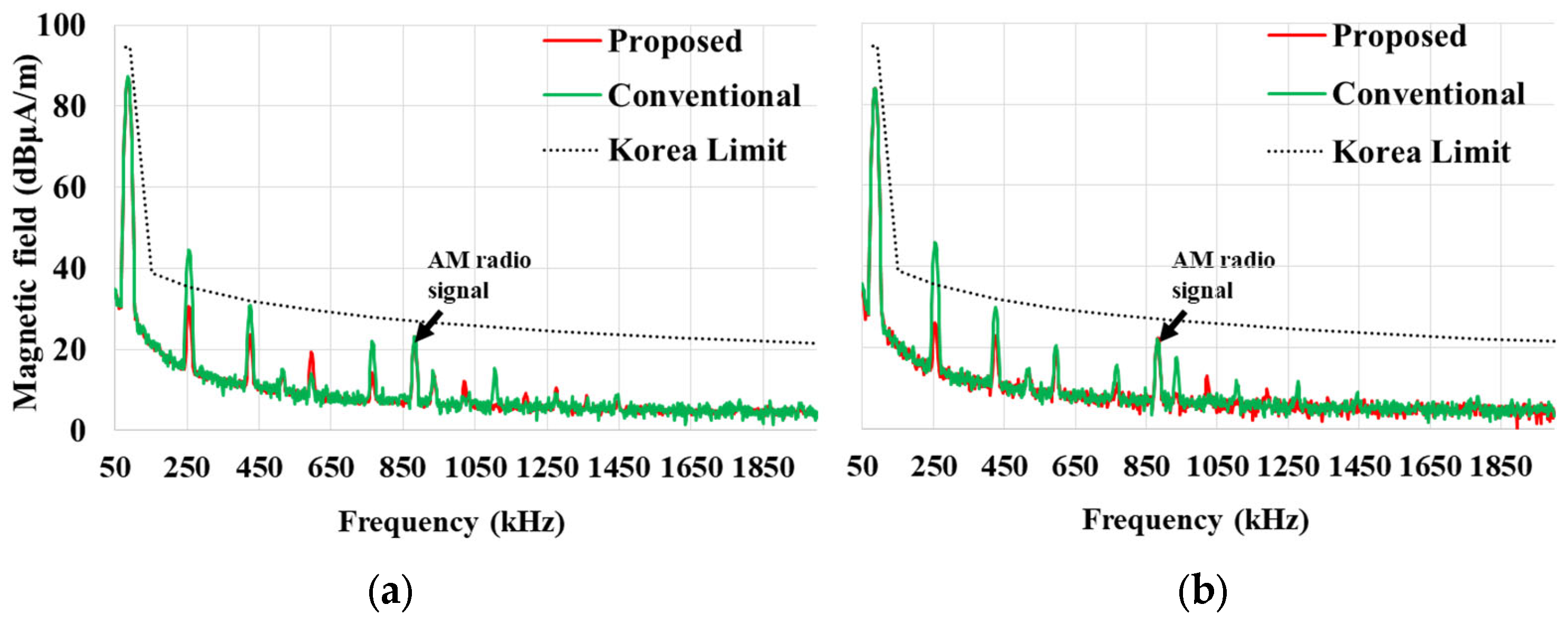
Figure 10 compares the measured radiated EMI harmonics between the proposed multilevel LCC inverter and the conventional LCC inverter. The schematic of conventional LCC is in Figure 8c. The EMI measurement equipment for Figure 10 are N9000B by Keysight and the HFH2-Z2E active loop antenna manufactured by Rohde & Schwarz. The measured noise floor of the N9000B and HFH2-Z2E combination was 14 dBμA/m at 255 kHz, 10 dBμA/m at 425 kHz, and 6 dBμA/m at 1 MHz, as shown in Figure 10, except for the 882 kHz peak of the AM radio broadcasting signal (Korean Broadcasting System corp.), which is not related to the device under test. The antenna is located at a distance of 3 m from the wireless power coils. Figure 7a shows the arrangements. As shown in Figure 10, the proposed multilevel LCC reduced EMI by 14 dB and 7 dB for the third (255 k) and fifth (425 k) harmonics, respectively. It is seen that the EMI suppression performance is maintained for full load conditions and no-load conditions. In contrast, the conventional LCC inverter fails to satisfy the Korea EMI regulation at the third harmonic (255 k) and cannot secure enough of a safety margin for the fifth harmonic (425 k). Additionally, the proposed MLI reduced total harmonic distortion (THD) by 12 dB.
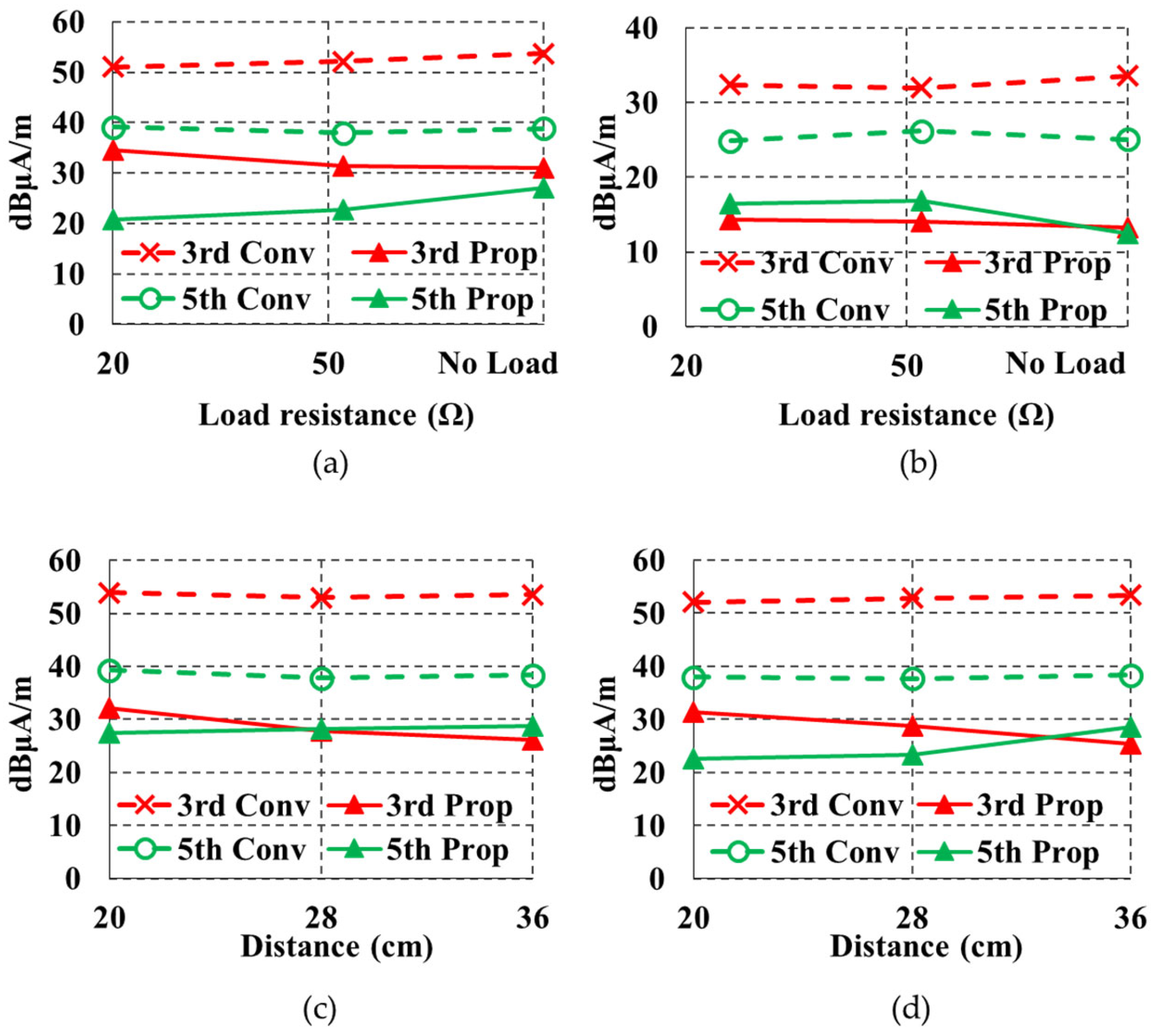
Figure 11 shows the measured EMI harmonic levels for variations of load resistance and TX-RX coil distance. Figure 11 is measured with 51 cm diameter TX and RX coils. Tektronix MDO3024, in spectrum analyzer mode, is used along with the same HFH2-Z2E EMI sensor antenna, of which the noise floor is 5 dBμA/m. Harmonic suppression performance is maintained for load and coupling coefficient variations. Figure 11b is the same load resistance variation as Figure 11a, except that the location of the sensor antenna varies to 7 m.
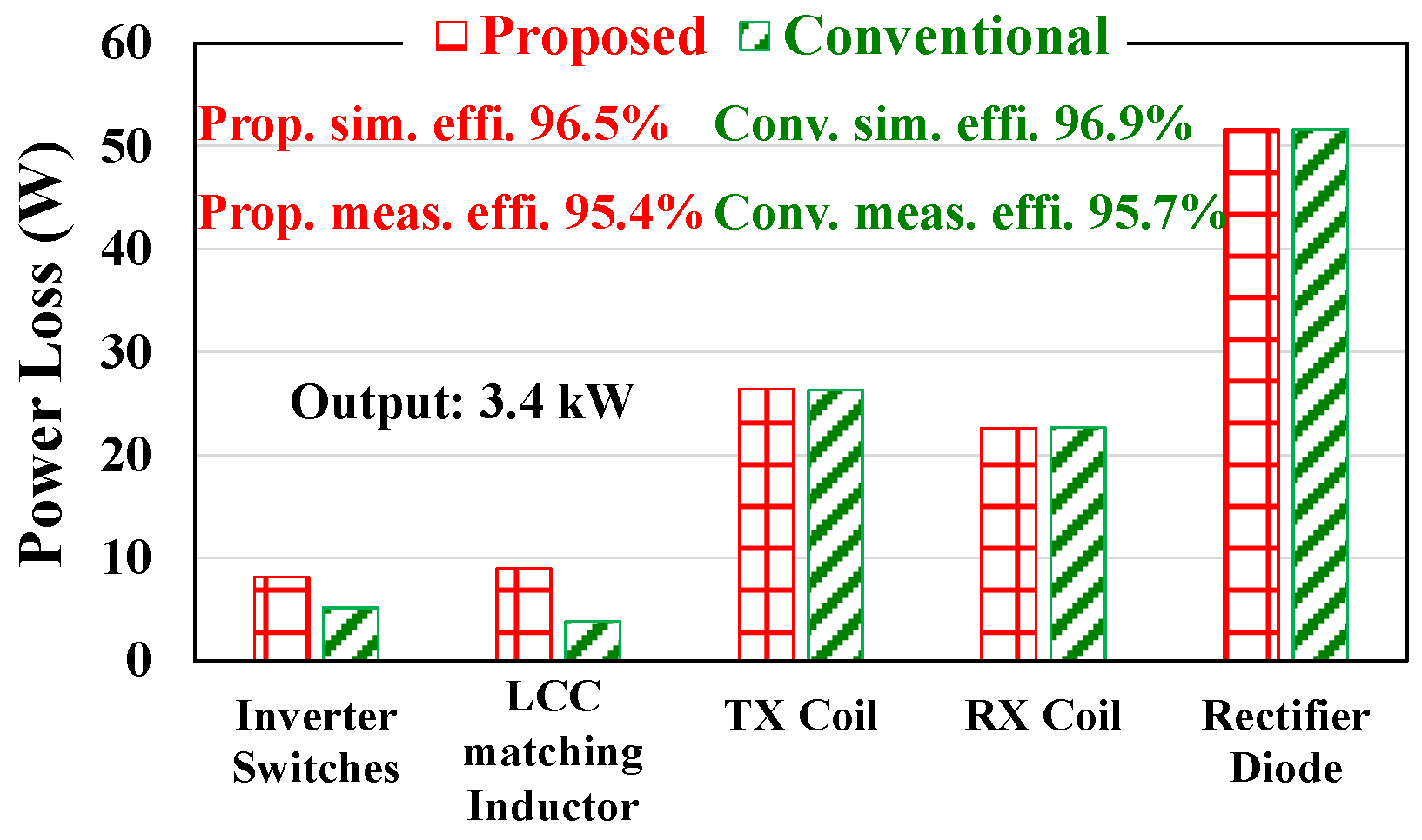
Figure 12 compares the power loss. The overall efficiency is measured from the 380V DC input source to the DC output load. Although the proposed method slightly reduces the overall efficiency by 0.3%, the harmonic distortion became lower, and the Korean EMI regulation can be satisfied.
Table 3 compares prior multilevel inverters for wireless power transfer applications. The proposed method achieves high efficiency and ZVS with the low-distortion staircase output. These are obtained using a single DC input source, and capacitor voltage balancing is not necessary.

5. Conclusions

This paper proposes a multilevel LCC inverter for wireless power transfer applications in order to suppress harmonic distortions and radiated EMI. Unlike conventional multilevel inverters, the proposed method achieves ZVS while outputting a sinusoid-mimicking staircase waveform. Moreover, the method uses only a single DC input source, and capacitor voltage balancing is not necessary. The proposed inverter suppresses the third harmonic EMI by 14 dB and the fifth harmonic by 7 dB. The system is running in an open loop without feedback control. However, it is seen that ZVS and harmonic suppression are not affected by coupling and load variations.

Author Contributions

Conceptualization, D.A.; methodology, W.H.K.; validation, W.H.K.; formal analysis, D.A.; investigation, W.H.K.; data curation, W.H.K.; writing—original draft preparation, D.A.; writing—review and editing, W.H.K.; visualization, W.H.K.; supervision, D.A.; funding acquisition, D.A. All authors have read and agreed to the published version of the manuscript.

Funding

This research was funded by Incheon National University, grant number 2021-0429, and the APC was funded by Incheon National University.

Data Availability Statement

The original contributions presented in this study are included in the article. Further inquiries can be directed to the corresponding author.

Conflicts of Interest

The authors declare no conflict of interest.

References

  1. Government of Korea. Electromagnetic Compatibility Law. June 2023. Available online: https://law.go.kr/LSW/admRulLsInfoP.do?admRulId=2090549&efYd=0#AJAX (accessed on 1 July 2025).
  2. Sim, B.; Jeong, S.; Kim, Y.; Park, S.; Lee, S.; Hong, S.; Song, J.; Kim, H.; Kang, H.; Park, H.; et al. A Near Field Analytical Model for EMI Reduction and Efficiency Enhancement Using an nth Harmonic Frequency Shielding Coil in a Loosely Coupled Automotive WPT System. IEEE Trans. Electromagn. Compat. 2021, 63, 935–946. [Google Scholar] [CrossRef]
  3. Maradei, F.; Ahn, S.; Campi, T.; Covic, G.; Cruciani, S.; Hirata, A.; Wang, S.; Feliziani, M. EMC and EMF Safety Aspects of Wireless Power Transfer Systems for e-Mobility. IEEE Electromagn. Compat. Mag. 2024, 13, 74–92. [Google Scholar] [CrossRef]
  4. Woo, S.; Shin, Y.; Rhee, J.; Huh, S.; Ahn, S. Design of Resonant Circuit Components to Suppress both EMF and EMI in Wireless Power Transfer Systems for Electric Vehicles. IEEE J. Emerg. Sel. Top. Power Electron. 2025; early access. [Google Scholar] [CrossRef]
  5. Hu, J.; Zhao, J. Design of wireless power transfer system with input filter. IET Power Electron. 2020, 13, 1393–1402. [Google Scholar] [CrossRef]
  6. Kim, H.; Song, C.; Kim, D.-H.; Kim, J. Design of conductive shield for wireless power transfer system for electric vehicle considering automotive body. In Proceedings of the IEEE International Symposium on Electromagnetic Compatibility (EMC), Dresden, Germany, 16–22 August 2015; pp. 1369–1374. [Google Scholar]
  7. Jeong, S.; Kim, D.-H.; Song, J.; Kim, H.; Lee, S.; Song, C.; Lee, J.L.; Song, J.; Kim, J. Smartwatch Strap Wireless Power Transfer System with Flexible PCB Coil and Shielding Material. IEEE Trans. Ind. Electron. 2019, 66, 4054–4064. [Google Scholar] [CrossRef]
  8. Woo, S.; Shin, Y.; Lee, C.; Moon, J.; Kim, H.; Kim, H.; Huh, S.; Ahn, S. Design and Analysis of LCC-S Wireless Power Transfer Systems Considering Load-Dependent Leakage Magnetic Field. IEEE Trans. Electromagn. Compat. 2024, 66, 1015–1028. [Google Scholar] [CrossRef]
  9. Guo, J.; Chau, K.T.; Liu, W.; Hua, Z.; Li, S. Segmented-Vector Pulse Frequency Modulated Three-Level Converter for Wireless Power Transfer. IEEE Trans. Power Electron. 2024, 39, 8959–8972. [Google Scholar] [CrossRef]
  10. Lee, J.-Y.; Liao, C.-Y.; Yin, S.-Y.; Lo, K.-Y. A Multilevel Inverter for Contactless Power Transfer System. IEEE Trans. Circuits Syst. II Express Briefs 2021, 68, 401–405. [Google Scholar] [CrossRef]
  11. Nguyen, B.X.; Vilathgamuwa, D.M.; Foo, G.; Wang, P.; Ong, A. A modified cascaded multilevel converter topology for high power bidirectional inductive power transfer systems with the reduction of switching devices and power losses. In Proceedings of the IEEE 11st International Conference on Power Electronics and Drive Systems, Surathkal, India, 18–21 December 2015; pp. 93–97. [Google Scholar]
  12. Liu, Y.; Liu, C.; Gao, X.; Liu, S. Design and Control of a Decoupled Multichannel Wireless Power Transfer System Based on Multilevel Inverters. IEEE Trans. Power Electron. 2022, 37, 10045–10060. [Google Scholar] [CrossRef]
  13. Zade, A.; Teeneti, C.R.; Mansour, M.; Gurudiwan, S.; Hesterman, B.; Wang, H.; Zane, R. A 21-kW Unfolding-Based Single-Stage AC–DC Converter for Wireless Charging Applications. IEEE J. Emerg. Sel. Top. Power Electron. 2024, 12, 8–27. [Google Scholar] [CrossRef]
  14. Ge, X.; Wang, Y.; Tang, M.; Wang, L. A Power Boosting Method for Wireless Power Transfer Systems Based on a Multilevel Inverter and Dual-Resonant Network. Electronics 2024, 13, 4066. [Google Scholar] [CrossRef]
  15. Manivelan, C. A Survey on Multilevel Inverter Topologies and Control Schemes with Harmonic Elimination. In Proceedings of the International Conference on Electrotechnical Complexes and Systems (ICOECS), Ufa, Russia, 27–30 October 2020; pp. 1–7. [Google Scholar]
  16. Rahnamaee, H.R.; Thrimawithana, D.J.; Madawala, U.K. MOSFET based Multilevel converter for IPT systems. In Proceedings of the IEEE International Conference on Industrial Technology ICIT, Busan, Republic of Korea, 26 February–1 March 2014; pp. 295–300. [Google Scholar]
  17. Guo, J.; Chau, K.T.; Liu, W.; Hou, Y.; Chan, W.L. Pulse Magnitude Modulation and Token Rotation-Based Voltage Balancing Method of Multilevel Inverter for Wireless Power Transfer. IEEE Trans. Power Electron. 2025, 40, 4652–4663. [Google Scholar]
  18. Wang, W.; Thrimawithana, D.; Neuburger, M. An Si MOSFET-Based High-Power Wireless EV Charger With a Wide ZVS Operating Range. IEEE Trans. Power Electron. 2021, 36, 11163–11173. [Google Scholar] [CrossRef]
  19. Wang, W.V.; Thrimawithana, D.J.; Lin, F.; Covic, G.A. An MMC-Based IPT System with Integrated Magnetics and ZVS Operations. IEEE Trans. Power Electron. 2022, 37, 2425–2436. [Google Scholar] [CrossRef]
Figure 1. Issues of typical multilevel inverters for WPT application. (a) ZVS failure issue when the staircase output is generated. ZVS failure occurs at the transition from S4 ON to S1 ON. Diode reverse recovery also occurs at S4 off. (b) Voltage imbalance issue. The Cfly voltage cannot be set at exactly half of the DC input voltage, thereby distorting the output voltage waveform.
Energies 19 01063 g001
Figure 2. Proposed multilevel LCC inverter for WPT.
Energies 19 01063 g002
Figure 5. Sensitivity of EMI rejection performance due to variations from ideal angles.
Energies 19 01063 g005
Figure 6. A simple inverter with a bandpass filter with equal total inductances. The harmonic rejection of the simple filter is only 8.9 dB, which is lower than the 17.2 dB of the proposed MLI. The remainder of the parameters are shown in Table 2.
Energies 19 01063 g006
Figure 7. Measurement setup. The same inverter board is used for different types of coils. (a) With 20 cm diameter coils. (b) With 51 cm diameter coils.
Energies 19 01063 g007
Figure 8. (a) Vd1, Vd2, Vd3, and Vd4 voltages of the proposed LCC inverter. (b) Staircase multilevel voltage and near-sinusoid output current of the proposed multilevel LCC inverter. (c) Conventional LCC inverter with the same TX and RX coils being used. The Ilcc,conv output contains significant harmonic distortions, which are typical characteristics of the LCC matching network. The inset notates conventional LCC schematics with voltage and current symbols.
Energies 19 01063 g008
Figure 9. ZVS for each leg. GB1~GB4 are gate-driving signals of MB1~MB4, respectively. ZVS is achieved for the variations of TX-RX coil distance (which varies the coupling coefficient) and load resistance (GBn: 10 V/div, Vdn: 200 V/div, ILSn: 10 A/div, where n = 1, 2, 3, 4 is iteration index). (a) TX-RX coil distance of 5 cm and load resistance of 11 Ω. (b) TX-RX coil distance of 10 cm and load resistance of 11 Ω. (c) TX-RX coil distance of 5 cm and load resistance of 5 Ω.
Energies 19 01063 g009
Figure 10. Measured radiated EMI. With 20 cm diameter TX and RX coils. The proposed method suppresses harmonics in order to satisfy the Korean government regulation [1]. (a) At full load condition. (b) Receiver load is disconnected (no load).
Energies 19 01063 g010
Figure 11. Measured third and fifth EMI harmonics for variations of load and TX-RX coil distances. With 51 cm diameter TX and RX coils. Except for (b), the EMI sensor antenna is placed at a 5 m distance. (a) Load variation. (b) Load variation, with the EMI sensor antenna location being varied to 7 m. (c) TX-RX distance variations with 26 Ω load. (d) TX-RX distance variations with 52 Ω load.
Energies 19 01063 g011
Figure 12. Power loss analysis with the proposed MLI LCC and the conventional LCC at a 3.4 kW load output condition.
Energies 19 01063 g012
Table 1. Comparison of multilevel inverters.
TypeStaircase Output GenerationObviating Capacitor Voltage Balancing ControlSingle DC Source Operation
FCOXO
NPCOXO
Series-stackedOOX
ModularXXO
ProposedOOO
Table 2. Circuit design parameters and specifications.
ParameterValueParameterValue
LTX (set#1)
LTX (set#2)
32.4 µH
32.2 µH
Coil air gap (set#1)
Coil air gap (set#2)
6 cm
20~36 cm
LS1, LS2, LS3, LS417.5 µHfS85 kHz
CS1165 nFVin380 V
CP1198 nFMax Pout3.4 kW
LRX (set#1)32.5 µHLRX (set#2)30.6 µH
Table 3. Comparison with previous multilevel inverters for wireless power.
Topologies[9][10][11][12][13][16][17][19]Proposed
Single-Input Voltage SourceOXXOOXOOO
Staircase Output
Availability
XOOOOOXXO
ZVS For Staircase Outputn/an/aXXXXn/an/aO
Obviating Capacitor
Voltage Balancing
XOn/aXXOXXO
Output Power (W)40050040 k1 k21 k20 k8507.7 k3.4 k
Efficiency95.2%85%n/a (Simul.)84.1%95.96%
(ac-dc)
88%
(Simul.)
92%93%95.4%
Disclaimer/Publisher’s Note: The statements, opinions and data contained in all publications are solely those of the individual author(s) and contributor(s) and not of MDPI and/or the editor(s). MDPI and/or the editor(s) disclaim responsibility for any injury to people or property resulting from any ideas, methods, instructions or products referred to in the content.