1. Introduction
The CHB converter achieves high-voltage output by connecting multiple low-voltage power cells in series. Owing to its modularity, ready scalability, and high output waveform quality, it has found application in medium-voltage variable-speed drives, static synchronous compensators (STATCOMs), and grid-connected photovoltaic inverters [
1,
2,
3,
4,
5,
6]. In high-voltage variable-frequency soft starters, up to 12 power cells are cascaded per phase, and by activating 5 to 12 cascaded layers according to the voltage rating, the application range from 6 kV to 13.8 kV can be covered.
Unipolar frequency-doubling CPS-SPWM is a control strategy widely adopted for CHB converters [
7,
8,
9]. The strategy maintains uniformly spaced carrier phase offsets among the
N cells within each phase. Since a single H-bridge cell already produces two voltage-level transitions per carrier period under unipolar frequency-doubling modulation, the optimal phase-shift increment is Δ
φc = 180°/
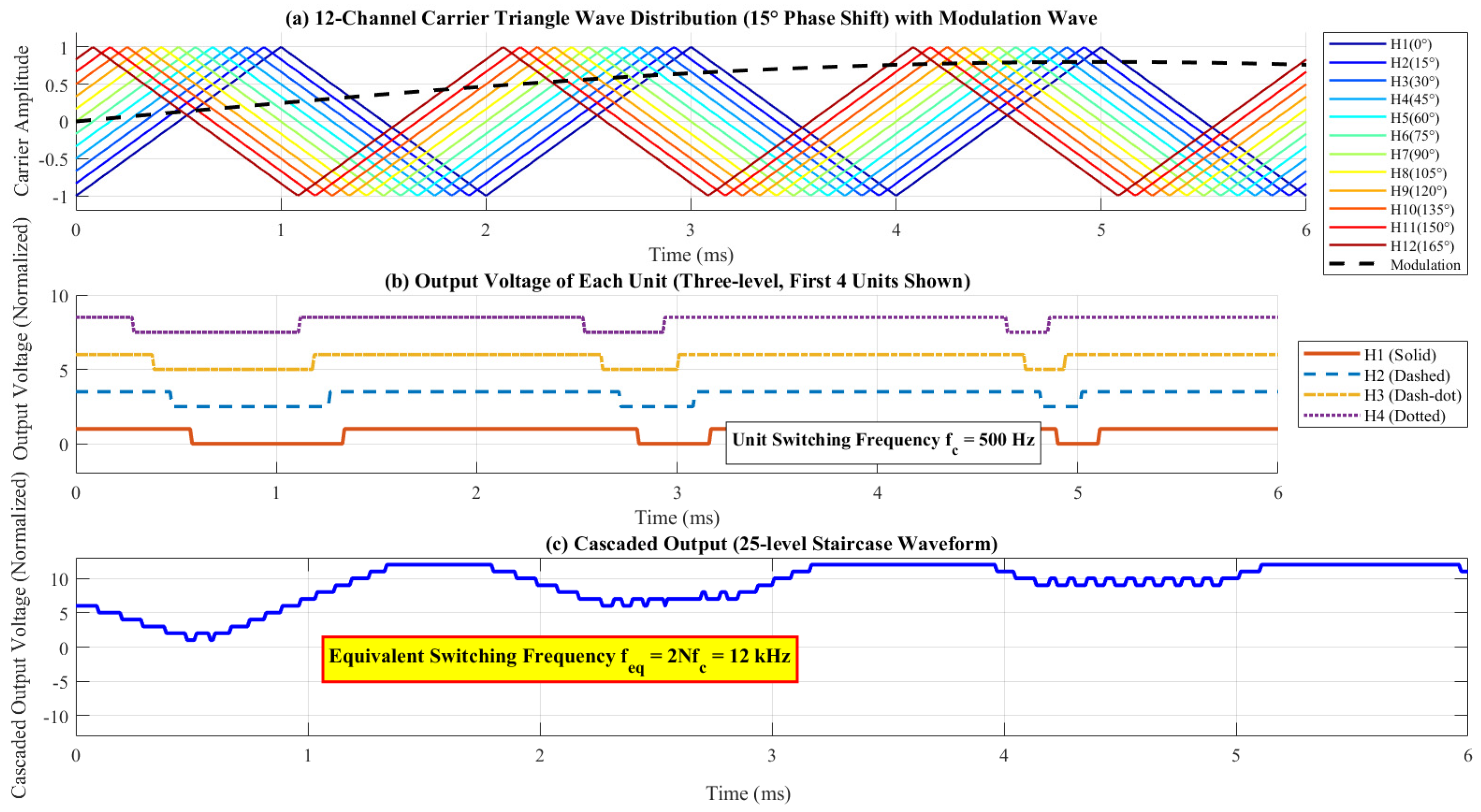
N, which equals 15° for a 12-cell system. After superposition of the individual cell outputs, the dominant ripple frequency is raised from the carrier frequency
fc of a single cell to an equivalent ripple frequency
feq = 2
Nfc. For
N = 12 and
fc = 500 Hz,
feq = 12 kHz, that is, the switching frequency of each IGBT is only 500 Hz while the equivalent switching frequency of the cascaded output reaches 12 kHz, which reduces both switching losses and the output filter volume without compromising output waveform quality [
10,
11].
The above properties of CPS-SPWM presuppose that the carriers of all cells maintain strictly uniform phase offsets. When the phase offsets deviate from their ideal values, the carrier-frequency components and their sidebands, which are intended to cancel one another among the cell outputs, no longer cancel completely, and residual harmonics appear in the vicinity of the carrier frequency in the cascaded output, degrading the output waveform quality [
9,
12,
13,
14]. References [
15,
16] present theoretical, simulation, and experimental analyses of carrier phase-shift modulation for CHB and modular multilevel converter (MMC) systems, respectively. The results indicate that the carrier phase-shift angle directly affects the phasor superposition relationship of the switching harmonics in each power module; when the phase-shift angle deviates from a value conducive to harmonic cancelation, the residual carrier sideband harmonics increase, and the output voltage quality consequently deteriorates.
For a system with fc = 500 Hz (Tc = 2 ms) and Δφc = 15°, the theoretical phase-shift interval between adjacent cells is 83.333 μs. If the synchronization time error between cells is Δtsync, the corresponding equivalent carrier phase error is Δφerr = 360 fc Δtsync.
As shown by the analysis in
Section 2.2, a carrier-phase error prevents exact phasor cancelation of the carrier groups.
Table 1 reports a conservative upper bound for the normalized residual amplitude of the second canceled carrier group. At Δt
sync = 5 μs, the equivalent phase error is 0.90° and the bound is −30.1 dB; at 10 μs, the phase error is 1.80° and the bound rises to −24.0 dB. The 5 μs criterion is therefore treated as a conservative design limit rather than an empirically optimized threshold.
For a 13.8 kV high-voltage soft starter comprising 36 power cells (12 per phase), the carrier synchronization scheme must be realized under the following engineering constraints. First, the cabinet wiring space and the number of wall bushings are limited, so the numbers of optical fibers and transceiver modules on the cell side should be kept as small as possible. Second, all power cells are programmed with an identical firmware image and are assigned no communication address, so as to permit arbitrary interchange of cell positions and the use of common spare parts. Third, dynamic activation of 5 to 12 cascaded layers according to the voltage rating must be supported. Fourth, the scheme should be realizable on the already finalized power cell hardware through minimal modification, without redesign of the printed circuit board, so that installed equipment can be upgraded.
Several approaches to inter-cell time synchronization have been reported in the distributed control of MMC systems. In centralized PWM generation, the master controller directly produces all gate drive signals within a single clock domain, so that no inter-cell synchronization error exists; however, 144 drive signals are required for 36 cells, and the insulation design on the high-voltage side together with signal integrity becomes difficult, which restricts this approach to small-scale systems of 3 to 5 cells [
17]. The independent synchronization pulse line scheme provides each cell with a data fiber and a dedicated SYNC fiber, and each cell resets its local timer on the SYNC edge, achieving nanosecond-level accuracy at the cost of 72 fibers and 72 optical transceivers for 36 cells, which conflicts with the fiber count constraint of the present application [
18]. In the field of industrial networks, the IEEE 1588 precision time protocol and the Ether CAT distributed clock achieve node synchronization by conveying timing information over the communication link; among the associated techniques, hardware time stamping latches the instant of the message edge directly at the physical layer, thereby avoiding the software jitter introduced by the protocol stack and interrupt handling, and can improve the synchronization accuracy to the sub-microsecond level [
19,
20,
21,
22]. These protocols, however, rely on bidirectional message exchange, node addressing, and a communication controller with timestamping support, whereas the link addressed in this paper is a unidirectional broadcast link built on low-cost plastic optical fiber transceivers with cells carrying no communication address, so that neither the protocol nor the hardware overhead can be accommodated. Against this background, engineering implementations commonly adopt frame-header external-interrupt synchronization, in which the start edge of the data frame serves as the common time reference, a general-purpose input/output (GPIO) external interrupt (EXTI) is triggered, and the timer count value is read in software to compute the phase error. This approach adds no optical fiber and is inexpensive, but the interrupt-response time is affected by the instruction being executed, interrupt priority preemption, and nesting, so that the jitter may reach the microsecond level [
23]. Dedicated synchronization protocol symbols insert synchronization frames or characters into the data stream, and each cell performs phase alignment upon recognition; the identification is more explicit than a frame header, yet the method remains limited by software recognition latency and consumes communication bandwidth [
24]. Fully distributed digital phase locking dispenses with a hard synchronization signal and converges slowly by means of a digital phase-locked loop acting on long-term error statistics; its disturbance immunity is strong, but the initial convergence time may reach tens of seconds, which fails to meet the rapid start-up requirement of soft starters [
25]. A comparison of the conventional synchronization methods is presented in
Table 2.
The progression of inter-cell synchronization has moved from centralized gating and dedicated point-to-point pulses to communication-link reuse, hardware timestamping, and distributed carrier-phase estimation. Recent electrical-variable-based methods [
26,
27] avoid a dedicated timing conductor, but they require current or voltage feedback, iterative phase estimation, and a convergence interval. Hardware-timestamped network methods provide higher accuracy, but normally require bidirectional exchange, node identities, timestamp-capable interfaces, and a clock-servo stack [
19,
20,
21,
22]. These approaches improve either accuracy or wiring efficiency, but none simultaneously provide a unidirectional broadcast link, address-free interchangeable CHB cells, one-cycle hard alignment, and no dedicated synchronization fiber. The contribution of this study is therefore the application-specific combination of frame-edge multiplexing, peripheral-level input capture, and hard/soft alignment. The evidence-controlled comparison in
Table 1 reports synchronization accuracy, hardware and fiber requirements, establishment time, scalability, and per-cell computational burden without treating literature values as same-platform measurements.
Positioning relative to the state of the art is therefore important. The present contribution is not a new generic time-synchronization protocol, nor does it claim accuracy superior to dedicated SYNC fibers or hardware-timestamped bidirectional networks. Its novelty is the application-specific co-design of four functions that are usually treated separately: (i) reuse of the existing one-way downlink frame edge as the timing reference without node addressing or a second fiber; (ii) peripheral-level timer input capture so that CPU interrupt-response latency is removed from the timestamp path; (iii) one-cycle standstill hard alignment followed by rate-limited on-line correction; and (iv) preservation of identical, address-free cell firmware and cell interchangeability. This combination directly targets CHB installations in which wiring density, retrofit constraints, and deterministic microsecond-level synchronization are more important than sub-microsecond network time transfer.
Table 2 reveals a clear trade-off between synchronization accuracy and link cost in the existing methods: those satisfying the fiber count constraint are limited by software latency and offer indeterminate accuracy, whereas those attaining high accuracy either require a doubled fiber resource or presuppose bidirectional protocol support that the present link does not provide. The problem addressed in this paper is therefore how to raise the synchronization accuracy to a level meeting the harmonic cancelation requirement of CPS-SPWM under the conditions of a unidirectional low-cost link, cells without addresses, and minimal hardware modification.
To this end, this paper proposes a carrier synchronization method for CHB CPS-SPWM power cells based on multiplexing the communication data link with the synchronization reference. The work comprises four aspects.
At the analytical level, the switching-function coefficient of each canceled carrier group is factorized into a modulation-dependent term and an inter-cell phase-sum term. This yields an exact residual expression and a small-angle approximation whose error is quantified over carrier-phase errors from 0.18° to 15°. The same factorization supplies a generalized design procedure in which the allowable synchronization error depends on the number of cells N, carrier frequency fc, modulation index M through the selected harmonic coefficient, and the permitted residual-harmonic limit. The 5 μs value is recovered only as the design point for N = 12, fc = 500 Hz, M within the linear modulation range, and a −30.1 dB residual bound; it is not asserted as a universal threshold.
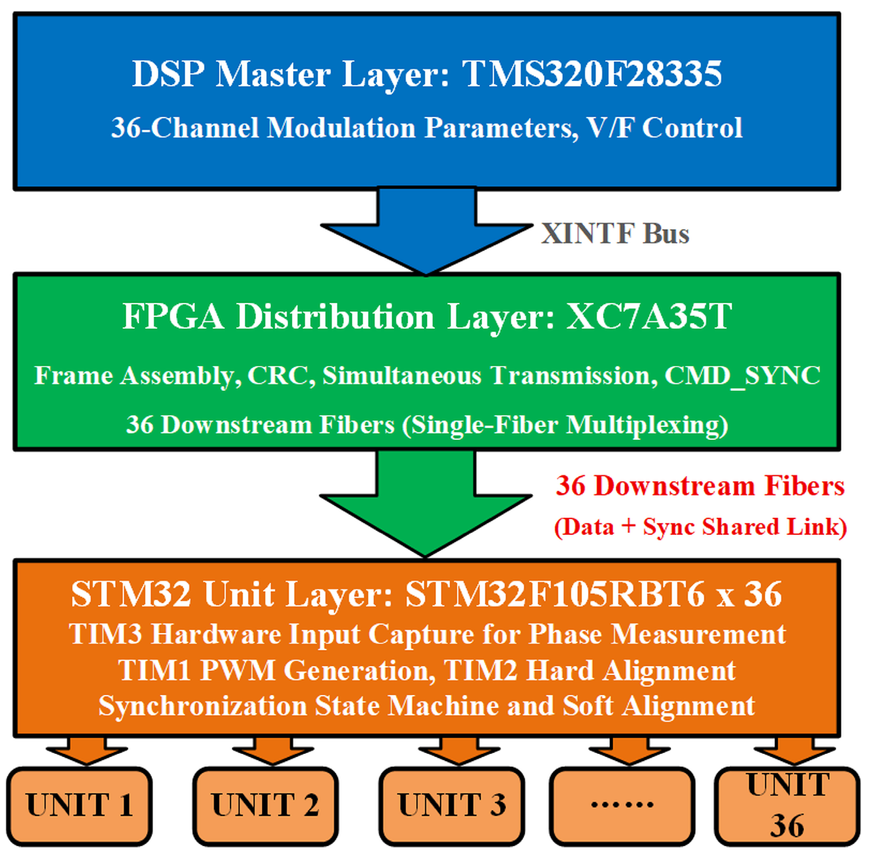
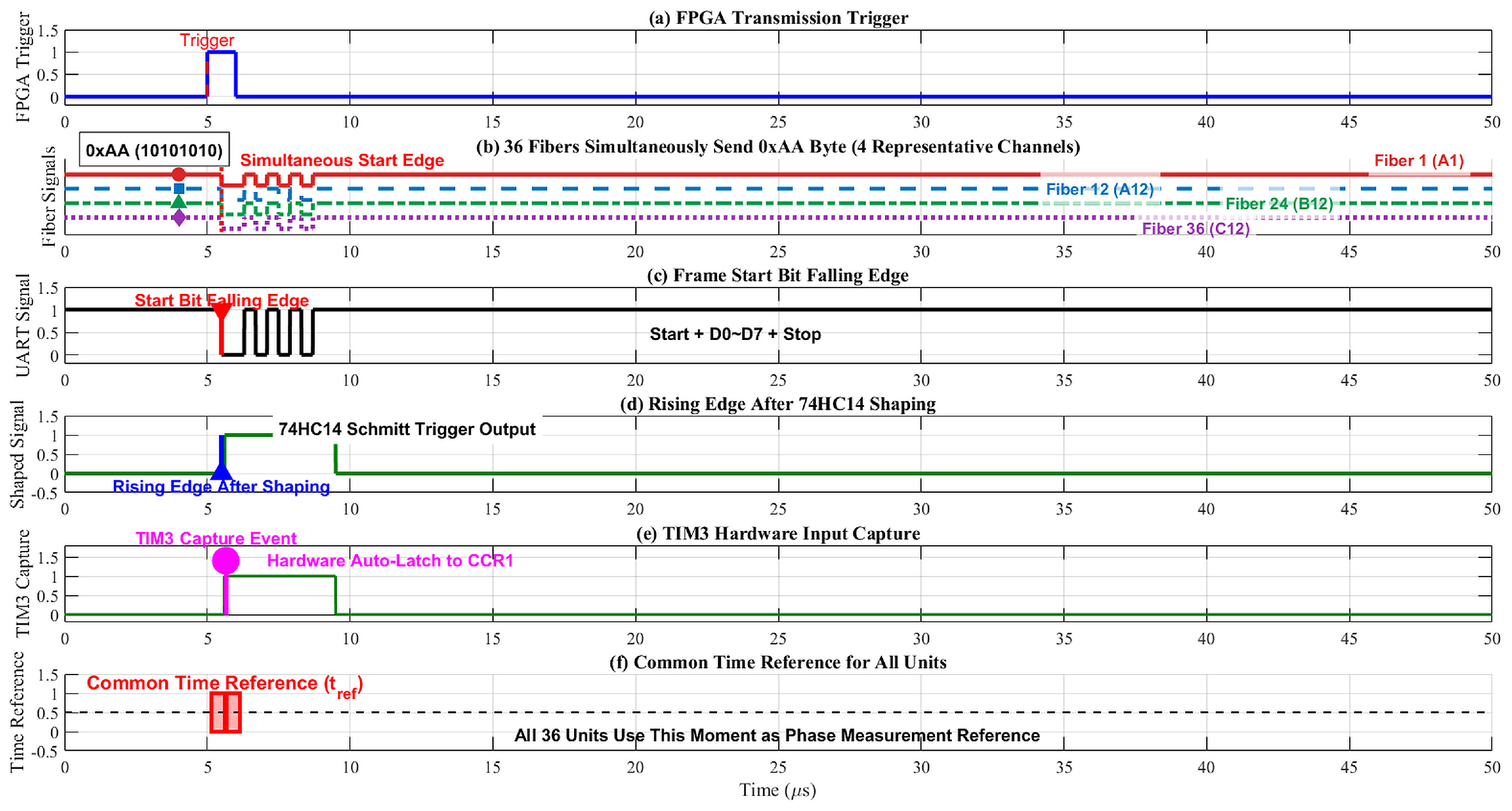
At the architectural level, a multiplexing architecture is proposed in which the start edge of the downlink data frame serves as the common time reference and synchronization frames are identified by a synchronization flag bit within the command byte. No dedicated synchronization fiber is required for the 36-cell system, and the numbers of optical fibers and transceiver modules are reduced by 50% relative to the independent synchronization link scheme. Neither a bidirectional link nor cell addressing is required, and a unified firmware image, arbitrary interchangeability of cell positions, and dynamic configuration of 5 to 12 layers are supported.
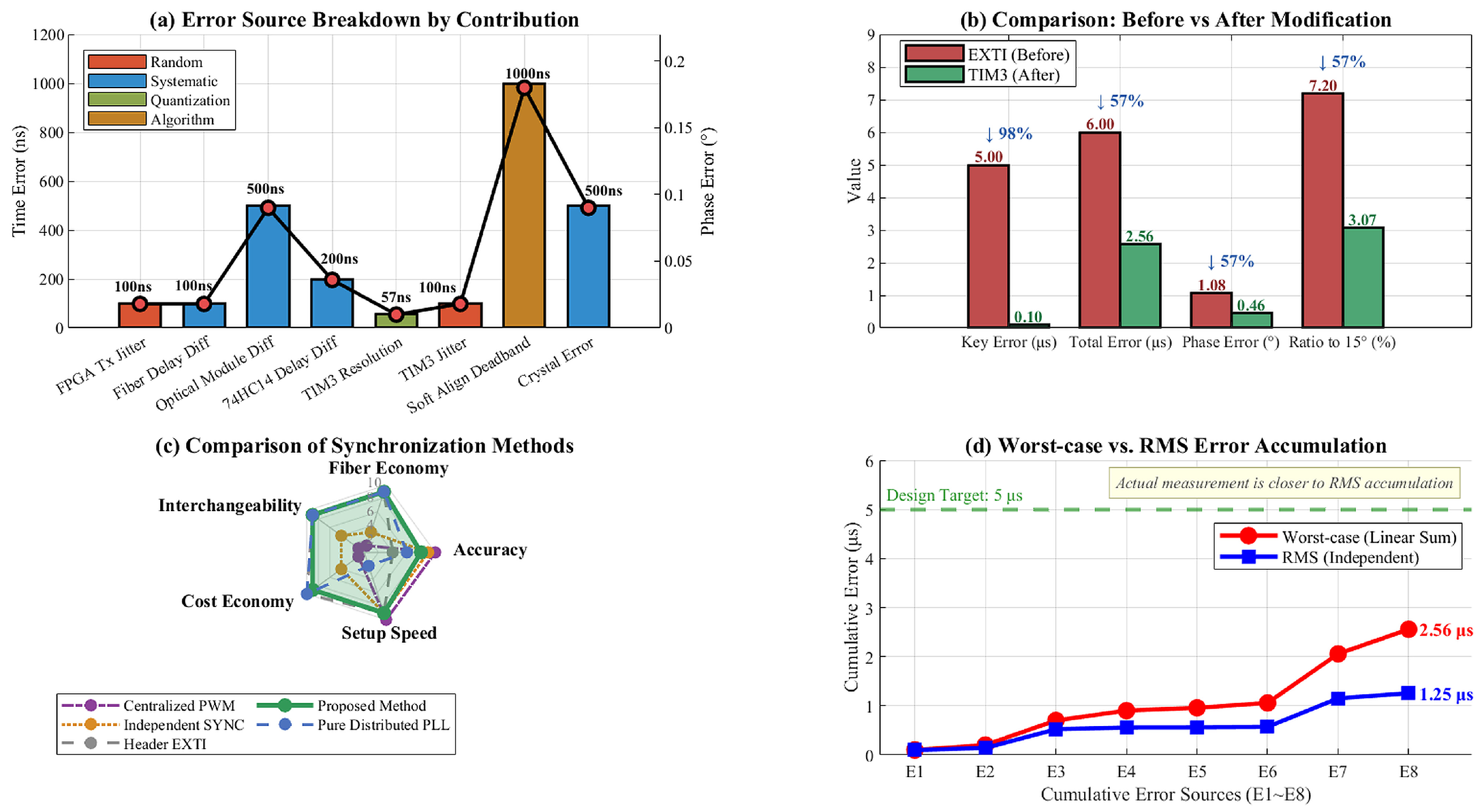
At the implementation level, hardware timer input capture replaces the external interrupt for acquiring the instant of the reference edge. The reference edge is latched automatically by the capture channel at the hardware level, so that interrupt-response latency no longer enters the phase-measurement path. This idea shares its origin with hardware timestamping in PTP; the contribution here lies in adapting it to a unidirectional broadcast link without protocol-stack support, using only three pin-to-pin connections and no printed-circuit-board redesign. The worst-case analytical budget predicts a reduction in the synchronization-error bound from above 6 μs for the EXTI scheme to below 2.56 μs for the proposed scheme; the EXTI value is not a same-platform experimental result.
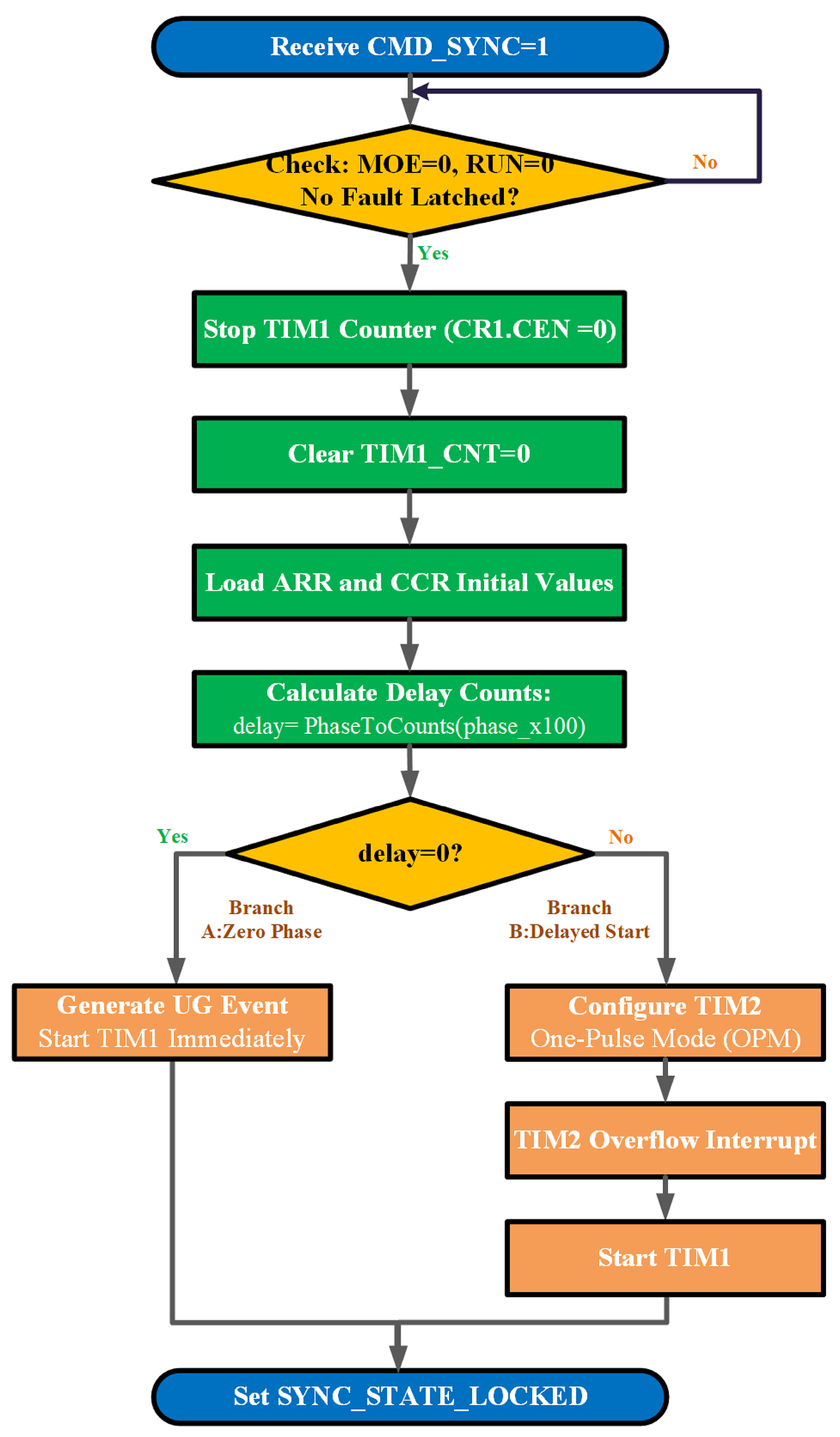
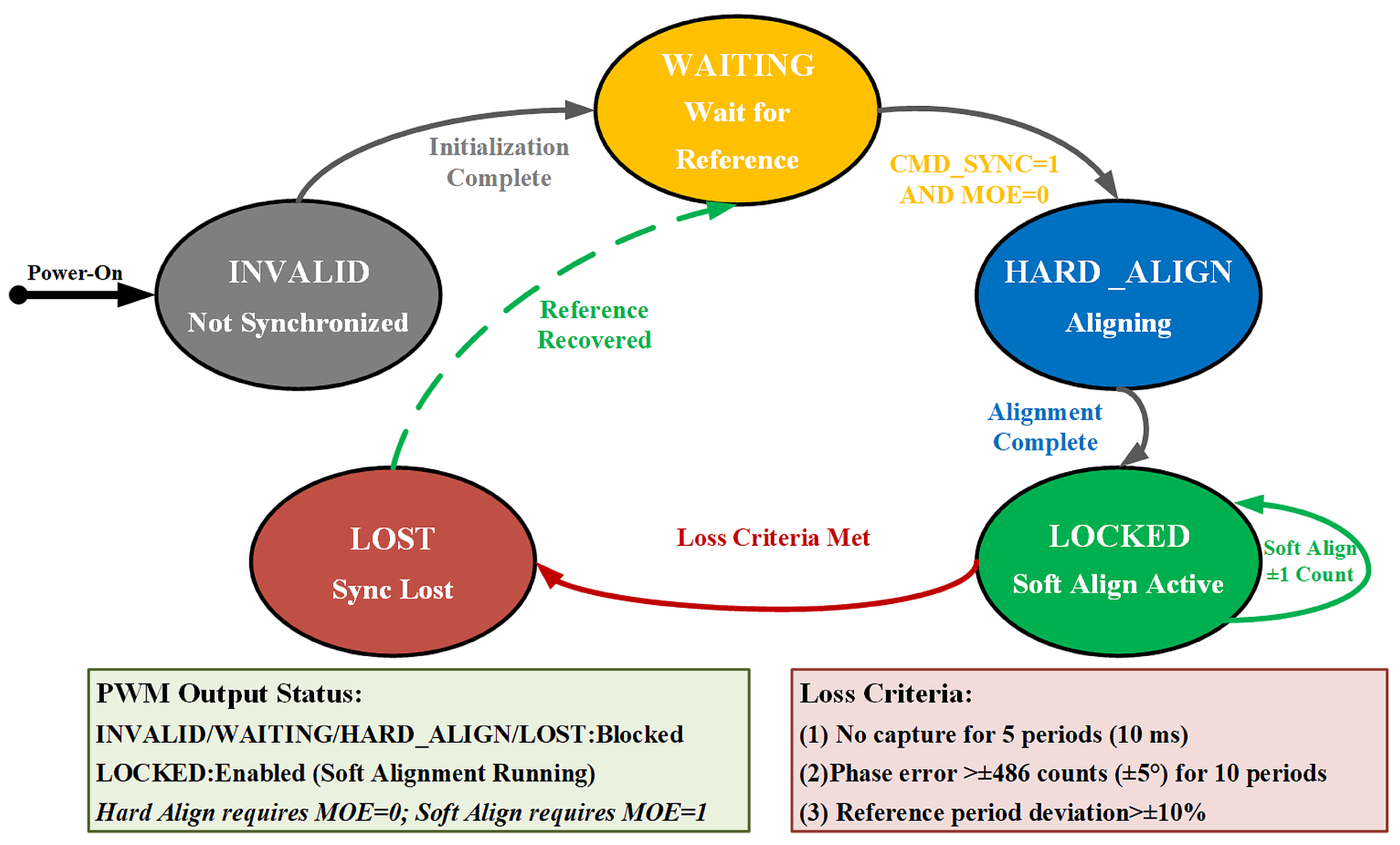
At the mechanism level, a dual-stage mechanism combining standstill hard alignment with on-line soft alignment is proposed. Hard alignment employs the one-pulse output mode of a timer to reconstruct a unified counter origin in a single operation during standstill, so that synchronization is established within one communication cycle; soft alignment suppresses the long-term drift caused by crystal oscillator frequency deviation through a rate-limited correction of no more than one timer count per carrier period during operation. In contrast to fully distributed phase locking, synchronization is established by hard alignment rather than through loop convergence, and soft alignment is responsible only for drift suppression; rapid convergence capability is therefore unnecessary, and establishment speed and output continuity are reconciled.
The remainder of this paper is organized as follows.
Section 2 analyzes the impact of synchronization error on the harmonic cancelation of CPS-SPWM and establishes the accuracy specification.
Section 3 describes the overall architecture and hardware implementation of the multiplexed synchronization scheme.
Section 4 presents the dual-stage hard and soft-alignment mechanism together with the synchronization state machine.
Section 5 gives the error budget and a comparison of the performance before and after modification.
Section 6 verifies the effectiveness of the scheme experimentally on a 13.8 kV, 36-cell prototype.
Section 7 concludes the paper and discusses open issues.
6. Experimental Validation
6.1. Experimental Platform
The experimental hardware is a 13.8 kV, 3 MW, 36-cell cascaded H-bridge soft-starter prototype with 12 cells per phase. The rating describes the prototype design; it does not mean that every test reported below was performed at 13.8 kV and 3 MW. The complete 36-cell controller and optical-link hardware was used for the timing, synchronization-loss, recovery, and long-duration tests at fc = 500 Hz. The single-phase cascaded-output waveform and FFT measurements were performed at 380 V. No full-power 13.8 kV/3 MW loaded waveform or EMC test is included in this study.
The test matrix comprises inter-cell phase-offset measurements, a 12-cell 380 V cascaded-output waveform and spectrum, a manual A6 fiber-interruption/recovery test, and an eight-hour coarse-sampled drift record. No controlled EXTI/TIM3 A/B test, oscillator-mismatch sweep, corrupted-frame injection campaign, active-layer-count sweep, cycle-resolved jitter acquisition, or full-voltage EMC test is included. The analytical and state-machine evaluations added in this revision are labeled separately from measured evidence.
The validation evidence is therefore classified by bandwidth and provenance.
Table 15 is a spatial accuracy test across cells,
Figure 8 is a low-bandwidth drift record, and
Figure 9 is a single physical link-interruption/recovery test. None of these records contains continuous per-carrier-cycle timestamps. Because such information cannot be reconstructed from the archived figures without inventing data, cycle-resolved short-term jitter is reported as unavailable rather than estimated from the 600 s drift samples.
6.2. Static Inter-Cell Carrier-Phase Accuracy Measurement
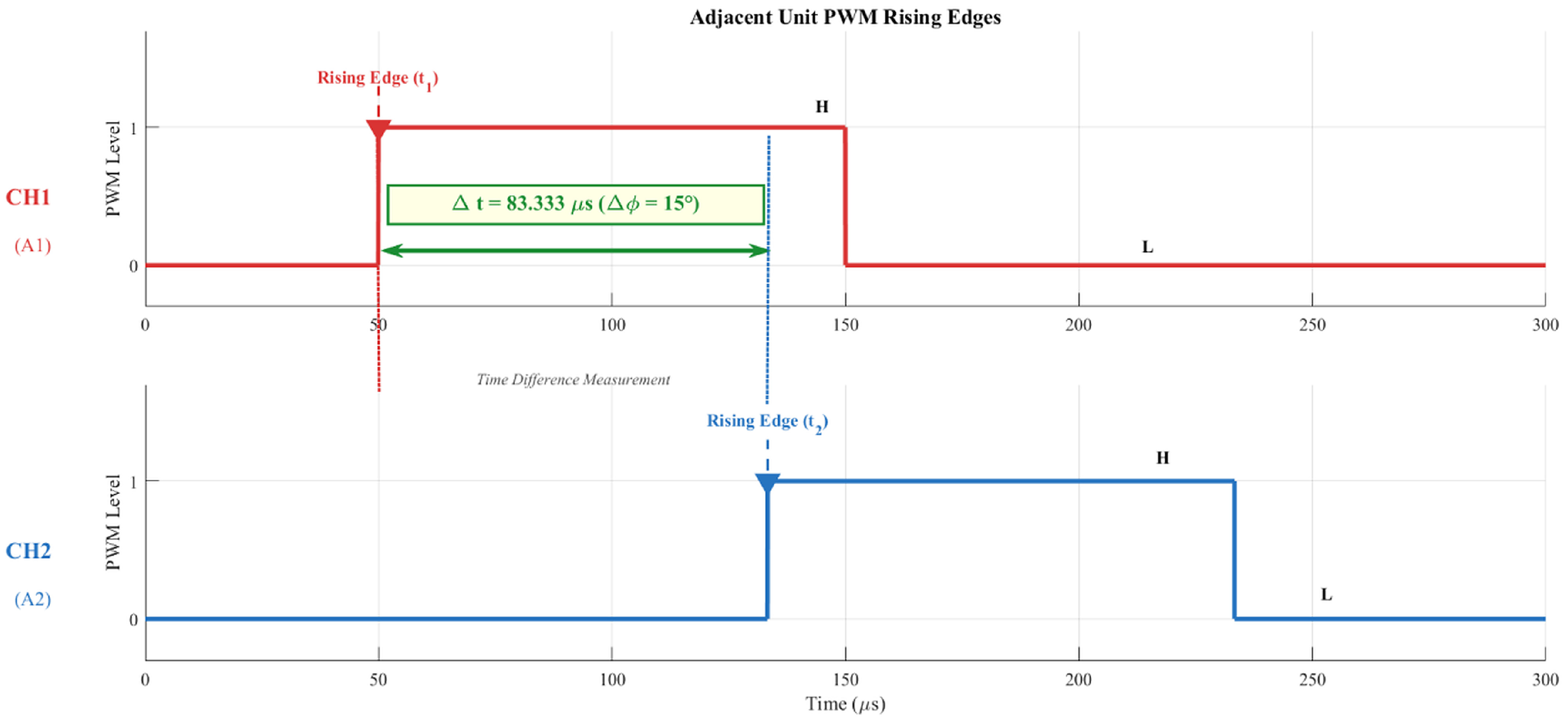
A dual-channel oscilloscope was used to observe simultaneously the PWM rising edges at PA8 (TIM1_CH1) of adjacent Phase-A cells A1 and A2. The theoretical interval is 83.333 μs, corresponding to 15° at fc = 500 Hz.
Figure 8 shows the measured waveforms.
Figure 8.
Adjacent unit PWM waveforms (A1 and A2); the PWM ordinate is a dimensionless logic level (0/1), and the abscissa is time in microseconds (μs).
Figure 8.
Adjacent unit PWM waveforms (A1 and A2); the PWM ordinate is a dimensionless logic level (0/1), and the abscissa is time in microseconds (μs).
Using A1 as the reference, the time offsets of A2 through A12 relative to A1 were measured in sequence; the measured data are shown in
Table 16. The phase angles were calculated from the time offsets as shown in Equation (30).
where
φmeasured is the measured phase angle in degrees (°), Δ
tmeasured is the measured time offset in microseconds (μs), and
Tc is the 2000 μs carrier period defined previously.
Table 16 reports the measured phase data for Phase-A cells relative to A1.
The maximum absolute phase-offset deviation is 0.36° at A4, A7, and A10. Using the 11 deviations listed in
Table 16, the root-mean-square deviation is calculated by Equation (31).
where
σφ is the RMS phase deviation,
εi is the
ith measured deviation, and
M = 11 is the number of deviations. Direct substitution of the
Table 16 data gives
σφ = 0.223°, reported as 0.22° after rounding. The maximum deviation of 0.36° is 2.4% of the 15° designed phase shift, and both statistics satisfy the criterion Δ
tsync < 5 μs (Δ
φerr < 0.9°).
These 11 values quantify cell-to-cell static phase-placement accuracy at the measured operating point. They do not constitute 11 temporal samples of one cell pair and therefore are not used to infer short-term jitter, peak-to-peak timing noise, or a jitter probability distribution.
6.3. Low-Voltage Cascaded-Output Waveform
To evaluate cascaded-output quality, the single-phase 12-cell output was tested at 380 V on the grid side, with modulation index
M = 0.8 and carrier frequency
fc = 500 Hz. This is a low-voltage functional test rather than a rated 13.8 kV/3 MW test. The measured waveform in
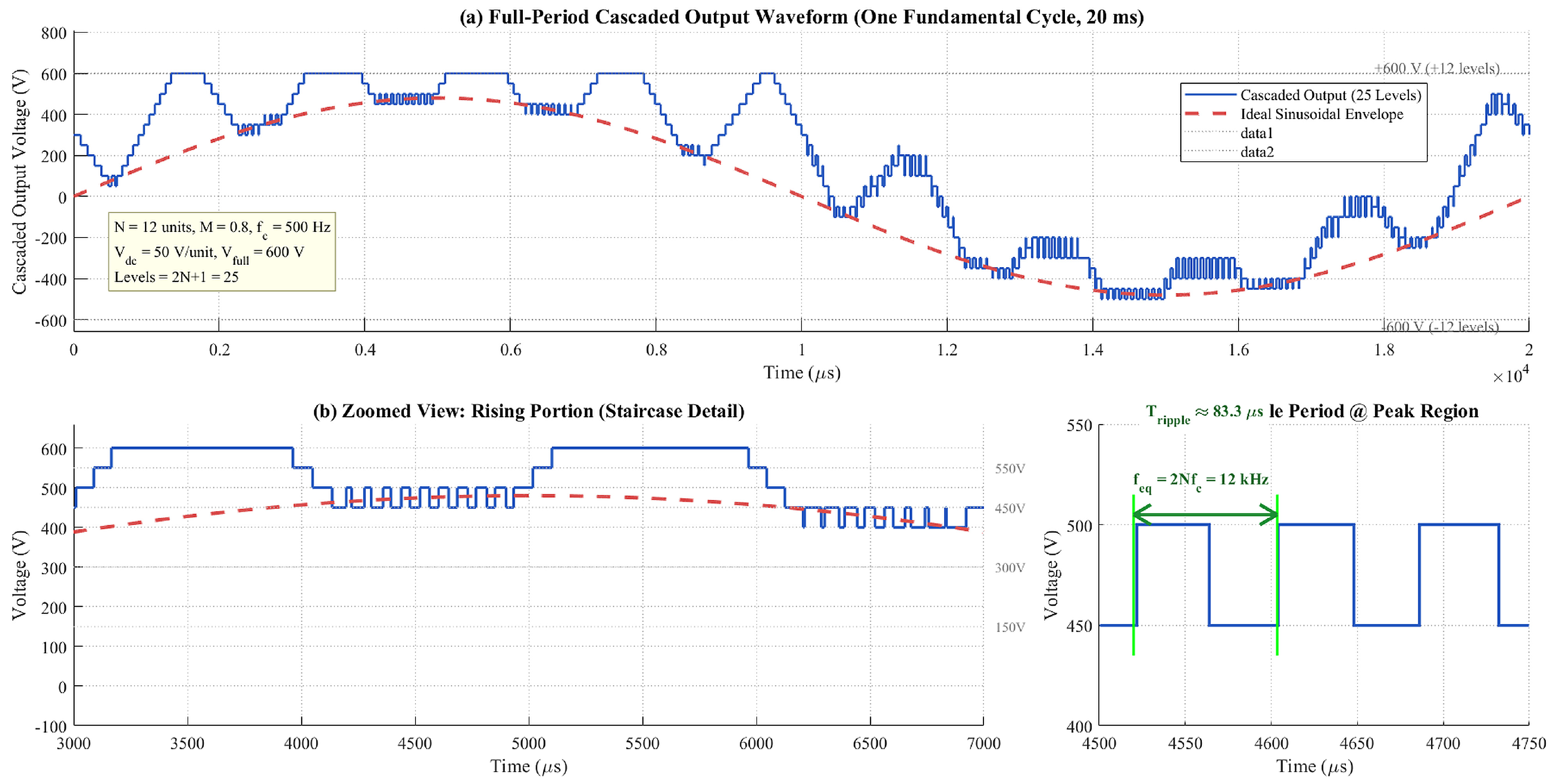
Figure 9 is a 25-level staircase with a sinusoidal envelope and a dominant ripple near 12 kHz.
Figure 9.
Measured single-phase 12-unit cascaded-output waveform.
Figure 9.
Measured single-phase 12-unit cascaded-output waveform.
Figure 9 presents the measured results of a single-phase 12-cell cascaded output from three perspectives: the full-cycle waveform, a magnified view of a local step, and the ripple period in the peak region. The full-cycle waveform shows that the output is a 25-level step wave, consistent with the theoretical number of levels, 2
N + 1 = 25, and the sine envelope is smooth; in the magnified view, the widths of each level are generally uniform, with no obvious level missing, repetition, or transition phenomena observed; and the ripple period in the peak region is approximately 83.3 μs, corresponding to an equivalent switching frequency of 12 kHz, which aligns with the theoretical value
feq = 2
Nfc. The test results indicate that the phase relationships among the carrier waves of each unit meet expectations, and the harmonic cancellation and level superposition effects of CPS-SPWM satisfy the design requirements.
6.4. Spectrum Analysis
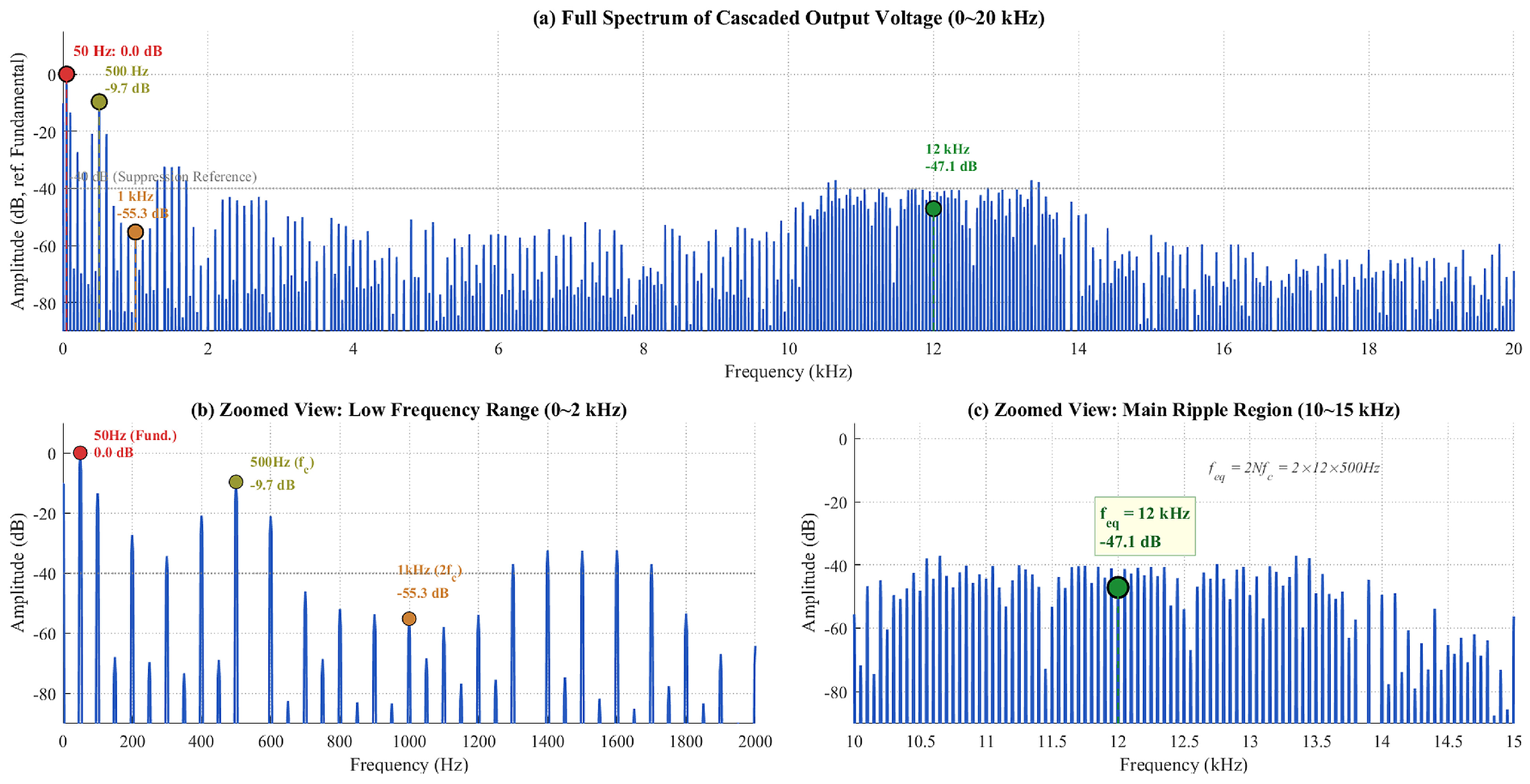
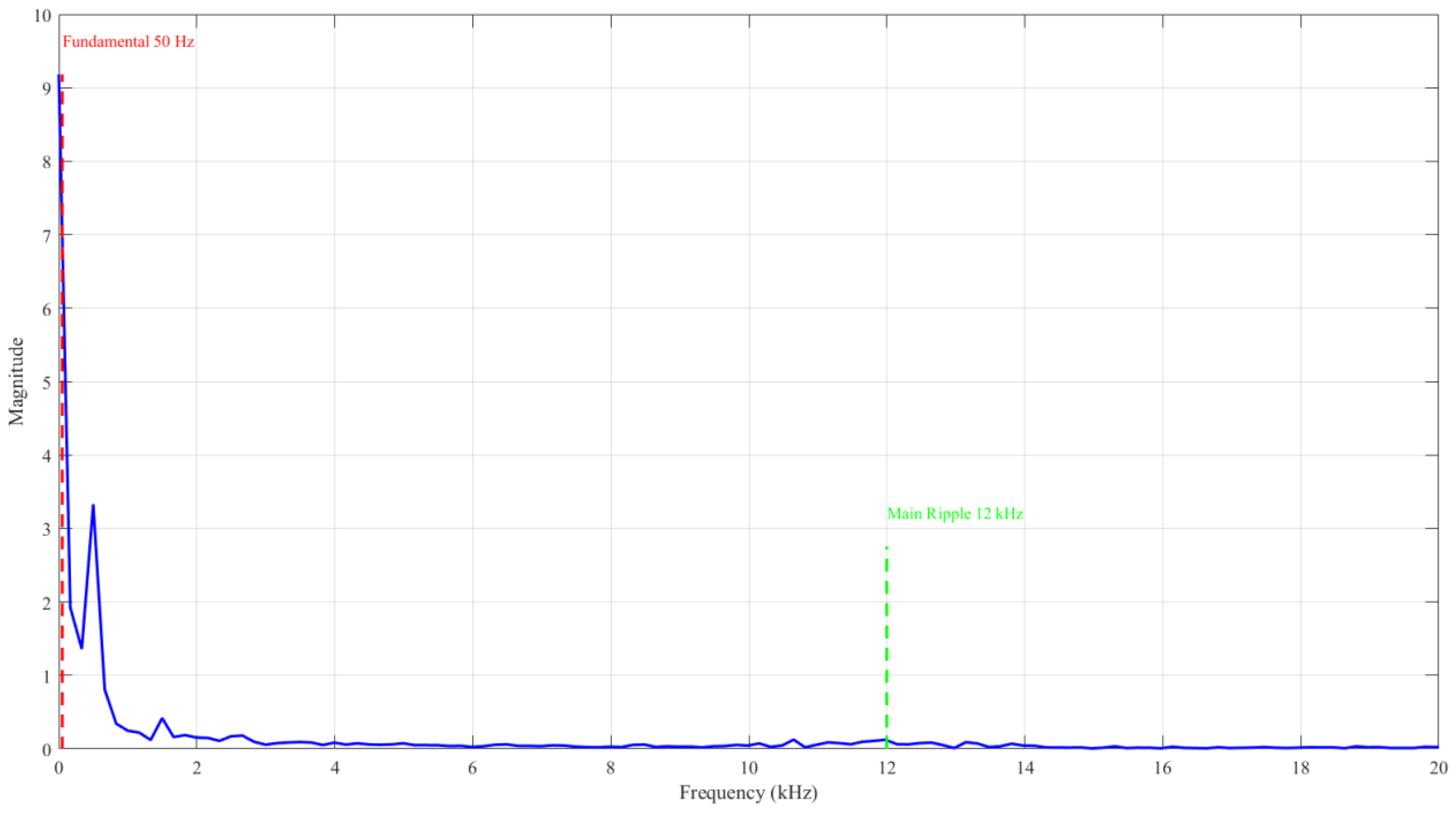
An FFT was applied to the 380 V single-phase cascaded-output voltage over 0–20 kHz.
Table 17 lists the measured components relative to the 50 Hz fundamental.
Figure 10 shows the FFT spectrum analysis results for the cascaded-output voltage.
Figure 10a displays the full spectrum from 0 to 20 kHz, with the majority of the energy concentrated at two frequency points: the 50 Hz fundamental and the 12 kHz main ripple; all other frequency components are below the −40 dB suppression reference line.
Figure 10b zooms in on the low-frequency band (2 kHz); the amplitudes of both the 500 Hz carrier sideband and the 1 kHz carrier second-harmonic sideband are below −42 dB, indicating that CPS-SPWM effectively cancels out the unit carrier-frequency components.
Figure 10c shows a magnified view of the main ripple region (10–15 kHz); the measured main ripple frequency matches
feq = 2
N ×
fc = 2(12) × (500 Hz) = 12 kHz. The spectral analysis results are consistent with the expected harmonic cancellation characteristics of CPS-SPWM, further validating the intended inter-cell carrier phase shifts under the 380 V test condition.
6.5. Loss-of-Synchronization and Recovery Test
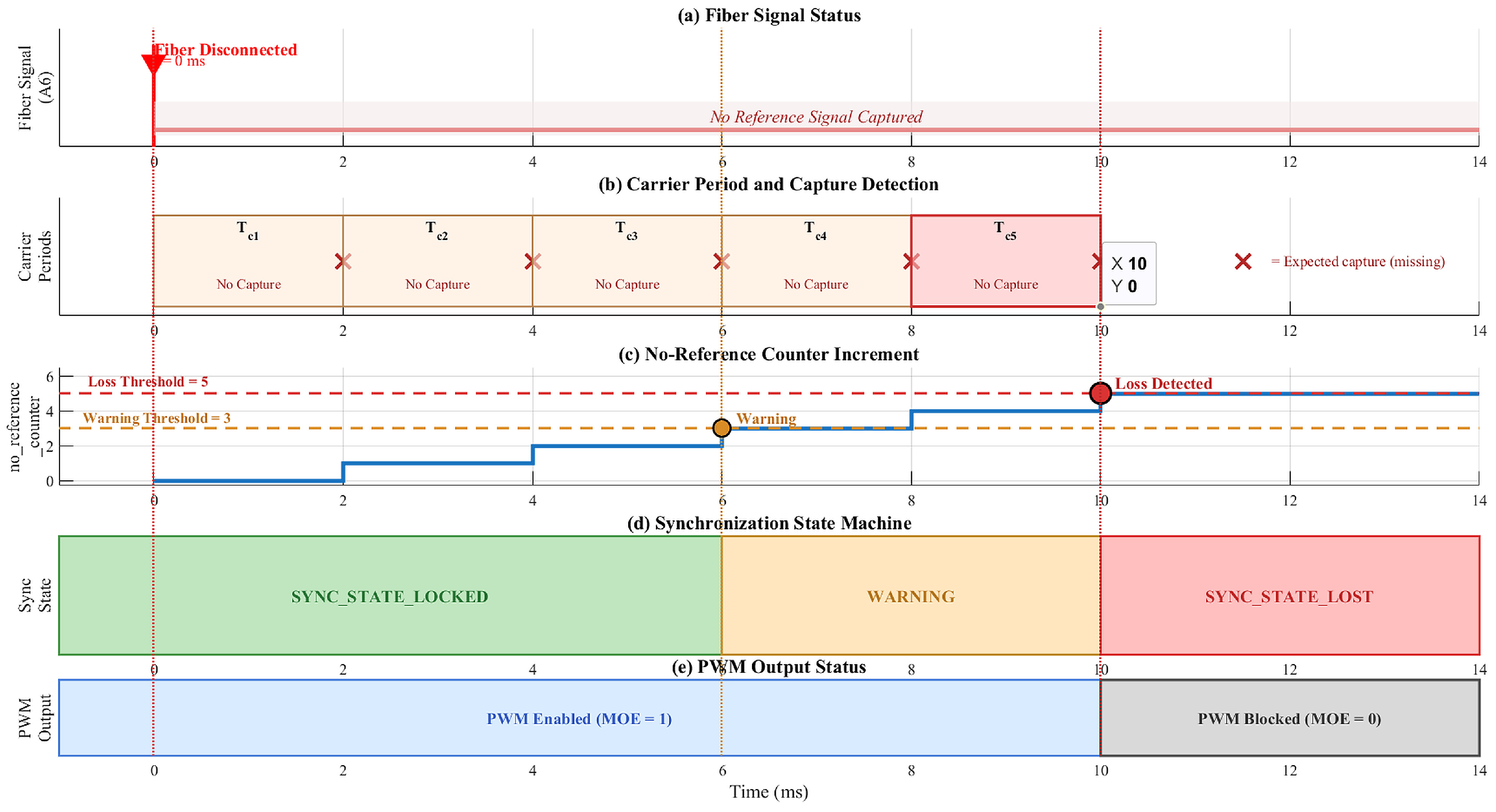
The only physical communication-disturbance experiment available for this revision was a manual interruption of the A6 downstream fiber, shown in
Figure 11. At
t = 0 ms the fiber was disconnected; after three missing valid references the alarm asserted at 6 ms, and after five missing references the controller entered SYNC_STATE_LOST and disabled PWM at 10 ms. Corrupted-frame, short-pulse, and intermittent-loss cases were evaluated against the implemented validation logic in
Table 10 but were not separately injected and measured.
Figure 11 confirms the measured missing-reference sequence for A6: the counter reaches the alarm threshold at 6 ms and the loss threshold at 10 ms, after which MOE is cleared and ST_SYNC_LOST is reported. The same deterministic counters apply to consecutive CRC-invalid or period-invalid frames because they do not produce a valid reference update; this is an implementation-level result, not an additional disturbance measurement.
After the A6 fiber was reconnected, a valid frame returned the unit to WAITING, CMD_SYNC = 1 initiated hard alignment, and LOCKED status was reported before the DSP restored system readiness. The measured end-to-end recovery time was below 2 s; this value includes command scheduling and status reporting and is not the hard-alignment pulse width. Under repeated failures the controller remains in LOST and does not re-enable PWM until a valid hard-alignment sequence is completed.
For brief communication disturbances, the implemented behavior is deterministic even though only the complete A6 interruption was physically injected in this revision. One or two consecutive invalid references (<6 ms) retain the previous alignment action without an alarm; three invalid references assert the synchronization alarm at 6 ms; five invalid references force the fail-silent LOST state and PWM blocking at 10 ms. Recovery from LOST is intentionally non-autonomous: a valid link first returns the unit to WAITING, after which a CMD_SYNC hard-alignment sequence is required before PWM can be re-enabled. This prevents burst errors or intermittent reconnection from causing an uncontrolled restart.
6.6. Coarse-Sampled Long-Term Drift Test and Resolution Limits
The complete 36-cell synchronization hardware operated for 8 h at
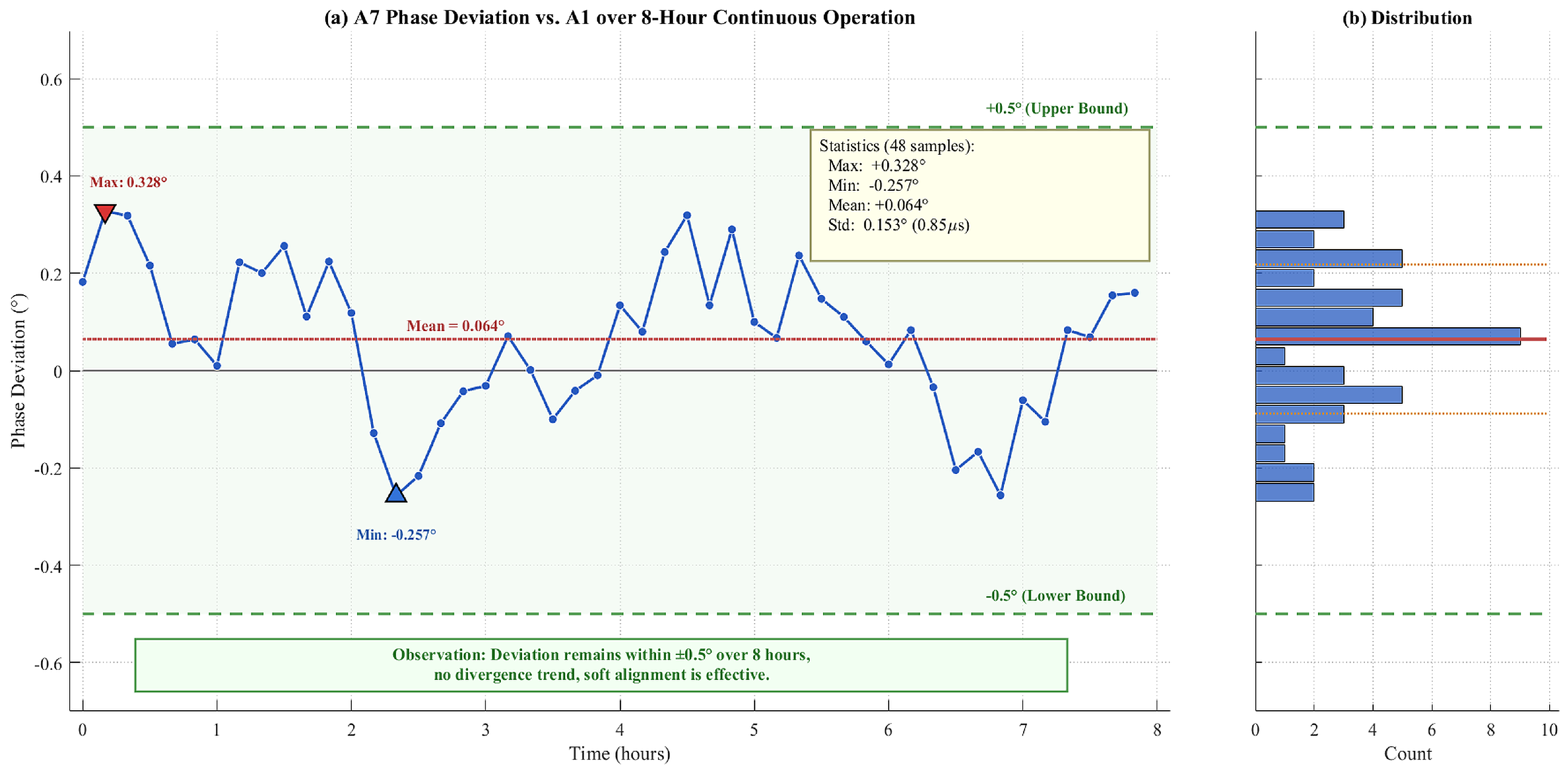
fc = 500 Hz under the low-voltage test supply. The A7-to-A1 phase offset was recorded once every 600 s, yielding 48 points. This corresponds to a sampling frequency of 1.667 mHz and a Nyquist frequency of only 0.833 mHz. The maximum, minimum, mean, and standard deviation shown by the retained 48-point record are +0.328°, −0.257°, +0.064°, and 0.153° (0.85 μs), respectively. These statistics and
Table 18 have been reconciled to the values embedded in
Figure 12; because the archived log values are available only through this coarse record, no finer effective reporting resolution is inferred.
Figure 12 shows no systematic trend in the 48 coarse samples, so it supports long-term drift stability under the laboratory condition. It cannot resolve cycle-to-cycle jitter, instantaneous peak-to-peak error, or a broadband statistical distribution. Those quantities require a continuous timestamped capture stream or oscilloscope histogram with stated analog bandwidth and trigger resolution, neither of which was preserved in the available data set. Accordingly, the terms ‘instantaneous jitter’ and ‘jitter distribution’ are not inferred from
Figure 12.
To obtain the higher-resolution short-term statistics requested for a future same-platform test, the capture register should be logged continuously at the 2 ms carrier rate (500 samples/s per monitored pair) for both EXTI and TIM3 paths under identical interrupt load, temperature, supply, and EMI conditions. The minimum report should include sample count and duration, timestamp resolution, RMS/standard deviation, maximum absolute error, peak-to-peak jitter, percentile limits, histogram or empirical CDF, and the measurement bandwidth. This protocol is stated here so that coarse drift stability and high-bandwidth jitter are not conflated.
Taken together, the measured tests verify inter-cell timing accuracy at selected points, fail-silent response to one fiber interruption, recovery logic, and 380 V waveform/spectral behavior. The eight-hour record verifies only low-frequency drift at the stated sampling resolution. Cycle-resolved jitter, multiple communication-fault modes, variable active-cell counts, a same-platform EXTI comparison, and full-voltage EMC immunity remain outside the measured evidence.