Article

A Hardware Input-Capture-Based Carrier Synchronization Method for Cascaded H-Bridge CPS-SPWM via Single-Fiber Multiplexing

by
Weibo Li
1,2,*,
Jiatao Tao
1,3,
Zixin He
1,
Cenhai Wang
1,
Chengying Yang
1,
Chiyu Peng
1 and
Tike Wu
1
1
School of New Energy and Electrical Engineering, Wuhan University of Technology, Wuhan 430070, China
2
School of Electrical Engineering, Northwest Minzu University, Lanzhou 730124, China
3
Hubei Zhongsheng Electric Co., Ltd., Xiangyang 441199, China
*
Author to whom correspondence should be addressed.
Energies 2026, 19(18), 4440; https://doi.org/10.3390/en19184440 (registering DOI)
Submission received: 10 August 2026 / Revised: 14 September 2026 / Accepted: 16 September 2026 / Published: 19 September 2026

Abstract

In cascaded H-bridge (CHB) high-voltage drives using unipolar frequency-doubling carrier phase-shifted sinusoidal pulse width modulation (CPS-SPWM), unequal carrier phase offsets weaken switching-harmonic cancelation. This paper proposes a carrier-synchronization method that improves timing accuracy without adding dedicated synchronization fibers. The start edge of the downlink data frame is multiplexed as the common timing reference, hardware timer input capture removes interrupt-response latency from edge acquisition, and a dual-stage strategy combines standstill hard alignment with rate-limited on-line soft alignment. A phasor model links synchronization error to residual carrier-group amplitude and establishes a conservative accuracy target below 5 μs. On a complete 36-cell prototype, the measured spatial root-mean-square phase-offset deviation across the 11 Phase-A cell pairs referenced to A1 is 0.22° (1.22 μs), and the maximum absolute inter-cell phase-offset deviation is 0.36° (2.00 μs). A 380 V cascaded-output test confirms the expected 12 kHz dominant ripple and strong suppression of the 500 Hz and 1 kHz sidebands. Compared with a dedicated synchronization-link architecture, the proposed scheme halves the fiber and transceiver counts, requires only three pin-to-pin connections per-cell controller, and preserves address-free unified firmware. The method therefore provides a practical accuracy-cost compromise for large CHB systems, while full-voltage electromagnetic-compatibility validation remains future work.

1. Introduction

The CHB converter achieves high-voltage output by connecting multiple low-voltage power cells in series. Owing to its modularity, ready scalability, and high output waveform quality, it has found application in medium-voltage variable-speed drives, static synchronous compensators (STATCOMs), and grid-connected photovoltaic inverters [1,2,3,4,5,6]. In high-voltage variable-frequency soft starters, up to 12 power cells are cascaded per phase, and by activating 5 to 12 cascaded layers according to the voltage rating, the application range from 6 kV to 13.8 kV can be covered.
Unipolar frequency-doubling CPS-SPWM is a control strategy widely adopted for CHB converters [7,8,9]. The strategy maintains uniformly spaced carrier phase offsets among the N cells within each phase. Since a single H-bridge cell already produces two voltage-level transitions per carrier period under unipolar frequency-doubling modulation, the optimal phase-shift increment is Δφc = 180°/N, which equals 15° for a 12-cell system. After superposition of the individual cell outputs, the dominant ripple frequency is raised from the carrier frequency fc of a single cell to an equivalent ripple frequency feq = 2Nfc. For N = 12 and fc = 500 Hz, feq = 12 kHz, that is, the switching frequency of each IGBT is only 500 Hz while the equivalent switching frequency of the cascaded output reaches 12 kHz, which reduces both switching losses and the output filter volume without compromising output waveform quality [10,11].
The above properties of CPS-SPWM presuppose that the carriers of all cells maintain strictly uniform phase offsets. When the phase offsets deviate from their ideal values, the carrier-frequency components and their sidebands, which are intended to cancel one another among the cell outputs, no longer cancel completely, and residual harmonics appear in the vicinity of the carrier frequency in the cascaded output, degrading the output waveform quality [9,12,13,14]. References [15,16] present theoretical, simulation, and experimental analyses of carrier phase-shift modulation for CHB and modular multilevel converter (MMC) systems, respectively. The results indicate that the carrier phase-shift angle directly affects the phasor superposition relationship of the switching harmonics in each power module; when the phase-shift angle deviates from a value conducive to harmonic cancelation, the residual carrier sideband harmonics increase, and the output voltage quality consequently deteriorates.
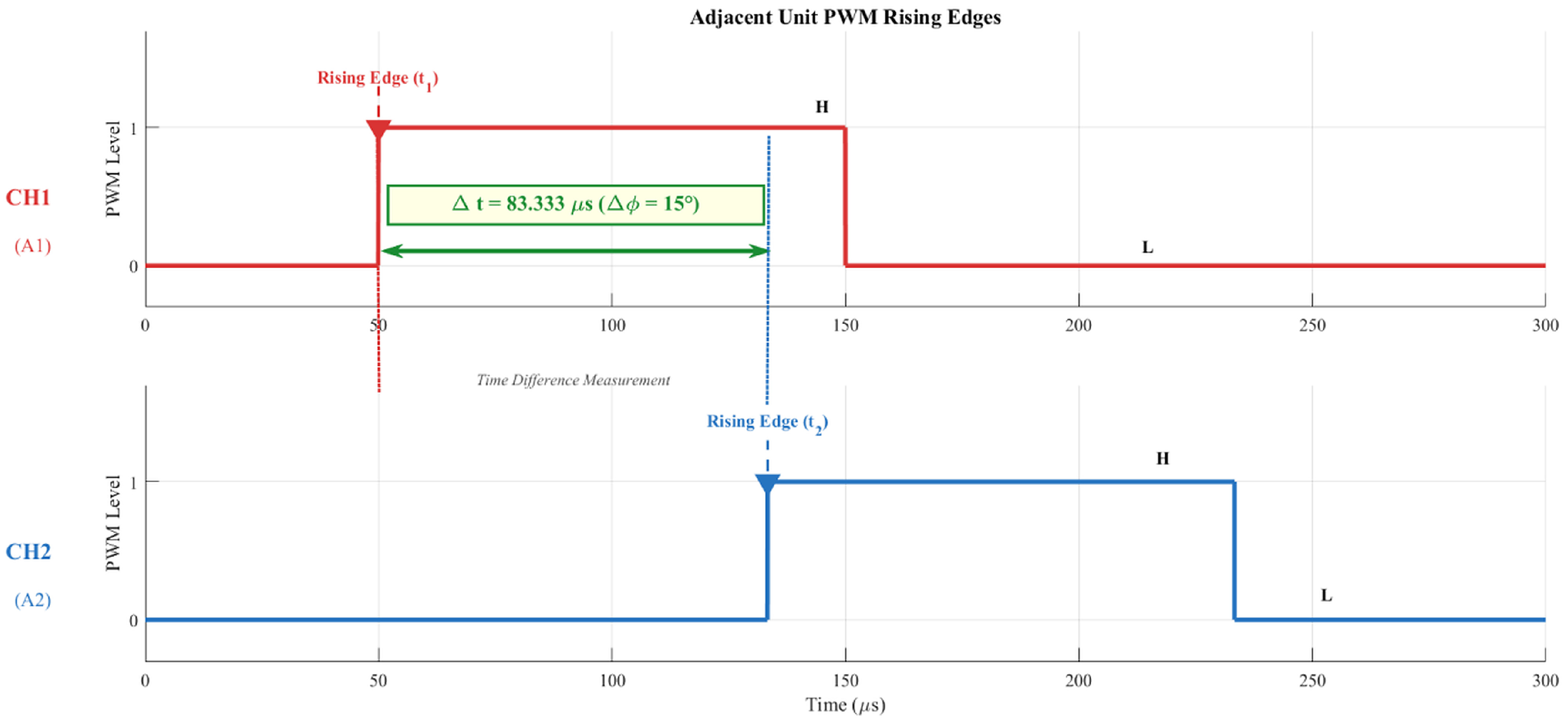
For a system with fc = 500 Hz (Tc = 2 ms) and Δφc = 15°, the theoretical phase-shift interval between adjacent cells is 83.333 μs. If the synchronization time error between cells is Δtsync, the corresponding equivalent carrier phase error is Δφerr = 360 fc Δtsync.
As shown by the analysis in Section 2.2, a carrier-phase error prevents exact phasor cancelation of the carrier groups. Table 1 reports a conservative upper bound for the normalized residual amplitude of the second canceled carrier group. At Δtsync = 5 μs, the equivalent phase error is 0.90° and the bound is −30.1 dB; at 10 μs, the phase error is 1.80° and the bound rises to −24.0 dB. The 5 μs criterion is therefore treated as a conservative design limit rather than an empirically optimized threshold.
For a 13.8 kV high-voltage soft starter comprising 36 power cells (12 per phase), the carrier synchronization scheme must be realized under the following engineering constraints. First, the cabinet wiring space and the number of wall bushings are limited, so the numbers of optical fibers and transceiver modules on the cell side should be kept as small as possible. Second, all power cells are programmed with an identical firmware image and are assigned no communication address, so as to permit arbitrary interchange of cell positions and the use of common spare parts. Third, dynamic activation of 5 to 12 cascaded layers according to the voltage rating must be supported. Fourth, the scheme should be realizable on the already finalized power cell hardware through minimal modification, without redesign of the printed circuit board, so that installed equipment can be upgraded.
Several approaches to inter-cell time synchronization have been reported in the distributed control of MMC systems. In centralized PWM generation, the master controller directly produces all gate drive signals within a single clock domain, so that no inter-cell synchronization error exists; however, 144 drive signals are required for 36 cells, and the insulation design on the high-voltage side together with signal integrity becomes difficult, which restricts this approach to small-scale systems of 3 to 5 cells [17]. The independent synchronization pulse line scheme provides each cell with a data fiber and a dedicated SYNC fiber, and each cell resets its local timer on the SYNC edge, achieving nanosecond-level accuracy at the cost of 72 fibers and 72 optical transceivers for 36 cells, which conflicts with the fiber count constraint of the present application [18]. In the field of industrial networks, the IEEE 1588 precision time protocol and the Ether CAT distributed clock achieve node synchronization by conveying timing information over the communication link; among the associated techniques, hardware time stamping latches the instant of the message edge directly at the physical layer, thereby avoiding the software jitter introduced by the protocol stack and interrupt handling, and can improve the synchronization accuracy to the sub-microsecond level [19,20,21,22]. These protocols, however, rely on bidirectional message exchange, node addressing, and a communication controller with timestamping support, whereas the link addressed in this paper is a unidirectional broadcast link built on low-cost plastic optical fiber transceivers with cells carrying no communication address, so that neither the protocol nor the hardware overhead can be accommodated. Against this background, engineering implementations commonly adopt frame-header external-interrupt synchronization, in which the start edge of the data frame serves as the common time reference, a general-purpose input/output (GPIO) external interrupt (EXTI) is triggered, and the timer count value is read in software to compute the phase error. This approach adds no optical fiber and is inexpensive, but the interrupt-response time is affected by the instruction being executed, interrupt priority preemption, and nesting, so that the jitter may reach the microsecond level [23]. Dedicated synchronization protocol symbols insert synchronization frames or characters into the data stream, and each cell performs phase alignment upon recognition; the identification is more explicit than a frame header, yet the method remains limited by software recognition latency and consumes communication bandwidth [24]. Fully distributed digital phase locking dispenses with a hard synchronization signal and converges slowly by means of a digital phase-locked loop acting on long-term error statistics; its disturbance immunity is strong, but the initial convergence time may reach tens of seconds, which fails to meet the rapid start-up requirement of soft starters [25]. A comparison of the conventional synchronization methods is presented in Table 2.
The progression of inter-cell synchronization has moved from centralized gating and dedicated point-to-point pulses to communication-link reuse, hardware timestamping, and distributed carrier-phase estimation. Recent electrical-variable-based methods [26,27] avoid a dedicated timing conductor, but they require current or voltage feedback, iterative phase estimation, and a convergence interval. Hardware-timestamped network methods provide higher accuracy, but normally require bidirectional exchange, node identities, timestamp-capable interfaces, and a clock-servo stack [19,20,21,22]. These approaches improve either accuracy or wiring efficiency, but none simultaneously provide a unidirectional broadcast link, address-free interchangeable CHB cells, one-cycle hard alignment, and no dedicated synchronization fiber. The contribution of this study is therefore the application-specific combination of frame-edge multiplexing, peripheral-level input capture, and hard/soft alignment. The evidence-controlled comparison in Table 1 reports synchronization accuracy, hardware and fiber requirements, establishment time, scalability, and per-cell computational burden without treating literature values as same-platform measurements.
Positioning relative to the state of the art is therefore important. The present contribution is not a new generic time-synchronization protocol, nor does it claim accuracy superior to dedicated SYNC fibers or hardware-timestamped bidirectional networks. Its novelty is the application-specific co-design of four functions that are usually treated separately: (i) reuse of the existing one-way downlink frame edge as the timing reference without node addressing or a second fiber; (ii) peripheral-level timer input capture so that CPU interrupt-response latency is removed from the timestamp path; (iii) one-cycle standstill hard alignment followed by rate-limited on-line correction; and (iv) preservation of identical, address-free cell firmware and cell interchangeability. This combination directly targets CHB installations in which wiring density, retrofit constraints, and deterministic microsecond-level synchronization are more important than sub-microsecond network time transfer.
Table 2 reveals a clear trade-off between synchronization accuracy and link cost in the existing methods: those satisfying the fiber count constraint are limited by software latency and offer indeterminate accuracy, whereas those attaining high accuracy either require a doubled fiber resource or presuppose bidirectional protocol support that the present link does not provide. The problem addressed in this paper is therefore how to raise the synchronization accuracy to a level meeting the harmonic cancelation requirement of CPS-SPWM under the conditions of a unidirectional low-cost link, cells without addresses, and minimal hardware modification.
To this end, this paper proposes a carrier synchronization method for CHB CPS-SPWM power cells based on multiplexing the communication data link with the synchronization reference. The work comprises four aspects.
At the analytical level, the switching-function coefficient of each canceled carrier group is factorized into a modulation-dependent term and an inter-cell phase-sum term. This yields an exact residual expression and a small-angle approximation whose error is quantified over carrier-phase errors from 0.18° to 15°. The same factorization supplies a generalized design procedure in which the allowable synchronization error depends on the number of cells N, carrier frequency fc, modulation index M through the selected harmonic coefficient, and the permitted residual-harmonic limit. The 5 μs value is recovered only as the design point for N = 12, fc = 500 Hz, M within the linear modulation range, and a −30.1 dB residual bound; it is not asserted as a universal threshold.
At the architectural level, a multiplexing architecture is proposed in which the start edge of the downlink data frame serves as the common time reference and synchronization frames are identified by a synchronization flag bit within the command byte. No dedicated synchronization fiber is required for the 36-cell system, and the numbers of optical fibers and transceiver modules are reduced by 50% relative to the independent synchronization link scheme. Neither a bidirectional link nor cell addressing is required, and a unified firmware image, arbitrary interchangeability of cell positions, and dynamic configuration of 5 to 12 layers are supported.
At the implementation level, hardware timer input capture replaces the external interrupt for acquiring the instant of the reference edge. The reference edge is latched automatically by the capture channel at the hardware level, so that interrupt-response latency no longer enters the phase-measurement path. This idea shares its origin with hardware timestamping in PTP; the contribution here lies in adapting it to a unidirectional broadcast link without protocol-stack support, using only three pin-to-pin connections and no printed-circuit-board redesign. The worst-case analytical budget predicts a reduction in the synchronization-error bound from above 6 μs for the EXTI scheme to below 2.56 μs for the proposed scheme; the EXTI value is not a same-platform experimental result.
At the mechanism level, a dual-stage mechanism combining standstill hard alignment with on-line soft alignment is proposed. Hard alignment employs the one-pulse output mode of a timer to reconstruct a unified counter origin in a single operation during standstill, so that synchronization is established within one communication cycle; soft alignment suppresses the long-term drift caused by crystal oscillator frequency deviation through a rate-limited correction of no more than one timer count per carrier period during operation. In contrast to fully distributed phase locking, synchronization is established by hard alignment rather than through loop convergence, and soft alignment is responsible only for drift suppression; rapid convergence capability is therefore unnecessary, and establishment speed and output continuity are reconciled.
The remainder of this paper is organized as follows. Section 2 analyzes the impact of synchronization error on the harmonic cancelation of CPS-SPWM and establishes the accuracy specification. Section 3 describes the overall architecture and hardware implementation of the multiplexed synchronization scheme. Section 4 presents the dual-stage hard and soft-alignment mechanism together with the synchronization state machine. Section 5 gives the error budget and a comparison of the performance before and after modification. Section 6 verifies the effectiveness of the scheme experimentally on a 13.8 kV, 36-cell prototype. Section 7 concludes the paper and discusses open issues.

2. Analysis of the Impact of Synchronization Errors on CPS-SPWM

2.1. Ideal Carrier Phase Shift and Equivalent Ripple Frequency

Under ideal CPS-SPWM conditions, the carrier phase angles of the N units per phase are expressed by Equation (1).
φ c , k = k Δ φ c k = 0 , 1 , , N 1
where φc,k represents the carrier phase angle of the kth unit, in degrees (°); Δφc represents the carrier phase shift, in degrees (°); k is the unit index; and N is the number of units per phase. For a 12-element system, the phase angles of each element are, in order, 0°, 15°, 30°, 45°, 60°, 75°, 90°, 105°, 120°, 135°, 150°, and 165°.
A single H-bridge uses unipolar modulation, with a three-level output (+Vdc, 0, −Vdc). The number of output levels for N units connected in a series is given by Equation (2).
L = 2 N + 1
where L denotes the number of voltage levels. For N = 12, the theoretical output is 25 voltage levels.
In an ideal CPS-SPWM system, the carrier frequencies of adjacent cells are offset by 1/N of a carrier period, resulting in the main ripple frequency of the cascaded output as shown in Equation (3).
f eq = 2 N f c
where feq is the equivalent ripple frequency, measured in hertz (Hz); fc is the carrier frequency, measured in hertz (Hz). When N = 12 and fc = 500 Hz, feq = 12 kHz. The switching frequency of a single unit is fc = 500 Hz, resulting in relatively low IGBT switching losses; the main ripple frequency of the cascaded output is feq = 12 kHz, allowing for the use of a compact output filter. Compared to a single-stage inverter, the filter volume can be reduced by (2N)2 = 576 times (theoretical value) while maintaining the same output waveform quality.
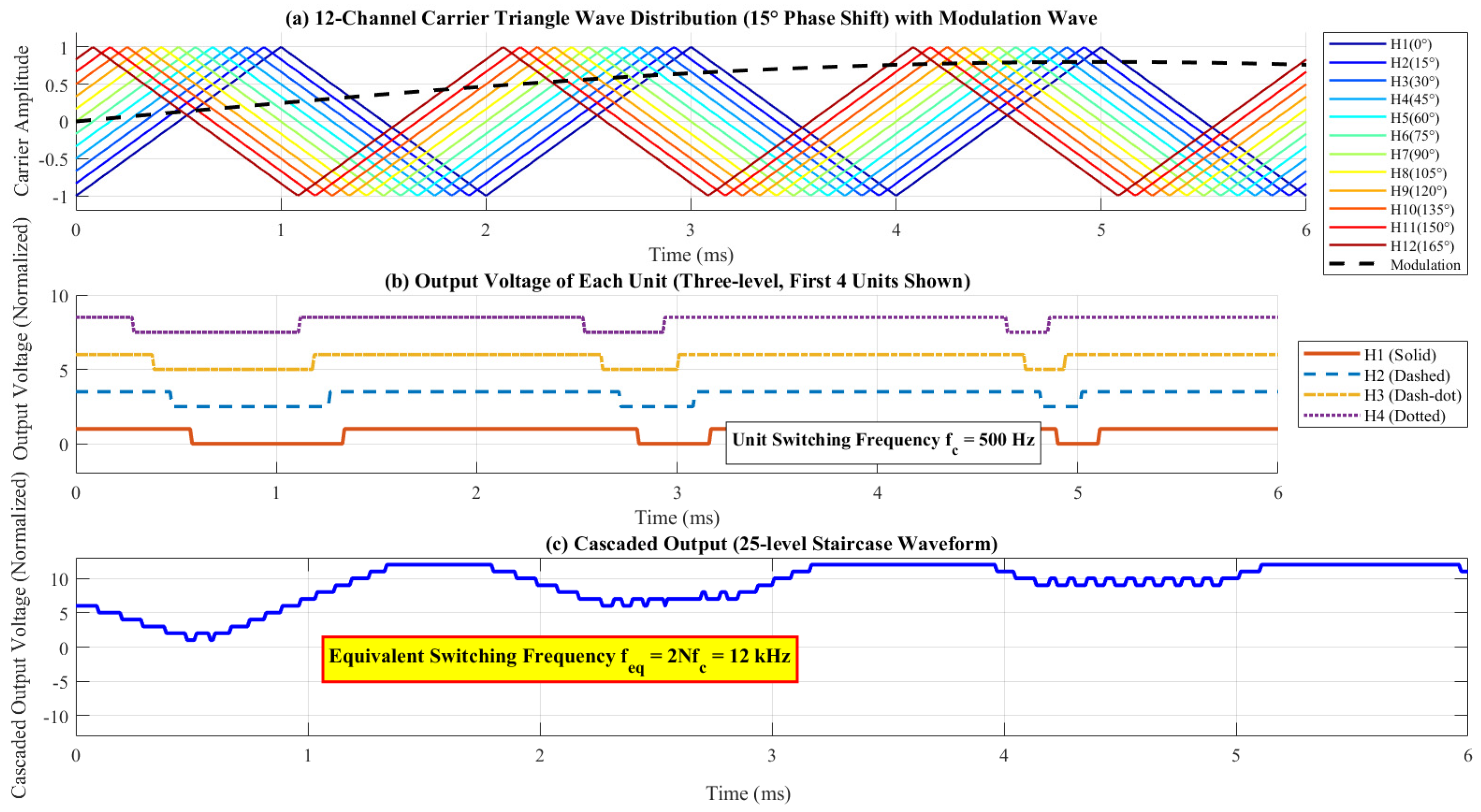
The ideal 12-cell CPS-SPWM carrier distribution and cascaded-output waveforms are shown in Figure 1.
Figure 1a illustrates the phase distribution of 12 triangular carrier waves; each offset by 15° relative to the next. The carrier waves from each cell are uniformly distributed within a single cycle, and when compared with a sinusoidal modulating wave, they generate PWM pulses. Figure 1b shows the three-level voltage waveforms (+Vdc, 0, −Vdc) output by each cell. Each cell operates independently at a switching frequency of 500 Hz, with different switching times achieved through carrier phase shifting. Figure 1c presents the 25-level staircase waveform output after the 12 cells are connected in series. Because the carrier phase shifting causes the switching actions of adjacent cells to be staggered, the equivalent switching frequency is increased to 12 kHz, and the output waveform approximates a sine wave.
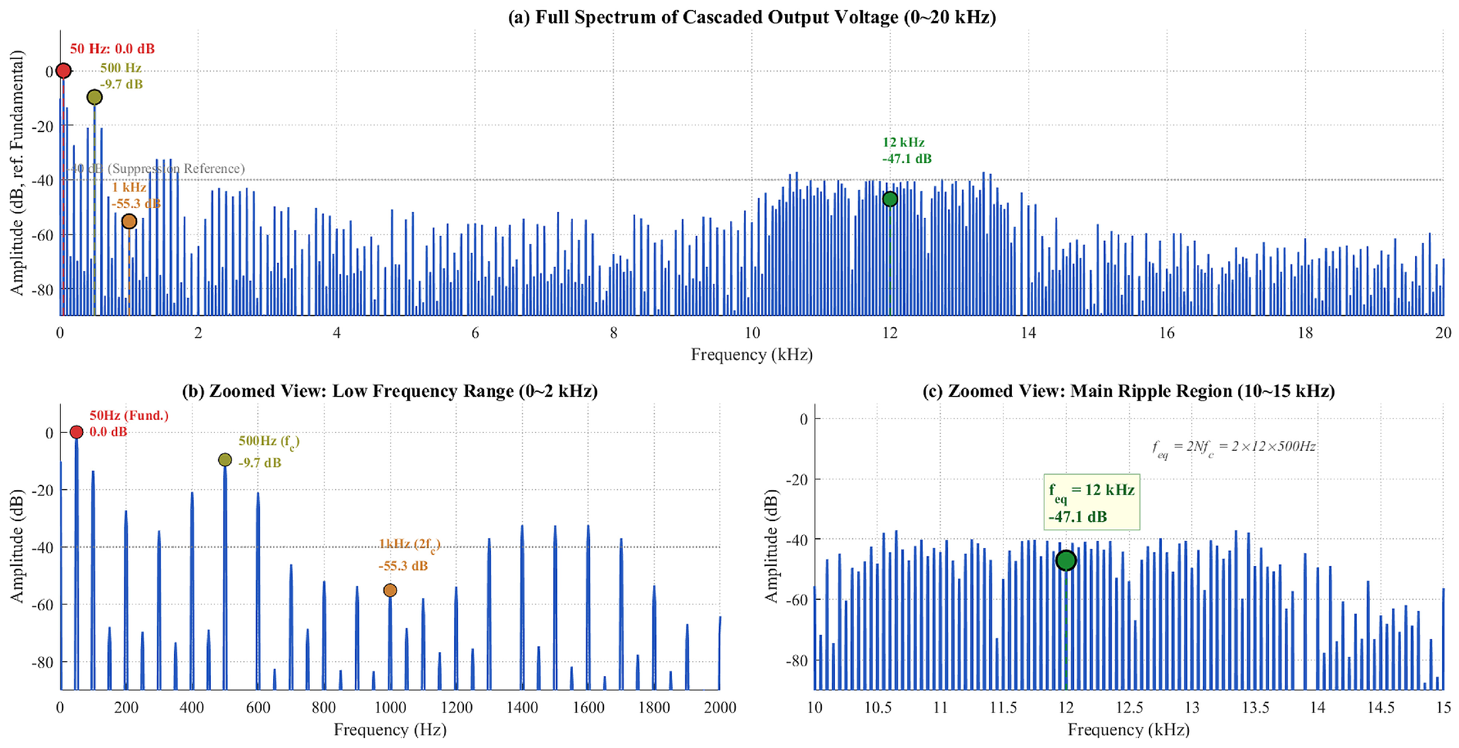
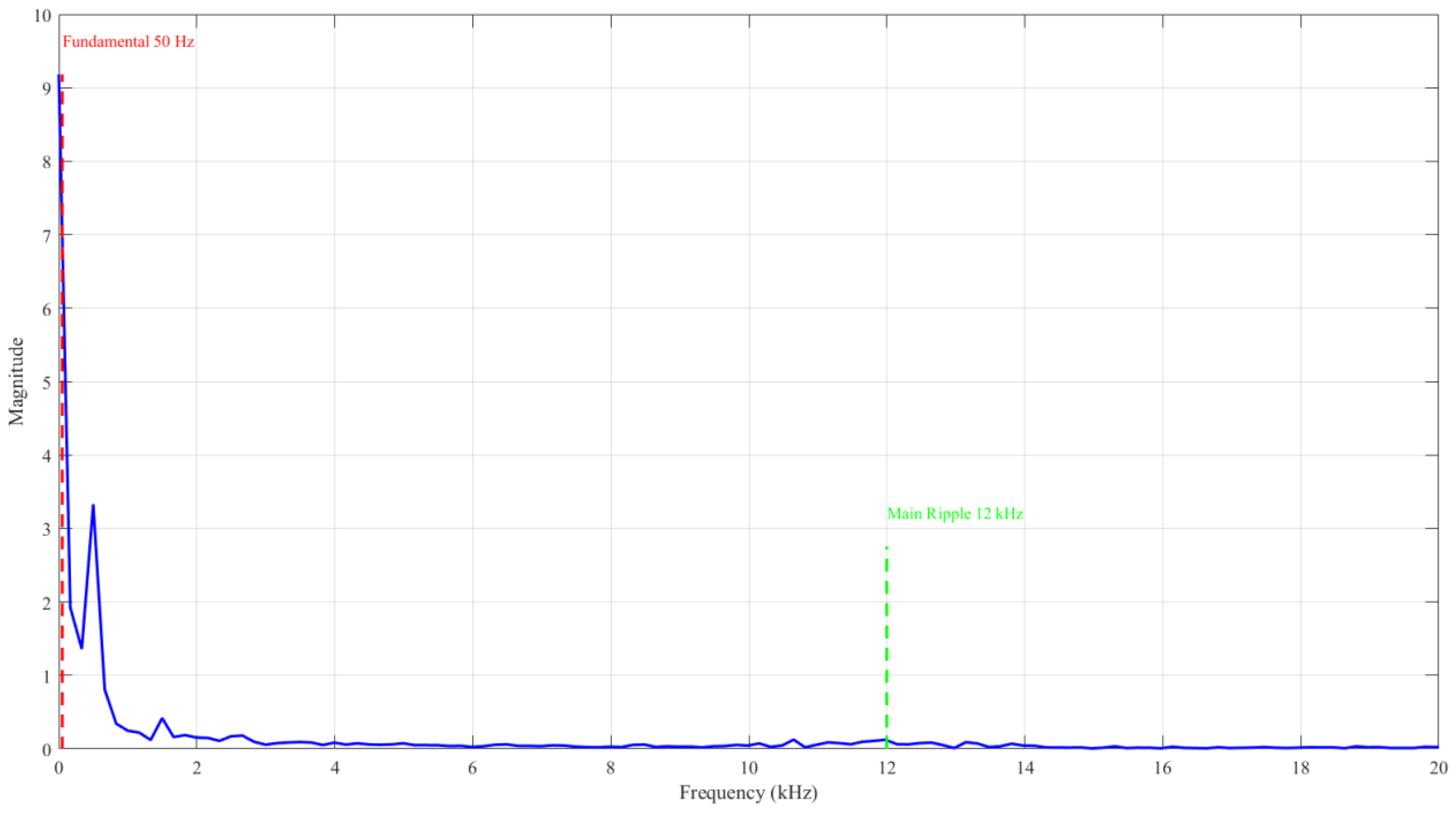
Figure 2 shows the spectral analysis of the cascaded-output voltage.
The spectrum in Figure 2 shows that the dominant ripple of the cascaded output is concentrated at 12 kHz, whereas the 500 Hz cell-carrier component and its low-order multiples are strongly attenuated by carrier phase shifting.

2.2. Quantitative Relationship Between Phase Error and Harmonic Cancelation Deterioration

Let the actual carrier phase angle of the kth cell be φc,k + εk, where εk is the phase error, measured in degrees (°). The phase error causes the switching times of adjacent cells to no longer be strictly equidistant; certain levels may persist for too long or too short a time, and some levels may be repeated or omitted. This results in a reduction in the equivalent switching frequency component and an increase in low-frequency harmonics [12,28].
A preliminary timing-scale screen is obtained by comparing the standard deviation of the time error, σε, with the carrier period Tc. The often-used 5% screen gives Equation (4); however, for this system it corresponds to 100 μs and is therefore much too loose relative to the 83.333 μs adjacent-cell spacing. It is retained only to show why a harmonic-based criterion is required and is not used as the final design limit.
σ ε T c 5 % σ ε 0.05   2 ms = 100   μ s
where σε is the standard deviation of timing error in microseconds (μs) and Tc is the carrier period in milliseconds (ms). Converting that screening value to carrier phase gives Equation (5).
σ φ = 360 f c σ ε = 18
where σφ is the standard deviation of carrier-phase error in degrees (°) and fc is the carrier frequency in hertz (Hz). The resulting 18° exceeds the designed 15° inter-cell shift, confirming that the 5% timing-period screen cannot protect harmonic cancelation in the present CHB system.
Given that in a 12-cell cascaded system, errors in any pair of adjacent cells will affect the output and that these errors may accumulate [9,16], it is necessary in engineering practice to limit the phase error between any pair of cells to within 1°, as shown in Equation (6).
| ε k | 1 Δ t sync 1 360 f c = 1 360 × 500 5.56   μ s
where εk is the phase error of the kth unit, in degrees (°); Δtsync is the synchronization time error, in microseconds (μs); and fc is the carrier frequency, in hertz (Hz).
An exact switching-function factorization gives a more direct relationship. For carrier group m and sideband index n, the k-th-cell coefficient can be written as Am,n(M) exp{jm(φc,k + εk)}, where Am,n(M) is the single-cell Fourier coefficient determined by modulation index M and εk is expressed in radians. After summing N cells, the exact normalized residual is Rm,exact = |Σ exp{jm(φc,k + εk)}|/N. The ideal sum is zero for a canceled group. If |εk| ≤ εmax, the triangle inequality gives the exact bounded form Rm,exact ≤ 2 sin (max/2). Expanding the exponential about εk = 0 gives the linearized bound Rm,linmax. Hence the linear statement used in the manuscript is a first-order approximation to an explicit sine relation, not an assumed empirical law.
The modulation-dependent coefficient Am,n(M) multiplies both the ideal single-cell group and the residual group, so it cancels from the normalized phase-loss factor Rm for every M in the linear modulation range 0 < M ≤ 1. The absolute harmonic voltage still depends on M through Am,n(M), and the allowable normalized residual must therefore be selected from the applicable harmonic mask at the intended M. Table 3 evaluates the exact and linear bounds for the second canceled group (m = 2) from εmax = 0.18° to 15°. At the design point εmax = 0.90° (5 μs at 500 Hz), the linearization error is 0.0041%; it remains 0.127% at 5° and reaches 1.15% at 15°. The exact sine relation is used for the generalized criterion below, while the linear form is used only to explain local sensitivity.
The harmonic derivation is used under the following explicit assumptions: all cells share the same fundamental modulation reference and carrier frequency; dc-link-voltage and modulation-index mismatch are neglected in the phase-loss factor; dead time, device switching transients, and unequal cell voltage amplitudes are treated as separate nonidealities; and the analyzed residual is the component created solely by carrier-phase perturbation. Under these assumptions, the exact sine bound is the governing relationship. The linear expression is used only as a local sensitivity approximation when m|ε|max << 1 rad. Table 3 quantifies the approximation error rather than assuming linearity: at the 5 μs design point (εmax = 0.90°, m = 2) the relative error is 0.0041%, while it rises to 1.1515% at εmax = 15°. Hence all design limits are evaluated with the exact sine relation, and the linear form is retained only for interpretation.
Table 3 summarizes the exact-versus-linear validation range for the second canceled carrier group.

2.3. Synchronization-Accuracy Criterion

The 5 μs value in Equation (7) is the result of the following generalized design procedure evaluated for the prototype parameters; it is not prescribed independently of N, fc, or M.
Δ t sync < 5   μ s
The corresponding phase error limit is given by Equation (8).
Δ ϕ err < 0.9
For general design, let ρm(M,N) denote the largest acceptable normalized residual for the selected canceled carrier group m after the absolute harmonic limit has been mapped through the exact switching-function coefficient Am,n(M). The exact harmonic constraint is 2 sin (mπfcΔtsync) ≤ ρm, and therefore Δtharm = arcsin [ρm(M,N)/2]/(mπfc). A second geometric constraint limits the carrier error to a selected fraction α of the ideal inter-cell shift π/N, giving Δtgeom = α/(2Nfc). The allowable specification is Δtallow = min (Δtharm, Δtgeom, Δtimplementation). The cell count N determines the ideal phase spacing and the set of canceled groups; fc converts time error to phase error; and M enters through Am,n(M) and thus through ρm. For the present design, m = 2, α = 0.06, ρ2 = 0.031415 (−30.1 dB), N = 12, and fc = 500 Hz, so both Δtharm and Δtgeom equal 5.00 μs. With the same residual mask, N = 12 at fc = 1 kHz requires 2.50 μs, whereas N = 18 at fc = 500 Hz requires 3.33 μs because the geometric constraint becomes dominant. This procedure must be repeated when N, fc, M, or the harmonic mask changes.
For clarity, the 5 μs value is an engineering design specification, not a universal physical threshold or a value fitted to the experimental data. For the present prototype it is obtained by imposing two conservative requirements simultaneously: the second canceled carrier-group residual is limited to ρ2 = 0.031415 (−30.1 dB after normalization), and the carrier-phase error is limited to 6% of the ideal 15° inter-cell spacing (0.90°). Both constraints give 5.00 μs at N = 12 and fc = 500 Hz. The selected −30.1 dB/6% pair is therefore a declared design allocation for this prototype; a different harmonic mask, modulation range, cell count, or carrier frequency must be inserted into the generalized equations rather than reusing 5 μs unchanged.
Table 4 summarizes the conservative implementation allocations used to screen the proposed architecture against the 5 μs specification. The values are combined by worst-case linear addition to obtain the 2.56 μs (0.46°) bound. The 500 ns oscillator entry is a residual phase allocation rather than literal per-cycle drift and does not imply that the one-count soft-alignment loop covers the full ±30 ppm component tolerance.

3. Single-Fiber Multiplexed Synchronization Scheme

3.1. Overall Architecture

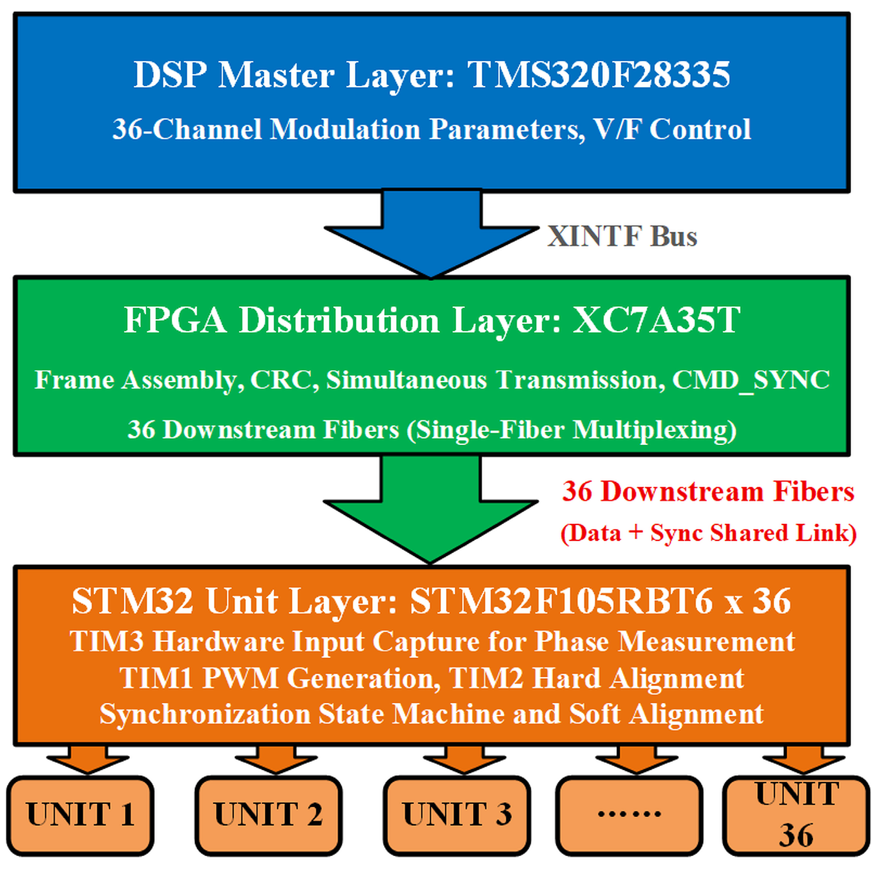
The proposed synchronization scheme has three layers, as shown in Figure 3. In the reference-generation layer, the FPGA launches the 36 downstream data frames from a common trigger; channel-to-channel launch uncertainty is handled explicitly in the error budget rather than claimed as an independently measured quantity. Bit 7 of the command byte (CMD_SYNC) identifies a hard-alignment frame. In the measurement layer, STM32 TIM3 latches the shaped frame-start edge in hardware, compares the capture with the TIM1 target count, validates frame and period consistency, and updates the synchronization state machine. In the execution layer, TIM1 and TIM2 reconstruct the counter origin during standstill and apply at most ±1 count per carrier period during operation. An invalid or missing reference is processed by the thresholds in Table 4; persistent failure disables PWM and recovery requires a new hard alignment.
Conventional frame-head synchronization schemes also utilize data frame edges, but they rely on GPIO external interrupts (EXTI) for capture, resulting in unpredictable software path delays [29]. The key improvement of this approach is to replace EXTI with TIM3 hardware input capture, thereby eliminating interrupt-response delays.

3.2. Reference Signal Definition and CMD_SYNC

The downlink data frame contains 10 bytes (Table 5): byte 0 is the fixed header 0xAA; byte 1 is the control word, with Bit 7 assigned to CMD_SYNC; bytes 2–3 contain the carrier phase angle scaled by 100 (0–16,500); bytes 4–5 contain the carrier frequency (100–2000 Hz); bytes 6–7 contain the duty ratio scaled by 1000 (0–1000); and bytes 8–9 contain the CRC-16/MODBUS checksum.
The bits of the command byte are defined as follows: Bit 0 is the run command (CMD_RUN), Bit 1 is the stop command (CMD_STOP), Bit 2 is the fault indication (CMD_FAULT), Bit 3 is the reset command (CMD_RESET), Bit 4 is the bypass close command (CMD_BYPASS_ON), Bit 5 is the bypass trip command (CMD_BYPASS_OFF), Bit 6 is the direction bit (CMD_DIRECTION), and Bit 7 is the synchronization alignment command (CMD_SYNC, newly defined). When CMD_SYNC = 1, this frame is used for synchronization alignment, allowing hard alignment to be performed while the unit is stopped; when CMD_SYNC = 0, it is a normal control frame.
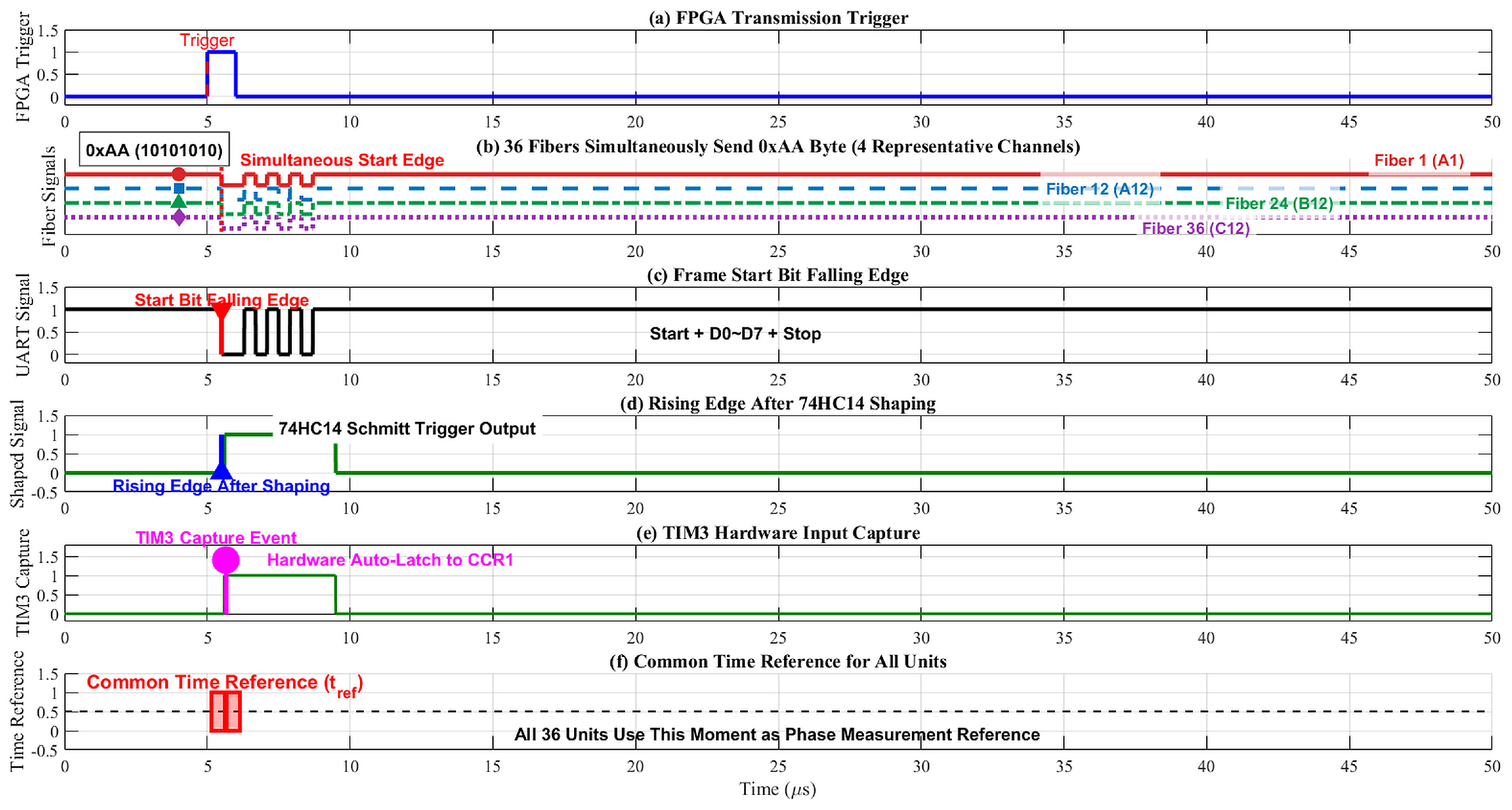
The falling edge of the UART start bit at the optical receiver, which becomes a rising edge after inversion and shaping by the 74HC14, serves as the common timing reference. The FPGA initiates the 36 downstream transmissions from a common trigger so that the frame-start edges reach the cells with only the channel-to-channel delay variations included in the error budget.
Figure 4a “FPGA Transmit Trigger”: The FPGA generates a unified transmit trigger signal at a fixed phase of the carrier cycle, which serves as the starting point for the simultaneous transmission of data frames over the 36 optical fibers.
Figure 4b “Simultaneous Transmission of 36 Fiber Channels”: The 36 downstream fiber channels transmit the first byte, 0xAA, at the same time, with the rising edges of each channel aligned and no phase shift applied to the transmission timing.
Figure 4c “Frame Start Bit Falling Edge”: That the start bit of a UART frame transitions from an idle high level to a low level; this falling edge serves as a timing reference that all units can recognize.
Figure 4d illustrates the “rising edge after shaping by the 74HC14”: The signal, after photoelectric conversion, is shaped and inverted by the 74HC14 Schmitt trigger, converting the falling edge of the start bit into a rising edge and improving the edge steepness.
Figure 4e “TIM3 Hardware Input Capture”: The shaped rising edge triggers a TIM3 input capture, and the hardware automatically latches the count value into the CCR1 register without going through the CPU interrupt path.
Figure 4f “Common Time Reference”: The TIM3 capture times form a common time reference for all 36 units. Each unit uses this as a baseline to compare with its local TIM1 target count and calculate the carrier phase error.

3.3. Hardware Input Capture as an Alternative to External Interrupts

PA12 is the TIM1_ETR pin. In the original design, the synchronization signal was connected to PA12 and configured as a GPIO external interrupt (EXTI). In that path, timestamp uncertainty includes the instruction in progress, interrupt priority and pre-emption, context entry, and the software counter read. Code-path and device-timing analysis gives an estimated 2–10 μs software-latency range, but this value was not measured in a same-platform A/B experiment and is treated only as an analytical baseline.
The hardware modification scheme involves shorting PA6 (TIM3_CH1), PA7 (TIM3_CH2), and PA12, and connecting the synchronization signal to all three pins simultaneously. TIM3 is configured in input-capture mode, and the hardware automatically latches the count value at the time the edge is detected into the CCR1 register. This modification does not require additional components or fiber optics, nor does it alter any external interfaces; it can be implemented via PCB jumpers or by modifying the board.
To ensure that the TIM3 capture value directly reflects the TIM1 phase, the two timers must maintain counting synchronization, as shown in Table 6. Configure TIM1 as the master timer, with the update event serving as the trigger output (TRGO), and configure TIM3 for slave mode reset. TIM1 operates in center-aligned mode with a pre-scaler (PSC) of 1, an auto-reload value (ARR) of 35,000, a count clock of 35 MHz, and a period of 2 ms (70,000 counts). TIM3 operates in up-count mode with PSC of 3, an auto-reload value (ARR) of 65,535, a count clock of 17.5 MHz, and free-running operation. As the slave timer, TIM3 is reset by the update event from TIM1 to maintain synchronization with TIM1. The count clock for TIM3 is 17.5 MHz, and its resolution is given by Equation (9).
Δ t res = 1 17.5 × 10 6 57.14   ns
where Δtres is the acquisition resolution, measured in nanoseconds (ns). One PWM cycle (2 ms) corresponds to a count as shown in Equation (10).
N period = 17.5 × 10 6 × 2 × 10 3 = 35000
where Nperiod is the count value for one PWM cycle. This value does not exceed the 16-bit range of TIM3 and meets the design requirements.
TIM3_CH1 is configured with TI1 (PA6) as the input, rising-edge capture, IC1F = 0011 (eight sampling cycles), and the capture interrupt enabled (CC1IE = 1). The digital filter rejects narrow pulses but introduces a bounded detection latency. Because all cells use the same setting, the common part of this latency does not affect relative phase; its channel-to-channel variation is covered by the shaping/capture allocations in Section 5.1 [30,31,32,33].

3.4. Phase Measurement and Error Calculation

Target count offset for each unit is converted from the ‘phase_x100’ field as shown in Equation (11).
N target = ϕ c , x 100 × f TIM 3 , CNT 36000 × f c
where Ntarget is the target count offset, φc,x100 is the phase angle multiplied by 100 (0–16,500), fTIM3,CNT is the TIM3 count frequency, and fc is the carrier frequency. For fTIM3, CNT = 17.5 MHz and fc = 500 Hz, the expression reduces to Equation (12).
N target = ϕ c , x 100 × 35 36
As shown in Table 7, the target offsets for each cell are as follows: Cell H1, φc,x100 = 0, phase angle 0°, Ntarget = 0, time offset 0 μs; Cell H2, φc,x100 = 1500, phase angle 15°, Ntarget = 1458, time offset 83.3 μs; H3 unit: φc,x100 = 3000, phase angle 30°, Ntarget = 2917, time offset 166.7 μs; H6 unit: φc,x100 = 7500, phase angle 75°, Ntarget = 7292, time offset 416.7 μs; H12 unit: φc,x100 = 16,500, phase angle 165°, Ntarget = 16,042, time offset 916.7 μs.
Let the TIM3 capture value be Ncap, and the count per carrier period be Nperiod = 35,000. Then, the phase error is given by Equation (13).
e = Wrap ( N cap N target , N period )
where e represents the phase error count; Ncap represents the TIM3 capture value; and the Wrap function normalizes the error to the count range [−17,500, +17,500].
The error count is converted to a time error as shown in Equation (14).
Δ t err = e f TIM 3 , CNT = e 17.5 × 10 6
where Δterr is the time error, measured in seconds (s); e is the phase error count. The conversion to phase error is given by Equation (15).
Δ ϕ err = e N period × 360 = e 350000 × 360
where Δφerr represents the phase error, measured in degrees (°). The correspondence between error counts and phase errors is shown in Table 8: an error count of 18 corresponds to a time error of 1.03 μs and a phase error of 0.185°, accounting for 1.23% of 15°. Error count 88 corresponds to a time error of 5.03 μs and a phase error of 0.905°, accounting for 6.03% of 15°. Error count 175 corresponds to a time error of 10.0 μs and a phase error of 1.80°, accounting for 12.0% of 15°. Error count 486 corresponds to a time error of 27.8 μs and a phase error of 5.00°, accounting for 33.3% of 15°.

4. Hard and Soft-Alignment Mechanisms

For both shutdown and operation conditions, this paper employs a two-stage mechanism that combines hard alignment and soft alignment. Hard alignment resets the count starting point when the PWM output is turned off, while soft alignment performs fine-tuning of the clipping limits during normal PWM output. The conditions under which these two mechanisms apply are mutually exclusive: hard alignment requires the main output enable bit (MOE) to be 0, while soft alignment is executed when MOE is 1.

4.1. Hard Alignment: Reconstruction of the Counting Starting Point During the Shutdown Phase

Hard alignment is permitted only when MOE = 0, RUN = 0, no local fault is latched, a valid CMD_SYNC = 1 frame has been received, phase_x100 lies within 0–35,999, and the carrier-frequency command lies within 100–2000 Hz.
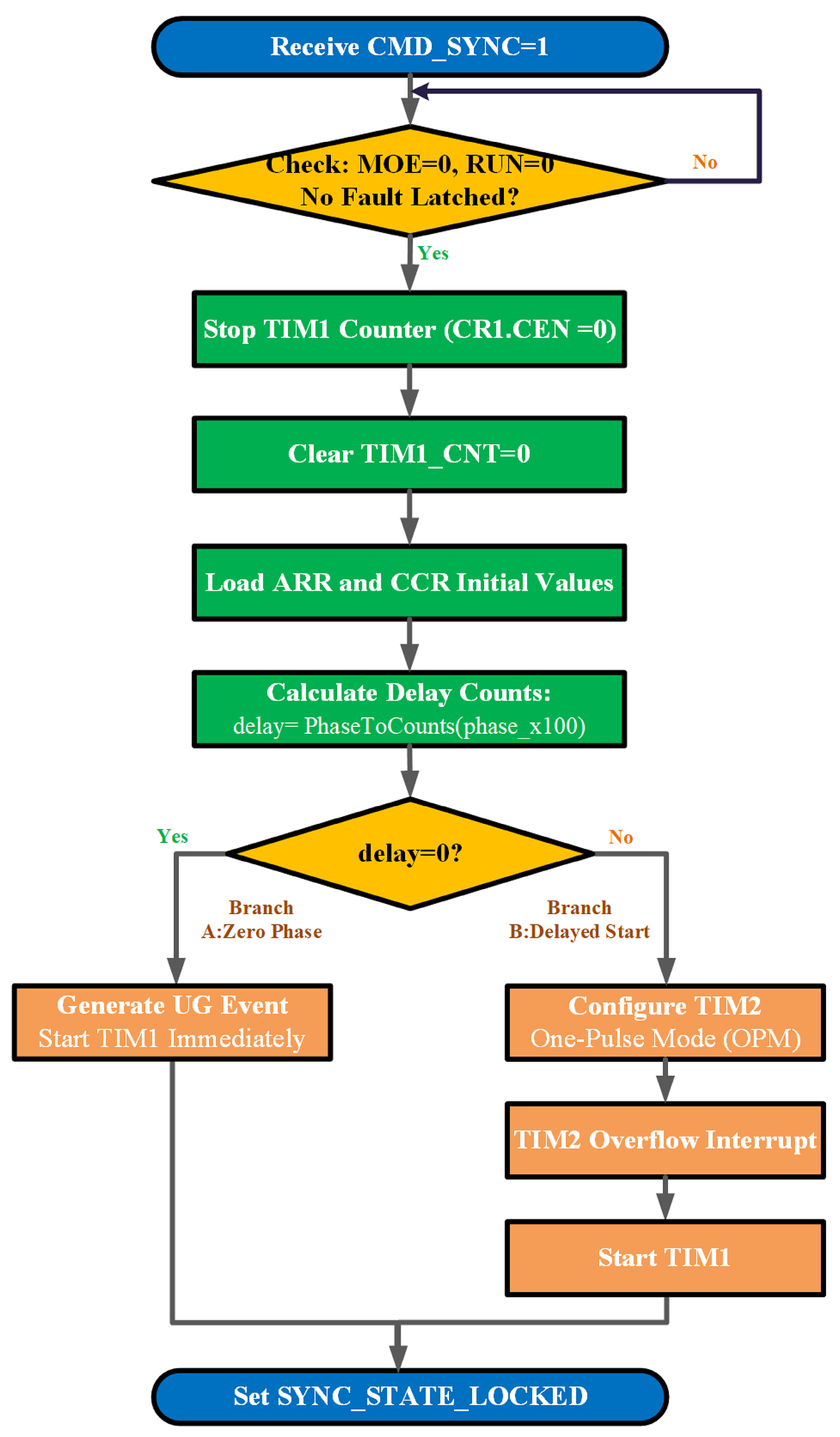
As shown in Figure 5, the execution flow is as follows: Upon receiving CMD_SYNC = 1, the system checks the above conditions, stops the TIM1 count (CR1.CEN = 0), clears TIM1_CNT, loads the initial values for ARR and CCR, and calculates the delay count. When the delay count reaches zero, an update event (UG) is immediately generated and TIM1 is started; when the delay count is greater than zero, TIM2 is configured for single-pulse mode with a delayed start, and TIM1 is started during the TIM2 expiration interrupt. After alignment is complete, the post-synchronization state is set to SYNC_STATE_LOCKED.
When the target counts offset Ntarget > 0, a delayed start is implemented using TIM2’s single-pulse mode. The automatic reload value for TIM2 is calculated according to Equation (16).
N TIM 2 = N target × f TIM 2 , CNT f TIM 3 , CNT
where NTIM2 is the TIM2 auto-reload value; Ntarget is the target count offset; fTIM2,CNT is the TIM2 count clock frequency (Hz); and fTIM3,CNT is the TIM3 count clock frequency (Hz). If the TIM2 clock is the same as the TIM3 clock (17.5 MHz), then as shown in Equation (17).
N TIM 2 = N target
TIM2 is configured for single-pulse mode (OPM); it automatically stops and generates an interrupt upon expiration, and TIM1 is started within the interrupt service routine. Since there is no power output at this time, resetting the count to zero does not affect the ongoing PWM waveform.

4.2. Soft Alignment: Run-Time Clipping Adjustment

Soft alignment follows these principles: do not directly reset the counter; do not suddenly jump by a full cycle; make small adjustments within the timer’s safe update window and gradually accumulate the adjustments until the phase returns to the target range [26,34].
A proportional limiting control law such as Equation (18) is adopted.
Δ A R R k = limit ( K p e k , Δ max , + Δ max )
where ΔARRk is the kth correction value, in counts; ek is the phase error, in counts; Kp is the proportional coefficient; and Δmax is the maximum correction value per iteration, in counts. In this paper, the values are taken as shown in Equation (19).
Δ max = 1
That is, at most one TIM1 count is corrected per carrier cycle.
The TIM1 counter clock is 35 MHz; the time corresponding to a single correction is given by Equation (20).
Δ t step = 1 35 × 10 6 28.57   ns
where Δtstep is the time interval between corrections, measured in nanoseconds (ns). Corrections are performed every 2 ms, and the correction rate is given by Equation (21).
ν correct = 28.57   ns 2   ms = 14.29   μ s / s
where vcorrect is the correction rate, measured in microseconds per second (μs/s). The convergence time is given by Equation (22).
t converge = | Δ t init | v correct
where tconverge is the convergence time, in seconds (s); Δtinit is the initial error, in microseconds (μs). The convergence times for soft alignment are shown in Table 9. When the initial error is 10 μs, the convergence time is 0.70 s; when the initial error is 20 μs, the convergence time is 1.40 s; when the initial error is 50 μs, the convergence time is 3.50 s; and when the initial error is 100 μs, the convergence time is 7.00 s.
A discrete-time model makes the convergence and noise limits explicit. Express the true phase-time error at carrier cycle k as ek (s), let q = 1/35 MHz = 28.57 ns be one TIM1 count, let d = Tcδrel be the per-cycle drift produced by relative frequency offset δrel, and let wk collect unmodeled drift. With measured error êk = ek + νk and dead band edz = 1 μs, the implemented law is uk = sgn(êk) when |êk| > edz and uk = 0 otherwise, with |uk| ≤ 1. The closed-loop model is ek+1 = ek + dquk + wk. In the noise-free case, strict convergence requires |d| < q, or |δrel| < q/Tc = 14.29 ppm. For |d| + wmax < q, a conservative settling bound is Ksettle ≤ ceil[(|e0| − edz)/(q − |d| − wmax)] carrier cycles. After entry into the dead band, bounded capture noise |νk| ≤ νmax gives |ek| ≤ edz + q + νmax; using the 100 ns capture-jitter allocation gives a 1.13 μs steady-state envelope. Table 9 evaluates e0 = 100 μs for several imposed relative offsets. The result is a parameterized numerical evaluation of the implemented update law, not a substitute for an oscillator-controlled hardware sweep. Offsets of 20 and 30 ppm exceed the available correction rate and produce residual drifts of 5.71 and 15.71 μs/s, respectively.
The same model can explicitly represent missing or rejected timing references. Let gk ∈ {0,1} denote reference validity at cycle k, where gk = 1 only when the frame/CRC and period checks are satisfied. The closed-loop update becomes ek+1 = ek + dkqgkuk + wk. Thus, a single invalid reference sets gk = 0 and freezes the correction action rather than injecting a spurious phase update; consecutive invalid references are then handled by the state-machine thresholds in Table 10. This separation is useful because the numerical convergence condition concerns the valid-reference soft-alignment loop, whereas communication-loss protection is governed by deterministic counters and the transition to SYNC_STATE_LOST.
To avoid carrier frequency jitter caused by repeated adjustments near zero, a dead zone is set as shown in Equation (23).
N dz = 35   counts 1.0   μ s 0.18 ( f timer = 35   MHz ,   f c = 500   Hz )
where Ndz is the dead-band count, ftimer is the TIM1 counter frequency, and fc is the carrier frequency defined previously. Errors within the dead band are not corrected. The correction is applied to the ARR register during the TIM1 update interrupt, is valid only for the current cycle, and reverts to its nominal value in the next cycle [27].

4.3. Synchronous State Machines and Desynchronization Criteria

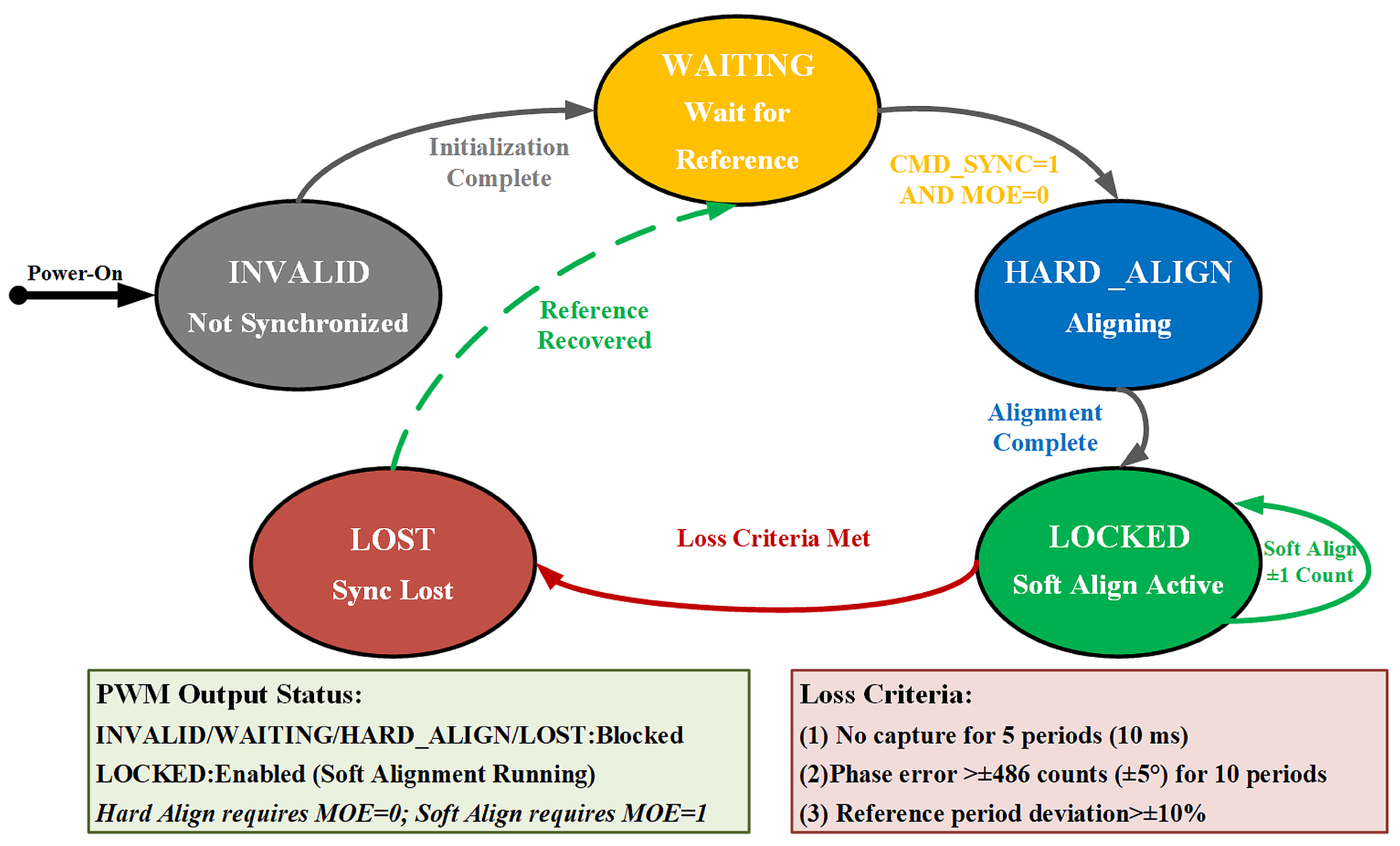
There are five defined synchronization states: SYNC_STATE_INVALID (invalid, not synchronized); SYNC_STATE_WAITING (waiting for reference signal); SYNC_STATE_HARD_ALIGN (hard alignment in progress); SYNC_STATE_LOCKED (locked, soft alignment maintained); and SYNC_STATE_LOST (out of sync).
As shown in Figure 6, the state transition relationships are as follows: INVALID transitions to WAITING after initialization is complete; WAITING transitions to HARD_ALIGN upon receiving CMD_SYNC and when MOE = 0; HARD_ALIGN transitions to LOCKED after alignment is complete; LOCKED transitions to LOST when the desynchronization criterion is met; and LOST transitions to WAITING after the reference is restored.
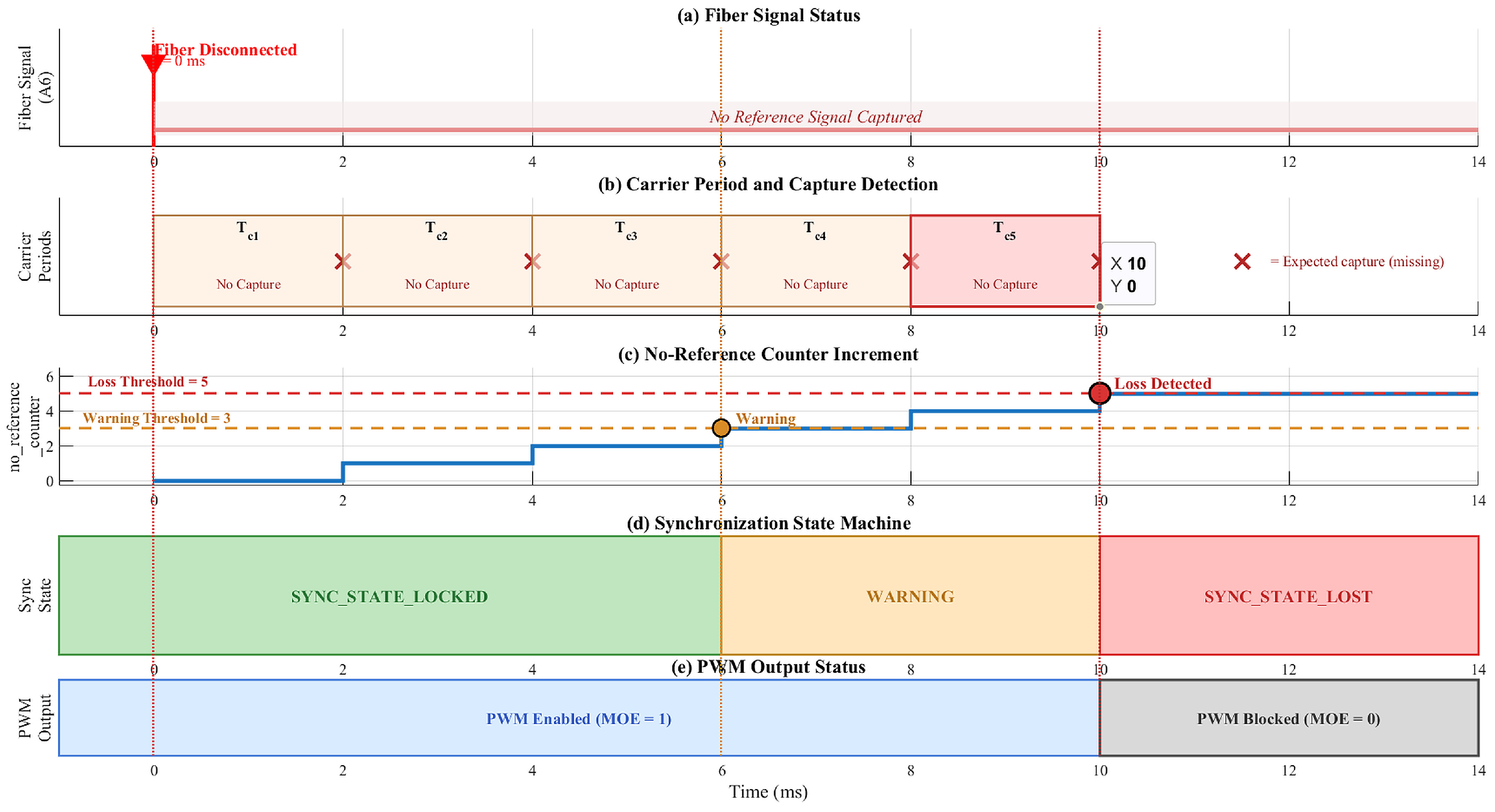
Table 10 consolidates the implemented response to missing, corrupted, or temporally implausible references. A frame is valid only when the frame/CRC checks and the reference-period check pass. One or two consecutive invalid references hold the previous alignment action without alarming. Three consecutive invalid references (6 ms) set the synchronization alarm; five (10 ms) enter SYNC_STATE_LOST and disable PWM. A phase error beyond ±5° for 10 cycles also causes loss of synchronization. Narrow or off-period edges are rejected by the TIM3 filter and the ±10% period window and are counted as invalid references only after frame validation.
In particular, the count value corresponding to ±5° is given by Equation (24).
N 5 = 5 360 × N period = 5 360 × 35000 486
where N 5 is the count corresponding to a phase error of 5°, and Nperiod is the carrier-period count defined in Equation (10).
The permissible range of the reference period is determined according to Equations (25) and (26).
N period , min = 0.9 × 35000 = 31500
N period , max = 1.1 × 35000 = 38500
where Nperiod,min and Nperiod,max represent the lower and upper limits, respectively, of the reference period count. The interval between two consecutive valid captures must fall within this range; if it exceeds this range, the capture is deemed invalid and is not used in the phase error calculation.
After synchronization loss, PWM remains disabled and ST_SYNC_LOST is reported. Reappearance of a valid frame returns the state machine to WAITING, but PWM is not resumed from the previous counter state. A valid CMD_SYNC frame with MOE = 0 is required to execute hard alignment and return to LOCKED. This fail-silent sequence prevents repeated corrupted or intermittently restored frames from causing uncontrolled automatic restart.

5. Error-Budget Analysis and Performance Comparison

5.1. Decomposition of Sources of Error

The error budget separates systematic differential offsets, random jitter allocations, timer quantization, and algorithmic bounds. A delay common to every cell does not change relative carrier phase and is excluded. Table 11 now distinguishes three evidence levels for every entry: clock- or geometry-derived values, component-specification/engineering allocations, and end-to-end measurements. Except for timer resolution and configured algorithmic thresholds, the individual physical contributions were not de-embedded experimentally; this limitation is stated explicitly rather than inferred from the aggregate result.
The 100 ns fiber term follows from the maximum 20 m path-length difference at approximately 5 ns/m. The 500 ns optical-module and 200 ns shaping-input-path terms are conservative unit-to-unit spread allocations; PCB trace and connector skew are included in the latter because they were not measured separately. The 57 ns TIM3 value follows exactly from the 17.5 MHz capture clock. The 1 μs term is the configured soft-alignment dead band. The last 500 ns value is a residual oscillator-related allocation associated with the component tolerance and is not the per-cycle drift. FPGA launch jitter and capture jitter retain 100 ns allocations because no independent channel-resolved records are available.
Δ t res = 1 f TIM 3 , CNT = 1 17.5 × 10 6 57   ns
The capture resolution is Δtres = 1/fTIM3,CNT ≈ 57 ns, as given by Equation (27). All remaining component entries and their evidence status are listed in Table 11. In particular, the ±30 ppm component tolerance is not the implemented convergence range, and an unmeasured allocation must not be described as a measured contribution.
For a guaranteed implementation bound, the magnitudes of the eight nonoverlapping allocated terms are added linearly, as shown in Equation (28). PCB/connector skew is contained within the shaping-input-path allocation and is not added a second time. This conservative construction gives Δtsync,max < 2.56 μs.
Δ t sync , max = i = 1 8 Δ t i < 2.56   μ s , Δ ϕ err , max < 0.46
where Δtsync,max is the worst-case cumulative synchronization error and Δti is the magnitude assigned to the i-th nonoverlapping source. Equation (29) is reported only as an engineering estimate: root-sum-square combination requires approximately independent, zero-mean signed contributions after common delays are removed and is not a guaranteed bound.
Δ t sync , rms = i = 1 8 Δ t i 2 < 1.28   μ s ,   Δ ϕ err , rms < 0.23
The root-sum-square estimate is 1.28 μs (0.23°). The measured end-to-end RMS of the 11 Phase-A offsets in Table 12 is 1.22 μs (0.22°), the maximum is 2.00 μs (0.36°), and the coarse eight-hour record has a standard deviation of 0.85 μs (0.153°). These aggregate values are consistent with the budget scale and remain below its 2.56 μs linear bound. They do not identify the individual contributions, validate their independence, or constitute a theoretical-versus-measured match for each row.
The theoretical-versus-measured comparison must also distinguish spatial phase-offset statistics from temporal jitter. The measured 2.00 μs maximum spatial offset is 78.1% of the 2.56 μs conservative linear budget, while the 1.22 μs spatial RMS is 95.3% of the 1.28 μs RSS engineering estimate. The latter numerical proximity is reported only as a scale check: it does not validate statistical independence of the individual budget terms and it must not be interpreted as a cycle-to-cycle jitter measurement. Table 11 therefore provides an error-budget audit trail rather than a parameter-identification result.

5.2. Evidence-Controlled Baseline Comparison with the Traditional EXTI Method

For the pre-modification EXTI path, the 2–10 μs software-latency range is an estimate from the code path, interrupt pre-emption, and device timing rather than a controlled measurement on the present prototype. Adding the remaining bounded terms gives an analytical worst-case total above 6 μs, corresponding to more than 1.08° at 500 Hz. Table 12 therefore remains an analytical baseline only.
Table 12. Analytical error estimate for the EXTI scheme.
Analytical Error TermTypical ValueTime Error Phase Error
EXTI-response latency2–5 μs typical; up to 10 μs2–10 μs0.36–1.80°
Other bounded terms (Table 11, items 1–4 and 7–8)<1.46 μs0.26°
Analytical worst-case total>6 μs>1.08°
For the TIM3 path, the reference instant is latched by the capture peripheral and interrupt-entry latency is excluded from the timestamp. Table 13 now reports every metric requested for an identical-platform comparison and labels it as measured, analytical, or unavailable. Because the EXTI path was not reimplemented during the available prototype test window, RMS error, maximum error, short-term jitter, CPU utilization, and long-term stability are not reported for EXTI, and no measured improvement factor is claimed.
Accordingly, Table 13 is a direct method-level baseline comparison but not a same-run experimental A/B comparison. The EXTI column represents the traditional interrupt-based implementation on the same controller architecture and is bounded from the software path and device timing; the TIM3 column contains the measurements actually retained from the modified prototype. This evidence separation is deliberate: the manuscript does not convert the 2–10 μs EXTI latency estimate into an artificial measured RMS or peak-to-peak value, and no experimental improvement ratio is claimed where the required baseline record is unavailable.
The hardware modification requires only shorting the three pins (PA6, PA7, and PA12); no additional components or optical fibers are required.

5.3. Comparison with Conventional Methods

Table 14 shows a comparison of this approach with four conventional methods: centralized PWM, dedicated SYNC line, frame-header EXTI, and pure distributed phase-locked loop.
The proposed scheme is less accurate than a dedicated synchronization link but halves the fiber count and preserves cell interchangeability. Relative to frame-header EXTI acquisition, only the analytical worst-case bounds indicate an improvement. Table 13 prevents this analytical difference from being interpreted as a same-platform experimental result and identifies the missing A/B metrics explicitly.
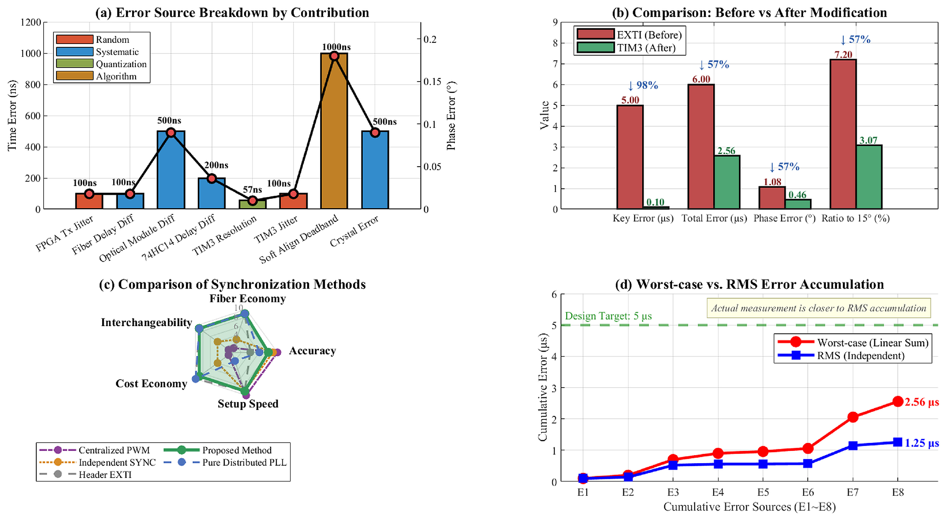
Figure 7 shows the error budget analysis and the results of the improvements.
Figure 7a error source decomposition: Among the eight error sources, the soft-alignment dead zone (1000 ns) and individual variations in optical modules (500 ns) are the primary contributors, encompassing the four types of error: random, systematic, quantization, and algorithmic.
Figure 7b visualizes the analytical budget comparison: replacing software timestamping with TIM3 input capture lowers the estimated worst-case timing and phase error bounds by approximately 57%. The figure does not represent measured EXTI/TIM3 RMS error, jitter, CPU load, or long-term stability; those evidence categories are separated in Table 13.
Figure 7c Comprehensive Comparison of the Five Schemes: This scheme (green solid line) exhibits a relatively balanced distribution across the five dimensions of accuracy, fiber-optic cost-effectiveness, cell interchangeability, hardware cost-effectiveness, and setup speed, making it an engineering compromise across all metrics.
Figure 7d compares the two combination rules. Linear addition gives the guaranteed conservative bound of 2.56 μs; root-sum-square combination gives an engineering estimate of 1.28 μs under independence and zero-mean assumptions. The measured RMS value of 1.22 μs for the proposed scheme is close to the latter, but no inference is made about the unmeasured EXTI baseline.
The proposed method is intended for systems with more than 10 power cells, constrained fiber capacity, interchangeable cells, an existing communication link, and a synchronization requirement in the 1–5 μs range. A dedicated synchronization link remains preferable below 500 ns, whereas centralized PWM is simpler for fewer than five cells. The proposed architecture is therefore an engineering compromise for medium- and high-voltage CHB converters.

6. Experimental Validation

6.1. Experimental Platform

The experimental hardware is a 13.8 kV, 3 MW, 36-cell cascaded H-bridge soft-starter prototype with 12 cells per phase. The rating describes the prototype design; it does not mean that every test reported below was performed at 13.8 kV and 3 MW. The complete 36-cell controller and optical-link hardware was used for the timing, synchronization-loss, recovery, and long-duration tests at fc = 500 Hz. The single-phase cascaded-output waveform and FFT measurements were performed at 380 V. No full-power 13.8 kV/3 MW loaded waveform or EMC test is included in this study.
The test matrix comprises inter-cell phase-offset measurements, a 12-cell 380 V cascaded-output waveform and spectrum, a manual A6 fiber-interruption/recovery test, and an eight-hour coarse-sampled drift record. No controlled EXTI/TIM3 A/B test, oscillator-mismatch sweep, corrupted-frame injection campaign, active-layer-count sweep, cycle-resolved jitter acquisition, or full-voltage EMC test is included. The analytical and state-machine evaluations added in this revision are labeled separately from measured evidence.
The validation evidence is therefore classified by bandwidth and provenance. Table 15 is a spatial accuracy test across cells, Figure 8 is a low-bandwidth drift record, and Figure 9 is a single physical link-interruption/recovery test. None of these records contains continuous per-carrier-cycle timestamps. Because such information cannot be reconstructed from the archived figures without inventing data, cycle-resolved short-term jitter is reported as unavailable rather than estimated from the 600 s drift samples.

6.2. Static Inter-Cell Carrier-Phase Accuracy Measurement

A dual-channel oscilloscope was used to observe simultaneously the PWM rising edges at PA8 (TIM1_CH1) of adjacent Phase-A cells A1 and A2. The theoretical interval is 83.333 μs, corresponding to 15° at fc = 500 Hz. Figure 8 shows the measured waveforms.
Figure 8. Adjacent unit PWM waveforms (A1 and A2); the PWM ordinate is a dimensionless logic level (0/1), and the abscissa is time in microseconds (μs).
Energies 19 04440 g008
Using A1 as the reference, the time offsets of A2 through A12 relative to A1 were measured in sequence; the measured data are shown in Table 16. The phase angles were calculated from the time offsets as shown in Equation (30).
ϕ measured = Δ t measured T c × 360
where φmeasured is the measured phase angle in degrees (°), Δtmeasured is the measured time offset in microseconds (μs), and Tc is the 2000 μs carrier period defined previously. Table 16 reports the measured phase data for Phase-A cells relative to A1.
The maximum absolute phase-offset deviation is 0.36° at A4, A7, and A10. Using the 11 deviations listed in Table 16, the root-mean-square deviation is calculated by Equation (31).
σ φ = 1 N i = 1 N ε i 2 = 0.22
where σφ is the RMS phase deviation, εi is the ith measured deviation, and M = 11 is the number of deviations. Direct substitution of the Table 16 data gives σφ = 0.223°, reported as 0.22° after rounding. The maximum deviation of 0.36° is 2.4% of the 15° designed phase shift, and both statistics satisfy the criterion Δtsync < 5 μs (Δφerr < 0.9°).
These 11 values quantify cell-to-cell static phase-placement accuracy at the measured operating point. They do not constitute 11 temporal samples of one cell pair and therefore are not used to infer short-term jitter, peak-to-peak timing noise, or a jitter probability distribution.

6.3. Low-Voltage Cascaded-Output Waveform

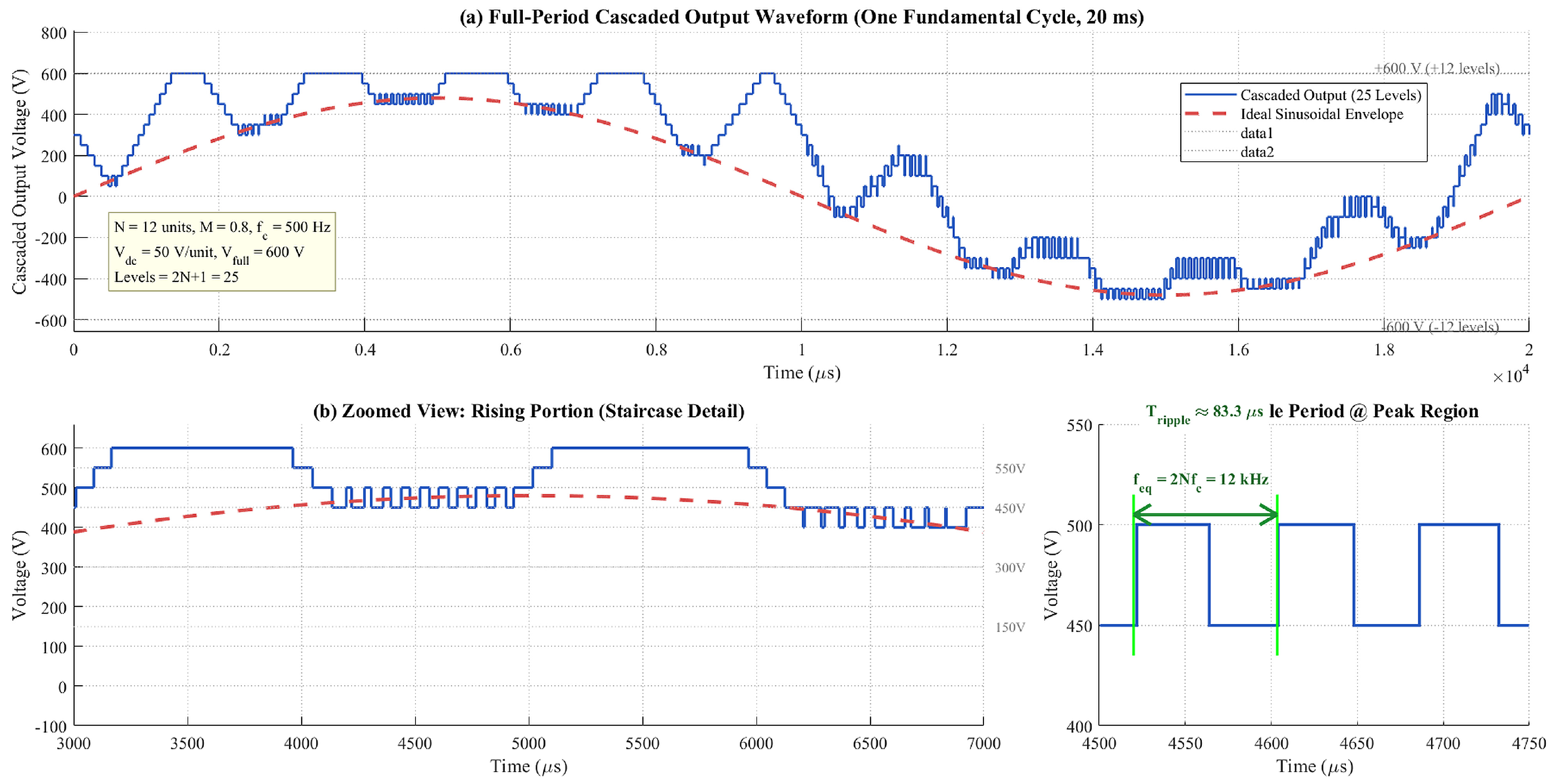
To evaluate cascaded-output quality, the single-phase 12-cell output was tested at 380 V on the grid side, with modulation index M = 0.8 and carrier frequency fc = 500 Hz. This is a low-voltage functional test rather than a rated 13.8 kV/3 MW test. The measured waveform in Figure 9 is a 25-level staircase with a sinusoidal envelope and a dominant ripple near 12 kHz.
Figure 9. Measured single-phase 12-unit cascaded-output waveform.
Energies 19 04440 g009
Figure 9 presents the measured results of a single-phase 12-cell cascaded output from three perspectives: the full-cycle waveform, a magnified view of a local step, and the ripple period in the peak region. The full-cycle waveform shows that the output is a 25-level step wave, consistent with the theoretical number of levels, 2N + 1 = 25, and the sine envelope is smooth; in the magnified view, the widths of each level are generally uniform, with no obvious level missing, repetition, or transition phenomena observed; and the ripple period in the peak region is approximately 83.3 μs, corresponding to an equivalent switching frequency of 12 kHz, which aligns with the theoretical value feq = 2Nfc. The test results indicate that the phase relationships among the carrier waves of each unit meet expectations, and the harmonic cancellation and level superposition effects of CPS-SPWM satisfy the design requirements.

6.4. Spectrum Analysis

An FFT was applied to the 380 V single-phase cascaded-output voltage over 0–20 kHz. Table 17 lists the measured components relative to the 50 Hz fundamental.
Figure 10 shows the FFT spectrum analysis results for the cascaded-output voltage. Figure 10a displays the full spectrum from 0 to 20 kHz, with the majority of the energy concentrated at two frequency points: the 50 Hz fundamental and the 12 kHz main ripple; all other frequency components are below the −40 dB suppression reference line. Figure 10b zooms in on the low-frequency band (2 kHz); the amplitudes of both the 500 Hz carrier sideband and the 1 kHz carrier second-harmonic sideband are below −42 dB, indicating that CPS-SPWM effectively cancels out the unit carrier-frequency components. Figure 10c shows a magnified view of the main ripple region (10–15 kHz); the measured main ripple frequency matches feq = 2N × fc = 2(12) × (500 Hz) = 12 kHz. The spectral analysis results are consistent with the expected harmonic cancellation characteristics of CPS-SPWM, further validating the intended inter-cell carrier phase shifts under the 380 V test condition.

6.5. Loss-of-Synchronization and Recovery Test

The only physical communication-disturbance experiment available for this revision was a manual interruption of the A6 downstream fiber, shown in Figure 11. At t = 0 ms the fiber was disconnected; after three missing valid references the alarm asserted at 6 ms, and after five missing references the controller entered SYNC_STATE_LOST and disabled PWM at 10 ms. Corrupted-frame, short-pulse, and intermittent-loss cases were evaluated against the implemented validation logic in Table 10 but were not separately injected and measured.
Figure 11 confirms the measured missing-reference sequence for A6: the counter reaches the alarm threshold at 6 ms and the loss threshold at 10 ms, after which MOE is cleared and ST_SYNC_LOST is reported. The same deterministic counters apply to consecutive CRC-invalid or period-invalid frames because they do not produce a valid reference update; this is an implementation-level result, not an additional disturbance measurement.
After the A6 fiber was reconnected, a valid frame returned the unit to WAITING, CMD_SYNC = 1 initiated hard alignment, and LOCKED status was reported before the DSP restored system readiness. The measured end-to-end recovery time was below 2 s; this value includes command scheduling and status reporting and is not the hard-alignment pulse width. Under repeated failures the controller remains in LOST and does not re-enable PWM until a valid hard-alignment sequence is completed.
For brief communication disturbances, the implemented behavior is deterministic even though only the complete A6 interruption was physically injected in this revision. One or two consecutive invalid references (<6 ms) retain the previous alignment action without an alarm; three invalid references assert the synchronization alarm at 6 ms; five invalid references force the fail-silent LOST state and PWM blocking at 10 ms. Recovery from LOST is intentionally non-autonomous: a valid link first returns the unit to WAITING, after which a CMD_SYNC hard-alignment sequence is required before PWM can be re-enabled. This prevents burst errors or intermittent reconnection from causing an uncontrolled restart.

6.6. Coarse-Sampled Long-Term Drift Test and Resolution Limits

The complete 36-cell synchronization hardware operated for 8 h at fc = 500 Hz under the low-voltage test supply. The A7-to-A1 phase offset was recorded once every 600 s, yielding 48 points. This corresponds to a sampling frequency of 1.667 mHz and a Nyquist frequency of only 0.833 mHz. The maximum, minimum, mean, and standard deviation shown by the retained 48-point record are +0.328°, −0.257°, +0.064°, and 0.153° (0.85 μs), respectively. These statistics and Table 18 have been reconciled to the values embedded in Figure 12; because the archived log values are available only through this coarse record, no finer effective reporting resolution is inferred.
Figure 12 shows no systematic trend in the 48 coarse samples, so it supports long-term drift stability under the laboratory condition. It cannot resolve cycle-to-cycle jitter, instantaneous peak-to-peak error, or a broadband statistical distribution. Those quantities require a continuous timestamped capture stream or oscilloscope histogram with stated analog bandwidth and trigger resolution, neither of which was preserved in the available data set. Accordingly, the terms ‘instantaneous jitter’ and ‘jitter distribution’ are not inferred from Figure 12.
To obtain the higher-resolution short-term statistics requested for a future same-platform test, the capture register should be logged continuously at the 2 ms carrier rate (500 samples/s per monitored pair) for both EXTI and TIM3 paths under identical interrupt load, temperature, supply, and EMI conditions. The minimum report should include sample count and duration, timestamp resolution, RMS/standard deviation, maximum absolute error, peak-to-peak jitter, percentile limits, histogram or empirical CDF, and the measurement bandwidth. This protocol is stated here so that coarse drift stability and high-bandwidth jitter are not conflated.
Taken together, the measured tests verify inter-cell timing accuracy at selected points, fail-silent response to one fiber interruption, recovery logic, and 380 V waveform/spectral behavior. The eight-hour record verifies only low-frequency drift at the stated sampling resolution. Cycle-resolved jitter, multiple communication-fault modes, variable active-cell counts, a same-platform EXTI comparison, and full-voltage EMC immunity remain outside the measured evidence.


7. Conclusions and Discussion

7.1. Conclusions

To meet the engineering requirement of carrier synchronization among multiple power cells in CHB high-voltage drives under CPS-SPWM control, this paper has proposed a carrier synchronization method that multiplexes the communication data link with the synchronization reference. The main work and conclusions are summarized as follows.
(1)
A phasor-based bound has been established between synchronization error and the residual of carrier groups that ideally cancel. For fc = 500 Hz, the 5 μs design limit corresponds to 0.90° and bounds the normalized residual of the second canceled carrier group by −30.1 dB. The limit is therefore a conservative engineering criterion; the measured 380 V operating point lies within it, but the boundary itself was not experimentally swept.
(2)
The communication link and synchronization reference are multiplexed so that the 36-cell system requires no dedicated synchronization fibers. Relative to a separate synchronization-link architecture, the fiber and transceiver counts are reduced by 50%. Relative to frame-header EXTI acquisition, the error budget predicts a lower timing bound; no same-platform experimental improvement factor is claimed. The scheme retains a unified firmware image, cell interchangeability, and dynamic configuration of 5–12 cascaded layers.
(3)
Hardware timer input capture removes software interrupt-response latency from the timestamp path. The worst-case analytical budget is below 2.56 μs (0.46°), compared with an estimated EXTI bound above 6 μs (1.08°). These values quantify an analytical comparison; the measured result for the proposed scheme is reported separately. The modification requires only three pin-to-pin connections and no printed-circuit-board redesign.
(4)
Standstill hard alignment establishes the counter origin, and on-line soft alignment limits each correction to one 28.57 ns timer count per 2 ms carrier period. The corresponding correction capacity is 14.29 μs/s; therefore, the implemented configuration has the strict convergence condition |δrel| < 14.29 ppm. The ±30 ppm component tolerance used in the oscillator-related budget is not the guaranteed convergence range.
(5)
For the proposed scheme, the measured RMS inter-cell phase deviation is 0.22° (1.22 μs) and the maximum is 0.36° (2.00 μs). The 380 V, 12-cell output has the expected 12 kHz dominant ripple, while the 500 Hz and 1 kHz sidebands remain below −42 dB. Missing-reference protection disables PWM within 10 ms and measured recovery is below 2 s. The 48-point, eight-hour record shows no low-frequency drift trend, but it is not a cycle-resolved jitter measurement.
Table 19 places the measured result in the context of representative recent approaches and adds the comparison dimensions requested for engineering selection: synchronization accuracy and evidence type, hardware/fiber requirements, synchronization time, scalability, and computational burden. Literature-reported values are not converted into same-platform measurements.
The comparison shows that the proposed scheme does not target nanosecond or sub-microsecond applications in which a second fiber, timestamp-capable bidirectional network, or additional feedback is acceptable. Its demonstrated advantage is a 0.22° (1.22 μs) spatial RMS phase-offset deviation and a 0.36° (2.00 μs) maximum spatial deviation on a 36-cell controller while using the existing unidirectional downlinks, one hardware capture, one modular subtraction, validity comparisons, and at most one timer-count correction per 2 ms cycle. Per-cell execution remains O(1), whereas master-side fan-out and the number of fibers grow linearly with cell count. The architecture supports parameterized phase targets, but the reported hardware test used 12 active cells per phase; scalability to other active-cell counts is supported by the architecture and generalized criterion, not by an experimental sweep.
Without increasing the number of optical fibers, and at the hardware cost of shorting three pins, the proposed method raises the carrier synchronization accuracy of the power cells to a level that satisfies the harmonic cancellation requirement of CPS-SPWM, providing a practical synchronization solution for engineering applications of medium-voltage high-power cascaded converters.

7.2. Discussion

Several aspects of the proposed method merit further investigation for engineering application.
(1)
On-line calibration and compensation of individual device variations. In the error budget, the unit-to-unit variation in the propagation delay of the optical transceivers (500 ns) and that of the pulse-shaping circuits (200 ns) constitute the dominant part of the residual error. It should be noted that any fixed delay common to all cells acts as a common-mode component and does not affect the relative phase shift between cells; only the individual variation enters the phase error. The present scheme suppresses this variation by controlling the consistency of device batches, but it cannot be eliminated entirely, and the 500 ns estimate is taken from the delay distribution range given in the device datasheet rather than from per-cell measurement statistics. Future work may address on-line measurement and compensation of the intrinsic delays of the optical transceivers and shaping circuits. If per-cell calibration is adopted, a trade-off arises between the storage location of the calibration parameters and the interchangeability of power cells; one possibility is to store the calibration table centrally at the master controller and download it to each cell at power-up.
(2)
Soft-alignment operating range and adaptation. The implemented one-count-per-period limit gives a 14.29 μs/s correction rate and therefore requires |δrel| < 14.29 ppm. The eight-hour result confirms that the tested clocks remained within the correctable range, but operation over the full ±30 ppm component population is not guaranteed without screening or calibration. Increasing the rate limit adaptively or estimating relative clock frequency on-line could extend the operating envelope while preserving output continuity [35,36,37].
(3)
Extension to different active-cell counts and carrier frequencies. The synchronization hardware has been tested with 36 installed cells and 12 active cells per phase at fc = 500 Hz. Changing the active-cell count changes the commanded phase spacing and Ntarget but not the O (1) capture calculation in each cell. Nevertheless, no 5-to-12 active-layer sweep or test beyond 12 active cells per phase is included, so scalability is claimed only at the architectural level. The generalized rule in Section 2.3 shows that a larger N or fc can tighten the time-error requirement; for example, the 6%-of-spacing constraint is 3.33 μs for N = 18 at 500 Hz and 2.50 μs for N = 12 at 1 kHz. A new harmonic mask and modulation-dependent coefficient must also be evaluated when M changes.
(4)
Communication reliability and fault coverage. Multiplexing timing and control on one link means that interruption removes both functions. The measured A6 disconnection verifies the 6 ms alarm, 10 ms PWM blocking, and below-2 s end-to-end recovery sequence. CRC-invalid frames, implausible periods, short pulses, repeated failures, and temporary interruptions shorter than three frames are covered by the deterministic logic summarized in Table 10, but they were not separately fault-injected in the reported campaign. Claims of experimental robustness are therefore limited to the single interruption/recovery case.
(5)
Immunity in strong electromagnetic environments. Optical transmission provides galvanic isolation and is not susceptible to conducted interference along the fiber, but the photoreceiver, 74HC14 shaping stage, supply/ground network, and parallel timer-input node remain electrical EMI entry points. The present design combines the Schmitt trigger, TIM3 digital filtering, CMD_SYNC/CRC validation, and reference-period plausibility checks. No false capture was observed during the eight-hour low-voltage test; however, this does not constitute rated-voltage EMC qualification. Conducted and radiated immunity tests during 13.8 kV switching are required to establish the full-voltage margin and determine whether additional filtering or dual-edge validation is necessary.
(6)
Experimental comparison and higher-bandwidth timing statistics. The archived prototype data do not contain a same-platform EXTI/TIM3 A/B record or cycle-resolved capture timestamps. Consequently, the EXTI comparison is restricted to the analytical latency/error budget in Table 12 and Table 13, and the eight-hour record is explicitly described as a coarse drift measurement rather than a jitter measurement. A definitive follow-up experiment should implement both acquisition paths on the same controller and acquire continuous 2 ms-cycle timestamps under matched interrupt load, temperature, supply, and EMI conditions, reporting RMS, maximum, peak-to-peak, percentile/distribution, measurement bandwidth, CPU utilization, synchronization-loss probability, and recovery-time statistics. This limitation is retained explicitly to avoid overstating experimental evidence.
Author Contributions

Conceptualization, W.L., Z.H., and J.T.; methodology, W.L., C.P., and C.Y.; visualization, W.L., C.P., C.W.; writing (original draft preparation), W.L., Z.H., and T.W.; writing (review and editing), W.L., J.T., and C.P.; validation, C.Y. and T.W.; supervision, C.W. All authors have read and agreed to the published version of the manuscript.

Funding

This work was supported by the Science and Technology Department of Hubei Province, China (2024BAB067) and 2025 Chutian Elite Program for Innovation and Entrepreneurship Teams (20259109).

Data Availability Statement

The original contributions presented in this study are included in the article. Further inquiries can be directed to the corresponding author.

Acknowledgments

We are grateful to our families, friends, and laboratory colleagues for their unwavering understanding and encouragement.

Conflicts of Interest

Author Jiatao Tao was employed by Hubei Zhongsheng Electric Co., Ltd. The remaining authors declare that the research was conducted in the absence of any commercial or financial relationships that could be construed as a potential conflict of interest.

References

  1. Ondin, U.; Balikci, A. A Transformer Design for High-Voltage Application Using LLC Resonant Converter. Energies 2023, 16, 1377. [Google Scholar] [CrossRef] [Scilit]
  2. Cai, K.; Xiao, J.; Yang, Z.; Hu, R. Three-Level All-SiC High-Frequency High-Voltage Plasma Power Supply System. Energies 2025, 18, 1617. [Google Scholar] [CrossRef] [Scilit]
  3. Choudhury, S.; Bajaj, M.; Dash, T.; Kamel, S.; Jurado, F. Multilevel Inverter: A Survey on Classical and Advanced Topologies, Control Schemes, Applications to Power System and Future Prospects. Energies 2021, 14, 5773. [Google Scholar] [CrossRef] [Scilit]
  4. Salem, M.; Richelli, A.; Yahya, K.; Hamidi, M.N.; Ang, T.-Z.; Alhamrouni, I. A Comprehensive Review on Multilevel Inverters for Grid-Tied System Applications. Energies 2022, 15, 6315. [Google Scholar] [CrossRef] [Scilit]
  5. Guo, A.; Tian, Y.; Zhao, H. Highly Robust Active Damping Approach for Grid-Connected Current Feedback Using Phase-Lead Compensation. Electronics 2025, 14, 309. [Google Scholar] [CrossRef] [Scilit]
  6. Soares, L.T.F.; Souza, A.C.; Silva, W.; Rezende, G.M.d.; Brandao, D.I. Battery Energy Storage System for Grid Frequency Support Using the Virtual Synchronous Machine Strategy. Energies 2026, 19, 3015. [Google Scholar] [CrossRef] [Scilit]
  7. Yan, B.; Huang, H.; Wang, H. Robust phase-shifted model predictive control for cascaded H-bridge power supplies using linear matrix inequality. J. Power Electron. 2022, 22, 1496–1507. [Google Scholar] [CrossRef] [Scilit]
  8. Li, Z.; Li, J. Comprehensive Evaluation and Optimization of Level Count for Cascaded H-Bridge Multilevel Inverters with Carrier-Phase-Shifted PWM. Machines 2026, 14, 628. [Google Scholar] [CrossRef] [Scilit]
  9. Luo, D.; Lin, D.; Zhang, W.; Lian, W. A Novel Jittered-Carrier Phase-Shifted Sine Pulse Width Modulation for Cascaded H-Bridge Converter. J. Eng. 2024, 2024, e12391. [Google Scholar] [CrossRef] [Scilit]
  10. Hakami, S.S.; Halabi, L.M.; Lee, K.B. High Efficiency and Low Complexity Dual-Reference Voltage-Based Pulse Width Modulation for Three-Phase Five-Level HANPC Inverters. J. Electr. Eng. Technol. 2024, 19, 3047–3057. [Google Scholar] [CrossRef] [Scilit]
  11. Huang, H.; Zheng, X.; Wu, Y.; Sheng, Z. Design of High Precision and High Power Bidirectional Adjustable Power Supply. Fusion Eng. Des. 2021, 162, 112103. [Google Scholar] [CrossRef] [Scilit]
  12. Chang, Y.-H.; Wu, T.-F.; Chiu, J.-Y.; Hung, C.-C. Grid Simulator with Phase-Amplitude Compensation. IEEE Trans. Ind. Appl. 2024, 60, 4201–4212. [Google Scholar] [CrossRef] [Scilit]
  13. Govind, S.; Chappa, A.; Rao, K.D.; Dawn, S.; Ustun, T.S. Development of an Enhanced Selective Harmonic Elimination for a Single-Phase Multilevel Inverter with Staircase Modulation. Electronics 2022, 11, 3902. [Google Scholar] [CrossRef] [Scilit]
  14. Vijayakumar, A.; Stonier, A.A.; Peter, G.; Loganathan, A.K.; Ganji, V. Power Quality Enhancement in Asymmetrical Cascaded Multilevel Inverter Using Modified Carrier Level Shifted Pulse Width Modulation Approach. IET Power Electron. 2022, 19, e12429. [Google Scholar] [CrossRef] [Scilit]
  15. Jiao, N.; Wang, S.; Ma, J.; Chen, X.; Liu, T.; Zhou, D.; Yang, Y. The closed-loop sideband harmonic suppression for CHB inverter with unbalanced operation. IEEE Trans. Power Electron. 2022, 37, 5333–5341. [Google Scholar] [CrossRef] [Scilit]
  16. Chen, Y.; Song, S.; Liao, Z.; Luo, D.; Lin, D.; Wei, D. A new carrier phase-shift modulation based on switching the displacement angle. Energies 2022, 15, 7954. [Google Scholar] [CrossRef] [Scilit]
  17. Koyama, Y.; Isobe, T. Current Control of Modular Multilevel Converters with Phase-Shifted PWM Using a Daisy-Chained Distributed Control System. IEEJ Trans. Electr. Electron. Eng. 2019, 14, 1095–1104. [Google Scholar] [CrossRef] [Scilit]
  18. Guo, X.; Liu, B.; Kong, W.; Quan, H.; Zhang, Y.; Liu, T.; Dong, R.; Zhang, S. A high-precision bidirectional time-transfer system over a single fiber based on wavelength-division multiplexing and time-division multiplexing. Front. Phys. 2023, 10, 1080966. [Google Scholar] [CrossRef] [Scilit]
  19. Manduchi, G. Overlaps between industrial informatics and control, data acquisition and management in Big Science. Front. Ind. Eng. 2024, 2, 1342734. [Google Scholar] [CrossRef] [Scilit]
  20. Chicco, G. Data consistency for data-driven smart energy assessment. Front. Big Data 2021, 4, 683682. [Google Scholar] [CrossRef] [Scilit] [PubMed]
  21. Avraham, Y.; Pinchas, M. Performance of the modified clock skew estimator and its upper bound for the IEEE 1588v2 (PTP) case under packet loss and fractional Gaussian noise environment. Front. Phys. 2023, 11, 1222735. [Google Scholar] [CrossRef] [Scilit]
  22. Idrees, Z.; Granados, J.; Sun, Y.; Latif, S.; Gong, L.; Zou, Z.; Zheng, L. IEEE 1588 for clock synchronization in industrial IoT and related applications: A review on contributing technologies, protocols and enhancement methodologies. IEEE Access 2020, 8, 155660–155678. [Google Scholar] [CrossRef] [Scilit]
  23. Ohara, R.; Izumi, S.; Imanaka, S.; Yamamura, T.; Toru, I.; Kawaguchi, H. MicroSync: Sub-Micro Second Accuracy Wireless Time Synchronization Service. IEEE Access 2024, 12, 124478–124494. [Google Scholar] [CrossRef] [Scilit]
  24. Musuroi, A.; Groza, B. Secure Time Synchronization with Submicrosecond Accuracy in Controller Area Networks. IEEE Trans. Ind. Inform. 2025, 21, 4522–4532. [Google Scholar] [CrossRef] [Scilit]
  25. Almeida, G.; Hillesheim, M.M.; Cousineau, M. Distributed Self-Interleaving PWM Signals with Fault-Tolerant Capability for High-Performance Microprocessor Power Supply in Aerospace. IEEE Trans. Power Electron. 2025, 40, 5583–5592. [Google Scholar] [CrossRef] [Scilit]
  26. Zhang, J.; Zhou, D.; Zou, J.; Liu, X.; Zhang, H.; Shen, Z. Carrier Phase Synchronization Based on Circulating Current Identification for Distributed Inverters. IEEE Trans. Power Electron. 2025, 40, 10433–10442. [Google Scholar] [CrossRef] [Scilit]
  27. Zhang, W.; Wang, Y.; Xu, P.; Ma, K.; Yang, Y. A Software Synchronization Method for High-Frequency Circulating Current in Multiple Inverter Parallel Systems. IEEE Access 2025, 13, 134822–134830. [Google Scholar] [CrossRef] [Scilit]
  28. Jang, S.; Park, C. Design Techniques for L-C-L T-Type Wideband CMOS Phase Shifter with Suppressed Phase Error. Electronics 2023, 12, 4368. [Google Scholar] [CrossRef] [Scilit]
  29. Kwon, Y.W.; Park, S.M.; Choi, J.Y. Time Synchronization Method for ARM-Based Distributed Embedded Linux Systems Using CCNT Register. IEICE Trans. Inf. Syst. 2021, E104.D, 322–326. [Google Scholar] [CrossRef] [Scilit]
  30. Shakhmuratov, R.N. Generation of Short Pulses by Filtering Phase-Modulated CW Laser Radiation. JETP Lett. 2023, 117, 189–195. [Google Scholar] [CrossRef] [Scilit]
  31. Zhao, D.; Wang, X.; Xu, L.; Xia, L.; Huangfu, Y. A New Phase-Delay-Free Commutation Method for BLDC Motors Based on Terminal Voltage. IEEE Trans. Power Electron. 2021, 36, 4971–4976. [Google Scholar] [CrossRef] [Scilit]
  32. Rodrigues, L.; Figueiredo, M.; Alves, L.N. Optimized Analog Multi-Band Carrierless Amplitude and Phase Modulation for Visible Light Communication-Based Internet of Things Systems. Sensors 2021, 21, 2537. [Google Scholar] [CrossRef] [Scilit] [PubMed]
  33. Ladekar, M.Y.; Joshi, Y.V.; Manthalkar, R.R. Performance Analysis in Higher-Order IIR Filter Structures with Application to EEG Signal. Circuits Syst. Signal Process. 2021, 40, 4047–4063. [Google Scholar] [CrossRef] [Scilit]
  34. Lee, S.Y.; Jung, J.J. The Circulating Current Reduction Control Method for Asynchronous Carrier Phases of Parallel Connected Inverters. Energies 2022, 15, 1949. [Google Scholar] [CrossRef] [Scilit]
  35. Wang, C.; Ou, L.; Wu, W.; Tan, C.; Ding, Y.; Zou, J. Measurement of electromagnetic transients in high voltage substations based on wireless transmission technique under strong electromagnetic interference. Front. Phys. 2025, 12, 1527389. [Google Scholar] [CrossRef] [Scilit]
  36. Gao, D.; Li, T.; Xie, Z.; Meng, J.; Jia, S.; Bai, Z.; Wang, W.; Xie, X. High-sensitivity multi-channel DPSK system with real-time phase lock controller for free-space optical communication. Front. Phys. 2022, 10, 971919. [Google Scholar] [CrossRef] [Scilit]
  37. Xue, Z.; Lu, Z.; Xiao, Z.; Song, J.; Ni, S. Overview of multipath mitigation technology in global navigation satellite system. Front. Phys. 2022, 10, 1071539. [Google Scholar] [CrossRef] [Scilit]
Figure 1. Ideal 12-cell CPS-SPWM carrier distribution and cascaded-output waveforms; all amplitude ordinates are expressed in per unit (p.u.); abscissas are time in milliseconds (ms).
Energies 19 04440 g001
Figure 2. Spectral analysis of the cascaded-output voltage; the ordinate is normalized magnitude (p.u.), and the abscissa is frequency (kHz).
Energies 19 04440 g002
Figure 3. Overall architecture of single-fiber multiplexing synchronization scheme.
Energies 19 04440 g003
Figure 4. Relationship between data frame and synchronization reference; digital-signal ordinates are dimensionless logic levels (0/1); abscissas are time in microseconds (μs).
Energies 19 04440 g004
Figure 5. Hard alignment execution flowchart.
Energies 19 04440 g005
Figure 6. Synchronization state machine.
Energies 19 04440 g006
Figure 7. Error-budget analysis and analytically estimated improvement; measured results are identified separately.
Energies 19 04440 g007
Figure 10. Measured spectrum of cascaded-output voltage (FFT).
Energies 19 04440 g010
Figure 11. Timing diagram of sync loss detection (A6 fiber disconnected). Logic-state ordinates are dimensionless; the abscissa is time in milliseconds (ms).
Energies 19 04440 g011
Figure 12. Coarse-sampled long-term phase-drift record for A7 relative to A1 (48 points over 8 h; 600 s interval).
Energies 19 04440 g012
Table 1. Relationship among synchronization error, equivalent phase error, and residual harmonic amplitude (fc = 500 Hz, N = 12).
Synchronization Error ΔtsyncPhase Error ΔφerrProportion of 15°m = 2 Residual Bound (dB)Assessment
1 μs0.18°1.2%−44.0 dBNegligible
3 μs0.54°3.6%−34.5 dBSlight
5 μs0.90°6.0%−30.1 dBAcceptable
10 μs1.80°12.0%−24.0 dBPronounced degradation
20 μs3.60°24.0%−18.0 dBSevere degradation
Table 2. Comparison of conventional synchronization methods (referred to as a 36-cell system).
MethodSynchronization AccuracyPhysical Links per Cell SideCostPrincipal Limitation
Centralized PWMSingle clock domain; no inter-cell error144 gate drive signal linesVery highDifficult high-voltage insulation and signal integrity
Independent SYNC fiberNanosecond level36 data + 36 SYNC fibersHighFiber and transceiver count doubled
PTP/Ether CAT hardware time stampingSub-microsecond level36 (bidirectional)Medium to highRequires bidirectional link, node addressing, and protocol stack support
Frame-header EXTIMicrosecond level; jitter indeterminate36LowInterrupt-response latency varies with code state
Synchronization protocol symbol1–5 μs36LowStill limited by software recognition latency; consumes bandwidth
Fully distributed phase lockingAcceptable steady-state accuracy; convergence in tens of seconds36LowExcessively slow initial convergence
Table 3. Exact and small-angle residual bounds for the second canceled carrier group (m = 2; valid for 0 < M ≤ 1 after normalization).
εmaxtsync at 500 HzExact Bound 2 sin (εmax)Linear Bound 2εmaxRelative Linearization ErrorInterpretation
0.18°/1.00 μs0.006283 (−44.04 dB)0.0062830.0002%Negligible residual
0.54°/3.00 μs0.018849 (−34.49 dB)0.0188500.0015%Small-error range
0.90°/5.00 μs0.031415 (−30.06 dB)0.0314160.0041%Prototype design limit
1.80°/10.00 μs0.062822 (−24.04 dB)0.0628320.0165%Cancelation degraded
3.60°/20.00 μs0.125581 (−18.02 dB)0.1256640.0658%Pronounced residual
5.00°/27.78 μs0.174311 (−15.17 dB)0.1745330.1270%Outside design range
10.00°/55.56 μs0.347296 (−9.19 dB)0.3490660.5095%Severe degradation
15.00°/83.33 μs0.517638 (−5.72 dB)0.5235991.1515%Comparable to cell spacing
Table 4. Allocation of the synchronization-error budget.
No.Error SourceAllocation TargetPhase Error
1FPGA transmission timing jitter<100 ns0.018°
2Variations in fiber propagation delay<100 ns0.018°
3Individual variations in optical modules<500 ns0.090°
4Variations in shaping circuit delay<200 ns0.036°
5Hardware capture resolution57 ns0.010°
6Capture jitter<100 ns0.018°
7Software alignment dead zone1000 ns0.180°
8Oscillator-related residual phase allocation<500 ns (allocation)0.090°
Total (worst-case sum)<2.56 μs0.46°
Table 5. Downlink 10-byte protocol format.
BytesFieldMeaningNotes
0HeaderFrame Header 0xAAFixed
1CommandControl Command WordBit 7 is CMD_SYNC
2–3PhaseCarrier Phase Angle Scaled by 1000–16,500
4–5FcCarrier Frequency (Hz)100–2000
6–7DutyDuty Cycle Scaled by 10000–1000
8–9CRC16CRC CheckCRC-16/MODBUS
Table 6. TIM1 and TIM3 synchronization configuration parameters.
TimerModePSCARRCounting ClockCycle
TIM1Center alignment135,00035 MHz2 ms (70,000 counts)
TIM3Count up365,53517.5 MHzFree-running
Table 7. Target count offset for each unit.
UnitPhase AngleTime OffsetNtargetTime Shift
H1000 μs
H2150015°145883.3 μs
H3300030°2917166.7 μs
H6750075°7292416.7 μs
H1216,500165°16,042916.7 μs
Table 8. Correlation between error count and phase error.
Error Count eTime ErrorPhase ErrorProportion of 15°
181.03 μs0.185°1.23%
885.03 μs0.905°6.03%
17510.0 μs1.80°12.0%
48627.8 μs5.00°33.3%
Table 9. Parameterized discrete-time evaluation of the one-count-per-period soft-alignment law.
Relative Clock Offset δrelDiscrete-Time Result for e0 = 100 μs and edz = 1 μs
0 ppmConvergent; maximum settling time 6.93 s
±5 ppmConvergent; maximum settling time 10.66 s
±10 ppmConvergent; maximum settling time 23.10 s
±12 ppmConvergent; maximum settling time 43.31 s
±14 ppmConvergent but slow; maximum settling time 346.50 s
±14.29 ppmBoundary; no strict convergence margin
±20 ppmNot convergent; residual drift 5.71 μs/s
±30 ppmNot convergent; residual drift 15.71 μs/s
Table 10. Communication-disturbance handling, synchronization-loss thresholds, and evidence status.
Disturbance or CriterionQuantified Controller ResponseEvidence Status
1–2 consecutive missing/CRC-invalid/period-invalid referencesHold previous alignment action; no alarm (<6 ms)Implemented logic; not separately fault-injected
3 consecutive invalid referencesSet synchronization alarm at 6 msMeasured for A6 fiber interruption
5 consecutive invalid referencesEnter LOST and disable PWM at 10 msMeasured for A6 fiber interruption
Reference period outside 1.8–2.2 msReject capture; do not update phaseImplemented threshold; not separately injected
Narrow pulse at TIM3 inputReject through IC1F digital filterConfigured hardware filter; no pulse-width sweep
|phase error| > 5° for 10 cyclesEnter LOST and disable PWMImplemented threshold; not separately injected
Valid link restored after LOSTWAITING; require CMD_SYNC and hard alignment; recovery < 2 sMeasured for A6 reconnection
Repeated/intermittent failure after LOSTRemain fail-silent; PWM is not automatically re-enabledState-machine behavior; not separately injected
Table 11. Synchronization-error allocations, theoretical basis, and available measurement evidence.
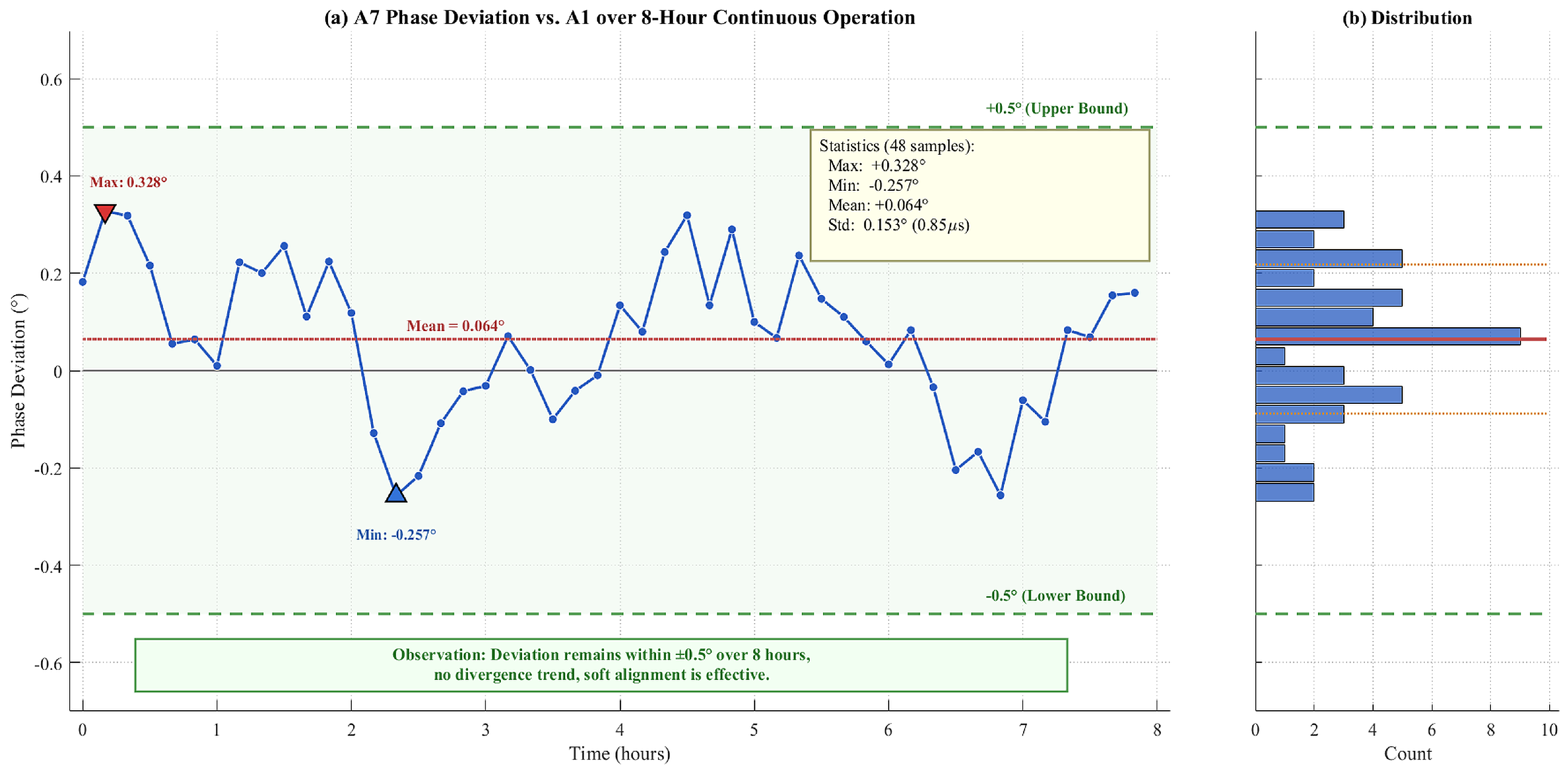
SourceTypeBasisBudgetMeasured EvidenceStatus
FPGA launchRandomCommon-trigger skew<100 nsNot isolatedTotal only
Fiber pathSystematic20 m × 5 ns/m100 nsLength envelopeGeometry-derived
Optical moduleSystematicDatasheet spread<500 nsNot isolatedAllocation
74HC14 + PCBSystematicCombined input path<200 nsNot de-embeddedCounted once
TIM3 quantizationQuantization1/17.5 MHz57 nsCCR stepDeterministic
Capture jitterRandomFilter/capture<100 nsNot isolatedTotal only
Dead bandAlgorithmicConfigured1000 nsFirmware settingBound
Oscillator residualSystematicAfter correction<500 nsδrel not loggedNo ±30 ppm guarantee
Worst-case totalGuaranteedLinear sum<2.56 μs (0.46°)Maximum 2.00 μsAggregate only
RSS totalEstimateIndependent terms<1.28 μs (0.23°)RMS 1.22 μs; 8 h SD 0.85 μsScale only
Table 13. Evidence-controlled comparison of the EXTI and TIM3 acquisition paths.
MetricEXTI Path on the Same PrototypeTIM3 Input-Capture PathEvidence Classification
Timestamp mechanismSoftware counter read after interruptHardware CCR1 latchImplementation fact
RMS phase/time errorNot measured0.22°/1.22 μsTIM3 measured; EXTI unavailable
Maximum phase/time errorNot measured0.36°/2.00 μs (inter-cell); +0.328°/+1.82 μs coarse-record maximumTIM3 measured at stated sampling
Short-term jitter/peak-to-peakNot available in the archived EXTI dataNot measured with cycle-resolved acquisitionUnavailable for both paths
Worst-case analytical bound>1.08°/>6 μs<0.46°/<2.56 μsAnalytical allocation
Synchronization establishmentNot reimplementedHard alignment within one 2 ms reference cycle; measured end-to-end recovery < 2 sImplementation plus TIM3 recovery measurement
CPU utilizationNot instrumentedNot instrumented; timestamp itself is peripheral-latchedNo quantitative utilization claim
Eight-hour stabilityNot measured0.153°/0.85 μs SD at 600 s samplingTIM3 coarse drift record only
Table 14. Comparison with conventional synchronization methods.
MethodSynchronization AccuracyNumber of Fiber OpticsUnit SwapHardware CostsSetup Speed
Centralized PWMSame Clock Domain144 Drive LinesNot supportedExtremely HighInstant
Dedicated sync lineNanosecond level72Requires bindingHighFast
Frame-header EXTI2–10 μs (estimated latency)36SupportedLowFast
Proposed TIM3 method1.22 μs RMS measured; <2.56 μs bound36SupportedLowFast
Purely distributed phase-locked loopDepends on convergence36SupportedLowSlow
Table 15. Prototype specifications.
ParametersValueUnit
Rated voltage13.8kV
Rated power3000kW
TopologyThree-phase CHB
Number of cells per phase12No.
Cell-rated voltage1100V
Carrier frequency500Hz
Carrier phase shift angle15°
ControllerDSP: TMS320F28335; FPGA: XC7A35T; cell controller: STM32F105RBT6 (36 controllers)
Communications36-channel downstream fiber, 2.5 Mbit/s
Table 16. Measured Phase-A cell offsets relative to A1.
Unit PairsTime Offset (μs)Phase Shift (°)Theoretical Value (°)Deviation (°)
A1-A28415.1215.00+0.12
A1-A316629.8830.00−0.12
A1-A425245.3645.00+0.36
A1-A533460.1260.00+0.12
A1-A641674.8875.00−0.12
A1-A750290.3690.00+0.36
A1-A8584105.12105.00+0.12
A1-A9666119.88120.00−0.12
A1-A10752135.36135.00+0.36
A1-A11832149.76150.00−0.24
A1-A12916164.88165.00−0.12
Table 17. Amplitude of the main frequency component.
FrequencyAmplitude (Relative to Fundamental)Notes
50 Hz0 dBFundamental frequency, modulation frequency
500 Hz−45 dBCell-carrier sideband, suppressed
1 kHz−42 dBSecond carrier group, suppressed
12 kHz−28 dBMain ripple, equivalent switching frequency
24 kHz−35 dBEquivalent switching frequency (2nd harmonic)
Table 18. Statistics on long-term stability over 8 h.
Statistical MeasuresPhase Deviation (°)Time Error (μs)
Maximum+0.328+1.82
Minimum−0.257−1.43
Mean+0.064+0.36
Standard deviation0.1530.85
Table 19. Comparison of the proposed method with representative state-of-the-art synchronization approaches.
MethodAccuracy and EvidenceFibers and Hardware (36 Cells)Establishment Time and ComputationScalability and Principal Limitation
Independent SYNC fiber [18]Nanosecond level; literature72 fibers; two receivers per cellOne pulse; negligible per-cell computationO (N) links with doubled transceivers; poor cabinet density
PTP/Ether CAT hardware timestamping [19,20,21,22]Sub-microsecond; literature36 bidirectional links; timestamp-capable interface and clock servoMultiple exchanges/servo updates; medium-high burdenNetwork-scalable but needs addressing, bidirectionality, and delay calibration
Frame-header EXTI [23]Microsecond level; load-dependent literature; 2–10 μs estimated here36 downstream fibers; GPIO interruptWithin one frame; low arithmetic but nondeterministic interrupt pathO (N) links; timing degrades with interrupt load
Protocol synchronization symbol [24]1–5 μs; literature36 downstream fibers; decoder supportAfter symbol decode; low-medium burden and bandwidth costO (N) links; recognition latency remains
Distributed locking/estimation [25,26,27]Method-dependent; literatureApplication-dependent feedback/current sensingIterative estimation; seconds or multiple cyclesNo dedicated SYNC link, but tuning, observability, and convergence limit scale
Proposed input-capture multiplexing0.22°/1.22 μs spatial RMS; 0.36°/2.00 μs maximum; measured for 12 active cells/phase36 existing downstream fibers; three pin ties; no added receiverHard alignment within one 2 ms cycle; O (1) capture, wrap, comparison, and ±1-count updatePer-cell O (1), master fan-out O (N); active-count scalability not experimentally swept
Disclaimer/Publisher’s Note: The statements, opinions and data contained in all publications are solely those of the individual author(s) and contributor(s) and not of MDPI and/or the editor(s). MDPI and/or the editor(s) disclaim responsibility for any injury to people or property resulting from any ideas, methods, instructions or products referred to in the content.