Three-Bridge LLC-LC Resonant Converter with Wide Output Voltage Control Ranges

 and
and
Abstract
1. Introduction
2. Proposed Three-Bridge LLC-LC Resonant Converter
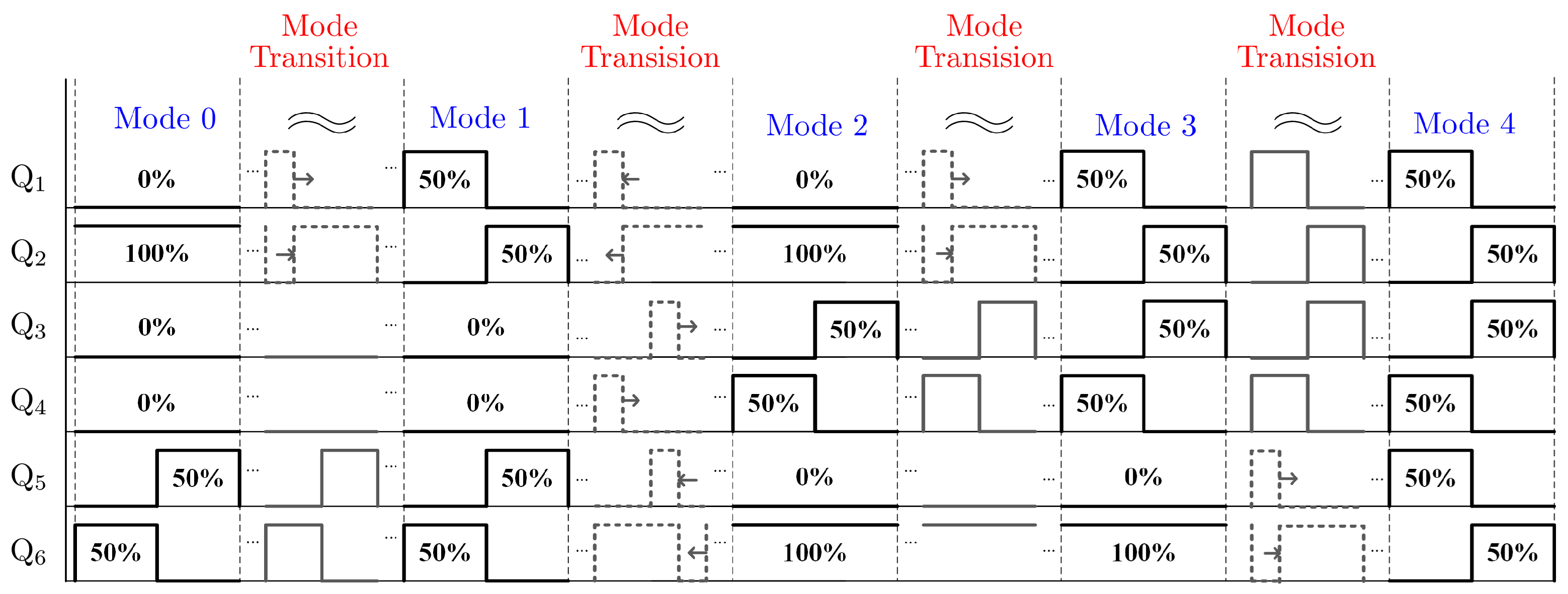
2.1. Circuit Topology and Operation Principles
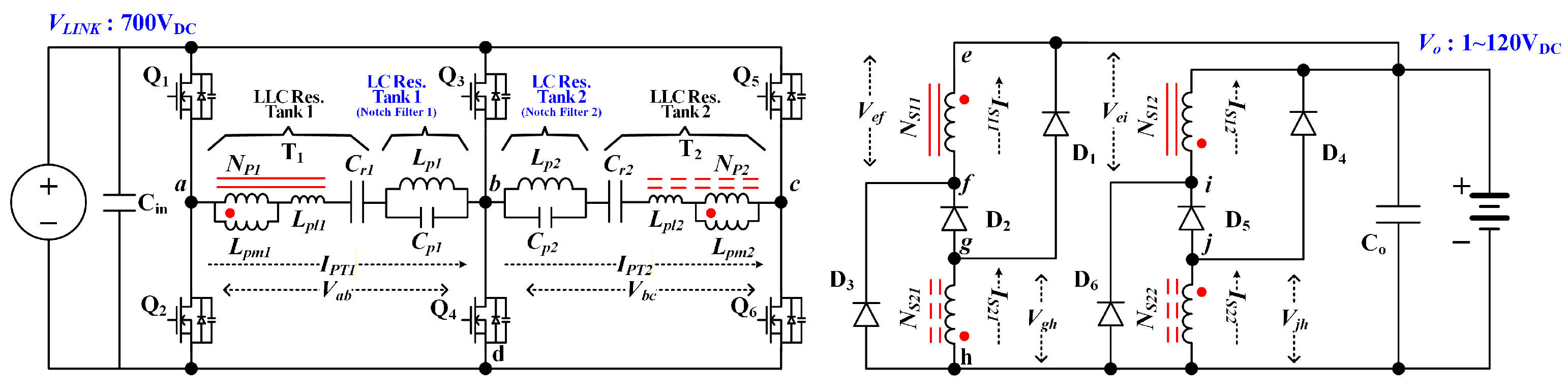
- LLC Res. Tank 1 and LLC Res. Tank 2 have the same parameters. , , , , .
- Notch filter 1 and notch filter 2 of parallel LC resonant circuit have the same parameters. , .
- Both transformers have the same turn ratio. , , .
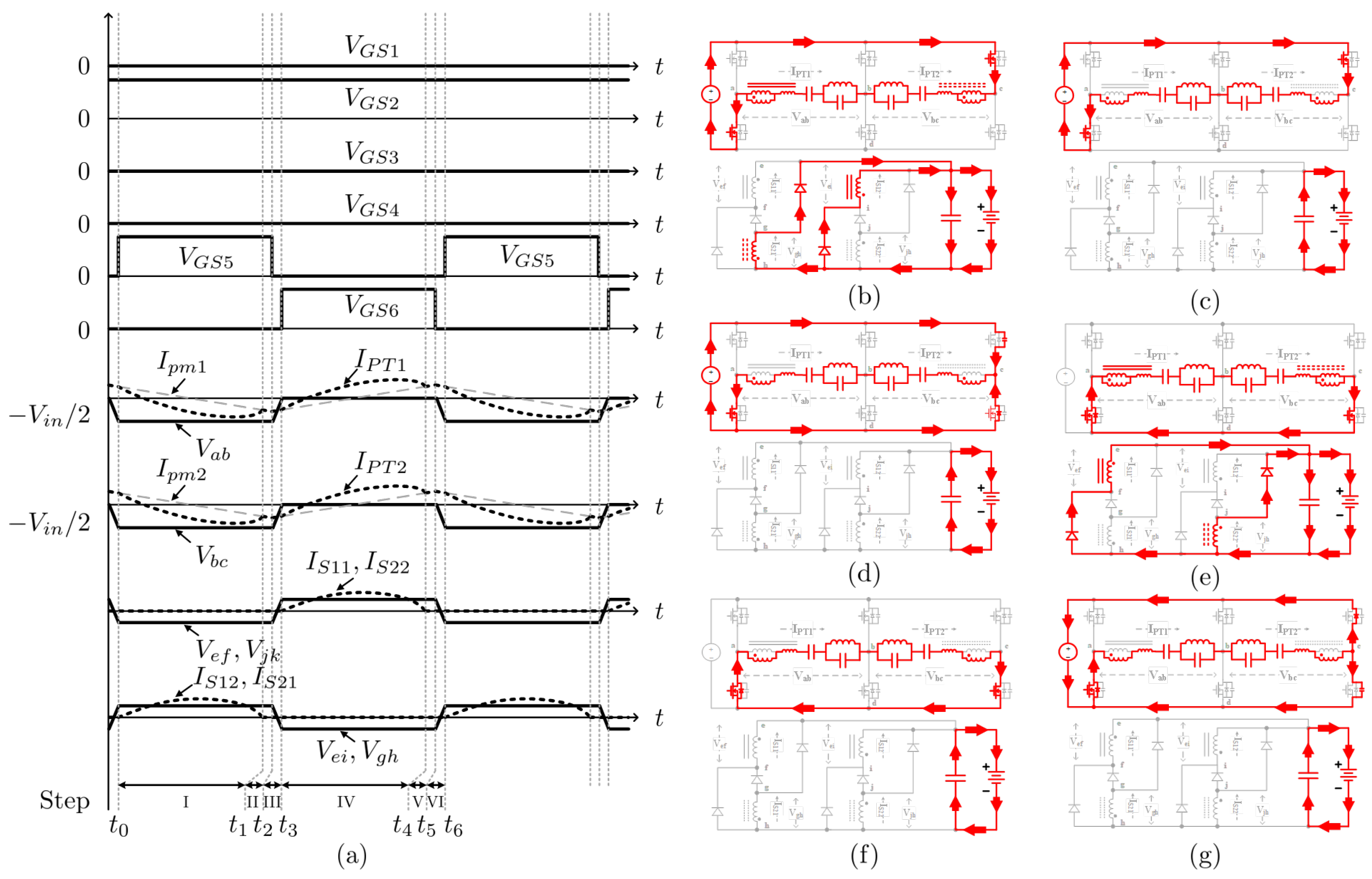
2.1.1. Steady-State Analysis in Mode 0
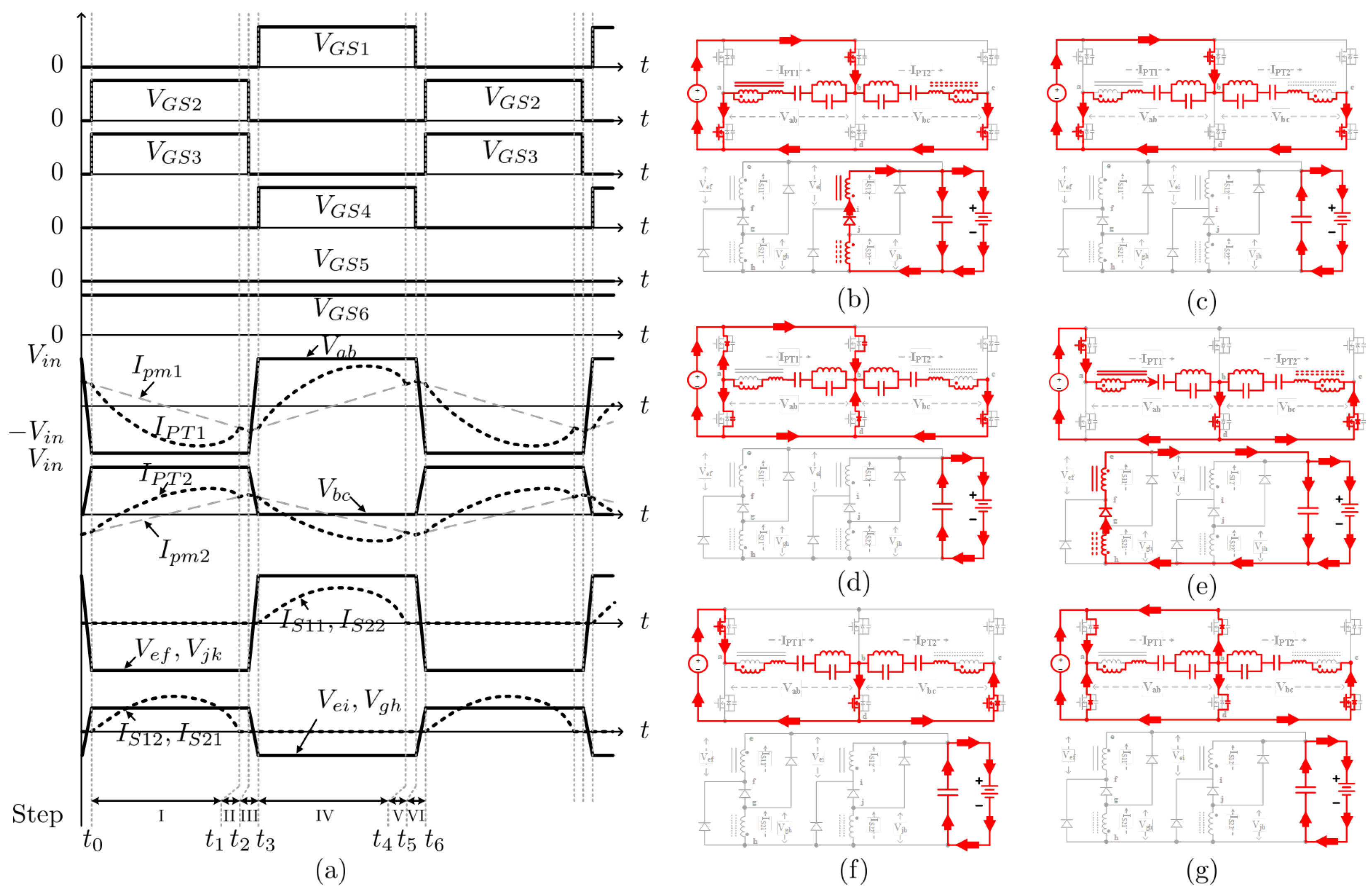
- Step 0-I (): In this step, the main switching device Q5 is turned on while Q6 is turned off. When the primary-side resonant current () flows through Q2 and Q5, the current decreases from positive to negative direction, causing the secondary-side rectifying diodes D1 and D6 to conduct. At this time, the voltage induced from the primary side is applied to the secondary side of the transformer. This step ends when the primary-side resonant current () becomes equal to the primary-side magnetizing current () and the transformer secondary-side current () becomes 0 A.
- Step 0-II (): and decrease to 0 A, causing D1 and D6 to become reverse-biased. At this time, the output load and the transformer secondary side operate separately, and and flow through and , the notch filter, and , causing to participate in resonance.
- Step 0-III (): When Q5 turns off at , the primary-side resonant voltage (, ) increases from –/2 to 0 , and and start to rise from negative to positive direction. Moreover, the parasitic capacitance-voltage of Q5 is charged to the input voltage, and simultaneously, the parasitic capacitance-voltage of Q6 is discharged to 0 .
- Step 0-IV–Step 0-VI (): The main switching device Q6 is turned on with ZVS when the primary-side resonant current (, ) is flowing through the anti-parallel diode of Q6 at . The input voltage is separated from the primary-side resonant circuit, and due to the energy stored in the resonant capacitor , and flow through Q2 and Q6, causing the secondary-side rectifying diodes D3 and D4 to conduct. For the remaining half-cycle, the subsequent operation is similar to step 0-I to step 0-III.
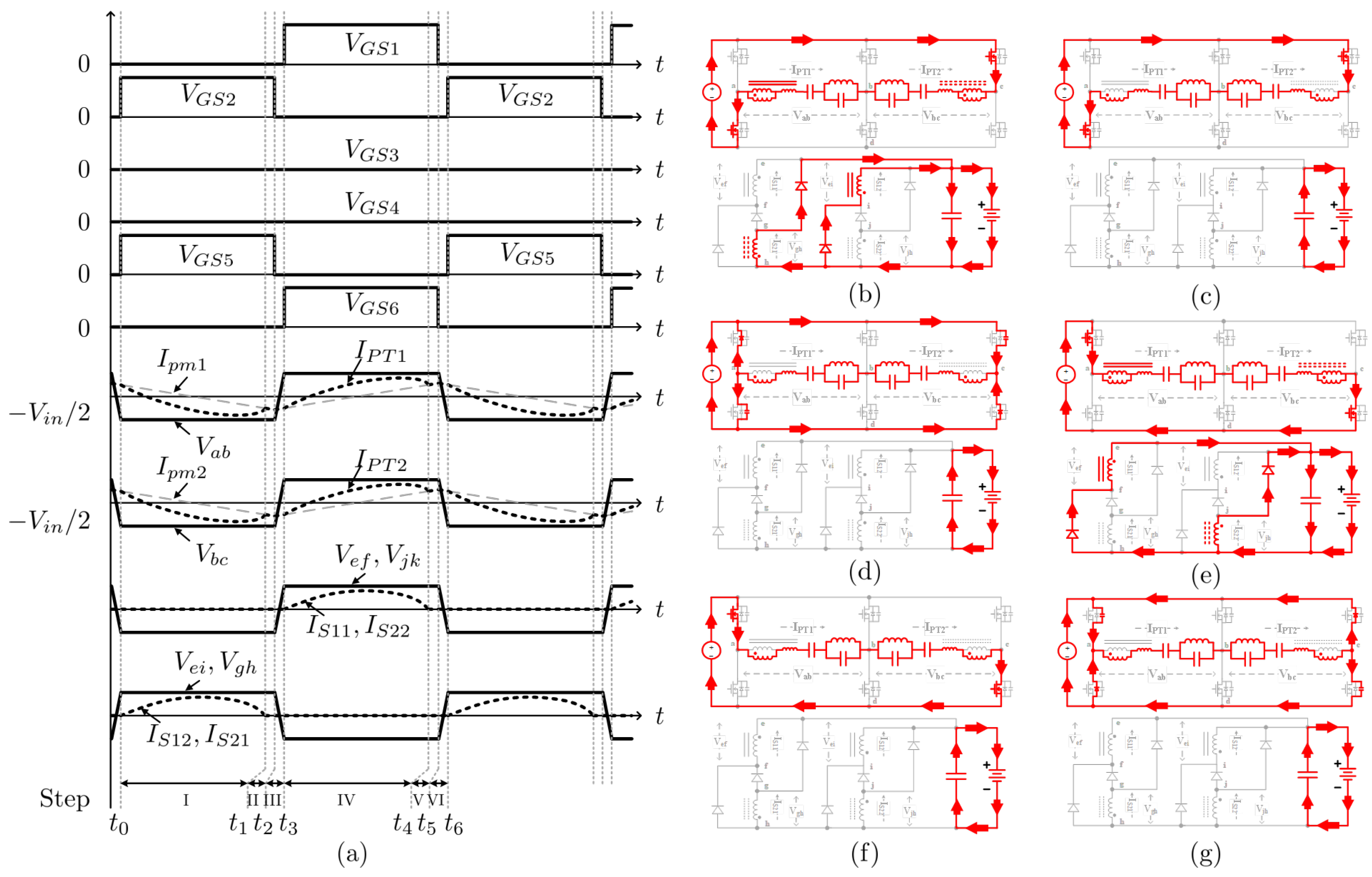
2.1.2. Steady-State Analysis in Mode 1
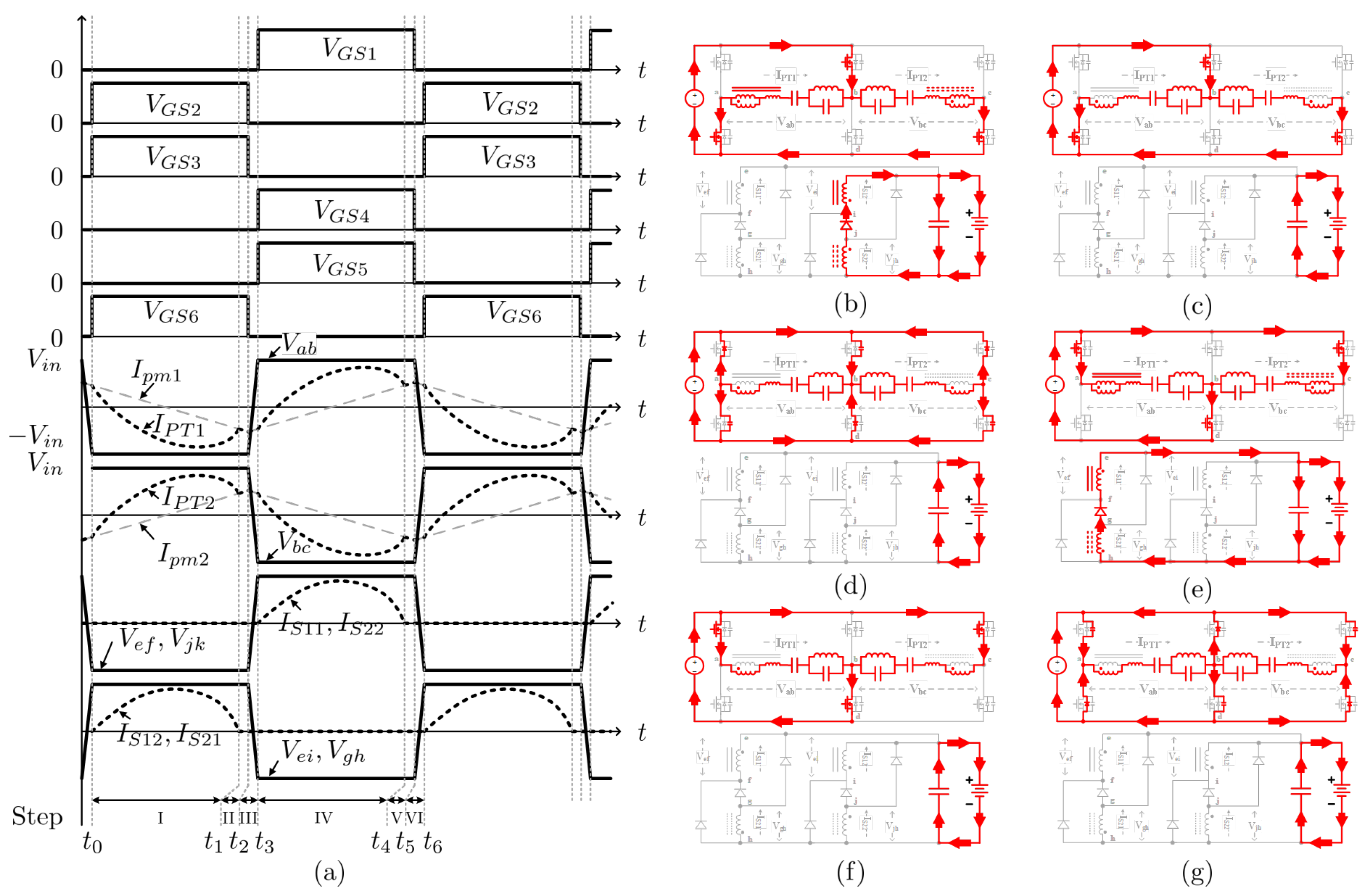
- Step 1-I–Step 1-II (): This interval operates the same as step 0-I to step 0-II explained earlier.
- Step 1-III (): When Q5 turns off at , and increase from –/2 to /2, and and start to rise from negative to positive direction. Moreover, the parasitic capacitors of Q2 and Q5 are charged to the input voltage (), and simultaneously, the parasitic capacitors of Q1 and Q6 are discharged to 0 .
- Step 1-IV (): The main switching devices Q1 and Q6 at are turned on with ZVS when the primary-side resonant current (, ) is flowing through the anti-parallel diodes of Q1 and Q6. Furthermore, and start flowing through Q1 and Q6, with the current rising in the positive direction. At this time, D3 and D4 conduct, and the voltage induced from the primary side is applied to the secondary side of the transformer. This step ends when and become equal to and , and the transformer secondary-side currents (, ) become 0 A.
- Step 1-V (): and decrease to 0 A, causing D3 and D4 to become reverse-biased. At this time, the output load and the transformer secondary side operate separately, and and flow through and , the notch filter, and , causing to participate in resonance.
- Step 1-VI (): When Q1 and Q6 turn off at , and decrease from /2 to –/2, and and start to fall from positive to negative direction. Moreover, the parasitic capacitors of Q1 and Q6 are charged to the input voltage (), and simultaneously, the parasitic capacitors of Q2 and Q5 are discharged to 0 .
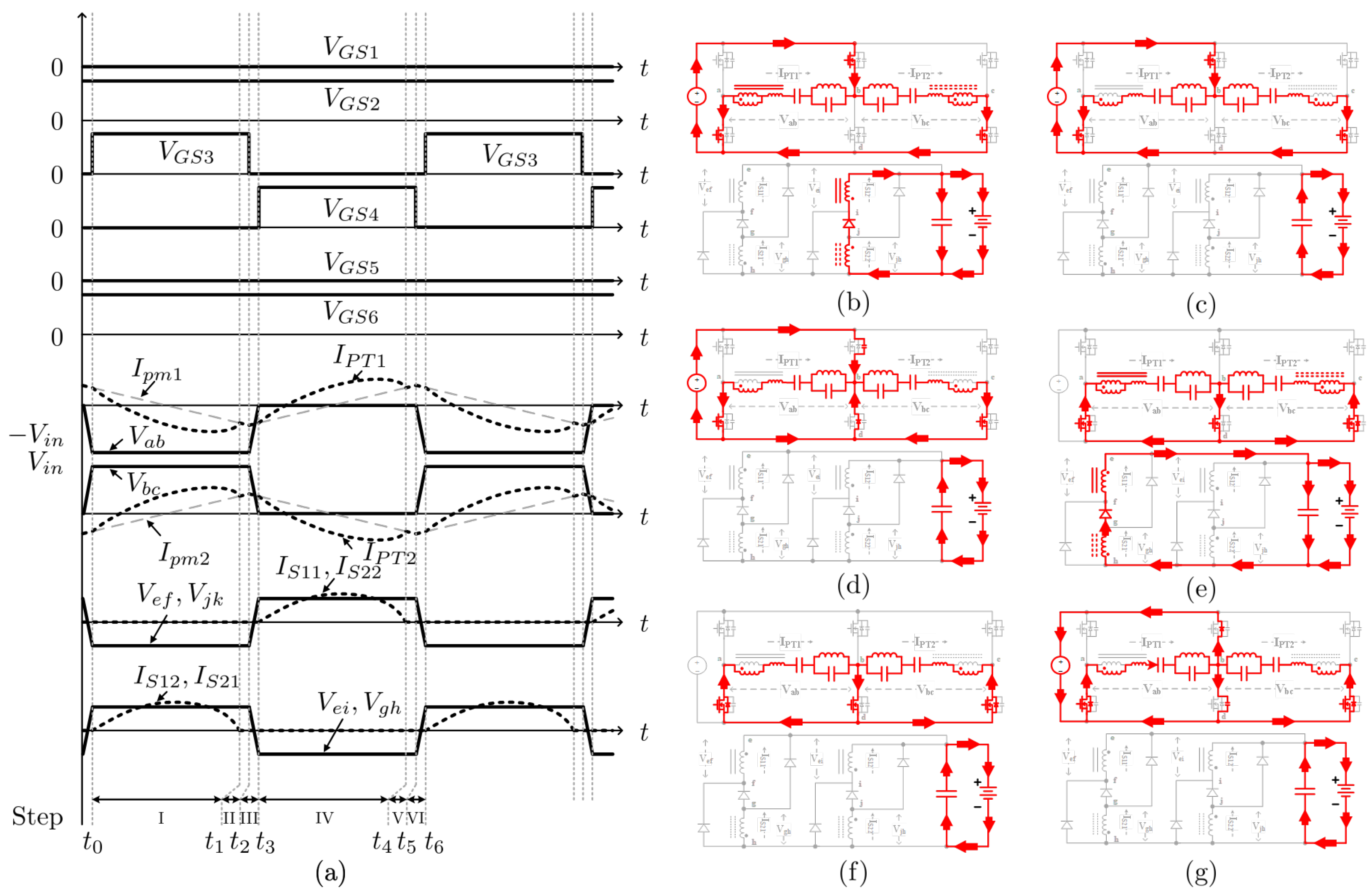
2.1.3. Steady-State Analysis in Mode 2
- Step 2-I (): In this step, the main switching device Q3 is turned on while Q4 is turned off from the previous step. When the primary-side resonant current flows through Q3, Q2, and Q6, decreases from positive to negative direction, and rises in the opposite direction, causing the secondary-side rectifying diode D5 to conduct. At this time, the voltage induced from the primary side is applied to the secondary side of the transformer, and the magnetic energy of increases linearly, with not participating in resonance. This step ends when and become equal to and , and and become 0 A.
- Step 2-II (): and decrease to 0 A, causing D5 to become reverse-biased. Currently, the output load and the transformer secondary side operate separately, and and flow through the notch filter, , , and , causing to participate in resonance.
- Step 2-III (): When Q3 turns off at , increases from – to 0 , and decreases from to 0 . At this time, and start to rise and fall in the opposite direction of their previous flow. Moreover, the parasitic capacitor of Q3 is charged to the input voltage (), and simultaneously, the parasitic capacitor of Q4 is discharged to 0 .
- Step 2-IV–Step 2-VI (): For the remaining half-cycle, Q4 is turned on while Q3 is turned off from the previous step. The input voltage is separated from the primary-side resonant circuit, and due to the energy stored in the resonant capacitor , the primary-side resonant current flows through Q4, Q2, and Q6, causing the secondary-side rectifying diode D2 to conduct. The subsequent operation is similar to step 2-I to step 2-III.
2.1.4. Steady-State Analysis in Mode 3
- Step 3-I–Step 3-II (): This interval operates the same as step 2-I to step 2-II explained earlier.
- Step 3-III (): and become 0 , and Q2 and Q3 turn off. As a result, increases from – to , and decreases from to 0 . At this time, and rise and fall in the opposite direction of their previous flow. Moreover, the parasitic capacitors of Q2 and Q3 are charged to the input voltage (), and simultaneously, the parasitic capacitors of Q1 and Q4 are discharged to 0 .
- Step 3-IV (): Q1 and Q4 turn on with ZVS condition due to the resonant current flowing through anti-parallel diodes of Q1 and Q4, and flows through Q1 and Q4, with the current rising from negative to positive direction. In contrast, flows through Q4 and Q6, falling in the opposite direction. This causes D2 to conduct. At this time, voltage induced from resonant tank 1 and voltage induced from resonant tank 2 are applied to the secondary side of the transformer, and the magnetic energy of increases linearly, with not participating in resonance. This step ends when and become equal to and , and and become 0 A.
- Step 3-V (): and decrease to 0 A, causing D2 to become reverse-biased. Currently, the output load and the transformer secondary side operate separately, and and flow through , , , and the notch filter, causing to participate in resonance.
2.1.5. Steady-State Analysis in Mode 4
- Step 4-I–Step 4-II (): This interval operates the same as step 2-I to step 2-II explained earlier.
- Step 4-III (): At , , , and become 0 , and Q2, Q3, and Q6 turn off. As a result, increases from – to , and decreases from to –. At this time, and rise and fall in the opposite direction of their previous flow. Moreover, the parasitic capacitors of Q2, Q3, and Q6 are charged to the input voltage (), and simultaneously, the parasitic capacitors of Q1, Q4, and Q5 are discharged to 0 .
- Step 4-IV (): The main switching devices Q1, Q4, and Q5 turn on, and flows through Q1 and Q4, rising from negative to positive direction, while flows through Q5 and Q4, falling in the opposite direction. This causes D2 to conduct. At this time, the voltage induced from the primary side is applied to the secondary side of the transformer, and the magnetic energy of increases linearly, with not participating in resonance. This step ends when and become equal to and , and and become 0 A.
- Step 4-V (): and decrease to 0 A, causing D2 to become reverse-biased. Currently, the output load and the transformer secondary side operate separately, and and flow through , , , and the notch filter, causing to participate in resonance.
- Step 4-VI (): At , Q1, Q4, and Q5 turn off; as a result, decreases from to –, and increases from – to . and start to fall and rise in the opposite direction of their previous flow. Moreover, the parasitic capacitors of Q1, Q4, and Q5 are charged to the input voltage, and simultaneously, the parasitic capacitors of Q2, Q3, and Q6 are discharged to 0 .
2.2. Input Impedance Characteristics
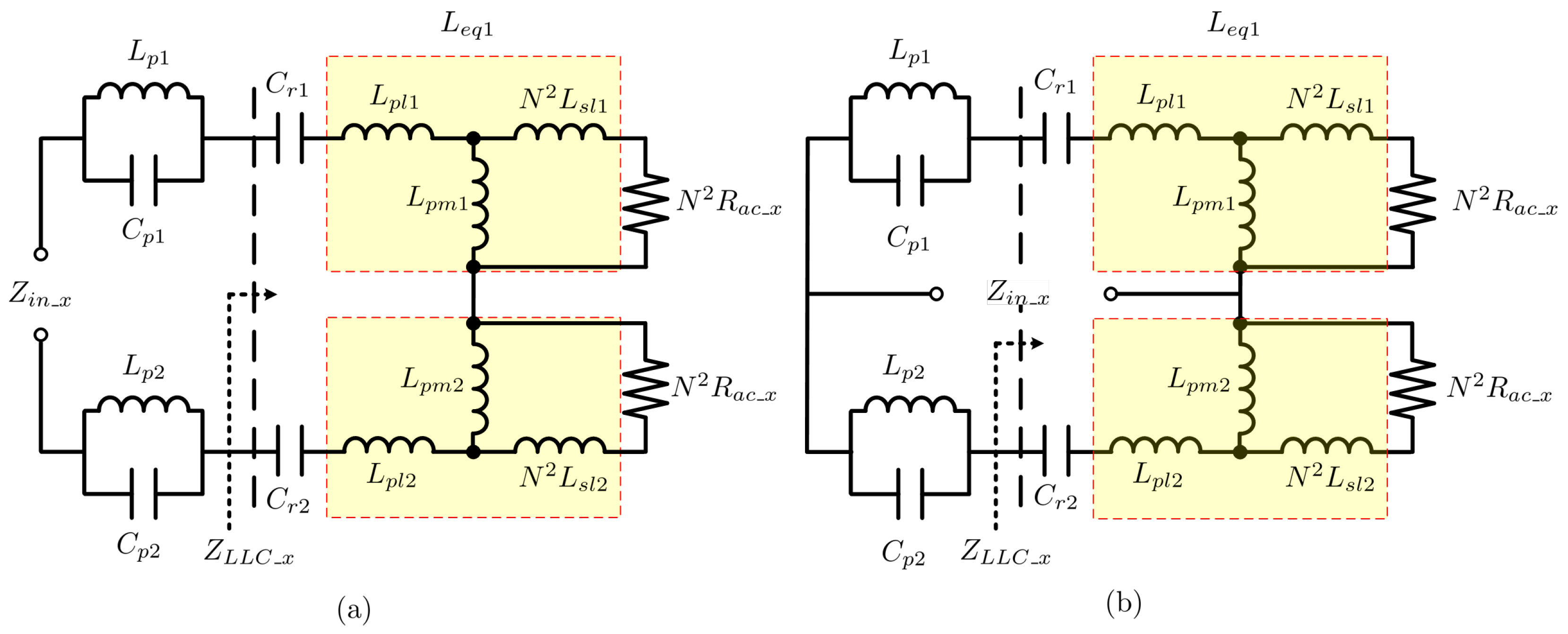
- , 1st leakage/magnetizing inductance ratio
- , 2nd leakage/magnetizing inductance ratio as seen from the 1st side
- , equivalent leakage inductance
- , LC parallel resonant load quality factor
- , LLC series resonant load quality factor
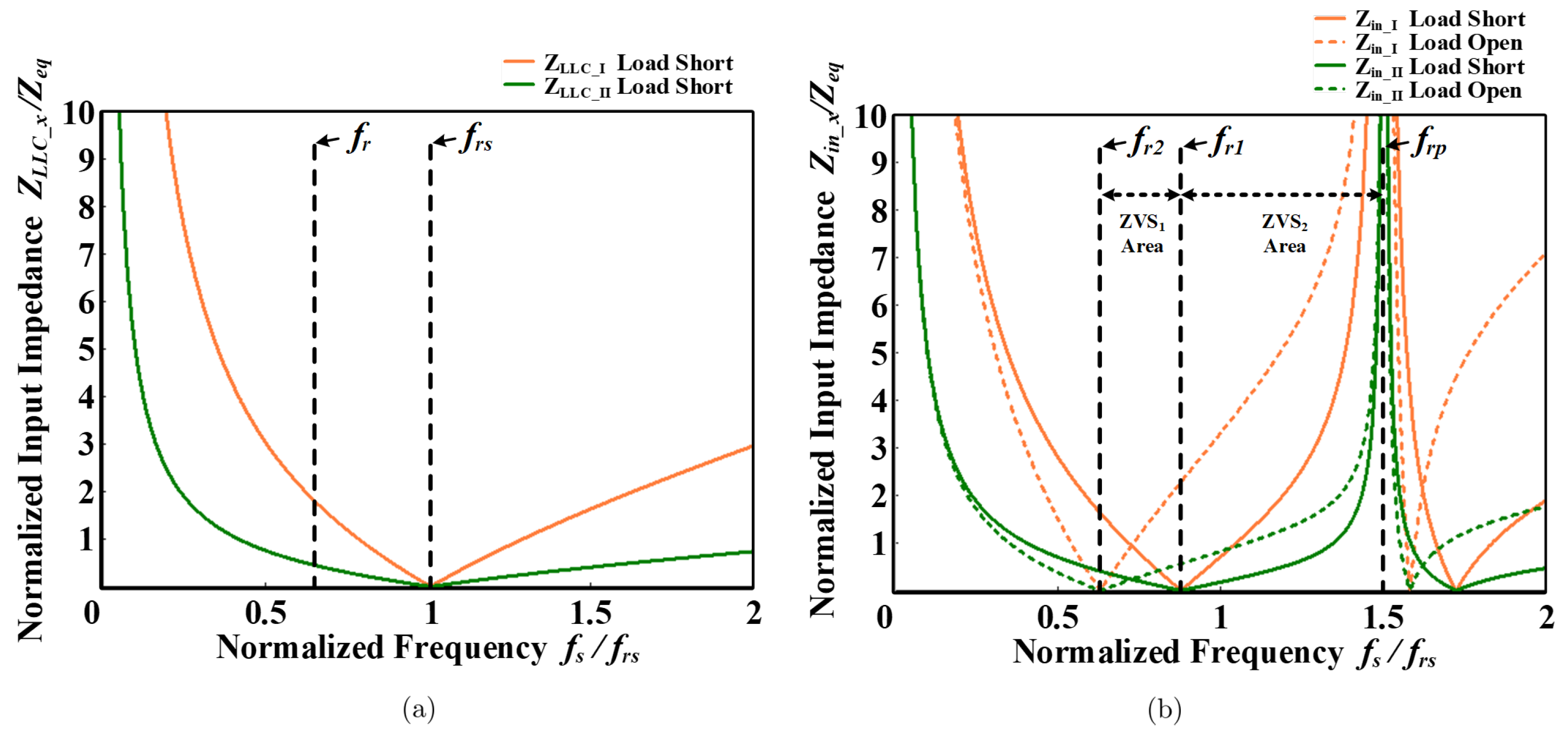
- , switching frequency normalized to LC parallel resonant frequency
- , switching frequency normalized to LLC series resonant frequency
- , LLC Series /LC parallel resonant characteristic impedance ratio
- , LLC series resonant characteristic impedance
- , LLC series resonant characteristic impedance
- , LLC resonant characteristic impedance
- , LC parallel resonant characteristic impedance
2.3. Input–Output Voltage Gain Characteristics
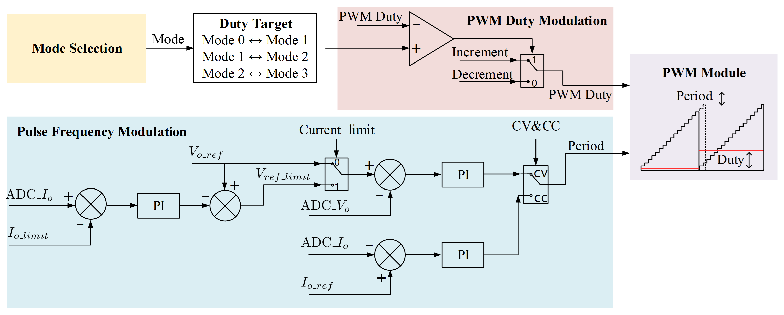
2.4. Control Algorithm for 3-Bridge LLC-LC Resonant Converter
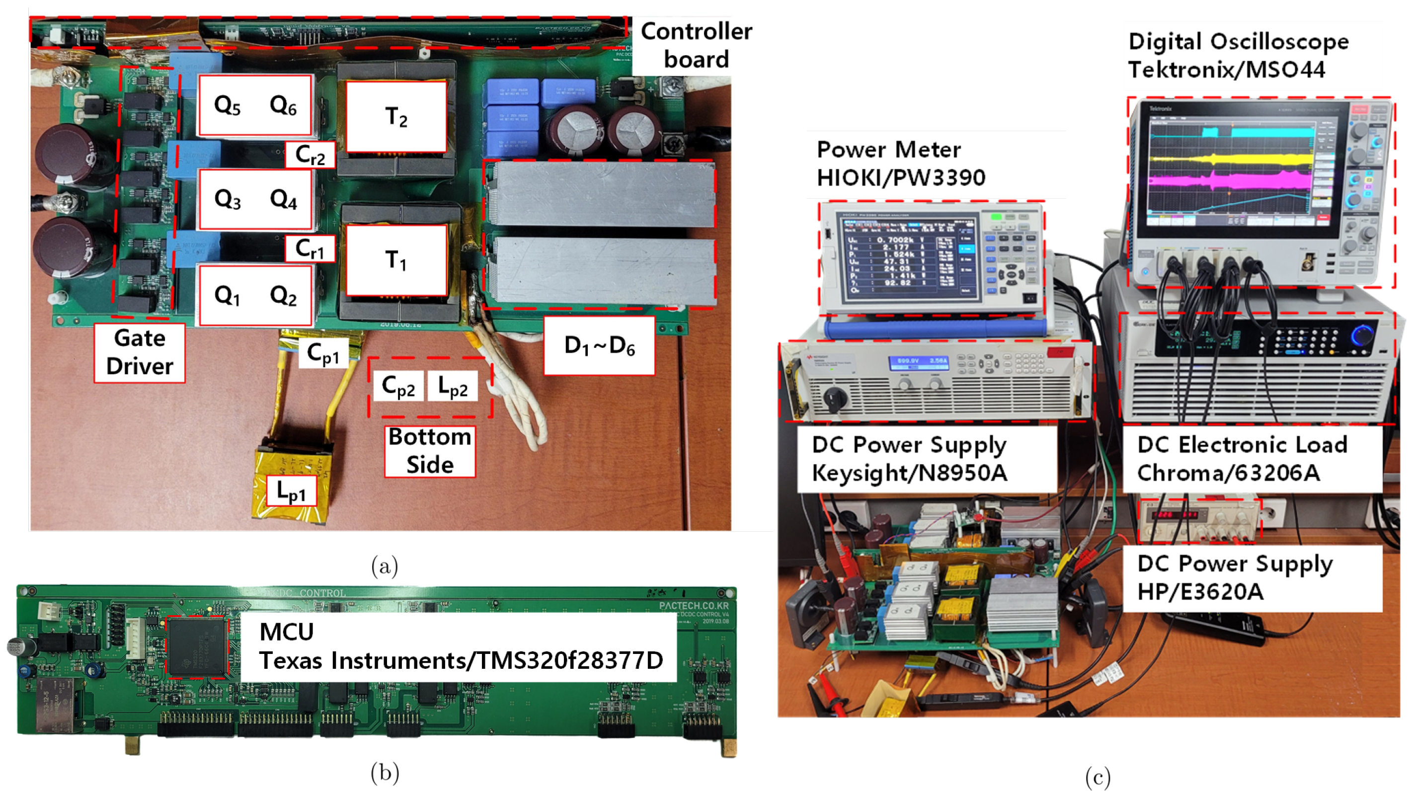
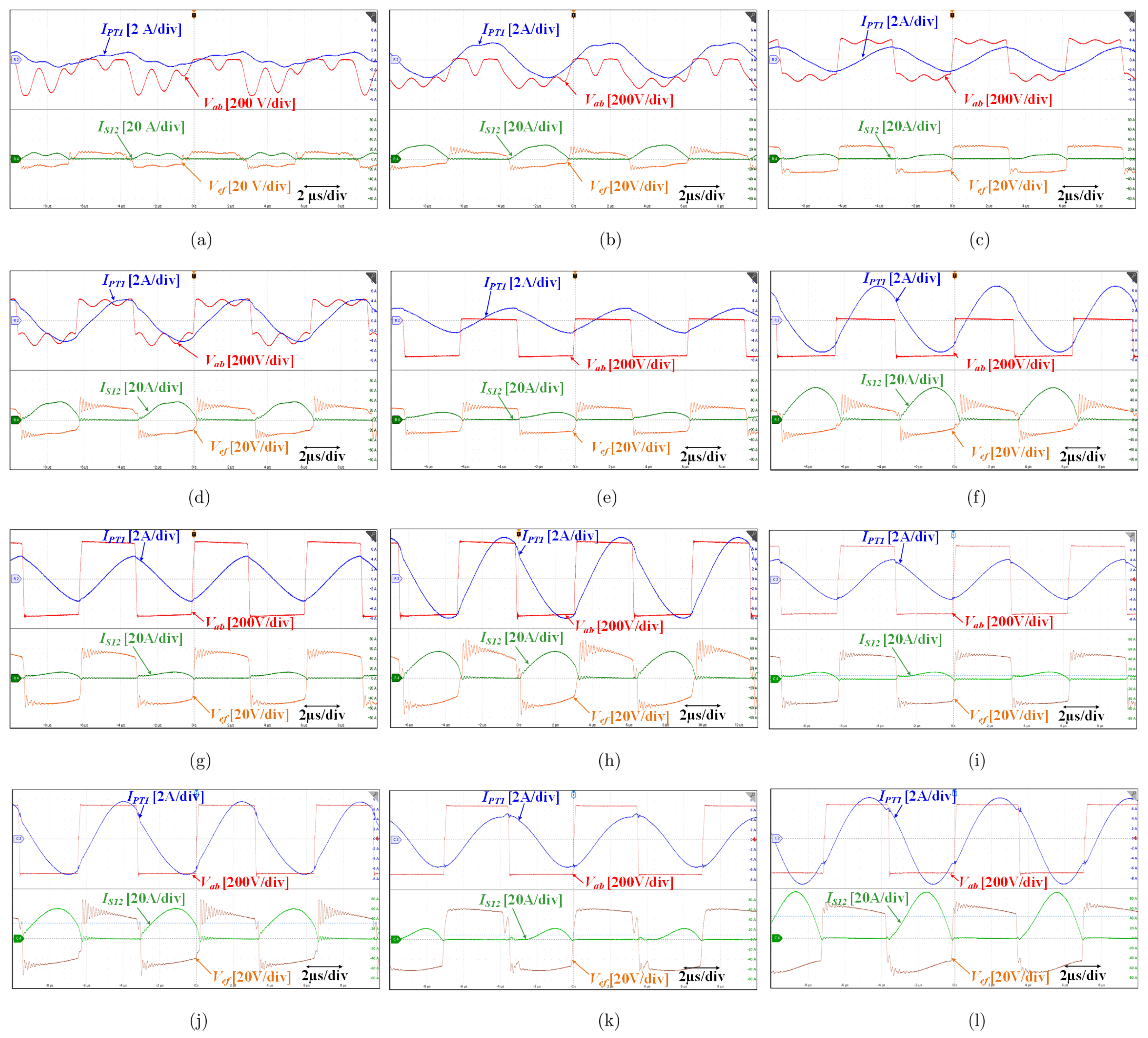
3. Experiment Results
4. Conclusions
Author Contributions
Funding
Institutional Review Board Statement
Informed Consent Statement
Data Availability Statement
Conflicts of Interest
References
- Deng, J.; Mi, C.C.; Ma, R.; Li, S. Design of LLC Resonant Converters Based on Operation-Mode Analysis for Level Two PHEV Battery Chargers. IEEE/ASME Trans. Mechatron. 2015, 20, 1595–1606. [Google Scholar] [CrossRef]
- Xu, H.; Yin, Z.; Zhao, Y.; Huang, Y. Accurate Design of High-Efficiency LLC Resonant Converter with Wide Output Voltage. IEEE Access 2017, 5, 26653–26665. [Google Scholar] [CrossRef]
- Ivensky, G.; Bronshtein, S.; Abramovitz, A. Approximate Analysis of Resonant LLC DC-DC Converter. IEEE Trans. Power Electron. 2011, 26, 3274–3284. [Google Scholar] [CrossRef]
- Beiranvand, R.; Rashidian, B.; Zolghadri, M.R.; Alavi, S.M.H. Using LLC Resonant Converter for Designing Wide-Range Voltage Source. IEEE Trans. Ind. Electron. 2011, 58, 1746–1756. [Google Scholar] [CrossRef]
- Li, B.; Li, Q.; Lee, F.C.; Liu, Z.; Yang, Y. A High-Efficiency High-Density Wide-Bandgap Device-Based Bidirectional On-Board Charger. IEEE J. Emerg. Sel. Top. Power Electron. 2018, 6, 1627–1636. [Google Scholar] [CrossRef]
- Lee, J.B.; Kim, J.K.; Baek, J.I.; Kim, J.H.; Moon, G.W. Resonant Capacitor On/Off Control of Half-Bridge LLC Converter for High-Efficiency Server Power Supply. IEEE Trans. Ind. Electron. 2016, 63, 5410–5415. [Google Scholar] [CrossRef]
- Jeong, Y.; Moon, G.W.; Kim, J.K. Analysis on half-bridge LLC resonant converter by using variable inductance for high efficiency and power density server power supply. In Proceedings of the 2017 IEEE Applied Power Electronics Conference and Exposition (APEC); IEEE: New York, NY, USA, 2017; pp. 170–177. [Google Scholar] [CrossRef]
- Li, C.; Zhou, M.; Wang, H. An H5-Bridge-Based Asymmetric LLC Resonant Converter with an Ultrawide Output Voltage Range. IEEE Trans. Ind. Electron. 2020, 67, 9503–9514. [Google Scholar] [CrossRef]
- Shu, D.; Wang, H. An Ultrawide Output Range LLC Resonant Converter Based on Adjustable Turns Ratio Transformer and Reconfigurable Bridge. IEEE Trans. Ind. Electron. 2021, 68, 7115–7124. [Google Scholar] [CrossRef]
- Park, M.H.; Jeong, Y.; Rorrer, R.A.L.; Choi, D.; Moon, G.W. Hold-Up Time Extension Method for LLC Resonant Converter by Detecting Operation Region. IEEE Trans. Power Electron. 2020, 35, 9949–9952. [Google Scholar] [CrossRef]
- Liang, Z.; Guo, R.; Wang, G.; Huang, A. A new wide input range high efficiency photovoltaic inverter. In Proceedings of the 2010 IEEE Energy Conversion Congress and Exposition; IEEE: New York, NY, USA, 2010; pp. 2937–2943. [Google Scholar] [CrossRef]
- Sun, W.; Xing, Y.; Wu, H.; Ding, J. Modified High-Efficiency LLC Converters with Two Split Resonant Branches for Wide Input-Voltage Range Applications. IEEE Trans. Power Electron. 2018, 33, 7867–7879. [Google Scholar] [CrossRef]
- Hu, H.; Fang, X.; Chen, F.; Shen, Z.J.; Batarseh, I. A Modified High-Efficiency LLC Converter with Two Transformers for Wide Input-Voltage Range Applications. IEEE Trans. Power Electron. 2013, 28, 1946–1960. [Google Scholar] [CrossRef]
- Li, C.; Wang, H.; Shang, M. A Five-Switch Bridge Based Reconfigurable LLC Converter for Deeply Depleted PEV Charging Applications. IEEE Trans. Power Electron. 2019, 34, 4031–4035. [Google Scholar] [CrossRef]
- Hu, H.; Fang, X.; Zhang, Q.; Shen, Z.J.; Batarseh, I. Optimal Design Considerations for a Modified LLC converter with wide input voltage range capability suitable for PV applications. In Proceedings of the 2011 IEEE Energy Conversion Congress and Exposition; IEEE: New York, NY, USA, 2011; pp. 3096–3103. [Google Scholar] [CrossRef]
- Jovanović, M.M.; Irving, B.T. On-the-Fly Topology-Morphing Control—Efficiency Optimization Method for LLC Resonant Converters Operating in Wide Input- and/or Output-Voltage Range. IEEE Trans. Power Electron. 2016, 31, 2596–2608. [Google Scholar] [CrossRef]
- Wei, Y.; Luo, Q.; Alan Mantooth, H. A Novel LLC Converter with Topology Morphing Control for Wide Input Voltage Range Application. IEEE J. Emerg. Sel. Top. Power Electron. 2022, 10, 1563–1574. [Google Scholar] [CrossRef]
- Mudiyanselage, G.A.; Kozielski, K.; Emadi, A. Optimal LLC Converter Design with Topology Morphing Control for Wide Voltage Range Battery Charging Applications. IEEE Open J. Power Electron. 2024, 5, 1209–1226. [Google Scholar] [CrossRef]
- Wu, H.; Zhan, X.; Xing, Y. Interleaved LLC Resonant Converter with Hybrid Rectifier and Variable-Frequency Plus Phase-Shift Control for Wide Output Voltage Range Applications. IEEE Trans. Power Electron. 2017, 32, 4246–4257. [Google Scholar] [CrossRef]
- Yoo, S.; Kim, M.; Kim, E. 3-Bridge LLC resonant converter for achieving wide output voltage control range based on topology morphing. J. Power Electron. 2020, 20, 1420–1432. [Google Scholar] [CrossRef]
- Park, K.S.; Kim, T.R.; Kim, E.S.; Jeon, Y.S. 3-Bridge LLC DC-DC Converter with Notch Filter for Wide Output Voltage Control. In Proceedings of the 2024 IEEE 10th International Power Electronics and Motion Control Conference (IPEMC2024-ECCE Asia); IEEE: New York, NY, USA, 2024; pp. 4959–4964. [Google Scholar] [CrossRef]
- Kim, J.W.; Kang, M.G.; Gong, S.U.; Park, J.S.; Park, J.H.; Won, J.S.; Kim, E.S. Three-Bridge LLC Resonant Converter with 5 Operation Mode Transitions for Wide Output Voltage Control. Energies 2026, 19, 590. [Google Scholar] [CrossRef]
- Yang, B.; Lee, F.; Concannon, M. Over current protection methods for LLC resonant converter. In Proceedings of the Eighteenth Annual IEEE Applied Power Electronics Conference and Exposition (APEC ’03); IEEE: New York, NY, USA, 2003; Volume 2, pp. 605–609. [Google Scholar] [CrossRef]
- Han, F.; Wang, Y.; Yang, L.; Chen, M.; Liu, R.; Xu, R. High-efficiency topology-morphing multi-resonant DC–DC converter with wide voltage gain range for small-scale wind generation applications. IET Power Electron. 2019, 12, 2330–2337. [Google Scholar] [CrossRef]
- Mishima, T.; Mizutani, H.; Nakaoka, M. A Sensitivity-Improved PFM LLC Resonant Full-Bridge DC–DC Converter with LC Antiresonant Circuitry. IEEE Trans. Power Electron. 2017, 32, 310–324. [Google Scholar] [CrossRef]
- Chen, M.; Chen, B.; Wang, P.; Wang, Y.; Zhang, M. A High Efficiency and Wide Voltage Gain sLC_LCC DC–DC Converter with SiC Devices. IEEE Trans. Power Electron. 2023, 38, 2169–2180. [Google Scholar] [CrossRef]
- Zhao, Q.; Liu, W.; Wang, Y.; Wang, D.; Wu, N. A Novel Multiresonant DC–DC Converter with Wide Output-Voltage Range. IEEE Trans. Power Electron. 2020, 35, 5625–5638. [Google Scholar] [CrossRef]
- Wu, H.; Jin, X.; Hu, H.; Xing, Y. Multielement Resonant Converters with a Notch Filter on Secondary Side. IEEE Trans. Power Electron. 2016, 31, 3999–4004. [Google Scholar] [CrossRef]



| Parameters | Value |
|---|---|
| Input voltage, | 700 |
| Output voltage range, | 1 –120 |
| Output current range, | 5–50 A |
| Output power range, | 6 kW |
| 1st LLC-LC resonant frequency, | 148 kHz |
| 2nd LLC-LC resonant frequency, | 101 kHz |
| LC parallel resonant frequency, | 255 kHz |
| Switching frequency range, | 140–255 kHz |
| Switching devices, Q1–Q6 | UJ3C120040K3S (1200 , 65 A, 35 mΩ, SiC) |
| Output diodes, D1, D3, D4, D6/D2, D5 | UJ3D06560KS/UJ3D06560KS × 2 (650 , 60 A, VF: 1.5 , SiC) |
| Parameters | Value |
|---|---|
| Transformer turn ratio, | 18 (=36/2) |
| Primary leakage inductance, / | 28.20 μH/28.09 μH |
| Secondary leakage inductance, / | 541.00 nH/545.00 nH |
| Magnetizing inductance, / | 291.13 μH/288.48 μH |
| Equivalent leakage inductance, / | 137.67 μH/137.58 μH |
| LLC resonant capacitor, / | 6.30 nF/6.33 nF |
| LC parallel resonant inductance, / | 28.79 μH/28.66 μH |
| LC parallel resonant capacitor, / | 13.52 nF/13.43 nF |
Disclaimer/Publisher’s Note: The statements, opinions and data contained in all publications are solely those of the individual author(s) and contributor(s) and not of MDPI and/or the editor(s). MDPI and/or the editor(s) disclaim responsibility for any injury to people or property resulting from any ideas, methods, instructions or products referred to in the content. |
© 2026 by the authors. Licensee MDPI, Basel, Switzerland. This article is an open access article distributed under the terms and conditions of the Creative Commons Attribution (CC BY) license.
Share and Cite
Kim, T.; Kim, J.-w.; Park, J.-h.; Choi, J.; Won, J.-S.; Kim, E.-s. Three-Bridge LLC-LC Resonant Converter with Wide Output Voltage Control Ranges. Energies 2026, 19, 3523. https://doi.org/10.3390/en19153523
Kim T, Kim J-w, Park J-h, Choi J, Won J-S, Kim E-s. Three-Bridge LLC-LC Resonant Converter with Wide Output Voltage Control Ranges. Energies. 2026; 19(15):3523. https://doi.org/10.3390/en19153523
Chicago/Turabian StyleKim, Taeran, Jin-woo Kim, Jun-hyoung Park, Joonyoung Choi, Jong-Seob Won, and Eun-soo Kim. 2026. "Three-Bridge LLC-LC Resonant Converter with Wide Output Voltage Control Ranges" Energies 19, no. 15: 3523. https://doi.org/10.3390/en19153523
APA StyleKim, T., Kim, J.-w., Park, J.-h., Choi, J., Won, J.-S., & Kim, E.-s. (2026). Three-Bridge LLC-LC Resonant Converter with Wide Output Voltage Control Ranges. Energies, 19(15), 3523. https://doi.org/10.3390/en19153523