1. Introduction
Compared to conventional plug-in power systems, Wireless Power Transfer (WPT) technology exhibits superior advantages, including enhanced reliability, advanced intelligence, and exceptional flexibility [
1]. To date, WPT technology has been extensively deployed across diverse fields, such as electric vehicles [
2], biomedical devices [
3], intelligent inspection robots [
4], and smart wearable electronics [
5].
Efficient power conversion is critical in self-powered and energy-harvesting systems, where available energy is limited and dynamic load conditions are highly variable. Recent review works provide comprehensive overviews of energy harvesting technologies and the associated converter design challenges, highlighting the importance of high efficiency and robust dynamic performance in practical applications, including autonomous sensors, wearable electronics, and wireless power transfer systems [
6,
7,
8]. These studies further motivate the development of converter topologies capable of achieving both high efficiency and fast dynamic response.
In WPT systems, a Buck converter is commonly cascaded with the receiver-side rectifier to tightly regulate the output voltage. Conventional studies suggest that the control-to-output transfer function of a standard Buck converter lacks a right-half-plane zero (RHPz), characterizing it as a minimum-phase system with excellent controllability [
9]. However, this paradigm shifts in WPT scenarios. Integrating constant-current (CC) output compensation networks, including S–S, LCC–LCC, and LCL–LCL configurations [
10], forces the Buck converter’s input capacitor to inherently give rise to an RHPz within the transfer function. Consequently, the control system degrades into a non-minimum-phase system [
11].
In the time domain, an RHPz manifests as an inverse response to a step change, where the deviation between the actual and reference values of the controlled variable initially widens before narrowing [
12]. During this inverse response phase, the controller perceives misleading feedback signals, which prolongs the settling time, degrades system stability, and may even trigger positive feedback, ultimately leading to output instability [
13]. Furthermore, the achievable control bandwidth of non-minimum-phase systems is typically constrained by the RHPz. Consequently, mitigating the adverse effects of the RHPz is of paramount importance for enhancing both the stability and dynamic performance of the system.
Recent studies suggest that the dynamic performance of WPT systems can be enhanced through optimized parameter design [
14]. By analyzing the influence of input capacitance on voltage ripple and the location of the RHPz, a calculation method for the critical input capacitance has been proposed. While this strategy partially mitigates the adverse effects of the RHPz, it fails to fundamentally eliminate them. Building upon this, Reference [
15] further reveals that an exceptionally small input capacitance forces the Buck converter into a discontinuous input voltage operation mode. Although this mode successfully removes the RHPz from the transfer function, the excessively small capacitance inevitably induces severe input voltage ripples.
To address issues associated with the RHPz, various advanced control strategies have been proposed. Reference [
16] introduced a dual-loop control method that incorporates an inner input-voltage loop into the original outer output-voltage control scheme, thereby accelerating the system’s response speed. Reference [
17] employed an input-voltage feedforward control, which not only extends the system bandwidth but also mitigates the overshoot phenomenon in WPT systems. Furthermore, the nonlinear control approach proposed in Reference [
18] further enhances the dynamic response. Although these strategies improve the dynamic performance to some extent, the plant inherently remains a non-minimum-phase system. Consequently, to circumvent the adverse effects of the RHPz, the control bandwidth is still constrained and cannot be designed too high, leading to a fundamental bottleneck to performance improvement.
Alternatively, other researchers have sought to eradicate the RHPz by modifying the hardware topology. Reference [
19] replaced the conventional uncontrolled rectifier with a controlled rectifier, successfully eliminating the RHPz by regulating the input current of the Buck converter. However, this configuration necessitates additional active switches and requires strict phase synchronization, thereby significantly increasing the control complexity. Reference [
20] introduced a coupled inductor design, which eliminates the RHPz using only a minimal number of switches while simultaneously enhancing the output current capability and reducing current ripple. Nevertheless, reliance on custom-designed coupled inductors substantially increases the overall volume and weight of the system.
To address the aforementioned limitations, this paper proposes a novel converter topology and its associated control strategy tailored for current-source WPT systems. Building upon the conventional Buck converter, the proposed topology simply incorporates an active switch in series with the input capacitor. By implementing an appropriate control scheme, the RHPz is completely eradicated. Compared to the conventional Buck converter, the proposed topology boasts significant advantages, including a simplified controller design, extended system bandwidth, and enhanced stability margins.
Compared with existing RHPz mitigation methods based on advanced control strategies or coupled-inductor structures, the proposed converter fundamentally eliminates the RHPz by a simple topology modification that introduces an active switch in series with the input capacitor. The main contributions of this paper are summarized as follows:
A novel three-state Buck converter topology for current-source WPT systems is proposed, which fundamentally eliminates the RHPz.
Independent regulation of input and output capacitor charging intervals is achieved, enabling improved dynamic response without introducing additional coupled inductors or complex synchronization strategies.
A complete steady-state and small-signal model is established to reveal the operating mechanism and dynamic characteristics of the proposed converter.
Experimental results demonstrate that the proposed converter reduces settling time by more than 83% and completely suppresses negative undershoot under both load and reference step disturbances.
To better highlight the practical competitiveness of the proposed topology, a comparison with recent state-of-the-art RHPz mitigation techniques is presented in
Table 1.
Table 1 compares the proposed converter with recent WPT designs addressing RHPz. Unlike previous methods relying on control techniques or input-capacitance modification, the proposed topology eliminates the RHPz via a simple structural change. It achieves the fastest dynamic response while maintaining competitive efficiency, demonstrating the practical advantages of this work.
The remainder of this paper is organized as follows.
Section 2 investigates the right-half-plane zero phenomenon and its physical origins within the Buck converter of current-source WPT systems.
Section 3 presents the proposed novel converter topology and details its operating principles.
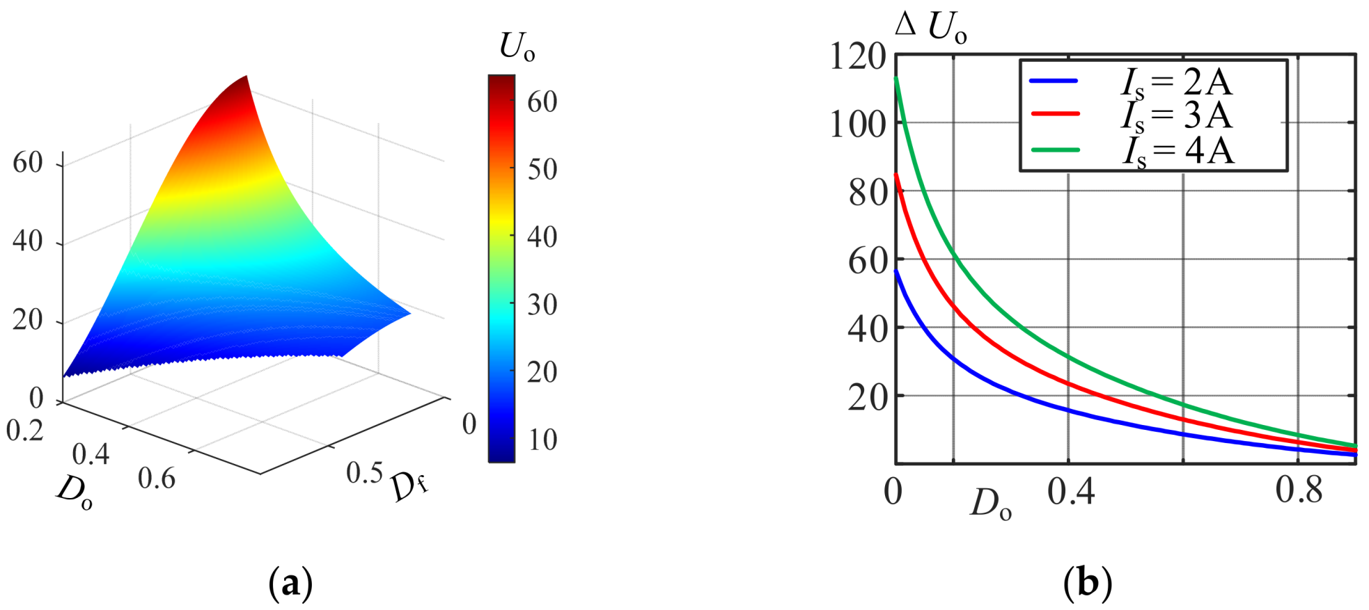
Section 4 analyzes the effects of
Do on output voltage and efficiency.
Section 5 analyzes the small-signal model of the proposed converter.
Section 6 provides experimental validation for the proposed theory.
2. The RHPz Phenomenon and Its Causes of Formation
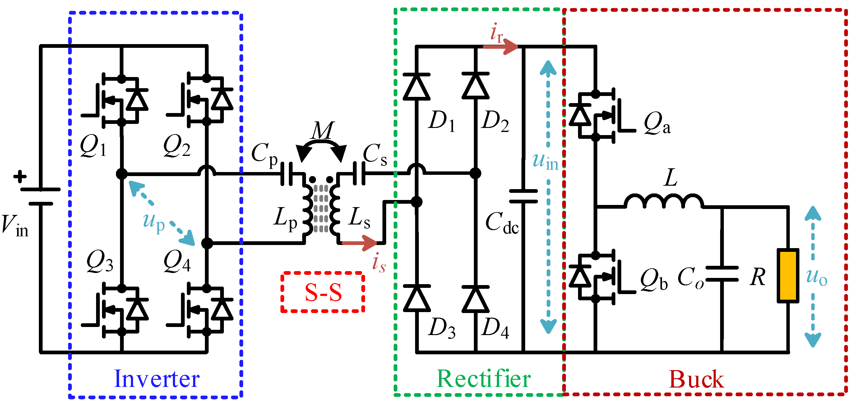
Figure 1 illustrates a typical constant-current WPT system employing Series–Series compensation. Based on the characteristics of the S–S compensation network, if the output voltage at the transmitting side
up remains constant, the output current of the rectifier circuit
ir is also constant. When the rectifier circuit operates in continuous conduction mode (CCM), the input terminal of the Buck converter can be modeled as an equivalent constant current source,
ir:
Here, Is denotes the peak output current of the receiver-side rectifier bridge. To facilitate the analysis, lowercase variables are used throughout this paper to represent instantaneous values, while uppercase variables denote steady-state values.
The transfer function of the constant-current-fed Buck converter can be expressed as shown in Equation (2). Due to the presence of the RHPz, this control system behaves as a non-minimum phase system, which manifests as a negative undershoot in the time-domain output response.
As illustrated in
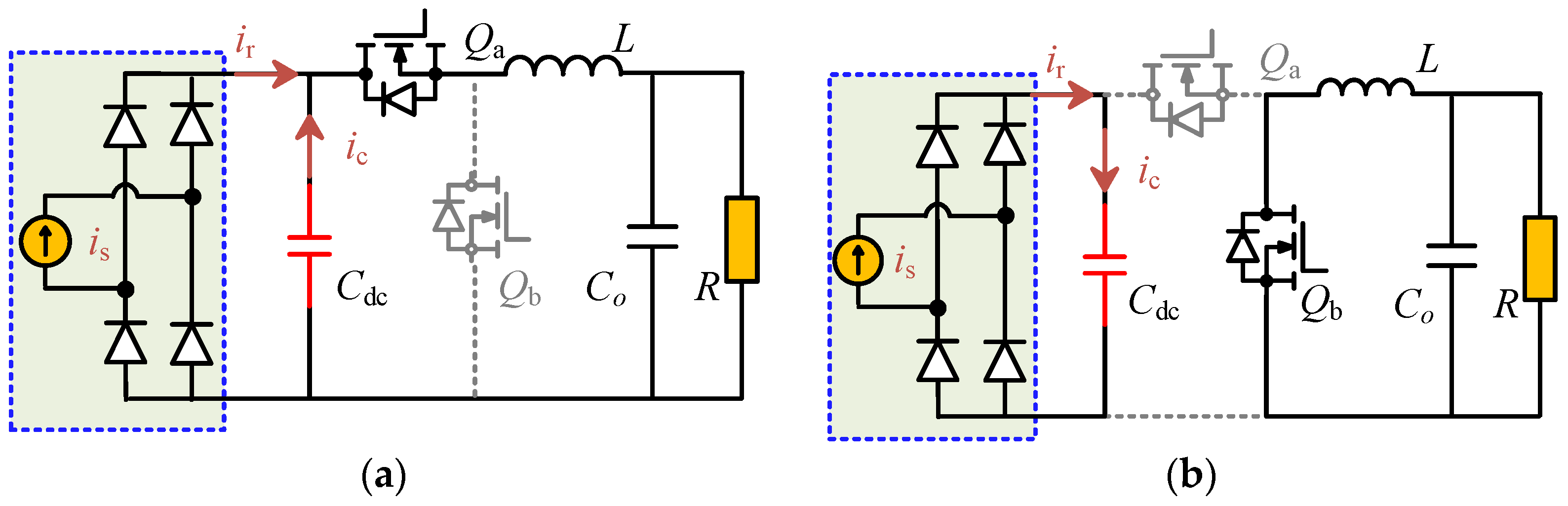
Figure 2, the Buck converter exhibits two distinct operating modes based on the conduction state of switch
Qa and the charge state of the output capacitor
Co. When
Qa is turned on and
Qb is turned off, the operating state of the converter is as depicted in
Figure 2a; during this interval, the input capacitor
Cdc discharges, while the output capacitor
Co charges. Conversely, when
Qa is turned off and
Qb is turned on, the operating state is as shown in
Figure 2b, where
Cdc charges and
Co discharges.
The time-domain manifestation of the RHPz’s effect in a conventional buck converter configured as a constant current source can be characterized as follows. Assuming the desired output voltage increases, the control system must reduce the duty ratio. This adjustment, however, increases the discharge time of the output capacitor, causing the output voltage to dip further until the input capacitor voltage recovers sufficiently to recharge the output capacitor.
3. Analysis of the Proposed Converter Topology
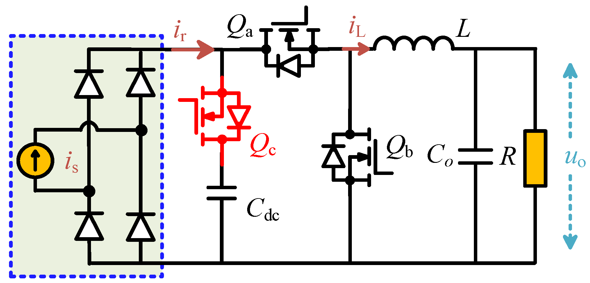
If the discharge time of the output capacitor does not increase alongside the reduction in duty ratio, the negative overshoot phenomenon can be expected to disappear. This observation inspires the introduction of a new state. A novel three-state Buck converter is proposed, which incorporates a switch
Qc in series with the traditional Buck converter input capacitor, as shown in
Figure 3.
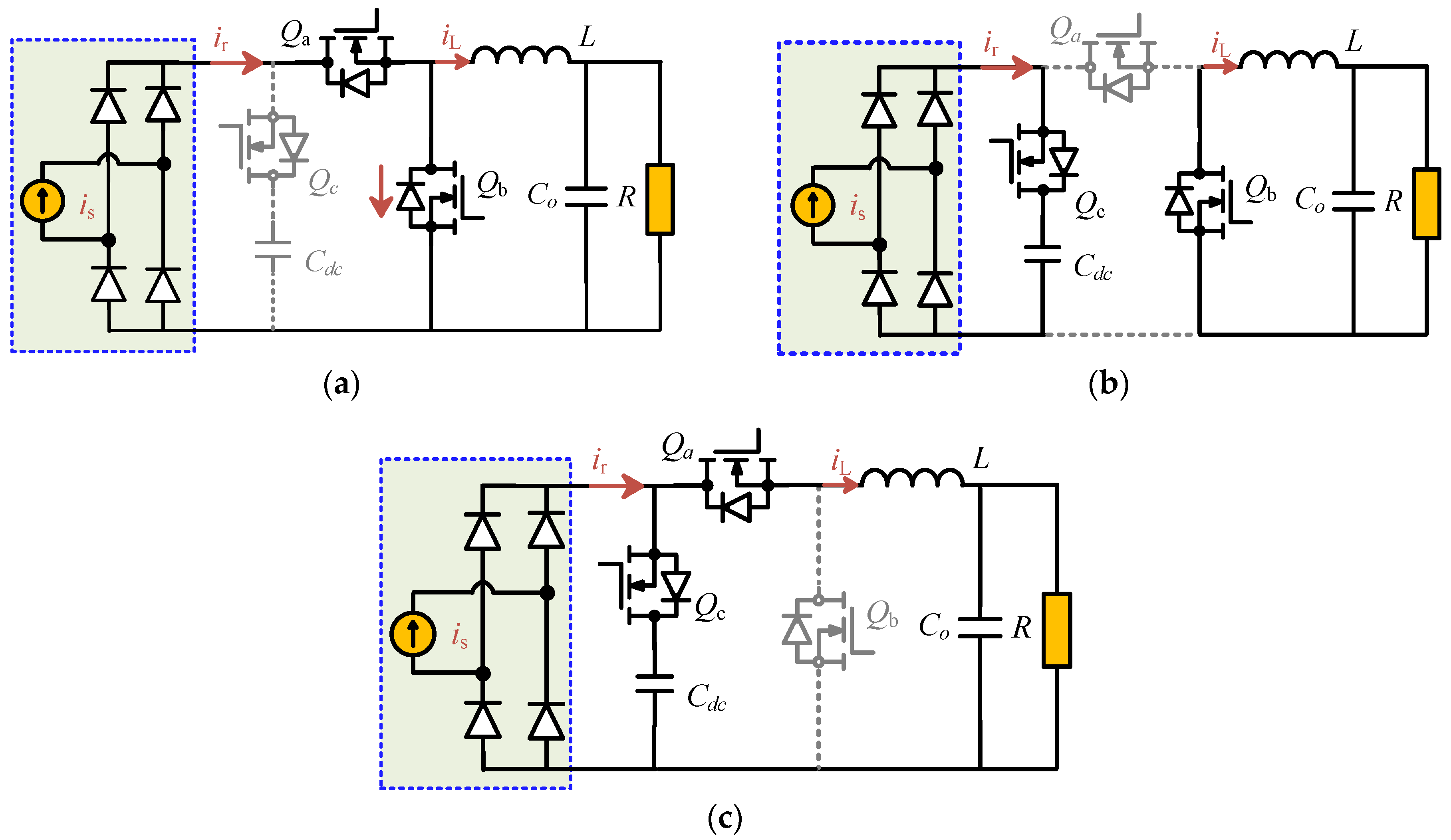
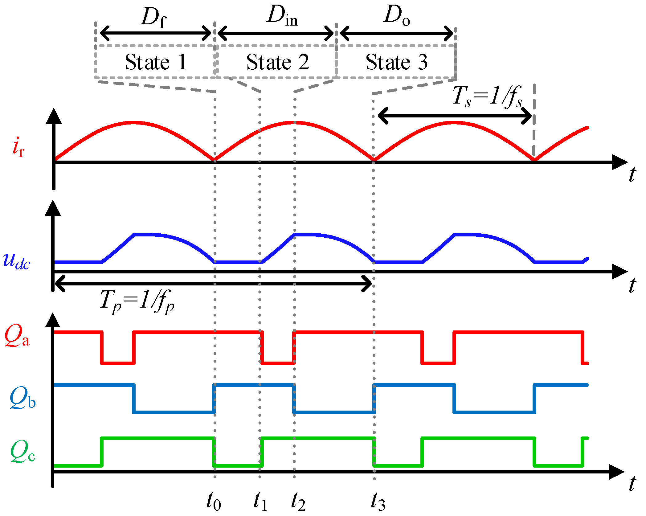
In steady state, the proposed converter operates in three distinct states. These operating states and their corresponding key waveforms are illustrated in
Figure 4 and
Figure 5, respectively.
Figure 4a depicts the “freewheeling state” (State 1), during which switch
Qc is turned off, while
Qa and
Qb are turned on. The current
ir freewheels through
Qa and
Qb. The input capacitor
Cdc is isolated by
Qc, and the output capacitor
Co is in a discharging state.
Figure 4b shows the “
Cdc charging state” (State 2), where switch
Qa is turned off, while
Qb and
Qc are turned on. The current
ir charges the input capacitor
Cdc, and the output capacitor
Co remains in the discharging state.
Figure 4c illustrates the “
Co charging state” (State 3), in which switch
Qb is turned off, while
Qa and
Qc are turned on. During this interval, the input capacitor
Cdc releases energy, while the output capacitor
Co is in a charging state. To facilitate the analysis, the ratios of the durations of these three operating states to the switching period are defined as
Df,
Din, and
Do, respectively. Consequently, the following condition must be satisfied:
The proposed converter introduces an additional freewheeling state (State 1). Subject to the timing constraints, any two operating states in the designed converter can be regulated independently.
Unlike the conventional Buck converter, the charging time of the input capacitor (DinTs) and the charging time of the output capacitor (DoTs) in the proposed converter can be controlled independently. This independent regulation mechanism fundamentally changes the energy transfer process of the converter and prevents an increase in the output capacitor discharging time during duty-cycle variation, thereby eliminating the physical origin of the RHPz. By adjusting the duration of the freewheeling state (DfTs), the proposed converter allows the input capacitor charging time (DinTs) to be regulated without affecting the output capacitor charging time (DoTs), successfully removing the original RHPz and enabling improved dynamic response.
Based on the ampere-second balance of
Cdc and
Co, and the volt-second balance of
L, we can obtain the following:
where
Udc and
Uo denote the input and output voltages, respectively, and
IL represents the inductor current; the output voltage
Uo can be derived as follows:
5. Small-Signal Modeling and Analysis
The proposed converter operates in three distinct states, each defined by the conduction of switches Qa, Qb, and Qc. The state-space equations for each operating state capture the energy transfer dynamics between the input capacitor Cin, the output capacitor Co, and the inductor L By establishing these equations, the dynamic response, stability margins, and the effects of RHPz can be rigorously analyzed, serving as the foundation for subsequent small-signal modeling and controller design.
- 2.
State 2 (Din Ts):
- 3.
State 3 (Do Ts):
By employing the switching-cycle averaging method, the derived switching model is given as follows:
Here, <
udc>
Ts, <
iL>
Ts, and <
uo>
Ts represent the switching-period-averaged input voltage
udc, inductor current
iL, and output voltage
uo over one switching period
Ts, respectively. By introducing low-frequency small-signal perturbations to the averaged variables in Equations (17)–(19), we obtain
where
Udc,
IL,
Uo,
Df, and
Do denote the steady-state values, while
,
,
,
, and
represent the corresponding small-signal AC perturbations. By substituting these variables into Equations (17)–(20), the small-signal model is derived as shown in Equation (21):
Here,
,
. By deriving Equation (21), the transfer function from the duty cycle
df to the output voltage
uo can be obtained as
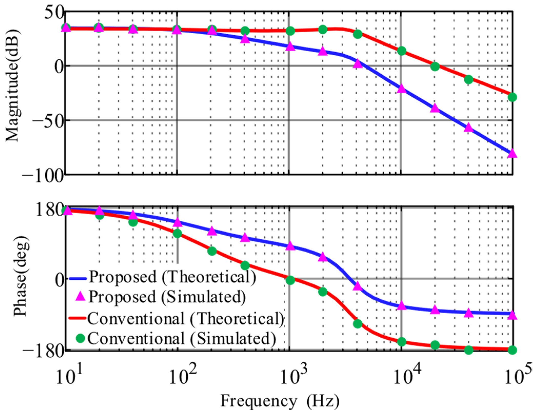
To verify the accuracy of the derived small-signal model, simulation circuits for both the proposed converter and the traditional converter were built using PLECS 5.0.3 software. The simulation results are shown in
Figure 8. The simulation parameters are set as follows:
fs = 170 kHz,
Df = 0.4,
Do = 0.3,
Is = 6 A,
Cdc = 40 μF,
Co = 20 μF,
R = 5 Ω,
L = 220 μH,
D = 0.34. It can be observed that the theoretical predictions and simulation results match well, thereby verifying the correctness of the derived small-signal model. It should be noted that the above small-signal model is idealized and does not explicitly account for parasitic elements such as ESR, ESL, and switching delays. In practice, these parasitics may introduce minor deviations in the dynamic response; however, they do not reintroduce an RHPz, and the fundamental elimination of the RHPz by the proposed topology remains effective.
Furthermore,
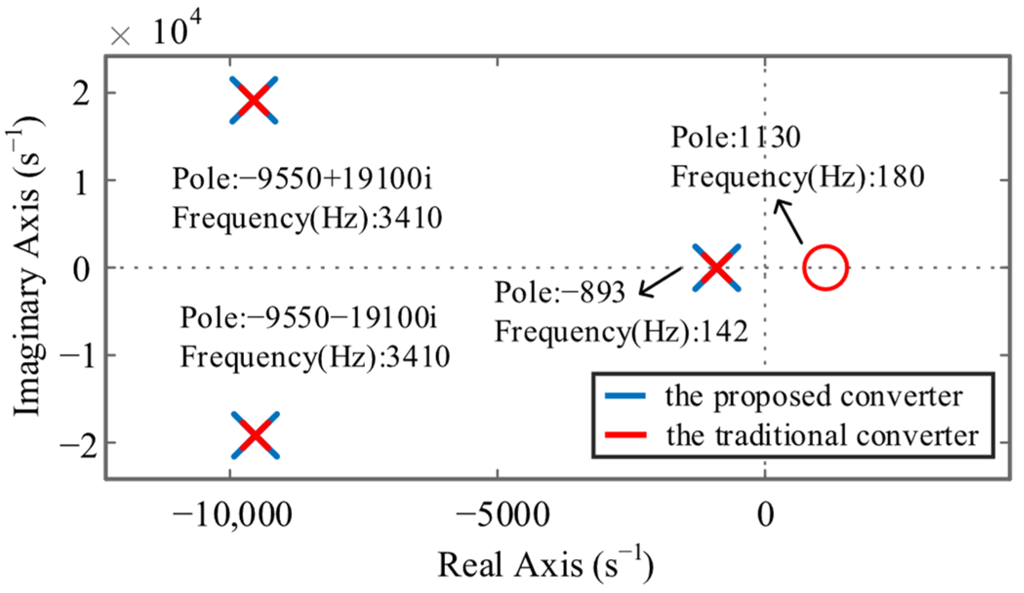
Figure 9 illustrates the pole-zero maps of the two converters, clearly showing that the transfer function of the proposed converter does not contain any RHPZ. As depicted in
Figure 8, the traditional Buck converter exhibits a phase delay of 180° at 1 kHz, whereas the proposed converter only has a delay of 100°. This indicates that the RHPZ in the traditional converter introduces significant phase delay, making its controller more difficult to design and limiting its maximum achievable bandwidth compared to the proposed converter.
6. Experimental Results
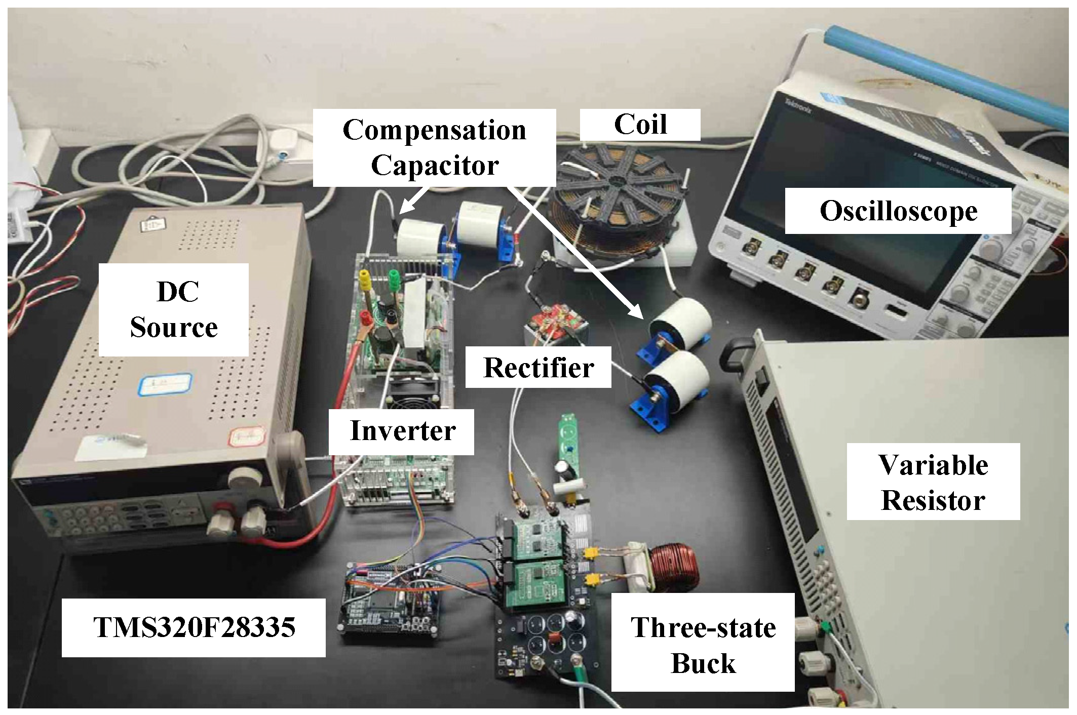
To validate the theoretical analysis, an experimental prototype was developed, as shown in
Figure 10. The platform comprises a DC power supply, inverter, coils, compensation capacitors, an uncontrolled bridge rectifier, a DC–DC converter, and an output load (parameters in
Table 2). A TMS320F28335 DSP is utilized as the controller to implement output-voltage sampling, PI closed-loop control, and PWM signal generation.
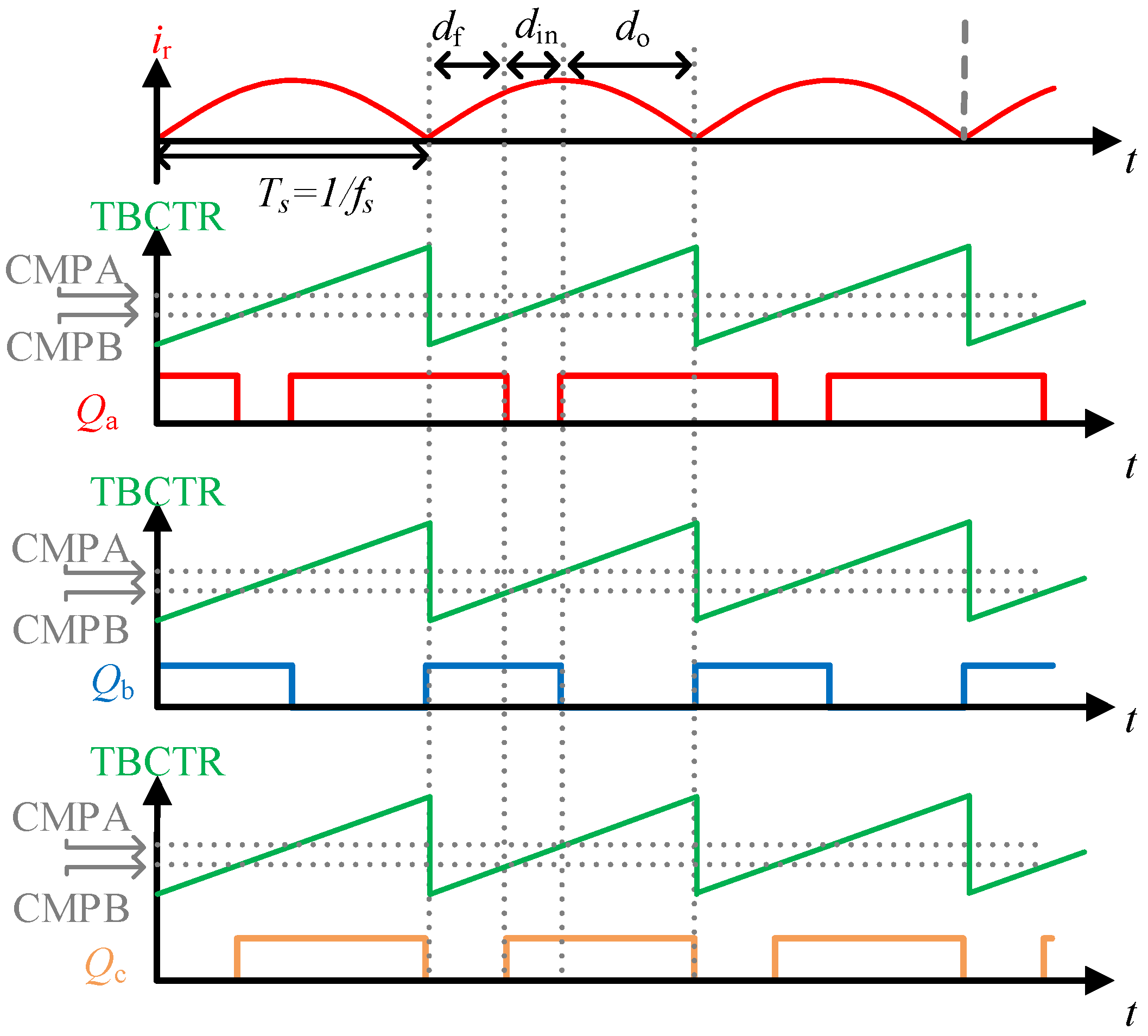
The specific operating modes of each PWM module are summarized in
Figure 11. The PWM1, PWM2, and PWM3 modules of the DSP are utilized to generate the driving waveforms for switches
Qa,
Qb, and
Qc, respectively. The time-base submodules of all three PWM modules are configured in an up-counting mode. To ensure phase synchronization, all modules are triggered to start counting at the zero-crossing point of the input current
ir. The PWM period is determined by the period register (TBPRD), while the duty cycles
Do and
Df are configured via the compare registers CMPA and CMPB, respectively.
6.1. Steady-State Performance
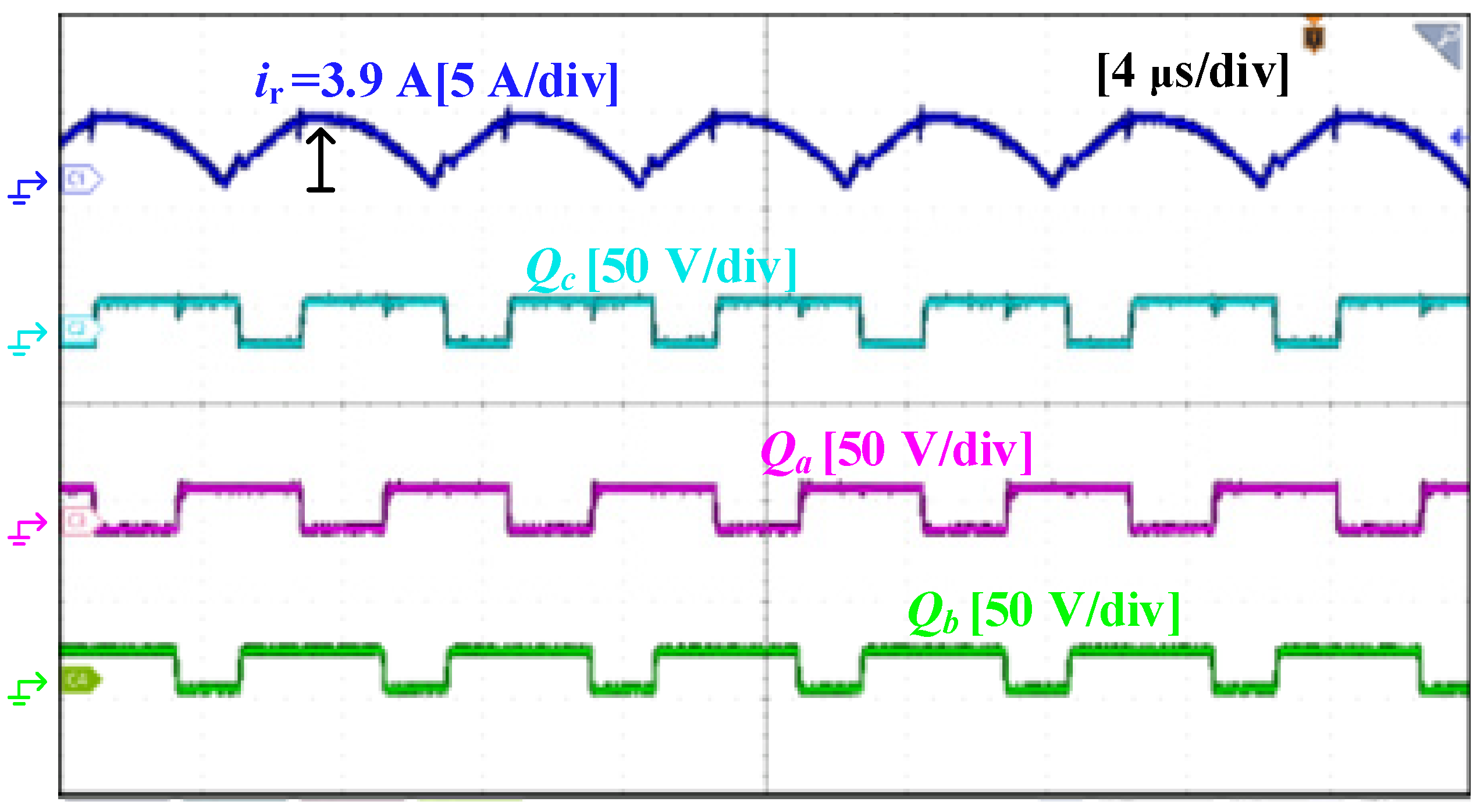
Figure 12 illustrates the key operating waveforms of the designed converter under steady-state conditions, including the input current
ir and the driving signals for switches
Qa,
Qb, and
Qc. Under experimental conditions, the input current exhibits a sinusoidal half-wave characteristic with an amplitude of 3.9 A. The equivalent load is set to
R = 5 Ω, with duty cycles configured as
Df = 0.3 and
Do = 0.3. The experimental results show an output voltage
Uo of 33 V and an output current
Io of 6.7 A. According to the theoretically derived expressions, the calculated output voltage is 33.7 V, which is in close agreement with the measured value of 33 V, thereby verifying the accuracy of the theoretical model.
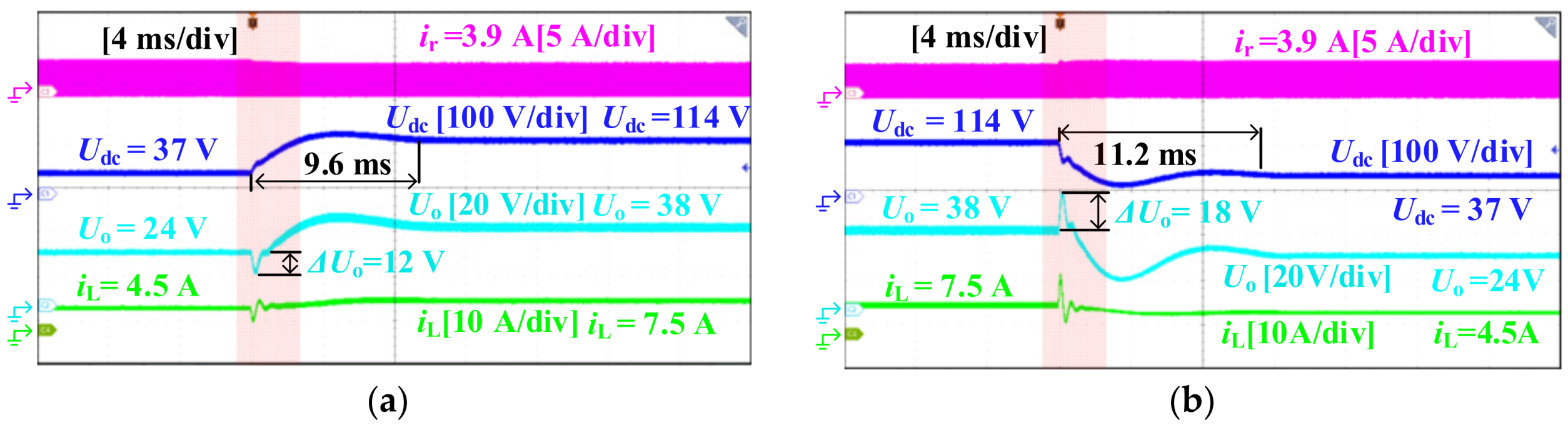
Figure 13 shows the waveforms of input current
ir, input voltage
Udc, inductor current
IL, and output voltage
Uo for a conventional Buck converter during step changes in duty cycle
D. When
D decreases from 0.6 to 0.35, the output voltage
Uo increases from 24 V to 38 V, during which a distinct negative undershoot of 12 V is observed. When
D increases from 0.35 back to 0.6,
Uo drops from 38 V to 24 V, with a more pronounced negative undershoot reaching 18 V. These experimental phenomena clearly reveal the dynamic response deficiencies of the conventional Buck converter under sudden duty cycle variations, particularly the negative undershoot issue caused by the RHPz.
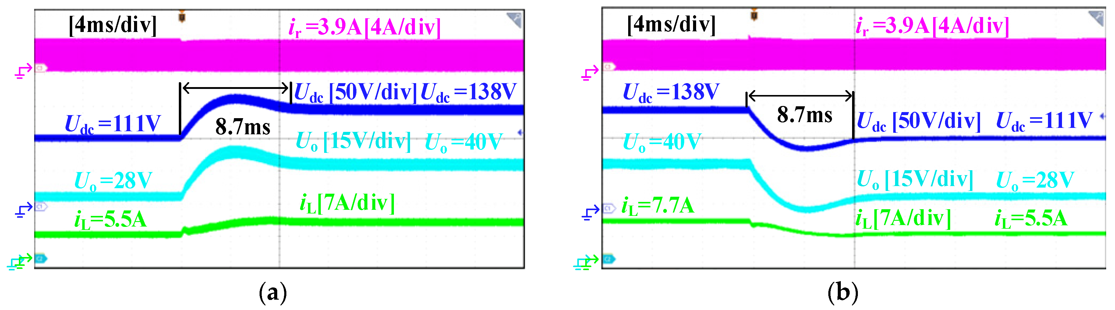
Figure 14 illustrates the waveforms of the input current
ir, input voltage
udc, inductor current
iL, and output voltage
uo for the proposed converter during step changes in duty cycle
Df. When
Df decreases from 0.3 to 0.15, the output voltage
uo increases from 28 V to 40 V. Conversely, when
Df increases from 0.15 back to 0.3,
uo drops from 40 V to 28 V. The experimental results show that the output voltage tracks the reference smoothly, with the deviation remaining below 1 V throughout the transitions.
6.2. Closed-Loop Experiments
To comprehensively evaluate the dynamic performance of the designed converter,
Figure 15 presents the closed-loop control block diagram of the system. In this diagram,
Go,f(
s) represents the open-loop transfer function from the duty cycle
df to the output voltage
uo:
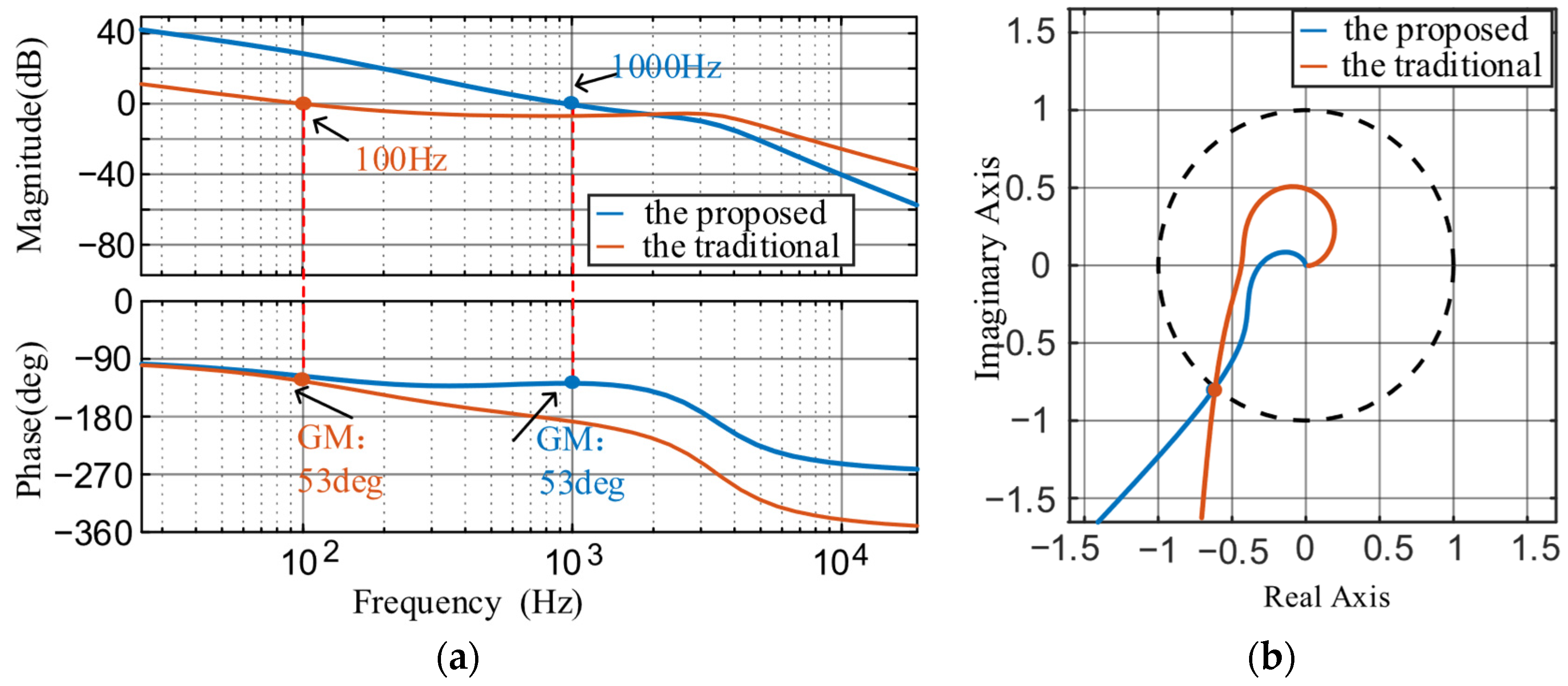
To fully compare the control performance improvement of the proposed converter relative to the conventional Buck converter, the controller parameters are tuned such that both converters maintain a phase margin of 53°. In this case, the crossover frequency of the proposed converter is 1 kHz, with closed-loop parameters
kp = 0.11 and
ki = 395. In contrast, the crossover frequency of the conventional Buck converter is only 100 Hz, with control parameters
kp = 0.004 and
ki = 5.1. The Bode plots of both converters are shown in
Figure 16a, while
Figure 16b presents their Nyquist plots. It can be observed that the stability of the proposed converter is significantly superior to that of the conventional Buck converter.
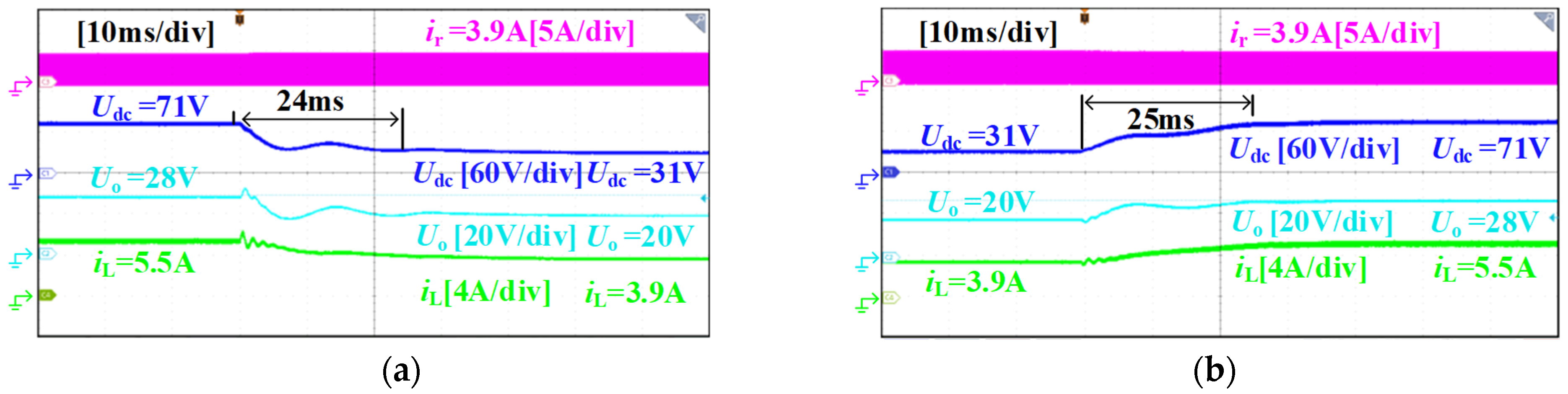
The conventional Buck converter shows settling times of 24–25 ms with a negative undershoot of 20–28 V under step changes, while the proposed converter achieves 4 ms without significant undershoot, as shown in
Figure 17. In contrast, the proposed Buck converter demonstrates significant advantages: It not only reduces settling time by over 83% (from 24/25 ms to 4 ms), but, more importantly, it completely eliminates negative undershoot, achieving fast and smooth voltage regulation. The comparison demonstrates improved dynamic response and stability, with settling time reduced from 24 to 25 ms to 4 ms. A performance boost is primarily attributed to the innovative topology and optimized control strategy that effectively suppresses the adverse effects of the RHPz.
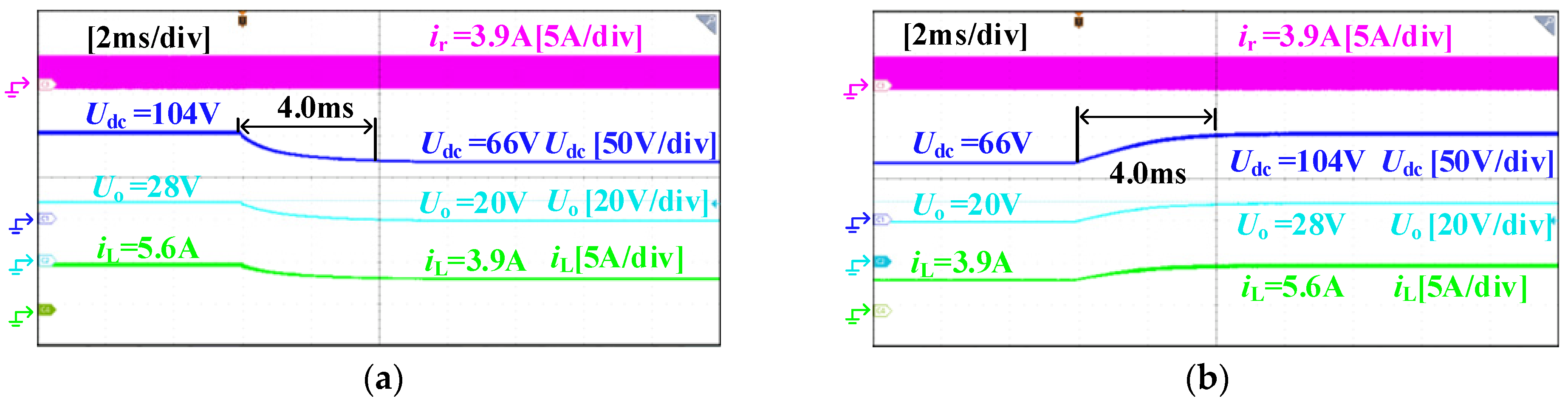
Figure 18 illustrates the closed-loop experimental waveforms of the proposed converter.
Figure 18a displays the dynamic response characteristics when the output voltage reference steps down from 28 V to 20 V, showing a settling time of 4 ms.
Figure 18b shows the dynamic response when the reference steps up from 20 V to 28 V, with a consistent settling time of 4 ms. Compared to the conventional Buck converter, the converter designed in this study demonstrates significant advantages: it not only shortens the settling time but, more importantly, completely eliminates the negative undershoot, achieving rapid and smooth voltage regulation. This comparison fully validates the superiority of the proposed converter in terms of dynamic response speed and stability. The performance enhancement is primarily attributed to the innovative topology and optimized control strategy, which effectively suppress the adverse effects of the RHPz.
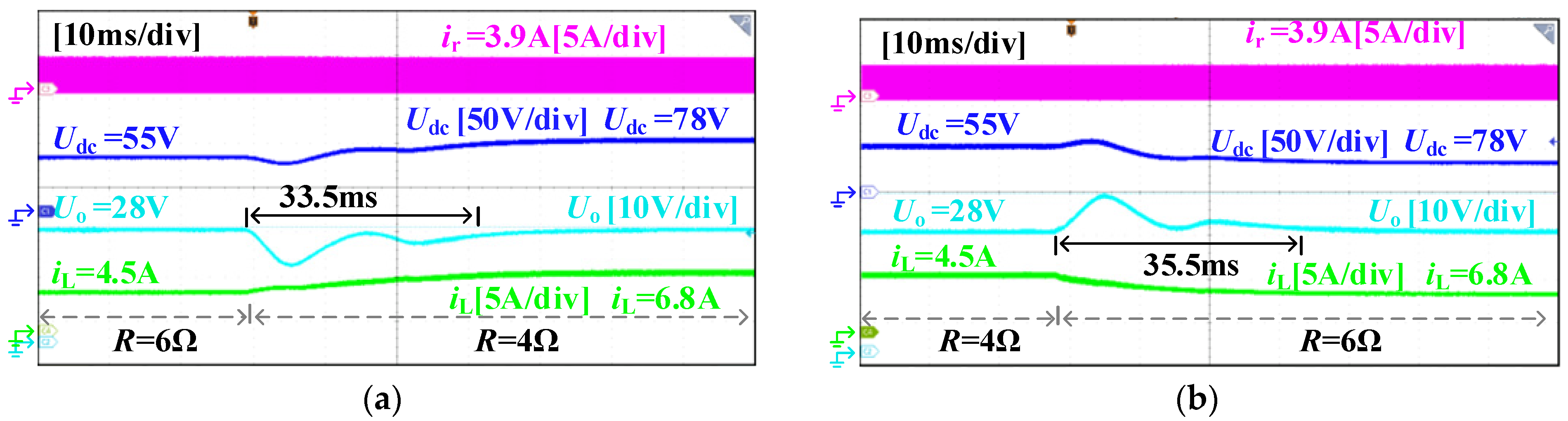
Figure 19 illustrates the dynamic response characteristics of the conventional Buck converter under closed-loop control during load transients. As shown in
Figure 19a, with an output voltage reference of 28 V, when the load
R decreases from 6 Ω to 4 Ω, the system requires 33.5 ms to recover to steady state, during which a transient voltage dip of 8 V is observed. Similarly,
Figure 19b shows that when the load
R increases from 4 Ω to 6 Ω, the settling time is 35.5 ms, accompanied by a significant overshoot of 10 V.
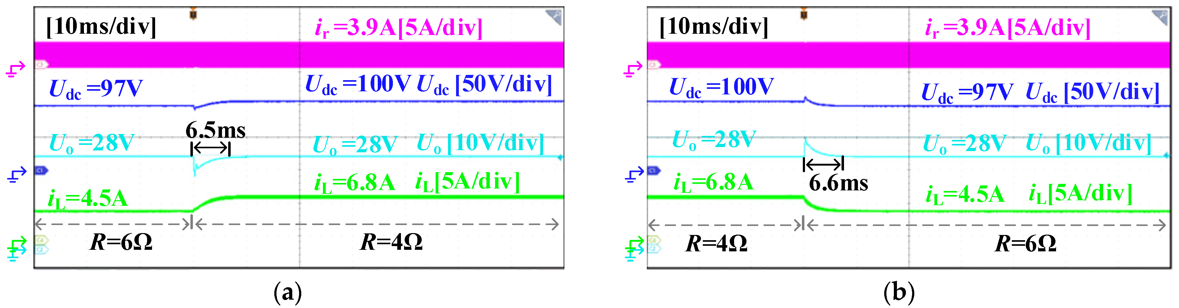
Figure 20 illustrates the dynamic response characteristics of the proposed Buck converter under closed-loop control during load transients. As shown, at an output voltage reference of 28 V, when the load
R decreases from 6 Ω to 4 Ω, the system requires only 6.5 ms to recover to steady state, and the transient voltage dip is maintained within 6 V. Similarly, when the load
R increases from 4 Ω to 6 Ω, the settling time is merely 6.6 ms, accompanied by a slight overshoot of 6 V. These results show that under load transients, the proposed converter recovers to steady state within 6.5–6.6 ms with overshoot less than 6 V, indicating enhanced disturbance rejection and stability.
6.3. Efficiency Analysis
With the output current
Io maintained at a constant 4 A, the load resistance
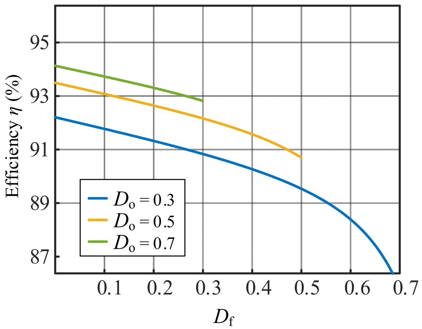
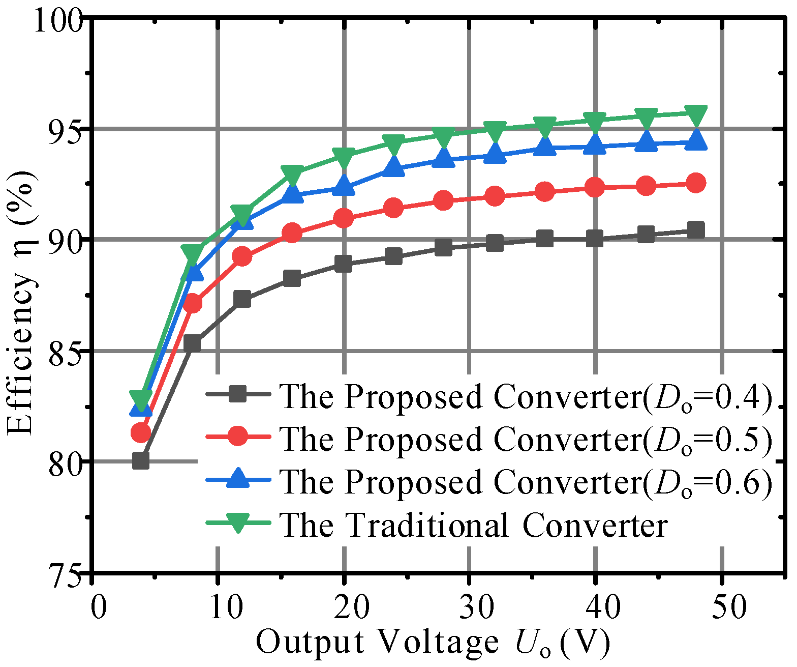
R was adjusted from 1 Ω to 12 Ω using a programmable electronic load. A HIOKI PW8001 power analyzer (HIOKI, Shanghai, China) was employed to conduct a comparative efficiency test between the conventional Buck converter and the proposed converter, with the results shown in
Figure 21. By analyzing the efficiency curves under various duty cycles
Do, it is observed that the system efficiency tends to increase as
Do rises under the same output current conditions, which aligns with the theoretical analysis. Notably, due to the introduction of additional switching tubes and a freewheeling operation state, the efficiency of the proposed converter is slightly lower than that of the conventional Buck converter. Future research could further enhance the efficiency performance by incorporating soft-switching techniques and optimized control strategies.
7. Conclusions
This paper investigates the RHPz issue in conventional constant-current-sourced Buck converters. By incorporating an additional active switch in series with the input capacitor, a novel topology is proposed that fundamentally eliminates the system’s inherent RHPz and significantly enhances both stability and dynamic response. Experimental results demonstrate that the proposed converter achieves a wider closed-loop bandwidth under identical stability margins, and its dynamic response under load disturbances is markedly faster than that of conventional topologies.
Despite these improvements, several limitations remain. The introduction of the additional active switch and the freewheeling operating state leads to a slight reduction in converter efficiency and a marginal increase in switching-related losses. The increased switching transitions may also introduce electromagnetic interference (EMI) challenges in high-power applications.
Nevertheless, the proposed topology offers promising opportunities for future WPT systems requiring fast dynamic response, high stability, and flexible control. Future work will focus on integrating soft-switching techniques, such as zero-voltage switching (ZVS) or zero-current switching (ZCS), optimizing switch timing and control strategies, and extending the concept to higher-power and bidirectional WPT applications. These approaches are expected to further reduce switching losses, improve overall efficiency, and maintain robust RHPz elimination under practical operating conditions.