Article

A Double Closed-Loop Steady-State Error Compensation Strategy for Grid-Forming Converters Using the Deadbeat Predictive Control Technique

Jiangsu Electric Power Testing and Research Institute Co., Ltd., Nanjing 211103, China
*
Author to whom correspondence should be addressed.
Energies 2026, 19(14), 3255; https://doi.org/10.3390/en19143255
Submission received: 5 June 2026 / Revised: 6 July 2026 / Accepted: 7 July 2026 / Published: 10 July 2026
(This article belongs to the Section A1: Smart Grids and Microgrids)

Abstract

The deadbeat predictive control (DPC) method has received increasing research interest in the grid-forming converter control strategy, due to its advantages of fast response in emergency grid scenarios and great potential in utilizing a system multi-time-step predictive optimization strategy. However, the voltage–current double-loop DPC of a grid-forming converter is sensitive to the filter inductance and capacitance parameters, resulting in a steady-state tracking error under parameter mismatch conditions. To address this issue, this manuscript proposes a double closed-loop steady-state error compensation strategy for grid-forming converters using double-loop DPC. Based on an analysis of the DPC algorithm and the mechanism of performance degradation caused by parameter mismatch, compensation terms are designed for the inner current loop and outer voltage loop respectively. The compensation terms are constructed from the feedback errors, effectively and rapidly suppressing the performance degradation caused by parameter mismatch, without introducing complex observers that may degrade the system dynamic response speed. A simulation model, which includes both the physical model of the electrical circuit and the discrete-time controller with sample-and-hold characteristics, is established to verify the proposed control strategy under different operating conditions, including load transient and inductor parameter mismatch. The results demonstrate that the proposed compensation method significantly reduces the steady-state tracking error caused by parameter mismatch while preserving the fast dynamic response characteristic of DPC, thereby substantially improving the accuracy of active power output and enhancing the system’s robustness against parameter deviations.

1. Introduction

With the continuous expansion of the renewable energy generation scale, the equivalent inertia and damping level of the power grid are continuously decreasing. Grid-forming (GFM) technologies, such as Virtual Synchronous Generator (VSG), simulate the electromechanical transient characteristics of synchronous generators, endow grid-connected converters with the functions of inertia response and primary frequency regulation, and have become an important technical approach to improve power grid stability [1,2,3,4,5].
Voltage–current double-loop control is the core part to ensure the stable operation of a GFM converter. In the double-loop control of GFM, the outer voltage loop usually adopts PI or resonant controllers to generate reference commands for the inner current loop, while the inner current loop realizes rapid regulation of grid-connected current or filter inductor current [6,7,8,9]. On the premise of ensuring system stability, how to suppress the performance degradation caused by parameter mismatch is one of the key issues in current GFM control research.
Model predictive control (MPC) is a digital control strategy based on a discretized model. It predicts the response of the plant under specific outputs to find the optimal solution that satisfies the requirements of a cost function. Zheng et al. proposed an improved finite control set MPC-based VSG scheme suitable for islanded AC microgrids, which effectively enhances the system’s dynamic response speed and suppresses the rate of change of frequency [10]. To significantly accelerate the dynamic response and simplify parameter tuning, Zheng et al. suggested replacing the conventional voltage–current double-loop and modulation strategy with MPC [11]. Liu et al. applied a cascaded MPC structure to the inner and outer loops of primary control to enhance the system’s frequency regulation capability [12]. Guo et al. adopted a weighted voltage model predictive control with online adjustment of weighting coefficients to improve robustness against variations in inductance and capacitance parameters [13].
Deadbeat predictive control (DPC) has been widely studied due to its theoretically optimal dynamic response. This method relies on an accurate model of the plant and can achieve overshoot-free tracking of the reference within two sampling periods, offering advantages such as fast dynamic response, high control accuracy, and constant switching frequency [14]. In recent years, DPC has been widely applied in three-phase grid-connected converters, active power filters, and motor drive systems, with particularly significant advantages in fast current response scenarios [15,16,17]. However, the performance of DPC heavily depends on the accuracy of the model parameters, especially inductance and capacitance. In practical applications, filter inductance is susceptible to deviations from nominal values due to factors such as magnetic saturation, temperature drift, and manufacturing tolerances, leading to current prediction errors, which cause current tracking errors and may even endanger system stability in severe cases [18]. For voltage–current double-loop control, inductance and capacitance mismatch will introduce errors into the system cross-coupling terms, resulting in steady-state tracking errors.
To address the above issues, various improved compensation schemes have been proposed in existing studies. Yu et al. adopted an observer for online estimation and disturbance compensation in an interleaved Boost converter, achieving zero steady-state tracking error [19]. Huang et al. proposed a model-free predictive control for GFM with VSG, which fundamentally avoids the parameter mismatch problem [20]. However, such methods generally suffer from drawbacks such as degraded dynamic response, complicated parameter tuning, and high computational burden.
In summary, the GFM double closed-loop control imposes high demands on the dynamic performance and parameter robustness of the inner current loop. Although DPC offers excellent dynamic response characteristics, its performance is significantly affected by inductance parameter mismatch, which limits its engineering application in grid-connected converters. To address this issue, inspired by the single-loop steady-state error compensation method for permanent magnet synchronous motor drive systems, this manuscript proposes a voltage–current double closed-loop steady-state error compensation strategy for GFM converters, in order to enhance the parameter robustness of the control algorithm. This method does not require the introduction of various disturbance observers, which will have a negative influence on the dynamic response performance. Instead, it constructs a concise compensation term calculated from the tracking error, effectively eliminating the steady-state tracking error caused by inductance mismatch while preserving the fast dynamic response characteristic of DPC.
The rest of the manuscript is organized as follows. Section 2 presents the fundamental principles of the voltage–current double-loop control strategy for GFM using DPC (GFM-DPC). Section 3 derives the steady-state error compensation terms for the double closed-loop of GFM-DPC. Section 4 validates the effectiveness of the proposed method through simulations under various operating conditions.

2. Voltage–Current Double-Loop Control Strategy for GFM-DPC

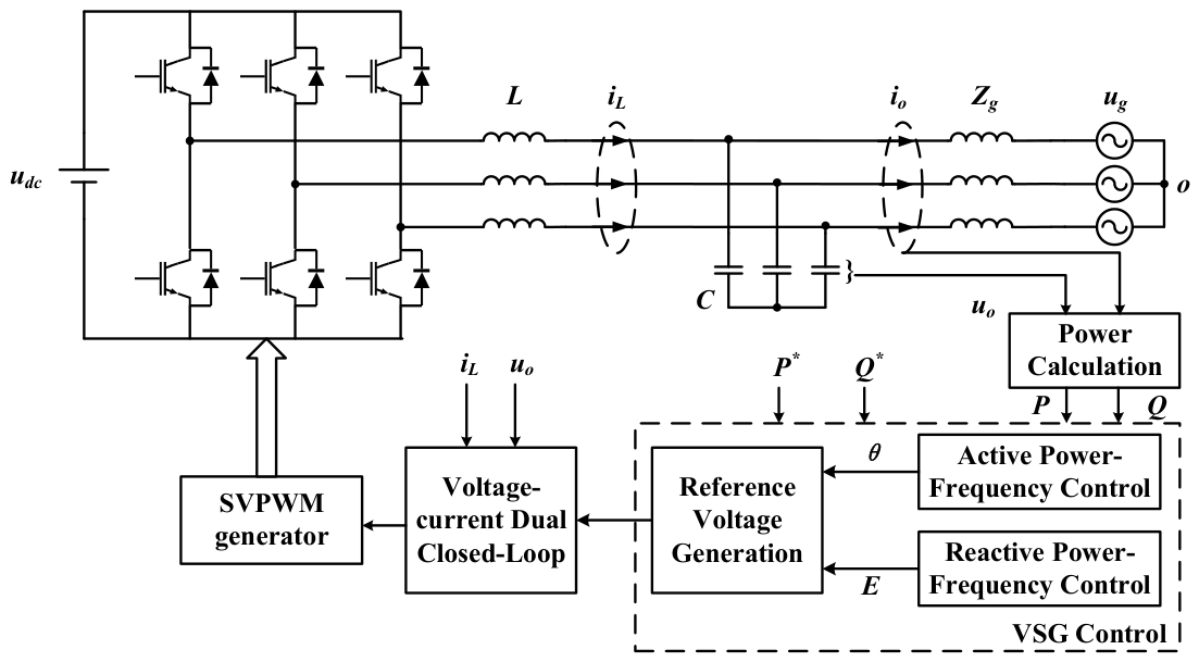
The grid-connected topology of the GFM converter is shown in Figure 1. The instantaneous active and reactive powers are calculated. VSG control is adopted, where the active power control is used to regulate the system frequency/phase angle and the reactive power control is used to regulate the amplitude of the voltage waveforms connected to the grid. Since there is voltage drop over the LC filter, a voltage–current double closed-loop control, including an outer voltage loop and an inner current loop, is utilized to compensate the voltage drop and ensure correct voltage connected to the grid.
According to Kirchhoff’s Current Law (KCL) and Kirchhoff’s Voltage Law (KVL) equations, the time-domain mathematical models of the outer voltage loop and inner current loop can be derived respectively as follows:
{ i L d = C d u o d d t + i o d ω 0 C u o q i L q = C d u o q d t + i o q + ω 0 C u o d ,
{ u d = L d i L d d t + u o d ω 0 L i L q u q = L d i L q d t + u o q + ω 0 L i L d ,
Equation (1) corresponds to the outer voltage loop, and Equation (2) corresponds to the inner current loop, where L is the filter inductor, C is the filter capacitor, uo is the output voltage at the filter port, io is the output current at the filter port, u is the port voltage of the converter, and iL is the inductor current. Considering the output voltage uo and inductor current iL as the system state variables, the time-domain state equations of the system voltage–current double loop in the dq-axis can be obtained respectively:
[ d u o d d t d u o q d t ] = [ 0 ω 0 ω 0 0 ] [ u o d u o q ] + [ 1 C 0 0 1 C ] [ i L d i o d i L q i o q ] [ d i L d d t d i L q d t ] = [ 0 ω 0 ω 0 0 ] [ i L d i L q ] + [ 1 L 0 0 1 L ] [ u d u o d u q u o q ] .
By discretizing the above expressions, the discrete-time mathematical model of the system under the framework of DPC can be derived. The forward difference method is adopted to predict the voltage and current state variables at the next sampling instant. When the system sampling frequency is set sufficiently high and far exceeds the operating frequency of the signal, it can be assumed that each state variable follows a linear variation rule within a single sampling period. Based on this premise, the differential terms of the output voltage and inductor current can be discretized via the forward difference formula.
Taking the d-axis as an example:
{ d u o d d t = u o d ( k + 1 ) u o d ( k ) T s d i L d d t = i L d ( k + 1 ) i L d ( k ) T s ,
where Ts is the sampling period. By implementing forward difference transformation on the differential links of the output voltage and current according to Equation (4), the discrete-time equation of the system on the d-axis can be derived:
u ^ o d ( k + 1 ) = u o d ( k ) + T s [ 1 C ( i L d ( k ) i o d ( k ) ) + ω 0 u o q ( k ) ] ,
i ^ L d ( k + 1 ) = i L d ( k ) + T s [ 1 L ( u d ( k ) u o d ( k ) ) + ω 0 i L q ( k ) ] ,
where variables with the superscript ^ represent estimated values. Equations (5) and (6) realize the prediction of state variables at the next sampling instant (i.e., instant k + 1) via the forward difference method. The objective of DPC is as follows: when the change in the reference value of the controlled state variable is detected at instant k, the control output for the next control period (the time interval between instant k + 1 and k + 2) is calculated based on the controlled plant model, so that the controlled state variable reaches its reference value at instant k + 2. It should be particularly emphasized that in the digital control system, the voltage output command calculated in the current control period cannot take effect immediately. It can only be updated to the duty cycle of the power device in the next period, which introduces a delay of one sampling period. Therefore, the output of the current control period is calculated and determined in the previous control period, which is also the reason why Equations (5) and (6) can predict the state variables at the next sampling instant (i.e., instant k + 1) based on the output of the current control period.
Based on the system state at instant k + 1, the system state at instant k + 2 can be predicted by the following equation:
u ^ o d ( k + 2 ) = u ^ o d ( k + 1 ) + T s [ 1 C ( i L d ( k + 1 ) i ^ o d ( k + 1 ) ) + ω 0 u ^ o q ( k + 1 ) ] ,
i ^ L d ( k + 2 ) = i ^ L d ( k + 1 ) + T s [ 1 L ( u d ( k + 1 ) u ^ o d ( k + 1 ) ) + ω 0 i ^ L q ( k + 1 ) ] ,
where u ^ o d ( k + 1 ) and i ^ L d ( k + 1 ) are obtained through prediction via Equations (5) and (6); u ^ o q ( k + 1 ) and i ^ L q ( k + 1 ) can be derived with reference to the q-axis discrete equations similar to Equations (5) and (6); i L d ( k + 1 ) and u d ( k + 1 ) are the state values at instant k + 1.
According to the basic principle of DPC described above, its control objective is to make the actual value of the voltage state variable equal to its reference value at instant k + 2, that is:
u ^ o d ( k + 2 ) = u o d * ( k + 2 ) ,
i ^ L d ( k + 2 ) = i L d * ( k + 2 ) .
Substituting Equation (9) into the outer voltage loop prediction Equation (7), the reference value of the inductor current required for the grid-connected voltage to reach its reference value at instant k + 2 is derived:
i L d * ( k + 1 ) = [ C T s ( u o d * ( k + 2 ) u ^ o d ( k + 1 ) ) ω 0 C u ^ o q ( k + 1 ) ] + i ^ o d ( k + 1 ) .
Similarly, substituting Equation (10) into the inner-current-loop-prediction Equation (8), the reference value of the converter output voltage between instant k + 1 and instant k + 2, which is required for the converter output current to reach its reference value at instant k + 2, is derived:
u d * ( k + 1 ) = [ L T s ( i L d * ( k + 2 ) i ^ L d ( k + 1 ) ) ω 0 L i ^ L q ( k + 1 ) ] + u ^ o d ( k + 1 ) .
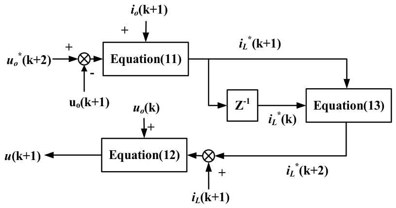
As shown in Equation (11), the outer voltage loop is responsible for providing command reference to the inner current loop, and the voltage reference value output by the controller is derived from the inner-current-loop Equation (12) based on DPC. However, the calculation of the inner current loop in Equation (12) requires the reference value at instant k + 2, so the current reference signal needs to be predicted in advance.
There are two feasible approaches to obtain iL(k + 2). The first is based on the model predictive algorithm in Equation (11): after predicting iL(k + 1), the system state variables such as io(k + 2) and uo(k + 2) are further estimated to predict iL(k + 2). However, this method requires multi-step prediction, which imposes certain limitations on both computational burden and accuracy. The second approach is to directly estimate iL(k + 2) via an extrapolation method, which is simple and fast but may introduce stability risks. To ensure system stability, we adopt the half-cycle extrapolation method as follows [21]:
i L d * ( k + 2 ) = 0.5 i L d * ( k + 1 ) + 0.5 i L d * ( k ) .
The control block diagram of both voltage and current loops adopting DPC is shown in Figure 2:
The reference value of the inductor current at time k + 1, calculated by Equation (11), together with the reference value at time k, is used to extrapolate the reference value at time k + 2, which is then fed into the inner current loop.

3. Steady-State Error Compensation Strategy for Double Closed-Loop Control

DPC has strong dependence on system model parameters. In practical engineering applications, filter capacitors and inductors often deviate from their nominal values due to factors including magnetic saturation, temperature variation and manufacturing error, which causes deviation in current prediction and further induces steady-state current tracking error. In VSG double closed-loop control, the steady-state error of the voltage–current double loop will affect the precise control of output power.
First, the compensation term for the current loop should be designed. Ignoring the effect of resistance, the dq-axis voltage equation of the converter in the synchronous rotating coordinate system can be expressed in complex vector form [21]:
u ¯ d q = L p i ¯ L d q + j ω L i ¯ L d q + u ¯ o d q ,
where the variables with superscript “-” are in complex vector form, p is the differential operator, ω0 is the reference angular frequency, and f can represent voltage or current.
f ¯ d q = f d + j f q .
By discretizing Equation (14), we can obtain:
u ¯ d q ( k ) = β 1 [ i ¯ L d q ( k + 1 ) ( 1 j ω T s ) i ¯ L d q ( k ) ] + u ¯ o d q ( k ) ,
where:
  β = T s L .
Considering the unit calculation delay, the dq-axis current at instant k + 1 needs to be predicted based on the current feedback value at the kth sampling instant:
i ¯ ^ L d q ( k + 1 ) = ( 1 j ω T s ) i ¯ L d q ( k ) + β ^ ( u ¯ d q ( k ) u ¯ o d q ( k ) ) ,
where β ^ is calculated according to the nominal value of the inductor parameter, i ¯ L d q ( k ) and u ¯ o d q ( k ) are the inductor current sampled at the kth instant and the output port voltage of the filter respectively, and u ¯ d q ( k ) is the reference value of the converter port voltage at instant k.
Assuming that the output current i ¯ L d q can track the reference current i ¯ L d q * at instant k + 2, the voltage command applied in the (k + 1)th control period is derived as follows:
u ¯ d q * ( k + 1 ) =   β ^ 1 [ i ¯ L d q * ( k + 2 ) ( 1 j ω T s ) i ¯ ^ L d q ( k + 1 ) ] + u ¯ o d q ( k + 1 ) ,
where i ¯ L d q * ( k + 2 ) is the current command calculated from the output of the outer voltage loop in the k th control period, which is required to be tracked at instant k + 2. When there is a mismatch between the actual value and nominal value of the system parameters, the estimated value of the dq-axis current of the actual system output at instant k + 1 can be derived based on Equation (18):
i ¯ ^ L d q r e a l ( k + 1 ) = ( 1 j ω T s ) i ¯ L d q ( k ) + β ( u ¯ d q ( k ) u ¯ o d q ( k ) ) .
The error between the estimated feedback current i ¯ ^ L d q r e a l and the estimated ideal current i ¯ ^ L d q at instant k + 1 is derived from the following equation:
i ¯ ^ L d q r e a l ( k + 1 ) i ¯ ^ L d q ( k + 1 ) = ( β β ^ ) ( u ¯ d q ( k ) u ¯ o d q ( k ) ) .
Based on Equations (18) and (20), the error between the estimated feedback current i ¯ ^ L d q r e a l ( k + 1 ) and the estimated ideal current i ¯ ^ L d q at instant k + 2 is further derived:
i ¯ ^ L d q r e a l ( k + 2 ) i ¯ ^ L d q ( k + 2 ) = [ ( 1 j ω T s ) i ¯ ^ L d q r e a l ( k + 1 ) + β ( u ¯ d q * ( k + 1 ) u ¯ o d q ( k + 1 ) ) ] [ ( 1 j ω T s ) i ¯ ^ L d q ( k + 1 ) + β ^ ( u ¯ d q * ( k + 1 ) u ¯ o d q ( k + 1 ) ) ] = ( 1 j ω T s ) ( β β ^ ) ( u ¯ d q ( k ) u ¯ o d q ( k ) ) + ( β β ^ ) ( u ¯ d q * ( k + 1 ) u ¯ o d q ( k + 1 ) ) .
It can be seen from Equation (22) that if parameter mismatch exists, steady-state error will inevitably exist between the command current and the feedback current. To eliminate this error, the compensation term is defined as follows:
Δ u ¯ d q ( k + 1 ) = β ^ 1 ( 2 j ω T s ) ( i ¯ L d q ( k ) i ¯ ^ L d q ( k ) ) ,
and then the voltage actually output by the controller to Space Vector Pulse-Width Modulation (SVPWM) is:
u ¯ d q o u t * ( k + 1 ) = u ¯ d q * ( k + 1 ) Δ u ¯ d q ( k + 1 ) .
When the actual system parameters are mismatched, the ideal reference voltage cannot be obtained after the calculated reference voltage is processed by Pulse-Width Modulation (PWM) and applied to the converter. An additional compensation term needs to be added to the voltage command output by the predictive control as the new reference voltage. Therefore, the actual inductor current of the system and the estimated value of the inductor current at instant k + 2 can be rewritten respectively as follows:
i ¯ ^ L d q r e a l ( k + 2 ) = ( 1 j ω T s ) i ¯ ^ L d q r e a l ( k + 1 ) + β ( u ¯ d q o u t * ( k + 1 ) u ¯ o d q ( k + 1 ) ) ,
i ¯ ^ L d q ( k + 2 ) = ( 1 j ω T s ) i ¯ ^ L d q ( k + 1 ) + β ^ ( u ¯ d q o u t * ( k + 1 ) + Δ u ¯ d q ( k + 1 ) u ¯ o d q ( k + 1 ) ) .
Thus, the error between the estimated feedback current i ¯ ^ L d q r e a l and the estimated ideal current i ¯ ^ L d q ( k ) after compensation is added at instant k + 2 can be derived:
i ¯ ^ L d q r e a l ( k + 2 ) i ¯ ^ L d q ( k + 2 ) = ( 1 j ω T s ) ( β β ^ ) ( u ¯ d q o u t * ( k ) u ¯ o d q ( k ) ) + ( β β ^ ) ( u ¯ d q o u t * ( k + 1 ) u ¯ o d q ( k + 1 ) ) ( 2 j ω T s ) ( β β ^ ) ( u ¯ d q o u t * ( k 1 ) u ¯ o d q ( k 1 ) ) .
Assuming that the output voltages of the (k − 1)th, kth and (k + 1)th control periods are equal in steady state, and the current error tends to a constant at this time, it can be considered that the steady-state error between the compensated command current and the feedback current at instant k + 2 is zero.
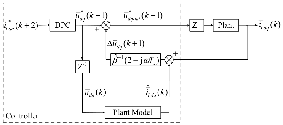
The system diagram of the current loop based on steady-state error compensation can be represented by Figure 3, where the DPC block and the plant model in the controller part use β ^ , while the actual plant uses β .
On this basis, the compensation idea is extended to the outer voltage loop, and the corresponding current command compensation term can be designed in the same way to form a complete double closed-loop error compensation structure. For the outer voltage loop, its dq-axis current equation can also be expressed in complex vector form:
i ¯ L d q = C p u ¯ o d q + j ω C u ¯ o d q + i ¯ o d q .
By discretizing Equation (28), we can obtain:
i ¯ L d q ( k ) =   α 1 [ u ¯ o d q ( k + 1 ) ( 1 j ω T s ) u ¯ o d q ( k ) ] + i ¯ o d q ( k ) ,
where:
α = T s C .
Considering the unit calculation delay, the dq-axis voltage at instant k + 1 needs to be predicted based on the voltage feedback value at instant k:
u ¯ ^ o d q ( k + 1 ) = ( 1 j ω T s ) u ¯ o d q ( k ) + α ^ ( i ¯ L d q ( k ) i ¯ o d q ( k ) ) ,
where α ^ is calculated according to the nominal value of the inductor parameter, u ¯ o d q ( k ) and i ¯ o d q ( k ) are the filter port voltage and output current at instant k respectively, and i ¯ L d q ( k ) is the reference value of the inductor current at instant k.
After two-step prediction, the current command output in the (k + 1) th control period is derived as follows:
i ¯ L d q * ( k + 1 ) =   α ^ 1 [ u ¯ o d q * ( k + 2 ) ( 1 j ω T s ) u ¯ ^ o d q ( k + 1 ) ] + i ¯ o d q ( k + 1 ) ,
where u ¯ o d q * ( k + 2 ) is the voltage command externally input to the outer voltage loop in the kth control period, which is required to be tracked at instant k + 2. Based on Equation (31), the error between the estimated feedback voltage u ¯ ^ o d q r e a l and the estimated ideal voltage u ¯ ^ o d q at instant k + 1 is derived:
u ¯ ^ o d q r e a l ( k + 1 ) u ¯ ^ o d q ( k + 1 ) = ( β β ^ ) ( i ¯ L d q ( k ) i ¯ o d q ( k ) ) .
Through further derivation, the error between the estimated feedback voltage u ¯ ^ o d q r e a l and the estimated ideal voltage u ¯ ^ o d q at instant k + 2 can be obtained:
u ¯ ^ o d q r e a l ( k + 2 ) u ¯ ^ o d q ( k + 2 ) = [ ( 1 j ω T s ) u ¯ ^ o d q r e a l ( k + 1 ) + α ( i ¯ L d q * ( k + 1 ) i ¯ o d q ( k + 1 ) ) ] [ ( 1 j ω T s ) u ¯ ^ o d q ( k + 1 ) + α ^ ( i ¯ L d q * ( k + 1 ) i ¯ o d q ( k + 1 ) ) ] = ( 1 j ω T s ) ( α α ^ ) ( i ¯ L d q ( k ) i ¯ o d q ( k ) ) + ( α α ^ ) ( i ¯ L d q * ( k + 1 ) i ¯ o d q ( k + 1 ) ) .
We add an additional compensation term to the current command:
Δ i ¯ L d q ( k + 1 ) = α ^ 1 ( 2 j ω T s ) ( u ¯ o d q ( k ) u ¯ ^ o d q ( k ) ) ,
and then the actual reference current output to the inner current loop is:
i ¯ L d q o u t * ( k + 1 ) = i ¯ L d q * ( k + 1 ) Δ i ¯ L d q ( k + 1 ) .
Similarly, from this we can obtain the error between the estimated feedback voltage u ¯ ^ o d q r e a l and the estimated ideal voltage u ¯ ^ o d q at instant k + 2:
u ¯ ^ o d q r e a l ( k + 2 ) u ¯ ^ o d q ( k + 2 ) = ( 1 j ω T s ) ( α α ^ ) ( i ¯ L d q o u t * ( k ) i ¯ o d q ( k ) ) + ( α α ^ ) ( i ¯ L d q o u t * ( k + 1 ) i ¯ o d q ( k + 1 ) ) ( 2 j ω T s ) ( α α ^ ) ( i ¯ L d q o u t * ( k 1 ) i ¯ o d q ( k 1 ) ) .
Assuming that the output currents of the (k − 1) th, kth and (k + 1) th control periods are equal in steady state, the steady-state error between the compensated estimated command voltage and the feedback voltage at instant k + 2 is zero.
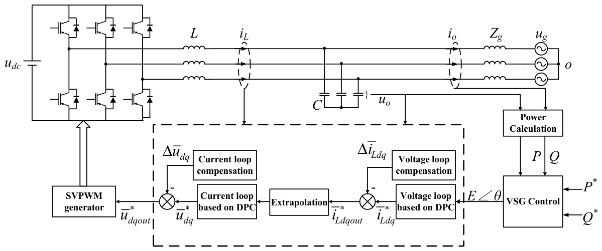
The control block diagram of the double closed-loop steady-state error compensation strategy system for GFM-DPC is shown in Figure 4:
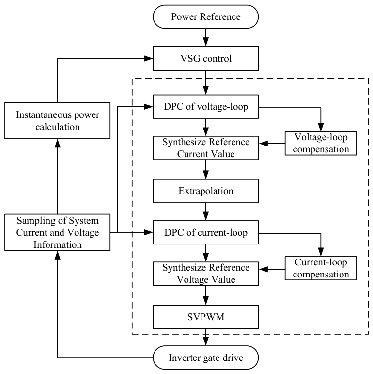
Meanwhile, to more clearly illustrate the execution flow of the proposed control strategy, a flowchart of the control algorithm is provided in Figure 5:

4. Verification

The corresponding model and control loops are constructed based on the above deadbeat double-loop control principle, and the main parameters are listed in Table 1. The simulation model is developed using Matlab R2023b/Simulink. The physical part of the circuit is built with the Specialized Power System blockset from Simscape Electrical, which accurately captures the electrical characteristics of the power electronics circuit. The controller is implemented using a Triggered Subsystem to emulate the discrete-time behavior of a digital controller, with particular attention paid to the one-cycle output delay and the sample-and-hold characteristics, thereby replicating the actual operation of a real digital signal processor (DSP).

4.1. Off-Grid Simulation

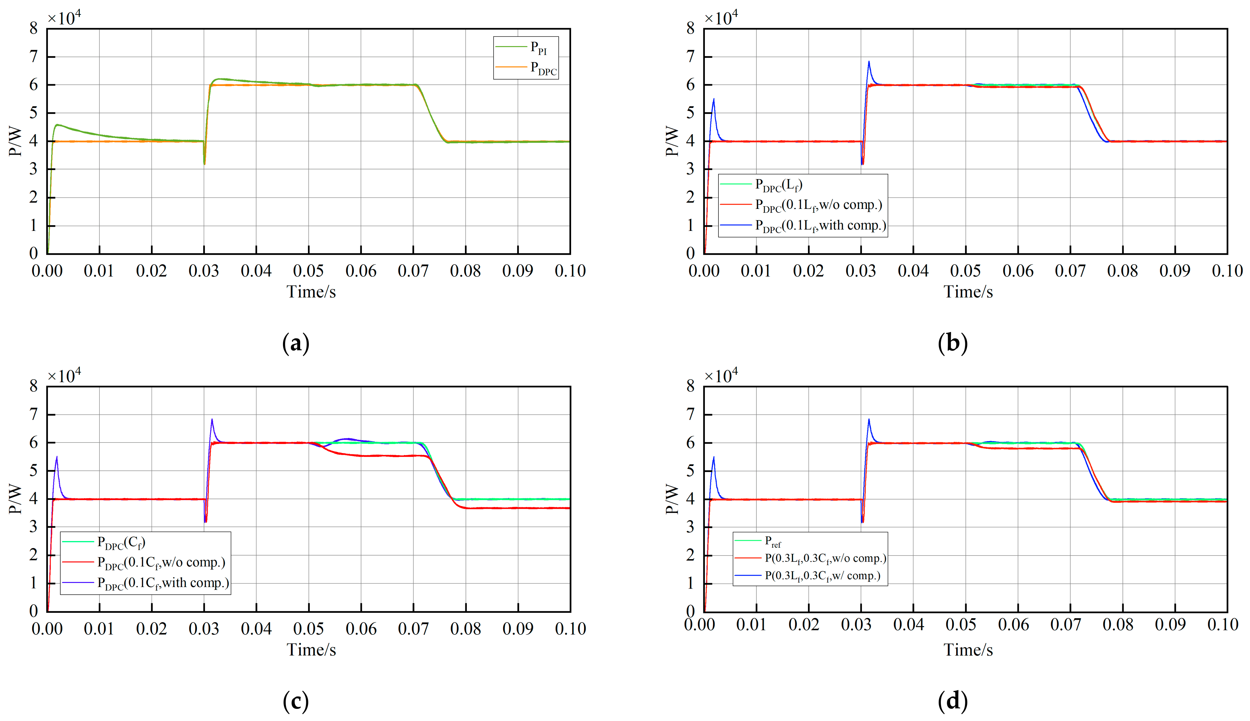
Initially, simulations are carried out in an off-grid environment. To directly observe the double-loop response speed, the reference voltage output part of VSG control is replaced by a waveform generator. The converter initially carries a load of 40 kW. The load suddenly increases to 60 kW at 0.03 s and suddenly decreases to 20 kW at 0.07 s. When simulating parameter mismatch, the estimated values of inductor and capacitor are set to 0.1 times their actual values respectively. The output power of the converter and the current and voltage on the line are observed.
Figure 6 shows the comparison of the system output active power response under different working conditions. Under the load mutation condition, the response speed of the traditional DPC is about 1 ms, which is significantly faster than 20 ms of PI control, reflecting the advantage of fast dynamic response of DPC. After introducing inductor and capacitor parameter mismatch respectively, the output active power has steady-state deviations of about 0.6 kW and 4.7 kW respectively without compensation, and the power tracking accuracy decreases significantly. After adopting the proposed steady-state error compensation strategy, the steady-state deviations of the compensated output active power are reduced to almost 0 kW and 0.1 kW respectively, the power static error is significantly suppressed, and the output power waveform is essentially consistent with that under ideal working conditions. Figure 6d presents the simulation results under simultaneous mismatch of inductor and capacitor parameters. When the estimated values of inductor and capacitor are set to 0.3 times their actual values respectively, the steady-state deviations of the output active power before and after applying the proposed steady-state error compensation strategy are 2 kW and 0.1 kW respectively. The results show that parameter mismatch will impair the power output accuracy of the traditional DPC, while the proposed compensation method can effectively reduce the steady-state error and ensure stable power output.
The above simulations investigate the cases of individual capacitor mismatch and individual inductor mismatch respectively. Considering that the two parameter deviations may occur simultaneously in practice, the estimated values of inductor and capacitor are set to 0.3 times their actual values respectively, and the simulation results under simultaneous mismatch of both parameters are analyzed.
To further investigate the compensation effect of the double loops, the simulation results are observed under the working condition where the estimated values of inductor and capacitor are 0.3 times their actual values respectively.
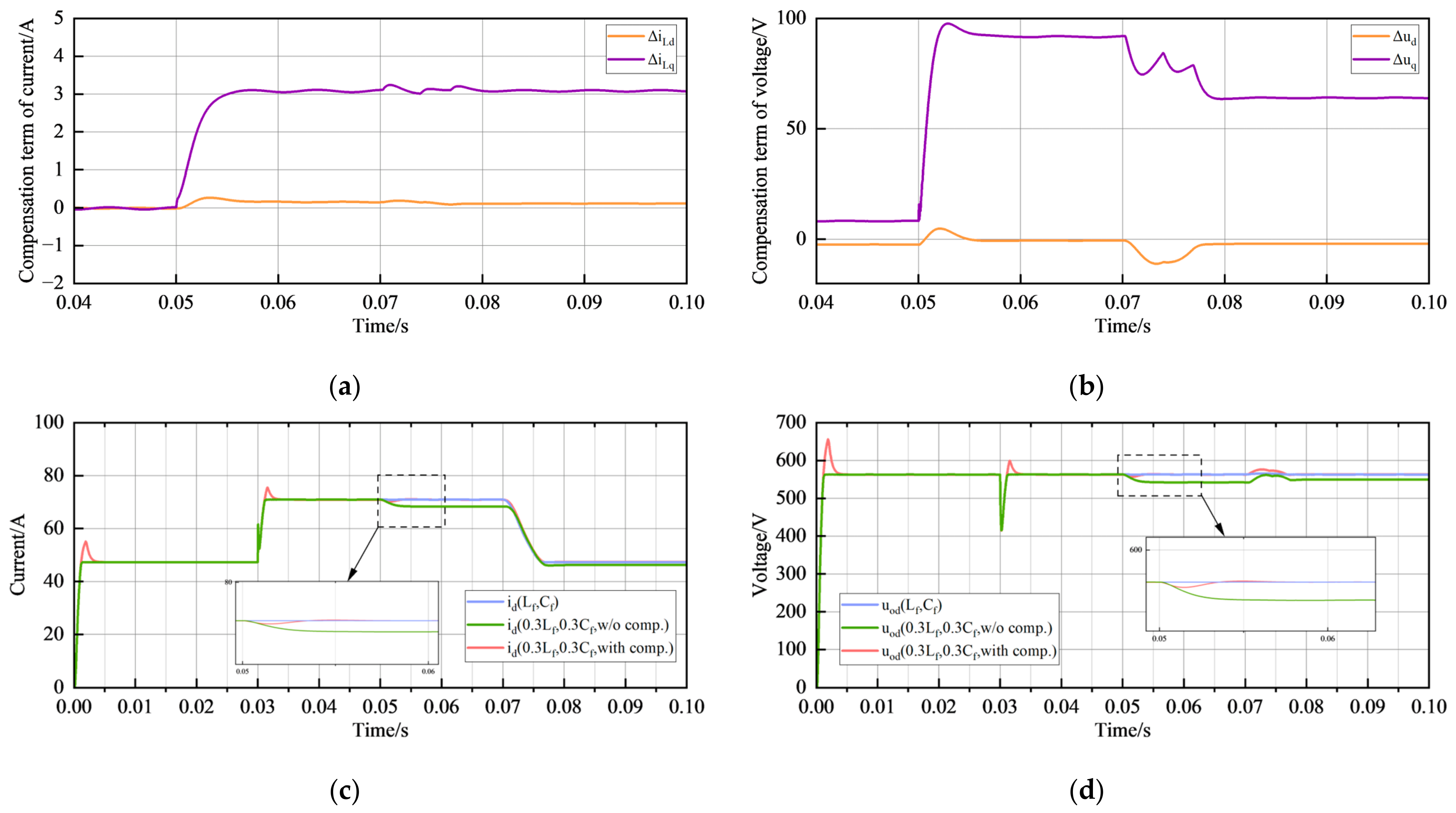
Figure 7 presents the compensation terms of the double closed-loop compensation strategy and the feedback-obtained waveforms under simultaneous mismatch of both capacitor and inductor. In the 0–0.05 s interval without parameter mismatch, the system error is close to zero, and the output of the compensation term is approximately 0. After parameter mismatch occurs at 0.05 s, the compensation terms of the outer voltage loop and inner current loop respond rapidly and output corresponding correction quantities, implementing dynamic compensation for the reference command and control voltage. With error compensation applied, the static error of the d-axis current is essentially eliminated. Compared with the scenario without compensation, the output current recovers to the reference value rapidly within 5 ms. The compensation term has a smooth waveform without severe overshoot, which verifies that the designed compensation strategy can realize adaptive adjustment according to the error magnitude. It can offset the influence of parameter mismatch while maintaining the dynamic stability of the system.

4.2. Grid-Connected Simulation

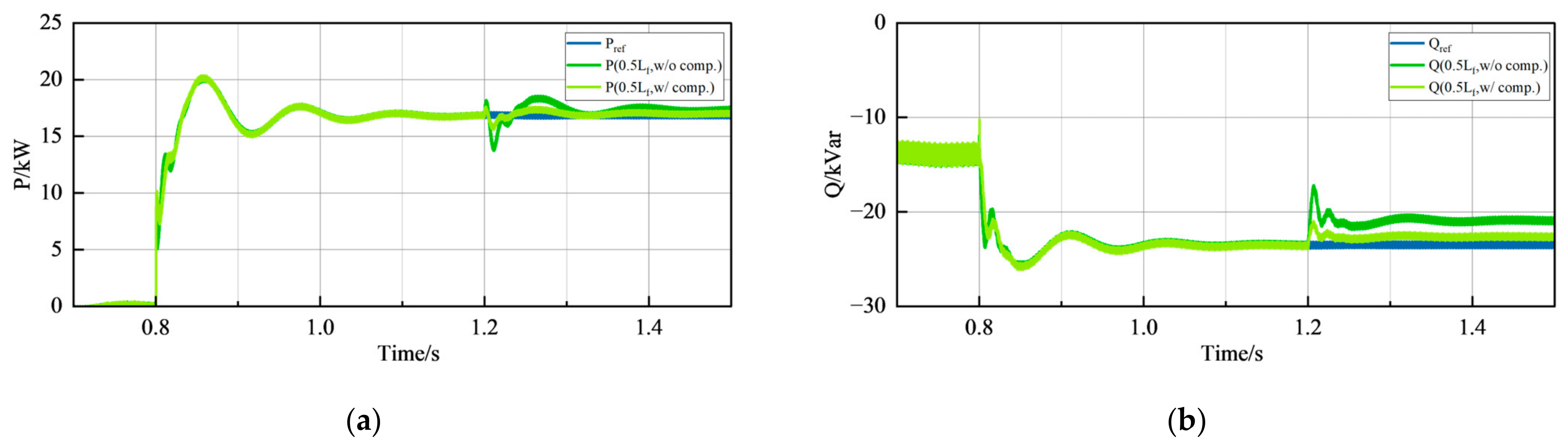
The simulation is conducted in a grid-connected environment, with VSG control adopted for the outer loop to form a VSG-GFM system. The converter is connected to the grid at 0.3 s, and the initial load power on the grid side is balanced. The load increases suddenly by 40 kW at 0.8 s, and the estimated inductor parameter is reduced to 0.5 times its original value at 1.2 s.
Figure 8 shows the active power and reactive power waveforms output by VSG-GFM respectively. When the estimated inductor parameter is reduced at 1.2 s, the output active power of the system under compensated VSG-GFM control can recover to steady state faster than that under uncompensated VSG-GFM control, and the power fluctuation caused by parameter mismatch is reduced. The peak value of active power fluctuation is reduced from 1.8 kW to 0.6 kW, with almost no steady-state error. And the peak value of reactive power fluctuation is reduced from 5.8 kW to 1.9 kW, with a reduction in steady-state error of about 75%.

5. Conclusions

The voltage–current double-loop DPC of GFM is studied in this manuscript, due to its advantages of fast dynamic response in emergency grid scenarios and great potential in utilizing a system multi-time-step predictive optimization strategy. Aiming at addressing the problem that the GFM-DPC is sensitive to the filter inductance and capacitance parameters, which is prone to steady-state errors and deteriorates power output accuracy under parameter mismatch, this manuscript introduces a double closed-loop cooperative steady-state error compensation strategy. Relying on the joint compensation of the outer voltage loop and inner current loop, the performance of DPC is significantly improved. Simulation results demonstrate that under the condition of −70% inductance–capacitance mismatch, the d-axis current static error is essentially eliminated after compensation, and the active power has almost no static error, which greatly improves control accuracy and robustness. Future research would focus on further extension on complex working conditions such as weak grids and multi-machine parallel operation.

Author Contributions

G.Z.: original manuscript, including literature search, design of the work, data collection and analysis; Y.H.: conceptualization and methodology, as well as data interpretation and manuscript review; C.W.: participating in literature search and design of the work, as well as manuscript writing and review. All authors have read and agreed to the published version of the manuscript.

Funding

This research was funded by the Science & Technology Program of Jiangsu Electric Power Testing and Research Institute Co., Ltd., grant number DSY202505.

Data Availability Statement

All data supporting the conclusions are presented in the manuscript. Additional information will be made available by the corresponding author upon request.

Conflicts of Interest

Authors Guojiang Zhang, Yingjie Hu and Chenggen Wang were employed by the company Jiangsu Electric Power Testing and Research Institute Co., Ltd. The authors declare that the research was conducted in the absence of any commercial or financial relationships that could be construed as a potential conflict of interest. The authors declare that this study received funding from Jiangsu Electric Power Testing and Research Institute Co., Ltd. The funder was not involved in the study design, collection, analysis, interpretation of data, the writing of this article or the decision to submit it for publication.

Nomenclature

SymbolDefinitionUnit
udcDC link voltageV
ugGrid voltageV
iLInductor currentA
ioOutput currentA
uInductor voltageV
uoOutput voltageV
LInductanceH
CCapacitanceF
ω0Nominal angular frequencyrad/s
TsSwitching periods
xdd-axis component of the variable
xqq-axis component of the variable
x ¯ d q Vector form of the variable in dq-frame
x*Uncompensated reference value
x ^ Estimated state variable obtained from prediction algorithm using nominal LC parameters
x ^ r e a l Estimated state variable obtained from prediction algorithm using actual LC parameters
Δ u ¯ d q Compensation term for current loopV
u ¯ d q o u t * Compensated reference inductor voltageV
Δ i ¯ L d q Compensation term for voltage loopA
i ¯ L d q o u t * Compensated reference inductor currentA
* Here, the symbol x can represent system variables such as u, u0, iL, and io.

References

  1. Leon, A.E.; del Nozal, Á.R.; Mauricio, J.M. Frequency support strategy for fast response energy storage systems. IEEE Trans. Power Syst. 2024, 39, 5439–5442. [Google Scholar] [CrossRef] [Scilit]
  2. Liu, J.; Yang, D.; Yao, W.; Fang, R.; Zhao, H.; Wang, B. PV-based virtual synchronous generator with variable inertia to enhance power system transient stability utilizing the energy storage system. Prot. Control Mod. Power Syst. 2017, 2, 39. [Google Scholar] [CrossRef] [Scilit]
  3. Li, W.; Ma, M.; Sun, W. Analysis of frequency oscillation characteristics in grid-forming multi-VSG systems considering power coupling. Electr. Power Eng. Technol. 2025, 44, 44–54. [Google Scholar]
  4. Wu, R.; Jiang, Q.; Li, B.; Liu, T. Regional inertia estimation and virtual inertia configuration of new energy connected power system. Electr. Power Eng. Technol. 2026, 45, 3–12. [Google Scholar]
  5. Yang, D.; Li, M.; Ma, T.; Ni, J.; Han, Z. Study on adaptive VSG parameters and SOC control strategy for PV-HESS primary frequency regulation. Energy 2025, 314, 133909. [Google Scholar] [CrossRef] [Scilit]
  6. Zhang, S.; Zhao, J.; Liu, K.; Shi, Z.; Jin, L. Stability enhancement and discrete-time resonant controller synthesis for voltage-controlled voltage source converters. IET Gener. Transm. Distrib. 2022, 16, 924–937. [Google Scholar]
  7. Yang, J.; Zhang, X.; Yang, Z.; Rong, F. A data driven model-free predictive current control for grid-connected inverters. Electr. Power Eng. Technol. 2025, 44, 197–206. [Google Scholar]
  8. Sun, K.; Yao, W.; Zong, Q.; Wen, J.; Jiang, L. Feasible coefficient region analysis and dual-loop adaptive feedback control for transient stability of VSG under severe grid voltage sag. IEEE Trans. Power Syst. 2024, 39, 6127–6143. [Google Scholar] [CrossRef] [Scilit]
  9. Wang, Z.; Pan, G.; Yuan, Y.; Xie, W.; Han, M. Disturbance optimization control of virtual synchronous generator based on improved fuzzy adaptive method. Electr. Power Eng. Technol. 2025, 44, 138–147. [Google Scholar]
  10. Zheng, C.; Dragičević, T.; Blaabjerg, F. Model predictive control-based virtual inertia emulator for an islanded alternating current microgrid. IEEE Trans. Ind. Electron. 2021, 68, 7167–7177. [Google Scholar] [CrossRef] [Scilit]
  11. Zheng, X.; Shi, X.; Li, H.; Feng, Y. VSG Control Strategy Based on Model Predictive for Islanded Microgrid Inverter. In Proceedings of the 47th Annual Conference of the IEEE Industrial Electronics Society (IECON 2021), Toronto, ON, Canada, 13–16 October 2021. [Google Scholar]
  12. Liu, T.; Chen, A.; Gao, F.; Liu, X.; Li, X.; Hu, S. Double-loop control strategy with cascaded model predictive control to improve frequency regulation for islanded microgrids. IEEE Trans. Smart Grid 2022, 13, 3954–3967. [Google Scholar] [CrossRef] [Scilit]
  13. Guo, L.; Xu, Z.; Jin, N.; Li, Y.; Wang, W. A weighted voltage model predictive control method for a virtual synchronous generator with enhanced parameter robustness. Prot. Control Mod. Power Syst. 2021, 6, 38. [Google Scholar] [CrossRef] [Scilit]
  14. Sun, Z.; Wen, J.; Yuan, X.; Ma, G.; Niu, S.; Chau, K.T. A novel robust dead-beat structure for double vector model predictive control in three-level inverter fed PMSM drives. IEEE Trans. Power Electron. 2025, 40, 16195–16205. [Google Scholar] [CrossRef] [Scilit]
  15. Zhou, L.; Zhou, Z.; Qi, J.; Han, W. Hybrid prediction-based deadbeat control for a high-performance shunt active power filter. IEEE Access 2023, 11, 11118–11131. [Google Scholar] [CrossRef] [Scilit]
  16. Kermadi, M.; Rebai, A.; Mekhilef, S.; Mesbahi, N.; Baghli, L. Adaptive Deadbeat Predictive Controller for Grid-Feeding Inverter with Online Filter Inductance Estimation Using Recursive Least Squares. In Proceedings of the 50th Annual Conference of the IEEE Industrial Electronics Society (IECON 2024), Chicago, IL, USA, 3–6 November 2024. [Google Scholar]
  17. Wang, S.; Liu, Y.; Zhang, S.; Hao, P.; Liu, J. Robust model predictive control of virtual synchronous generators without weighting factors. Int. J. Circ. Theor. Appl. 2025, 53, 222–242. [Google Scholar]
  18. Dai, S.; Wang, J.; Sun, Z.; Chong, E. Model inaccuracy analysis and compensation of stationary frame-based deadbeat predictive current control for high-speed PMSM drives. IEEE Trans. Transp. Electrif. 2022, 8, 2654–2666. [Google Scholar] [CrossRef] [Scilit]
  19. Yu, X.; Yang, Y.; Xu, L.; Ke, D.; Zhang, Z.; Wang, F. Luenberger disturbance observer-based deadbeat predictive control for interleaved boost converter. Symmetry 2022, 14, 924. [Google Scholar] [CrossRef] [Scilit]
  20. Huang, M.; Zhang, H.; Wang, K.; Yao, Z.; Wu, W. Model-free predictive control based on RLS algorithm for grid-forming inverters with virtual synchronous generator. IEEE Access 2025, 13, 57921–57931. [Google Scholar] [CrossRef] [Scilit]
  21. Xu, C.; Han, Z.; Lu, S. Deadbeat predictive current control for permanent magnet synchronous machines with closed-form error compensation. IEEE Trans. Power Electron. 2020, 35, 5018–5030. [Google Scholar] [CrossRef] [Scilit]
Figure 1. Topology of the GFM converter with double-loop control.
Energies 19 03255 g001
Figure 2. Ideal double-loop predictive control block diagram.
Energies 19 03255 g002
Figure 3. The system diagram of the current loop based on steady-state error compensation.
Energies 19 03255 g003
Figure 4. Control block diagram of double closed-loop steady-state error compensation strategy for GFM-DPC.
Energies 19 03255 g004
Figure 5. Flowchart of the proposed control algorithm.
Energies 19 03255 g005
Figure 6. Power curves under different control methods: (a) comparison between PI and DBC; (b) algorithm robustness test under inductor mismatch; (c) algorithm robustness test under capacitor mismatch; (d) algorithm robustness test under capacitor mismatch and inductor mismatch.
Energies 19 03255 g006
Figure 7. Error compensation of current and voltage loops: (a) reference current compensation term; (b) reference voltage compensation term; (c) d-axis inductor current test under different algorithms; (d) d-axis voltage test under different algorithms.
Energies 19 03255 g007
Figure 8. Output power of VSG: (a) active power; (b) reactive power.
Energies 19 03255 g008
Table 1. Main parameters of VSG.
ParametersValue
udc1200 V
fsw20 kHz
Lf8 mH
Cf12.5 μF
J08.25 kg/m2
D020.26 N·s·m/rad
Disclaimer/Publisher’s Note: The statements, opinions and data contained in all publications are solely those of the individual author(s) and contributor(s) and not of MDPI and/or the editor(s). MDPI and/or the editor(s) disclaim responsibility for any injury to people or property resulting from any ideas, methods, instructions or products referred to in the content.