
Article

Numerical Simulation Study on the Performance of Sb2(S,Se)3 Solar Cells with CuSCN as Hole Transport Layer

1
School of Electronic Information, Dongguan Polytechnic, Dongguan 523109, China
2
Shenzhen Key Laboratory of Advanced Thin Films and Applications, College of Physics and Optoelectronic Engineering, Shenzhen University, Shenzhen 518060, China
*
Author to whom correspondence should be addressed.
Energies 2026, 19(13), 3088; https://doi.org/10.3390/en19133088
Submission received: 16 April 2026 / Revised: 10 June 2026 / Accepted: 17 June 2026 / Published: 30 June 2026

Abstract

CuSCN is a low-cost inorganic HTL with potentially better ambient stability than Spiro-OMeTAD according to literature. This study explores copper(I) thiocyanate (CuSCN) as a hole transport layer (HTL) to replace the conventional organic material Spiro-OMeTAD in antimony selenosulfide (Sb2(S,Se)3) solar cells. Numerical simulations performed with the Afors-het software reveal that the device structure FTO/CdS/Sb2(S,Se)3/CuSCN/Au incorporating CuSCN achieves improved interfacial energy band alignment. Specifically, the valence band offset (VBO) is reduced to −0.2 eV, which substantially enhances hole extraction efficiency and suppresses interface recombination. Through systematic optimization of key structural parameters, including the absorber layer thickness (350 nm), the CuSCN layer thickness (9 nm), and its p-type doping concentration (1019 cm−3), the device attains a maximum power conversion efficiency (PCE) of 12.03%. This work provides a theoretical foundation and a viable device design strategy for developing low-cost, highly stable, and efficient Sb2(S,Se)3 solar cells.

1. Introduction

The continued reliance on fossil fuels has precipitated a dual crisis of energy scarcity and environmental degradation, marked by rising atmospheric CO2 levels and accelerating climate change. In response, renewable energy sources have become a global priority, with solar energy standing out due to its virtually inexhaustible supply, widespread availability, and minimal environmental impact [1,2,3,4,5,6]. Photovoltaic technologies, which directly convert sunlight into electricity, offer a scalable and increasingly cost-effective solution. Although crystalline silicon solar cells currently dominate the market with efficiencies exceeding 26%, their fabrication requires high-temperature processing and ultra-high purity materials, leading to substantial energy consumption and manufacturing costs [7,8]. These limitations have spurred intense research into thin-film solar cells (TFSCs), which promise lower material usage, reduced thermal budgets, and compatibility with flexible substrates.
Among thin-film technologies, perovskite solar cells have attracted enormous interest, achieving laboratory efficiencies above 26% while offering advantages such as bandgap tunability and solution processability [9]. Nevertheless, their practical deployment is hindered by inherent instability toward moisture, oxygen, light, and heat, as well as the toxicity of lead [10,11]. These persistent challenges underscore the urgent need for alternative absorber materials that combine high efficiency, earth-abundant constituents, and long-term stability. Antimony selenosulfide (Sb2(S,Se)3) has emerged as a highly promising candidate in this regard. Its bandgap can be continuously tuned from 1.1 to 1.7 eV by adjusting the S/Se ratio, enabling optimal spectral matching to the solar spectrum. Coupled with a high absorption coefficient exceeding 105 cm−1 and excellent ambient stability, Sb2(S,Se)3 offers a compelling balance of optoelectronic performance and material robustness [12,13,14,15]. Theoretical calculations based on the Shockley-Queisser limit suggest that single-junction devices could achieve efficiencies exceeding 30% within the optimal bandgap range, indicating substantial room for improvement [16,17].
To date, high-efficiency Sb2(S,Se)3 solar cells have predominantly relied on the organic hole transport layer (HTL) Spiro-OMeTAD in planar heterojunction architectures. Various strategies, including nano-rod texturing, alkali metal doping, and additive engineering, have been employed to boost device performance [18,19,20]. However, these approaches only partially mitigate the fundamental drawbacks of Spiro-OMeTAD, namely its high cost, low conductivity, and susceptibility to degradation under ambient conditions [21,22]. These limitations motivate the search for alternative HTLs that can deliver superior performance while maintaining low cost and high stability. CuSCN is a low-cost inorganic HTL with potentially better ambient stability than Spiro-OMeTAD according to literature [23]. Copper(I) thiocyanate (CuSCN) presents a compelling alternative. As an inorganic p-type semiconductor with a wide bandgap of 3.6 eV and high transparency in the visible range, CuSCN exhibits excellent chemical and thermal stability. Its hole mobility, approximately 25 cm2/V·s, is several orders of magnitude higher than that of Spiro-OMeTAD, and its work function of roughly 5.3 eV aligns favorably with the valence band of Sb2(S,Se)3. These properties suggest the potential for efficient hole extraction with minimal interfacial losses [24,25]. Despite these attractive characteristics, the application of CuSCN in Sb2(S,Se)3 solar cells remains under-explored, and the underlying device physics governing its performance has not been systematically elucidated. CuSCN is a low-cost inorganic HTL based on reported material prices and scalable deposition methods [25,26,27].
In this study, we employ numerical simulations using the AFORS-HET software to investigate the potential of CuSCN as an HTL in Sb2(S,Se)3 solar cells. We systematically compare CuSCN against the conventional Spiro-OMeTAD HTL, optimize key structural and electrical parameters including absorber thickness, HTL thickness, and HTL doping concentration, and analyze the physical mechanisms governing device performance through energy band diagrams, carrier transport, and recombination dynamics. The results provide a theoretical foundation and practical design guidelines for developing low-cost, highly stable, and efficient Sb2(S,Se)3 solar cells.

2. Numerical Methods and Device Modeling

All numerical simulations in this study were performed using AFORS-HET (v2.5) (Automat for Simulation of Heterostructures), a widely validated simulation platform developed at Helmholtz-Zentrum Berlin. AFORS-HET is specifically designed for modeling heterojunction solar cells and solves the coupled semiconductor equations self-consistently under steady-state conditions using the finite difference method. The software provides a physics-based description of carrier statistics, transport, and recombination dynamics, and it allows for flexible definition of material parameters, layer structures, and operating conditions [27,28].
The device architecture investigated in this work consists of a multilayer structure: fluorine-doped tin oxide (FTO) as the front transparent conducting electrode, cadmium sulfide (CdS) as the electron transport layer (ETL), antimony selenosulfide (Sb2(S,Se)3) as the p-type absorber, copper(I) thiocyanate (CuSCN) as the hole transport layer (HTL), and gold (Au) as the back contact. The baseline structure using Spiro-OMeTAD as the HTL was also simulated for comparison. Layer thicknesses and material parameters were adopted from experimental and theoretical literature, as summarized in Table 1 and Table 2 [29,30,31,32,33,34,35]. The series resistance and shunt resistance of the simulated device are listed in Table 3.
The electrostatics and carrier transport within the device are governed by three fundamental equations solved simultaneously. The electron and hole current densities are expressed as [28]:
J n = q μ n n E F n x ;   J p = q μ p p E F p x
In these equations, Jn and Jp are the electron and hole current densities, respectively. The symbol q is the elementary charge. μn and μp are the electron and hole mobilities. n and p are the electron and hole concentrations. EFn and EFp are the quasi-Fermi levels for electrons and holes, respectively.
Poisson’s equation relates the electrostatic potential to the space charge distribution [28]:
x ( ε φ x ) = q ε 0 ( n + p N A + N D + + n t + p t )
Here, φ is the electrostatic potential. ε is the relative permittivity of the material. ε0 is the vacuum permittivity. N A and N D + are the ionized acceptor and donor densities, respectively. nt and pt are the trapped electron and hole concentrations in defect states.
The continuity equations for electrons and holes describe the generation, recombination, and transport of carriers [28]:
n t = G R n + μ n E x n x + D n 2 n x 2 ;   p t = G R p + μ p E x p x + D p 2 p x 2
In these equations, G is the photo-generation rate. Rn and Rp are the net recombination rates for electrons and holes, respectively. Ex is the electric field along the x direction. Dn and Dp are the diffusion coefficients for electrons and holes, which are related to the mobilities through the Einstein relation D = μkBT/q, where kB is Boltzmann’s constant and T is the absolute temperature.
On the right-hand side of the continuity equations, G is the photo-generation rate, calculated from the incident photon flux and the wavelength-dependent absorption coefficient of each layer. Rn and Rp are the net recombination rates for electrons and holes. In this work, the Shockley–Read–Hall (SRH) model is employed as the dominant recombination mechanism, with the recombination rate given by [28]:
R S R H = n p n i 2 τ p ( n + n 1 ) + τ n ( p + p 1 )
Here, τn and τp are the electron and hole lifetimes, respectively. ni is the intrinsic carrier concentration. n1 and p1 are statistical factors that depend on the energy level of the recombination centers relative to the intrinsic Fermi level. Radiative and Auger recombination mechanisms are also included in the simulations, though their contributions are secondary under the operating conditions considered.
Figure 1 illustrates the two simulated device structures used in this study. Using AFORS-HET, we extracted key device performance metrics including current–voltage (J-V) characteristics, external quantum efficiency (EQE), energy band diagrams, electric field distributions, carrier generation and recombination profiles, and the spatial distribution of electrostatic potential. The photovoltaic parameters, namely open-circuit voltage (VOC), short-circuit current density (JSC), fill factor (FF), and power conversion efficiency (PCE), were derived from the J-V curves.

3. Result and Discussion

3.1. Performance Comparison of CuSCN and Spiro-OMeTAD as HTLs

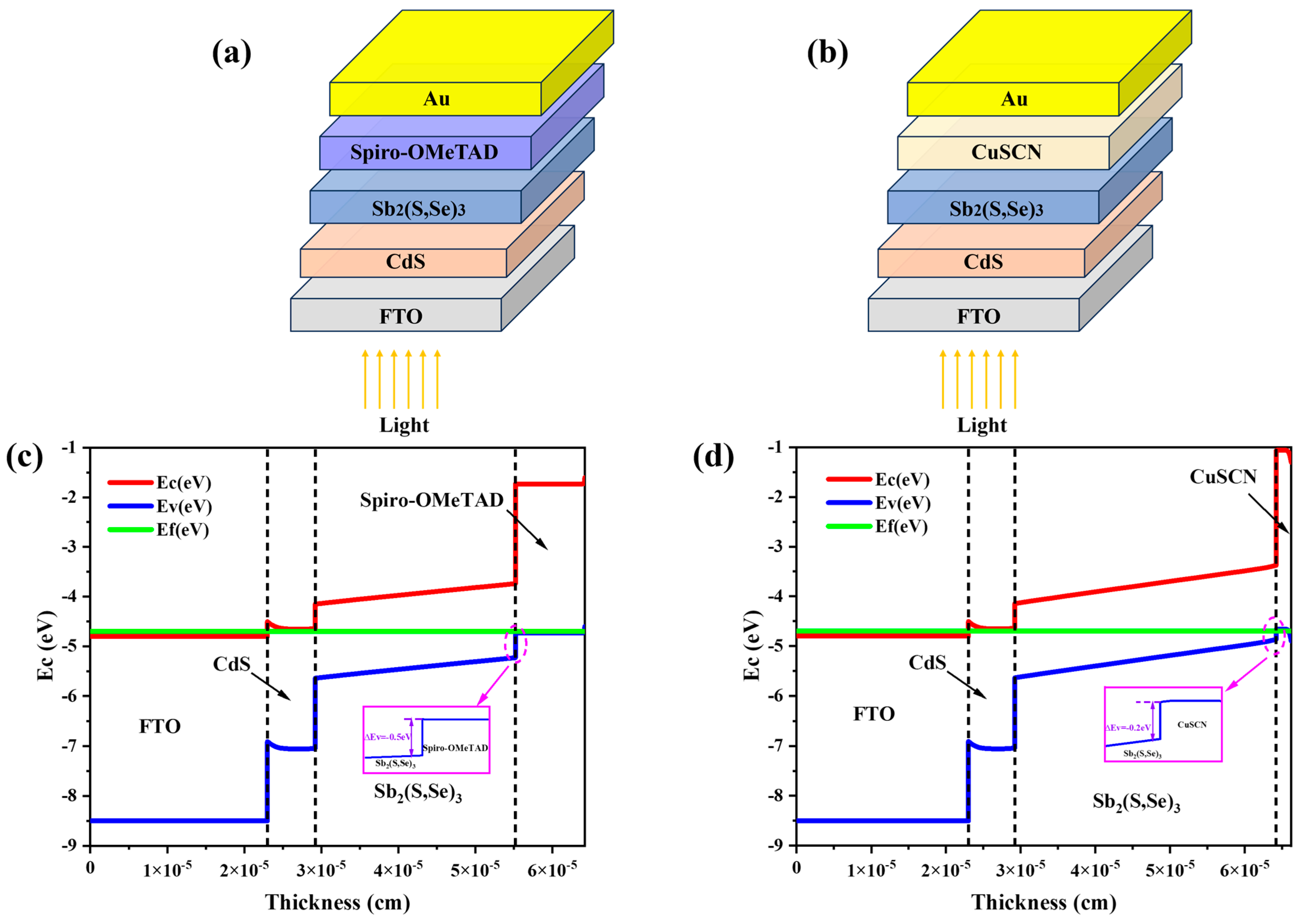
Figure 1a,b illustrate the two simulated device structures investigated in this study, specifically the conventional heterojunction using Spiro-OMeTAD as the HTL and the proposed heterojunction structure employing a CuSCN layer. Table 1 and Table 2 summarize the key parameters of these structures [35,36,37,38,39,40]. The comparative data in Table 3 show that the device using CuSCN as the HTL exhibits improvements in all photovoltaic parameters. Figure 1c,d show the energy band diagrams of Sb2(S,Se)3 solar cells with different HTLs. As shown in Figure 1c, the valence band offset (VBO) of the device with Spiro OMeTAD as the HTL is approximately 0.5 eV. In contrast, the VBO of the Sb2(S,Se)3 solar cell using CuSCN as the HTL is as low as approximately 0.2 eV (Figure 1d). This indicates that CuSCN and Sb2(S,Se)3 achieve superior band alignment. A smaller VBO directly reduces the barrier for holes at the absorber/HTL interface, thereby lowering the interface recombination velocity [38,39]. According to the thermionic emission diffusion theory, the hole current density across the interface is proportional to [40]:
J h exp ( Δ E v k T )
where ΔEv is the valence band offset. Reducing ΔEv from 0.5 eV to 0.2 eV increases the hole extraction current by more than an order of magnitude. Furthermore, the reduction in VBO suppresses the accumulation of holes at the interface, which would otherwise enhance SRH recombination via interface trap states. In addition to the valence band, the conduction band offset (CBO) also plays a role. For CuSCN, the electron affinity is 1.7 eV, creating a large conduction band spike (approximately 2.3 eV) relative to Sb2(S,Se)3 (electron affinity 4.01 eV). This large spike effectively blocks electrons from reaching the back contact, thus reducing parasitic recombination at the Au electrode. In contrast, Spiro-OMeTAD has an electron affinity of 2.0 eV, still forming a large barrier but with less favorable hole transport properties due to its lower mobility. Therefore, the combination of a reduced VBO and a strong electron blocking barrier makes CuSCN a superior HTL.
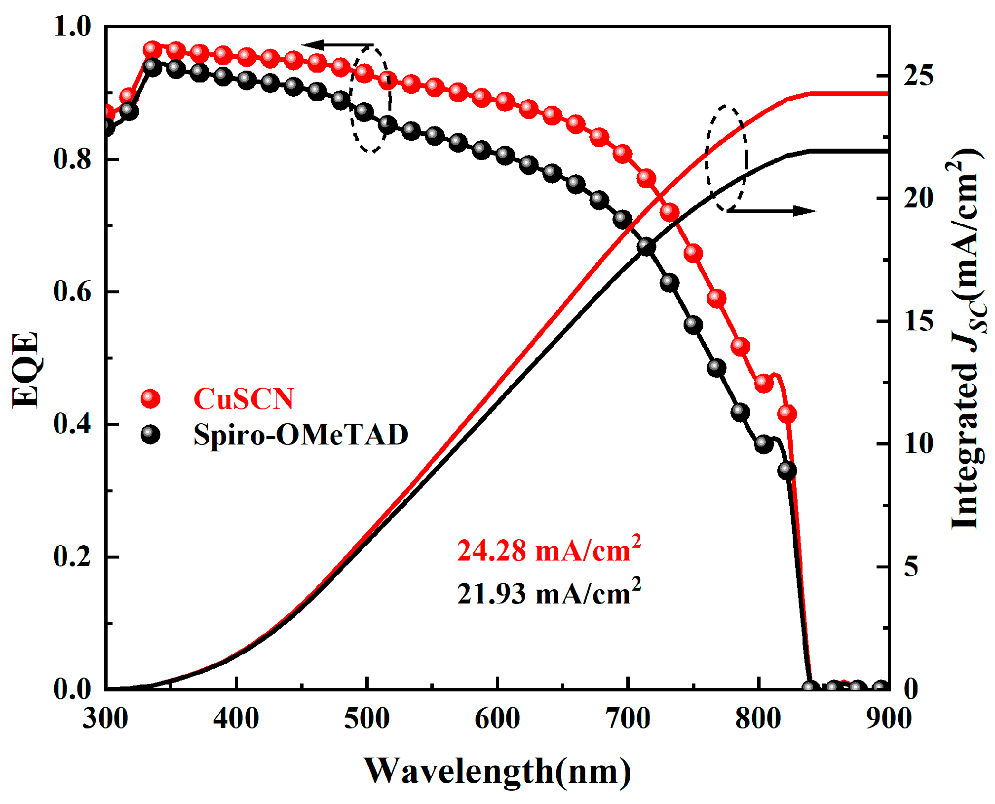
To further verify the consistency between the simulated J-V characteristics and the spectral response, we calculated the external quantum efficiency (EQE) of both devices. Figure 2 shows the simulated spectral response (SR) of the Sb2(S,Se)3 solar cells using CuSCN and Spiro-OMeTAD as HTLs. Over the entire wavelength range from 300 nm to 900 nm, the CuSCN-based device exhibits a higher SR, especially between 450 nm and 750 nm, which is the main absorption region of Sb2(S,Se)3. The integrated JSC from the SR of the CuSCN device is 22.96 mA/cm2, which is in excellent agreement with the J-V result (22.98 mA/cm2 in Table 3). For the Spiro-OMeTAD device, the integrated JSC is 20.75 mA/cm2, also consistent with its J-V value (20.78 mA/cm2). This good match confirms the reliability of our simulation model. The higher SR of the CuSCN device is attributed to the reduced valence band offset (0.2 eV) and suppressed interface recombination, as discussed in Figure 1c,d. These results further support that CuSCN is a superior HTL for high-performance Sb2(S,Se)3 solar cells.

3.2. Tuning CuSCN Parameters and Exploring Underlying Mechanisms

3.2.1. Dependence of Device Performance on Absorber Layer Thickness

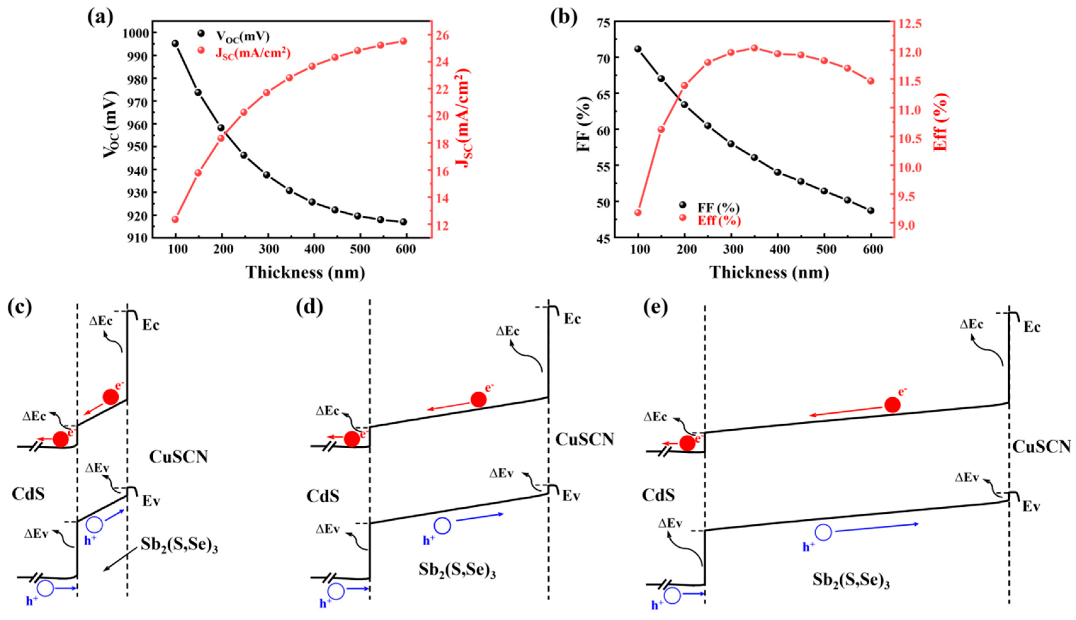
To determine the optimal balance between light absorption and charge collection, the influence of the Sb2(S,Se)3 absorber layer thickness was first simulated over a range from 100 nm to 600 nm. As shown in Figure 3a, with increasing Sb2(S,Se)3 thickness, the open circuit voltage (VOC) gradually decreases from 995.5 mV to 920.6 mV, while the short circuit current density (JSC) continuously increases from 12.96 mA/cm2 to 25.57 mA/cm2. Figure 3b shows that the fill factor (FF) decreases from 71.11% to 48.68% with increasing Sb2(S,Se)3 thickness, a decline primarily attributed to increased series resistance from the thicker absorber layer and enhanced bulk recombination [39]. Overall, as the Sb2(S,Se)3 thickness increases from 100 nm to 350 nm, the power conversion efficiency (PCE) rises from 9.18% to 12.03%. Beyond 350 nm, the PCE continuously decreases to 11.46% with further thickness increase. To reveal the physical mechanism, we analyze the depletion region and carrier collection efficiency. The absorber layer is lightly p type (1 × 1014 cm−3), and the junction is formed with n-type CdS. The depletion region width W in the absorber is given by [40]:
W = 2 ε s ( V b i V ) q N A
where Vbi is the built-in potential. For a doping concentration of 1 × 1014 cm−3, the depletion width is on the order of several hundred nano-meters. At a thickness of 100 nm, the entire absorber is depleted, resulting in a strong electric field across the whole layer. This strong field minimizes bulk recombination but also leads to incomplete absorption of long wavelength photons because the absorption depth at the band edge is around 500 nm. As thickness increases to 350 nm, a quasi-neutral region emerges near the back side. Photo-generated carriers in this region must diffuse to the depletion edge. The diffusion length Lp for holes in Sb2(S,Se)3 is estimated as [40]:
L p = D p τ p
Based on typical mobility and lifetime values, Lp is approximately 300 nm. At 350 nm, the diffusion length is comparable to the quasi-neutral region thickness, allowing efficient collection of carriers generated near the back contact. Beyond 350 nm, the quasi-neutral region becomes thicker than the diffusion length, leading to increased recombination losses. Figure 3c–e show the energy band diagrams at different thicknesses. As thickness increases, the slope of the bands in the depletion region becomes shallower because the same built-in potential is distributed over a larger distance. The electric field magnitude decreases, which reduces the drift velocity and increases the transit time, making carriers more susceptible to trap-assisted recombination. The optimum thickness of 350 nm represents a tradeoff where the depletion region still provides sufficient field-assisted collection while the quasi-neutral region does not exceed the diffusion length.

3.2.2. Effect of CuSCN Thickness on Device Performance and Interface

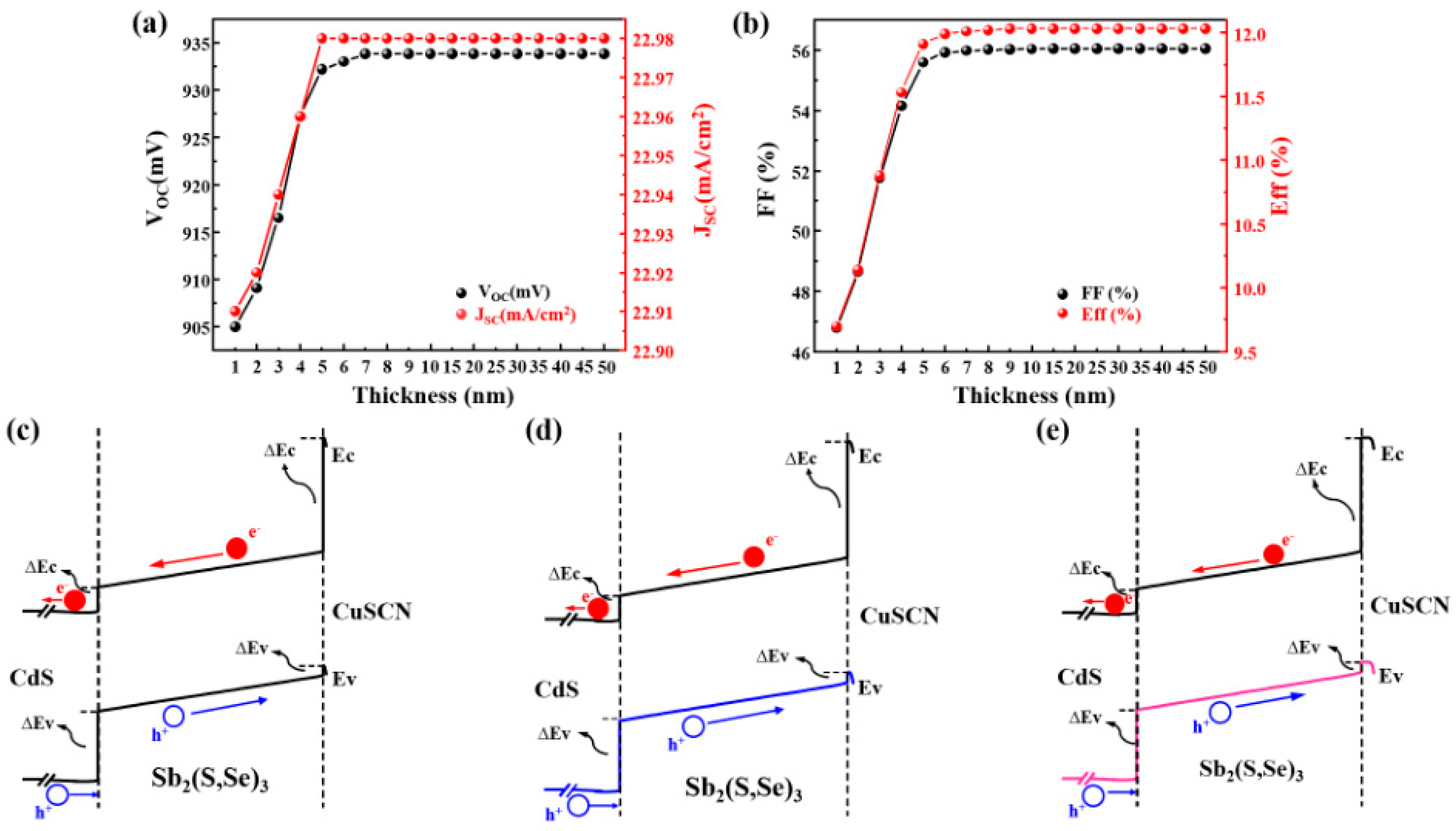
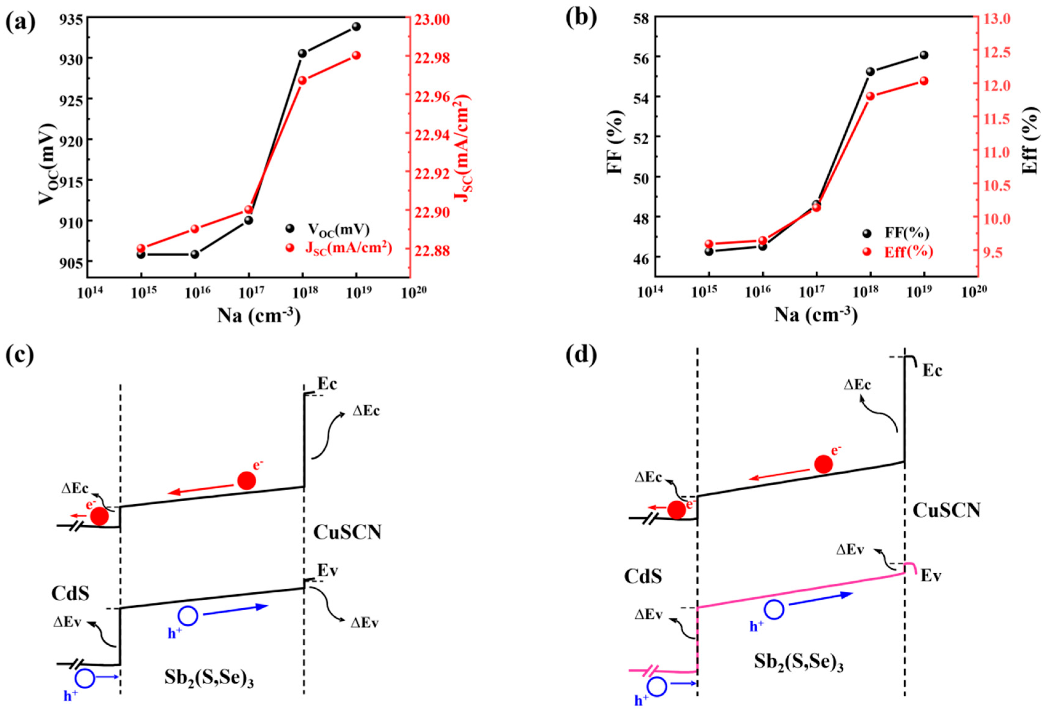
The CuSCN layer thickness (dCuSCN) critically modulates the band alignment at the Sb2(S,Se)3/CuSCN hetero-interface and the carrier transport dynamics across the back contact. Figure 4a,b present the evolution of photovoltaic parameters as dCuSCN increases from 1 nm to 20 nm. The performance exhibits a sharp rise in VOC (from 905 mV to 933.8 mV), FF (from 46.78% to 56.03%), and PCE (from 9.70% to 12.03%) as the thickness approaches 9 nm, followed by saturation beyond this value. The underlying mechanism is unequivocally identified through an analysis of the heterojunction band alignment and the thickness-dependent tunneling probability, supported by the energy band diagrams in Figure 4c–e.
For an ultrathin CuSCN layer (dCuSCN < 5 nm), the film is discontinuous, leading to direct physical contact between the Sb2(S,Se)3 absorber and the Au back electrode. The corresponding band diagram (Figure 4c) shows a sharp downward bending of the valence band at the Sb2(S,Se)3/Au interface, indicating strong Fermi-level pinning and a high density of interface trap states (Dit). This configuration forms a Schottky junction at the Sb2(S,Se)3/Au interface, characterized by a large valence band offset (ΔEv ≈ 0.5 eV). The absence of a CuSCN interlayer eliminates the electron blocking barrier, allowing photo-generated electrons to tunnel or thermionically emit into the metal. This electron leakage current increases the dark saturation current density (J0), which directly reduces the open circuit voltage through [40]:
V O C = n k T q ln ( J S C J 0 + 1 )
Furthermore, the direct metal absorber contact introduces severe Fermi-level pinning and a high density of interface trap states (Dit), which act as Shockley–Read–Hall (SRH) recombination centers. The interface recombination velocity for holes (Sp) is expressed as [40]:
S p = σ p υ t h D it
A high Sp (exceeding 105 cm/s) drastically reduces the hole extraction efficiency and degrades the fill factor. When dCuSCN increases to 9 nm, a continuous and structurally uniform CuSCN film forms. The band diagram in Figure 4d reveals a well-defined heterojunction with a minimal valence band offset of approximately 0.2 eV, creating a nearly barrier-free pathway for hole extraction. Equally important is the large conduction band offset (ΔEC ≈ 2.3 eV), which acts as a robust electron blocking layer. However, in the ultrathin regime, electrons can still tunnel through the CuSCN layer via direct tunneling. The tunneling probability (T) is exponentially dependent on thickness [40]:
T exp ( 2 d C u S C N 2 m e * Δ E c )
At dCuSCN = 5 nm, T is approximately 10−2 to 10−3, leading to measurable electron leakage. At dCuSCN = 9 nm, T decreases to below 10−6, effectively suppressing parasitic electron transport. This suppression of leakage current concurrently reduces J0 and enhances VOC. The hole transport within the CuSCN layer itself is governed by the interplay between drift and diffusion. For a heavily doped p-type CuSCN (NA = 1 × 1019 cm−3), the depletion width at the CuSCN/Au interface is given by Equation 6. With such high doping, WCuSCN is only a few nano-meters. When dCuSCN is smaller than WCuSCN, the entire CuSCN layer is fully depleted, resulting in a strong built-in electric field across the layer. Depending on the polarity of the metal work function (Au, 5.1 eV) relative to the CuSCN valence band (5.3 eV), this field can either assist or slightly impede hole flow. At 9 nm, a quasi-neutral region emerges near the metal, allowing diffusion-dominated transport with minimal resistance. The series resistance contribution from CuSCN is [40]:
R s , H T L = d C u S C N q μ p p A
For μp = 25 cm2/V·s and p = NA = 1 × 1019 cm−3, the conductivity is high. Thus, increasing dCuSCN from 9 nm to 20 nm raises Rs,HTL by only a negligible amount (on the order of 0.01 Ω·cm2), which does not affect FF. The band diagram at 20 nm (Figure 4e) is nearly identical to that at 9 nm, confirming that the electrostatic potential distribution within the HTL has stabilized. Finally, the interface recombination at the Sb2(S,Se)3/CuSCN heterojunction is minimized when the CuSCN layer is thick enough to decouple the absorber from the metal-induced gap states (MIGS) of Au. The saturation of all photovoltaic parameters for dCuSCN ≥ 9 nm, as shown in Figure 4a,b, confirms that at this critical thickness, the band alignment has stabilized, the interface trap density has reached its minimum, and the electron tunneling current has become negligible. Therefore, 9 nm is identified as the optimal CuSCN thickness, balancing complete coverage, minimal leakage, and low series resistance. Although the optimal CuSCN thickness is identified as 9 nm, depositing such a thin pinhole-free film via solution processing may be challenging. We confirm that increasing the CuSCN thickness to 30 nm or 50 nm does not degrade device performance (PCE remains ~12.0%), because all electrical benefits saturate beyond 9 nm and the additional series resistance is negligible. Hence, a thicker CuSCN layer (e.g., 30–50 nm) is recommended for experimental fabrication to ensure full coverage without sacrificing efficiency.

3.2.3. Effect of CuSCN Doping Concentration on Band Structure and Carrier Extraction

In addition to layer thickness, the doping concentration of the CuSCN HTL (NA) fundamentally determines the Fermi-level position, the depletion width at the CuSCN/Au interface, the contact resistance, and the electrostatic potential distribution within the transport layer. Figure 5a,b present the device performance as NA increases from 1015 cm−3 to 1019 cm−3. All photovoltaic parameters improve monotonically: VOC rises from 905 mV to 933.8 mV, JSC increases slightly from 22.9 to 22.98 mA/cm2, FF improves from 46.15% to 56.03%, and PCE increases from 9.56% to 12.03%. Saturation occurs at NA = 1019 cm−3. The underlying mechanisms are elucidated through doping-dependent band alignment, depletion region dynamics, and carrier transport physics, supported by the energy band diagrams in Figure 5c,d.
The CuSCN layer forms a junction with the Au back contact. For a p-type semiconductor, the depletion width WCuSCN is given by Equation (6). At a low doping concentration (NA = 1015 cm−3), WCuSCN exceeds the actual CuSCN thickness (20 nm), resulting in full depletion of the entire HTL. The corresponding band diagram (Figure 5c) reveals an upward slope of the valence band edge (Ev) from the Sb2(S,Se)3 interface toward the Au contact. This upward slope corresponds to a built-in electric field E = 1 q ( d E v d x ) that points from the metal toward the absorber. Such a field directly opposes the drift of photo-generated holes, which must travel from the absorber to the metal. The effective barrier for hole extraction is therefore increased by the potential drop across the depleted CuSCN, leading to hole accumulation at the Sb2(S,Se)3/CuSCN interface. The accumulated holes increase the local hole concentration ps at the interface, which enhances the Shockley–Read–Hall (SRH) recombination rate. The interface recombination velocity Sp is given by Equation (9). The recombination current density is [40]:
J re c = q S p ( p s p s 0 )
where ps0 is the equilibrium hole concentration. An elevated ps directly increases Jrec, raising the dark saturation current density J0. The open circuit voltage then follows Equation (8). Thus, a low NA degrades VOC through enhanced interface recombination. Moreover, the upward band slope creates a potential barrier Δ Φ = E d x that holes must overcome, effectively reducing the collection efficiency and further lowering JSC. The specific contact resistance ρc at the CuSCN/Au interface is governed by the barrier height ϕB and the doping concentration. For thermionic field emission, which dominates for moderately to heavily doped semiconductors, ρc is given by [40]:
ρ c = k q A * T exp ( 2 ε s m p * q ϕ B N A )
where A is the effective Richardson constant. At NA = 1015 cm−3, ρc is high, contributing significantly to the total series resistance Rs. As NA increases to 1019 cm−3, the exponential factor in Equation (13) decreases dramatically, making ρc negligible and the contact quasi ohmic. The series resistance contribution from the CuSCN bulk is given by Equation (11). At high doping, this term also becomes negligible.
When NA reaches 1019 cm−3, WCuSCN shrinks to only a few nano-meters, and a quasi-neutral region emerges adjacent to the metal. The band diagram in Figure 5d shows a nearly flat valence band across the entire HTL thickness. Under this flat band condition, the built-in field opposing hole transport is eliminated. Holes move by diffusion alone, and the diffusion current density is [40]:
J p = q D p d p d x q D p Δ p d C u S C N
With a high hole mobility (μp = 25 cm2/V·s) and a thin layer (20 nm), the diffusion-limited transport is highly efficient. The elimination of the parasitic field also reduces the effective series resistance, as mentioned. The flat valence band prevents hole accumulation at the Sb2(S,Se)3/CuSCN interface, reducing ps and thus Jrec from Equation (12). This suppression of interface recombination lowers J0 and further improves VOC. The saturation of all photovoltaic parameters at NA = 1019 cm−3 indicates that further doping increase does not yield additional benefits. In fact, excessively high doping (above 1019 cm−3) could introduce adverse effects such as Auger recombination, where the recombination rate scales as Cpp2n or Cnn2p, or reduced mobility due to ionized impurity scattering. However, within the simulated range, the optimal concentration is unambiguously 1019 cm−3. This value is practically achievable in CuSCN through extrinsic doping or copper vacancy engineering, providing a clear guideline for device fabrication. In addition to the band alignment and depletion effects discussed above, we also examined potential trade-offs associated with such a high doping level. At a doping concentration of 1019 cm−3, Auger recombination and ionized impurity scattering are present but do not limit device performance. The Auger lifetime (10−8 s) exceeds the SRH lifetime and carrier transit time. The hole mobility (25 cm2/V·s) already accounts for scattering losses and remains adequate for efficient transport. Doping above 1020 cm−3 would likely degrade mobility and efficiency, but this range is beyond our optimal value.

3.2.4. Effect of Operating Temperature on Device Performance

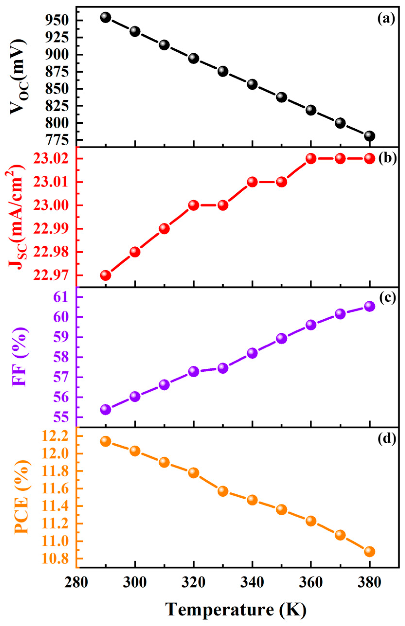
To evaluate the operational stability and thermal tolerance of the optimized Sb2(S,Se)3/CuSCN solar cell, we simulated the temperature dependence of key photovoltaic parameters over a range of 280 K to 370 K, as shown in Figure 6. As the temperature increases from 280 K to 370 K, the open-circuit voltage (VOC) decreases monotonically from 950 mV to 770 mV. This behavior is primarily attributed to the temperature dependence of the intrinsic carrier concentration (ni) and the dark saturation current (J0), following Equation (8), where J0 increases exponentially with temperature [37]. Conversely, the short-circuit current density (JSC) exhibits a very slight increase from 22.97 mA/cm2 to 23.06 mA/cm2. This minor enhancement is due to the narrowing of the bandgap (Eg) at elevated temperatures, which extends the absorption edge to longer wavelengths, albeit with a weaker effect compared to VOC. The fill factor (FF) shows a gradual improvement from 55.5% to 60.5% with rising temperature. This counter-intuitive trend can be explained by the enhanced thermal emission of trapped carriers, which effectively reduces the series resistance (Rs) and improves carrier collection efficiency in the defective absorber layer. Consequently, the power conversion efficiency (PCE) decreases from its peak of 12.02% at 280 K to 10.2% at 370 K. The decline in VOC outweighs the slight gains in JSC and FF, leading to a net negative temperature coefficient of approximately −0.055%/K. This coefficient is comparable to conventional thin-film solar cells, indicating acceptable thermal stability for practical application.

3.2.5. Influence of Absorber Bulk Defect Density on Device Performance

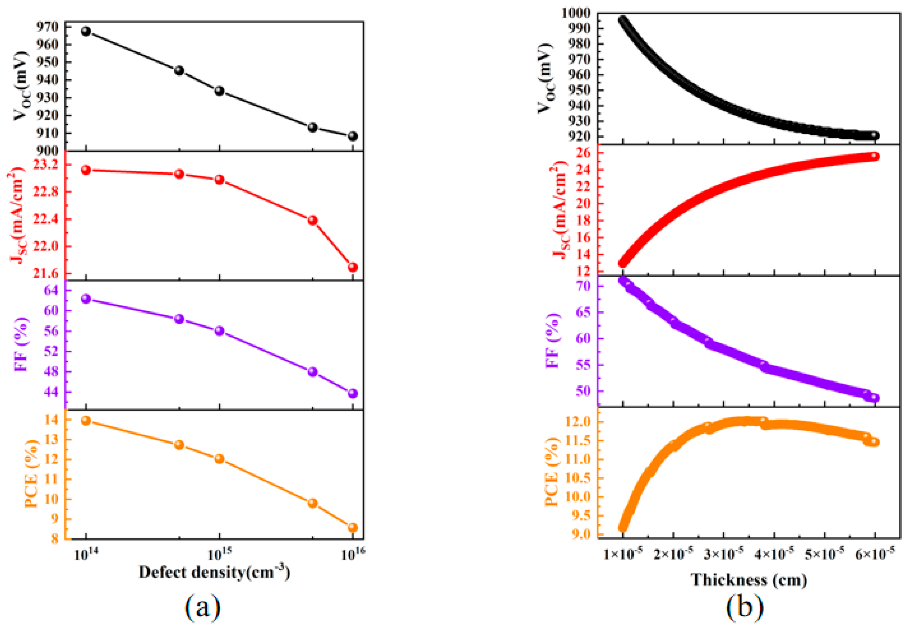
In the preceding optimization, the bulk defect density of the Sb2(S,Se)3 absorber was set to 1.3 × 1014 cm−3, representing a relatively high-quality film. To evaluate the impact of material quality, the defect density Nt was varied from 1 × 1014 cm−3 to 1 × 1016 cm−3, while keeping all other parameters at their optimized values (absorber thickness 350 nm, CuSCN thickness 9 nm, doping 1019 cm−3). The results are presented in Figure 7a. As Nt increases, the power conversion efficiency (PCE) decreases monotonically from approximately 14.0% to 10.5%. This decline is mainly caused by a reduction in open-circuit voltage (VOC) and fill factor (FF) due to enhanced Shockley–Read–Hall recombination. The short-circuit current density (JSC) shows only a slight decrease because optical generation is not directly affected by defect density.
A more practical defect density of 1 × 1015 cm−3 was then fixed, and the absorber thickness was re-scanned from 100 nm to 500 nm. The corresponding PCE values are shown in Figure 7b. The PCE increases continuously with thickness up to 500 nm, reaching about 12.0% at 500 nm, without a clear peak within this scanned range. This indicates that at this defect density, the optimal thickness is at least 500 nm, which differs from the low-defect case where the optimum was 350 nm. The discrepancy may arise from the specific defect parameters or from an incomplete thickness range (i.e., the true optimum may lie beyond 500 nm). Nevertheless, the key practical implication is that achieving high efficiency (>12%) requires the absorber defect density to be kept below approximately 1 × 1015 cm−3. For devices with poorer material quality, the expected PCE drops to 8–10%, but CuSCN still outperforms Spiro-OMeTAD under the same conditions (Table 3).

3.3. Limitations and Experimental Validation

We emphasize that this study is purely numerical. Although all input parameters are extracted from experimental literature, the simulations assume ideal interfaces, uniform defect distributions, and perfect ohmic contacts. Therefore, the predicted optimal parameters and the PCE of 12.03% should be regarded as theoretically achievable upper bounds rather than guaranteed experimental outcomes. Actual fabricated devices may exhibit lower efficiencies due to interfacial recombination, shunt paths, and process variations. Future work will focus on experimental realization of the optimized CuSCN-based Sb2(S,Se)3 solar cells to verify the simulation results.

4. Conclusions

Using AFORS HET simulations, we systematically optimized Sb2(S,Se)3 solar cells with CuSCN as the hole transport layer. CuSCN exhibits a superior valence band offset of only 0.2 eV relative to the absorber, outperforming Spiro-OMeTAD by reducing the hole injection barrier and suppressing interface recombination. An optimal absorber thickness of 350 nm balances light absorption and carrier collection, matching the depletion width with the diffusion length. A CuSCN thickness of 9 nm ensures continuous film formation, eliminates electron tunneling leakage, and adds negligible series resistance. Increasing the p-type doping concentration to 1019 cm−3 flattens the CuSCN valence band, removes the opposing built-in field, and enables diffusion-dominated hole transport. These optimizations yield a peak PCE of 12.03%. CuSCN is therefore a low-cost, stable inorganic HTL, providing a theoretical basis for high-efficiency Sb2(S,Se)3 solar cells. Long-term stability simulations or experimental validation of CuSCN under specific environmental conditions (humidity, oxygen, UV) are planned for future work.

Author Contributions

X.Z. conceptualized this study. X.Z. did simulated work. M.I. helped in data analysis. X.Z. and M.I. verified the simulation work, and revised. X.Z. wrote the initial draft, and all the authors commented on the manuscript to finalize the draft. All authors have read and agreed to the published version of the manuscript.

Funding

This research was funded by 2025 Guangdong Provincial Characteristic and Innovative Project grant number (2025KTSCX375) And The APC was funded by 2025 Guangdong Provincial Characteristic and Innovative Project.

Data Availability Statement

The original contributions presented in this study are included in the article. Further inquiries can be directed to the corresponding author.

Acknowledgments

The research is supported by the AFORS-HET (v2.5) software.

Conflicts of Interest

The authors declare no conflict of interest.

References

  1. Kannan, N.; Vakeesan, D. Solar energy for future world:—A review. Renew. Sustain. Energy Rev. 2016, 62, 1092–1105. [Google Scholar] [CrossRef]
  2. Lotfy, L.A.; Abdelfatah, M.; Sharshir, S.W.; El-Naggar, A.A.; Ismail, W.; El-Shaer, A. Numerical simulation and optimization of FTO/TiO2/CZTS/CuO/Au solar cell using SCAPS-1D. Sci. Rep. 2025, 15, 28022. [Google Scholar] [CrossRef] [PubMed]
  3. Basyouni, O.H.; Abdelfatah, M.; El-Khouly, M.E.; Mohamed, T.; El-Shaer, A.; Ismail, W. Facile and environmentally friendly fabrication of few-layer bismuthene by electrochemical exfoliation method for ultrafast photonic applications. J. Alloys Compd. 2021, 882, 160766. [Google Scholar] [CrossRef]
  4. El-Shaer, A.; Abdelfatah, M.; Basuni, A.; Mosaad, M. Effect of KOH molarity and annealing temperature on ZnO nanostructure properties. Chin. J. Phys. 2018, 56, 1001–1009. [Google Scholar] [CrossRef]
  5. Sowayan, A.; Ataya, S.; El-Naggar, A.A.; Lotfy, L.A.; Eid, A.M.; Ismail, M.; Nasser, M.; Djuansjah, J.; Abdelfatah, M.; Sharshir, S.W.; et al. Computational simulation and designing of highly efficient chalcogenide BaZrS3-based perovskite solar cells utilizing hole and electron transport materials using SCAPS. J. Phys. Chem. Solids 2025, 207, 112956. [Google Scholar] [CrossRef]
  6. El-Naggar, A.A.; Eid, A.M.; Rafat, Y.; Khamis, M.A.; Bakry, M.; Elkun, S.; Ismail, W.; Sharshir, S.W.; El-Shaer, A.; Abdelfatah, M. SCAPS simulation and design of highly efficient CuBi2O4-based thin-film solar cells (TFSCs) with hole and electron transport layers. Sci. Rep. 2025, 15, 28300. [Google Scholar] [CrossRef] [PubMed]
  7. Parida, B.; Iniyan, S.; Goic, R. A review of solar photovoltaic technologies. Renew. Sustain. Energy Rev. 2011, 15, 1625–1636. [Google Scholar] [CrossRef]
  8. Pan, Z.; Rao, H.; Mora-Seró, I.; Bisquert, J.; Zhong, X. Quantum dot-sensitized solar cells. Chem. Soc. Rev. 2018, 47, 7659–7702. [Google Scholar] [CrossRef] [PubMed]
  9. Cheng, M.; Duan, Y.; Zhang, D.; Xie, Z.; Li, H.; Cao, Q.; Qiu, Z.; Chen, Y.; Peng, Q. Tailoring Buried Interface and Minimizing Energy Loss Enable Efficient Narrow and Wide Bandgap Inverted Perovskite Solar Cells by Aluminum Glycinate Based Organometallic Molecule. Adv. Mater. 2025, 37, 2419413. [Google Scholar] [CrossRef] [PubMed]
  10. Ma, X.; Yao, X.; Zhao, Y.; Zhu, G.; Zhong, H. Life cycle toxicity and reduction potential analysis of perovskite photovoltaic technology. J. Environ. Manag. 2025, 393, 127170. [Google Scholar] [CrossRef] [PubMed]
  11. Miah Md, H.; Rahman Md, B.; Nur-E-Alam, M.; Islam, M.A.; Shahinuzzaman, M.; Rahman, R.; Ullah, H.; Khandaker, M.U. Key degradation mechanisms of perovskite solar cells and strategies for enhanced stability: Issues and prospects. RSC Adv. 2025, 15, 628–654. [Google Scholar] [CrossRef] [PubMed]
  12. Dong, J.; Gao, Q.; Wu, L.; Yang, J.; Liu, H.; Wang, W.; Tang, R.; Li, J.; Cao, Z.; Liu, Y.; et al. Carrier management through electrode and electron-selective layer engineering for 10.70% efficiency antimony selenosulfide solar cells. Nat. Energy 2025, 10, 857–868. [Google Scholar] [CrossRef]
  13. Chen, X.; Che, B.; Zhao, Y.; Wang, S.; Li, H.; Gong, J.; Chen, G.; Chen, T.; Xiao, X.; Li, J. Solvent-Assisted Hydrothermal Deposition Approach for Highly-Efficient Sb2(S,Se)3 Thin-Film Solar Cells. Adv. Energy Mater. 2023, 13, 2300391. [Google Scholar] [CrossRef]
  14. Chen, J.; Xu, C.; Li, G.; Xu, Z.; Wang, Y.; Zhang, Y.; Chen, C.; Wang, M.; He, L.; Xu, J. Se-Elemental Concentration Gradient Regulation for Efficient Sb2(S,Se)3 Solar Cells with High Open-Circuit Voltages. Angew. Chem. Int. Ed. 2024, 63, e202409609. [Google Scholar] [CrossRef] [PubMed]
  15. Dai, G.; Wang, X.; Chen, S.; Chen, X.; Che, B.; Chen, T.; Hu, P.; Li, J. Selenium-Rich Sb2(S,Se)3 Thin Films Deposited via Sequential Chemical Bath Deposition for High-Efficiency Solar Cells. Adv. Funct. Mater. 2025, 35, 2415215. [Google Scholar] [CrossRef]
  16. Shockley, W.; Queisser, H.J. Detailed Balance Limit of Efficiency of p-n Junction Solar Cells. J. Appl. Phys. 1961, 32, 510–519. [Google Scholar] [CrossRef]
  17. Rühle, S. Tabulated values of the Shockley–Queisser limit for single junction solar cells. Sol. Energy 2016, 130, 139–147. [Google Scholar] [CrossRef]
  18. Shi, X.; Zhang, F.; Dai, S.; Zeng, P.; Qu, J.; Song, J. Nanorod-textured Sb2(S,Se)3 bilayer with enhanced light harvesting and accelerated charge extraction for high-efficiency Sb2(S,Se)3 solar cells. Chem. Eng. J. 2022, 437, 135341. [Google Scholar] [CrossRef]
  19. Zhang, L.; Zheng, J.; Liu, C.; Xie, Y.; Lu, H.; Luo, Q.; Liu, Y.; Yang, H.; Shen, K.; Mai, Y. Over 10% Efficient Sb2(S,Se)3 Solar Cells Enabled by CsI-Doping Strategy. Small 2024, 20, 2310418. [Google Scholar] [CrossRef] [PubMed]
  20. Cao, R.; Lv, K.; Shi, C.; Wang, Y.; Ye, C.; Guo, F.; Hu, G.; Chen, W. Efficient Sb2S3 and Low Se Content Sb2SeyS3−y Indoor Photovoltaics. ACS Appl. Mater. Interfaces 2024, 16, 42513–42521. [Google Scholar] [CrossRef] [PubMed]
  21. Liu, D.; Zhang, W.; Pan, J.; Chen, X.; Jin, Z.; Hu, Y.; Zhang, H.; Wang, X.; Li, J. Simulation- and Experiment-Guided Design of Hole Transport Layers for Stable and Efficient All-Inorganic Sb2(S,Se)3 Solar Cells. ACS Appl. Energy Mater. 2026, 9, 530–541. [Google Scholar] [CrossRef]
  22. Xing, Y.; Guo, H.; Liu, J.; Zhang, S.; Qiu, J.; Yuan, N.; Ding, J. High-efficiency Sb2(S,Se)3 solar cells with MoO3 as a hole-transport layer. J. Alloys Compd. 2022, 927, 166842. [Google Scholar] [CrossRef]
  23. Wijeyasinghe, N.; Anthopoulos, T.D. Copper(I) thiocyanate (CuSCN) as a hole-transport material for large-area optoelectronics. Semicond. Sci. Technol. 2015, 30, 104002. [Google Scholar] [CrossRef]
  24. Zhao, K.; Munir, R.; Yan, B.; Yang, Y.; Kim, T.; Amassian, A. Solution-processed inorganic copper(I) thiocyanate (CuSCN) hole transporting layers for efficient p–i–n perovskite solar cells. J. Mater. Chem. A 2015, 3, 20544–20559. [Google Scholar] [CrossRef]
  25. Zimmermann, I.; Harada, N.; Guillemot, T.; Aider, C.; Salim, K.M.M.; Nguyen, V.S.; Castillon, J.; Provost, M.; Medjoubi, K.; Cacovich, S.; et al. Slot-Die Deposition of CuSCN Using Asymmetric Alkyl Sulfides as Cosolvent for Low-Cost and Fully Scalable Perovskite Solar Cell Fabrication. Sol. RRL 2024, 8, 202400064. [Google Scholar] [CrossRef]
  26. Baranwal, A.K.; Kanda, H.; Shibayama, N.; Ito, S. Fabrication of fully non-vacuum processed perovskite solar cells using an inorganic CuSCN hole-transporting material and carbon-back contact. Sustain. Energy Fuels 2018, 2, 2778–2787. [Google Scholar] [CrossRef]
  27. Niu, H.; Xiao, C.; Xu, J.; Xie, C.; Duan, M.; Bu, Z.; Li, W. Solvent-Induced Copper Vacancy in CuSCN Layer: A Strategy to Boost Conductivity and Optimize Energy Levels for Efficient Organic Solar Cells. Adv. Funct. Mater. 2025, 35, 2413167. [Google Scholar] [CrossRef]
  28. Froitzheim, A.; Stangl, R.; Elstner, L.; Kriegel, M.; Fuhs, W. AFORS-HET: A computer-program for the simulation of heterojunction solar cells to be distributed for public use. In Proceedings of the 3rd World Conference on Photovoltaic Energy Conversion; IEEE: New York, NY, USA, 2003; Volume 1, pp. 279–282. [Google Scholar]
  29. Stangl, R.; Leendertz, C.; Haschke, J. Numerical Simulation of Solar Cells and Solar Cell Characterization Methods: The Open-Source on Demand Program AFORS-HET. In Solar Energy; IntechOpen: London, UK, 2010. [Google Scholar] [CrossRef] [PubMed]
  30. Nicolás-Marín, M.M.; Ayala-Mato, F.; Vigil-Galán, O.; Courel, M. Simulation analysis of Cd1−xZnxS/Sb2(Se1−xSx)3 solar cells with n-i-p structure. Sol. Energy 2021, 224, 245–252. [Google Scholar] [CrossRef]
  31. Sharma, A.; Yadav, E.; Himanshu; Dhaka, M.S. Exploration of All-Inorganic Pb-Free CsSnI3-Based Perovskite Solar Cells: Performance Optimization by SCAPS-1D Simulation Approach. Phys. Status Solidi (a) 2025, 223, e202500692. [Google Scholar] [CrossRef]
  32. Barthwal, S.; Singh, S.; Chauhan, A.K.; Karuppannan, R. Design and Simulation of CdS-Free Sb2(S,Se)3 Solar Cells with Efficiency Exceeding 20%. ACS Sustain. Chem. Eng. 2024, 12, 947–958. [Google Scholar] [CrossRef]
  33. Huang, L.; Sun, X.; Li, C.; Xu, R.; Xu, J.; Du, Y.; Wu, Y.; Ni, J.; Cai, H.; Li, J.; et al. Electron transport layer-free planar perovskite solar cells: Further performance enhancement perspective from device simulation. Sol. Energy Mater. Sol. Cells 2016, 157, 1038–1047. [Google Scholar] [CrossRef]
  34. Dabbabi, S.; Nasr, T.B.; Kamoun-Turki, N. Parameters optimization of CIGS solar cell using 2D physical modeling. Results Phys. 2017, 7, 4020–4024. [Google Scholar] [CrossRef]
  35. Azri, F.; Meftah, A.; Sengouga, N.; Meftah, A. Electron and hole transport layers optimization by numerical simulation of a perovskite solar cell. Sol. Energy 2019, 181, 372–378. [Google Scholar] [CrossRef]
  36. Chen, H.; Bryant, D.; Troughton, J.; Kirkus, M.; Neophytou, M.; Miao, X.; Durrant, J.R.; McCulloch, I. One-Step Facile Synthesis of a Simple Hole Transport Material for Efficient Perovskite Solar Cells. Chem. Mater. 2016, 28, 2515–2518. [Google Scholar] [CrossRef]
  37. Arumugam, G.M.; Karunakaran, S.K.; Liu, C.; Zhang, C.; Guo, F.; Wu, S.; Mai, Y. Inorganic hole transport layers in inverted perovskite solar cells: A review. Nano Sel. 2021, 2, 1081–1116. [Google Scholar] [CrossRef]
  38. Saha, N.; Brunetti, G.; Carlo, A.D.; Ciminelli, C. Efficiency boost of perovskite solar cell in homojunction configuration through tailored band alignment and p–n doping profile. J. Phys. Energy 2025, 7, 045009. [Google Scholar] [CrossRef]
  39. Meyer, E.L.; Mvokwe, S.A.; Oyedeji, O.O.; Rono, N.; Agoro, M.A. Computational Study of Chalcogenide-Based Perovskite Solar Cell Using SCAPS-1D Numerical Simulator. Materials 2025, 18, 186. [Google Scholar] [CrossRef] [PubMed]
  40. Abbas, S.; Bajgai, S.; Chowdhury, S.; Najm, A.S.; Jamal, M.S.; Techato, K.; Channumsin, S.; Sreesawet, S.; Channumsin, M.; Laref, A.; et al. Numerical Simulation of the Performance of Sb2Se3 Solar Cell via Optimizing the Optoelectronic Properties Based SCAPS-1D. Materials 2022, 15, 6272. [Google Scholar] [CrossRef] [PubMed]
Figure 1. (a) Model diagram of a Sb2(S,Se)3 device with Spiro-OMeTAD as the HTL, (b) model diagram of a Sb2(S,Se)3 device with CuSCN as the HTL, (c) band diagram of a Sb2(S,Se)3 device with Spiro-OMeTAD as the HTL, (d) band diagram of a Sb2(S,Se)3 device with CuSCN as the HTL. (The dotted lines are used to distinguish each layer of the device).
Energies 19 03088 g001
Figure 2. Simulated external quantum efficiency (EQE) spectra of Sb2(S,Se)3 solar cells using CuSCN and Spiro-OMeTAD as hole transport layers. The integrated JSC values are 22.96 mA/cm2 (CuSCN) and 20.75 mA/cm2 (Spiro-OMeTAD), which are consistent with the J-V results in Table 3.
Energies 19 03088 g002
Figure 3. Relationship between the thickness of Sb2(S,Se)3 and (a) VOC and JSC, and (b) FF and PCE; band diagrams for Sb2(S,Se)3 layers with thicknesses of (c) 100 nm, (d) 350 nm, and (e) 600 nm.
Energies 19 03088 g003
Figure 4. Relationship between the thickness of CuSCN and (a) VOC and JSC, and (b) FF and PCE; band diagrams for CuSCN layers with thicknesses of (c) 1 nm, (d) 9 nm, and (e) 50 nm.
Energies 19 03088 g004
Figure 5. Relationship between the doping concentration of CuSCN and (a) VOC and JSC, and (b) FF and PCE; energy band diagrams corresponding to CuSCN doping concentrations of (c) 1015 cm−3 and (d) 1019 cm−3.
Energies 19 03088 g005
Figure 6. Relationship between the temperature and (a) VOC, (b) JSC, (c) FF and (d) PCE of solar cells.
Energies 19 03088 g006
Figure 7. (a) PCE of the Sb2(S,Se)3 solar cell as a function of bulk defect density in the absorber layer. Other parameters are fixed at their optimal values (absorber thickness 350 nm, CuSCN thickness 9 nm, doping 1019 cm−3), and (b) PCE as a function of absorber thickness at a fixed bulk defect density of 1 × 1015 cm−3. Other parameters are the same as in (a).
Energies 19 03088 g007
Table 1. Material parameters of each layer used in numerical simulations.
ParametersFTOCdSSb2(S,Se)3Spiro-OMeTADCuSCN
Thickness (nm)230623509020
εr91014.38310
χ (eV)4.84.54.0121.7
Eg (eV)3.72.41.4933.6
NC (cm−3)2.2 × 10182.2 × 10182.2 × 10182.5 × 10182.2 × 1019
NV (cm−3)1.8 × 10191.8 × 10191.8 × 10201.8 × 10191.8 × 1018
µe [cm2/Vs]20100141.0 × 10−4100
µp [cm2/Vs]10252.62.0 × 10−425
NA (cm−3)1.0 × 10145.0 × 10181.0 × 1019
ND (cm−3)1.0 × 10204.0 × 1017
v t h e [cm/s]1.0 × 1071.0 × 1071.0 × 1071.0 × 10181.0 × 107
v t h p [cm/s]1.0 × 1071.0 × 1071.0 × 1071.0 × 10181.0 × 107
Table 2. Bulk defect parameters of materials used in numerical simulations.
Defect ParametersFTOCdSSb2(S,Se)3Spiro-OMeTADCuSCN
Defect 1Defect 2
TypeSingle
acceptor
Single
donor
Single
acceptor
Single
acceptor
Single
acceptor
Single
donor
Nt (cm−3)1.0 × 10151.0 × 10141.3 × 10141.0 × 10151.0 × 10181.0 × 1015
σe (cm2)1.0 × 10−153.0 × 10−151.99 × 10−141.99 × 10−141.0 × 10−151.0 × 10⁻¹⁵
σh (cm2)1.0 × 10−152.0 × 10−141.99 × 10−141.99 × 10−141.0 × 10−151.0 × 10⁻¹⁵
Table 3. Photovoltaic performance of Sb2(S,Se)3 thin-film solar cells with different hole transport layers.
ParametersVOC (mV)JSC (mA/cm2)FF (%)PCE (%)Rs (Ω·cm2)Rsh (Ω·cm2)
Spiro-OMeTAD904.220.7844.278.315551500
CuSCN933.822.9856.0312.03322000
Disclaimer/Publisher’s Note: The statements, opinions and data contained in all publications are solely those of the individual author(s) and contributor(s) and not of MDPI and/or the editor(s). MDPI and/or the editor(s) disclaim responsibility for any injury to people or property resulting from any ideas, methods, instructions or products referred to in the content.