Article

Electrode Erosion and Prefire Studies Towards Fusion Scale Pulsed Power

by
Luke Boswell
1,*,
Raimi Clark
1,
Jacob Stephens
1,
John Mankowski
1,
James Dickens
1,
Adam Steiner
2,
Max Flynn
2 and
Andreas Neuber
1,*
1
Center for Pulsed Power and Power Electronics, Texas Tech University, Lubbock, TX 79409, USA
2
Sandia National Laboratories, Albuquerque, NM 87115, USA
*
Authors to whom correspondence should be addressed.
Energies 2026, 19(13), 3043; https://doi.org/10.3390/en19133043
Submission received: 21 May 2026 / Revised: 23 June 2026 / Accepted: 25 June 2026 / Published: 27 June 2026

Abstract

This study presents a comprehensive investigation of electrode erosion and discharge behavior in spark gap switches over long switching cycle lifetimes. Brass, copper–tungsten (CuW), and stainless steel electrodes are tested under controlled conditions to quantify material degradation, debris accumulation, and changes in breakdown voltage. High-resolution imaging and statistical analysis of spark channel locations and gap breakdown voltages reveal how surface evolution influences long-term performance and reliability. These results provide essential data for lifetime modeling and inform design strategies for pulsed power systems in emerging applications such as private sector fusion energy and large-scale facilities like Sandia’s Z Machine and proposed ZX upgrades, where high repetition reliability and predictable behavior are critical.

1. Introduction

Spark gap switches are widely used in pulsed power systems for their ability to handle extreme electrical stress in voltage, current, and operating time, with minimal inductance. While their fundamental operation is well understood, long-term reliability under extended cycling poses a significant challenge. Electrode erosion, debris deposition, and evolving surface morphology can significantly alter breakdown characteristics over time, impacting system performance and maintenance requirements [1]. Long-lifetime considerations are particularly relevant for the growing private fusion energy sector, where pulsed power systems must deliver precise, high-energy bursts repeatedly and reliably. Concepts such as inertial confinement and magneto-inertial fusion demand switching components that can sustain tens of thousands of cycles without degradation of performance. Similarly, heightened reliability demands are prevalent not only in the switches, but across the entirety of the next generation of pulsed power research drivers, such as the concepts which would lead to the planned ZX initiative [2,3], whose intricate setups, increased number of switches, particularly for linear transformer drivers [4], and high costs per pulse amplify the consequences of unreliability. One of the more problematic manifestations of spark gap unreliability and lifetime limitation is prefire, in which a spark gap switch closes at substantially less than its nominal operating voltage. In this work, catastrophic prefire events are considered to be those in which a switch closes at 60 percent or less of its nominal operating voltage, corresponding to the operating conditions of Sandia’s Z Machine. While the percentage of self-breakdown voltage at which a prefire can be classified as catastrophic varies with the design of any specific pulsed power machine, prefire failures can pose significant consequences for any machine. The prefire of any single component can cause the loss of a shot and its corresponding experiment, as well as component damage and destruction. The high component numbers of the largest pulsed power machines accordingly require high per-component reliability that can be difficult to assess, as extrapolation from distributions generated by low shot count research drivers under-predicts the rate of prefires. Despite this, detailed descriptions of material-specific erosion, beyond the rate of material removal, and the statistical progression of spark channel locations are scarce, limiting predictive modeling and design optimization to avoid features that may lead to prefire.
Building on these considerations, prior research has established a substantial, yet incomplete, foundation for understanding electrode erosion and long-term spark gap behavior. Foundational studies by Donaldson and colleagues provided some of the earliest systematic examinations of erosion mechanisms in high-energy spark gaps, documenting crater formation, macroscopic growths, and polarity-dependent material removal in various materials under high current, repetitively pulsed conditions. Additionally, Donaldson observes a strong dependence on the switch gas used, with complex plasma-surface interactions contributing to the realizable lifetime of the switch [1,5,6,7].
More recent work addresses switch lifetime and reliability in the context of the performance demands of modern pulsed power machines and their applications, with considerations of triggering jitter and performance at high repetition rates becoming increasingly prominent as well [8,9,10,11,12]. Simultaneously, a better understanding of foundational erosion mechanisms and predictive modeling provides an enhanced understanding of electrode lifetime. Researchers equipped with models based on heat conduction and molten pool behavior [13] are now able to demonstrate strong agreement between Monte Carlo predictions and long-duration experimental results [14,15]; however, Monte Carlo predictions are inherently unable to capture the anomalous low voltage failures sought in this work without a better understanding of the mechanism that causes them.
One finds that while the existing body of literature has thoroughly documented spark gap electrode erosion tendencies and characteristics across a variety of materials and conditions, the treatment remains incomplete. Given the broad range of types and applications of spark gap switches, there exists a broad range of spark gap lifetime experiments, and one can encounter incomplete areas in the literature by virtue of this range. For example, the meaning of long lifetime is application specific; in this work, a switch lifetime corresponds to the 10,000 shot lifetime of the widely used T-670 spark gap [16], whereas extremely high current and charge transfer applications have shorter lifetimes, such as the 2000 shot lifetime of the T-508 switch [17], and repetitive pulsed power systems can readily exceed 10,000 switching events in seconds. Similarly, one must take care not to assume the performance of one system will be applicable to another system with vastly different operating conditions. As an example, the nature of a prefire event in a fast, triggered switch operating in an E / p vs. p τ regime [18] is different from the nature of a prefire event in a DC charging environment such as the one presented in this experiment. In addition to those, spanning the entire body of literature is, perhaps, the most prominent remaining gap, which is the lack of detailed data capturing erosion and electrode surface conditions as wear and debris accumulate. Along with data on spark localization on electrode surfaces, these data are essential in the development of predictive models for spark gap switches suited for operation in stringent, high-reliability, long-lifetime applications.
To address this deficiency, this work systematically examines the lifetime behavior of three common electrode materials, brass, copper–tungsten (CuW), and stainless steel, over extended experiments. High-resolution imaging captures the evolving electrode surface conditions, debris accumulation, and spark channel distribution over the course of the electrodes’ lifetimes, with the intention of identifying any links between prefire failures and the electrode surface conditions that preceded them. These insights will guide the development of robust, spark gap switches tailored to the stringent demands of next-generation pulsed power systems for high-energy-density (HED) physics research and fusion energy applications. In addition to improved hardware, the per-discharge imagery data captured in this work stands to improve modeling efforts via the integration of substantially more granular electrode surface topology and wear information.

2. Materials and Methods

2.1. High Voltage System

In order to evaluate spark gap electrode reliability, it is critical to provide repeatable and reliable electrical excitation, as well as a suitable experimental environment. To this end, the experimental apparatus first presented in [19] has been continuously refined over the course of this work, resulting in the machine presented in this section.
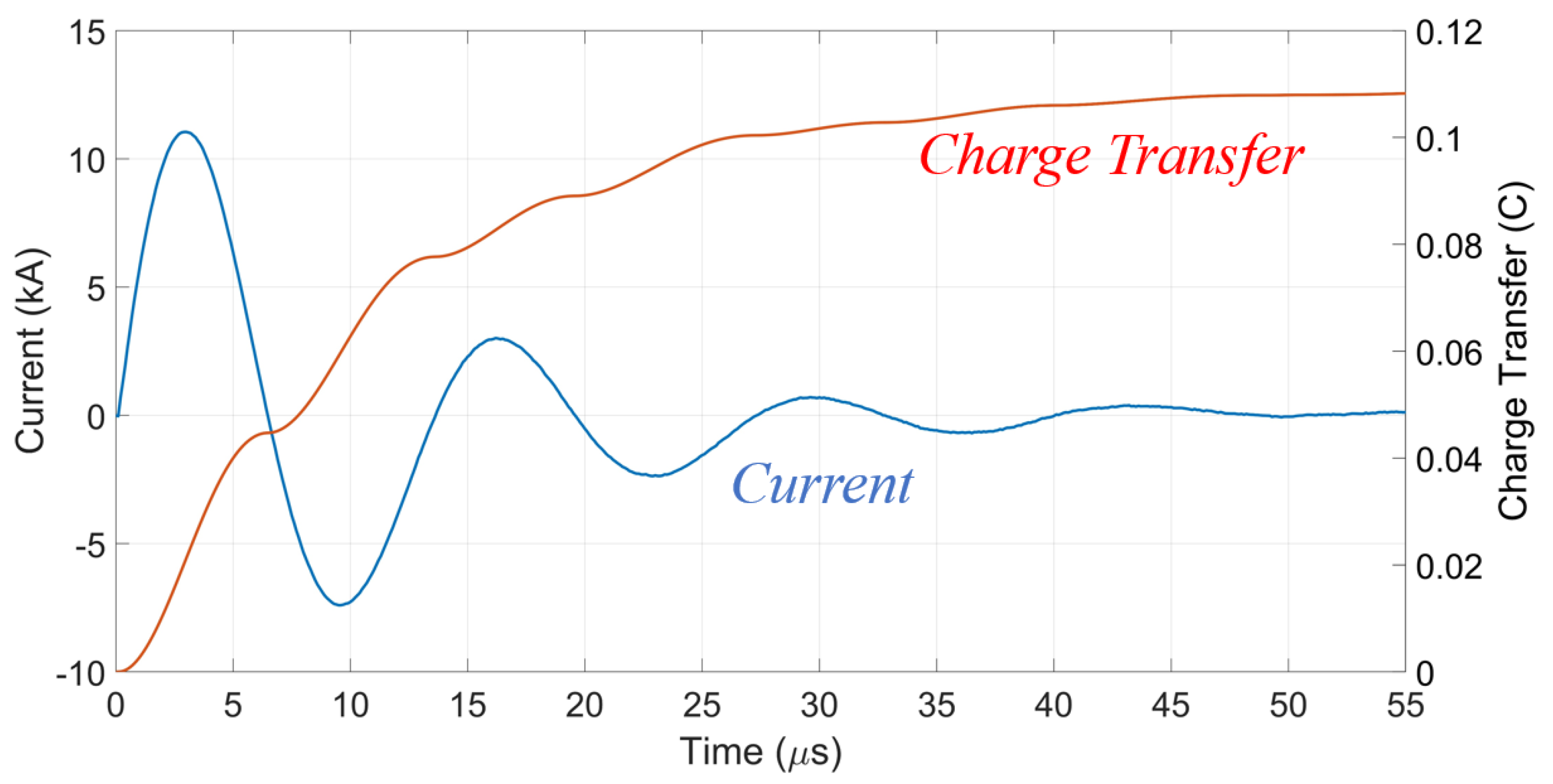
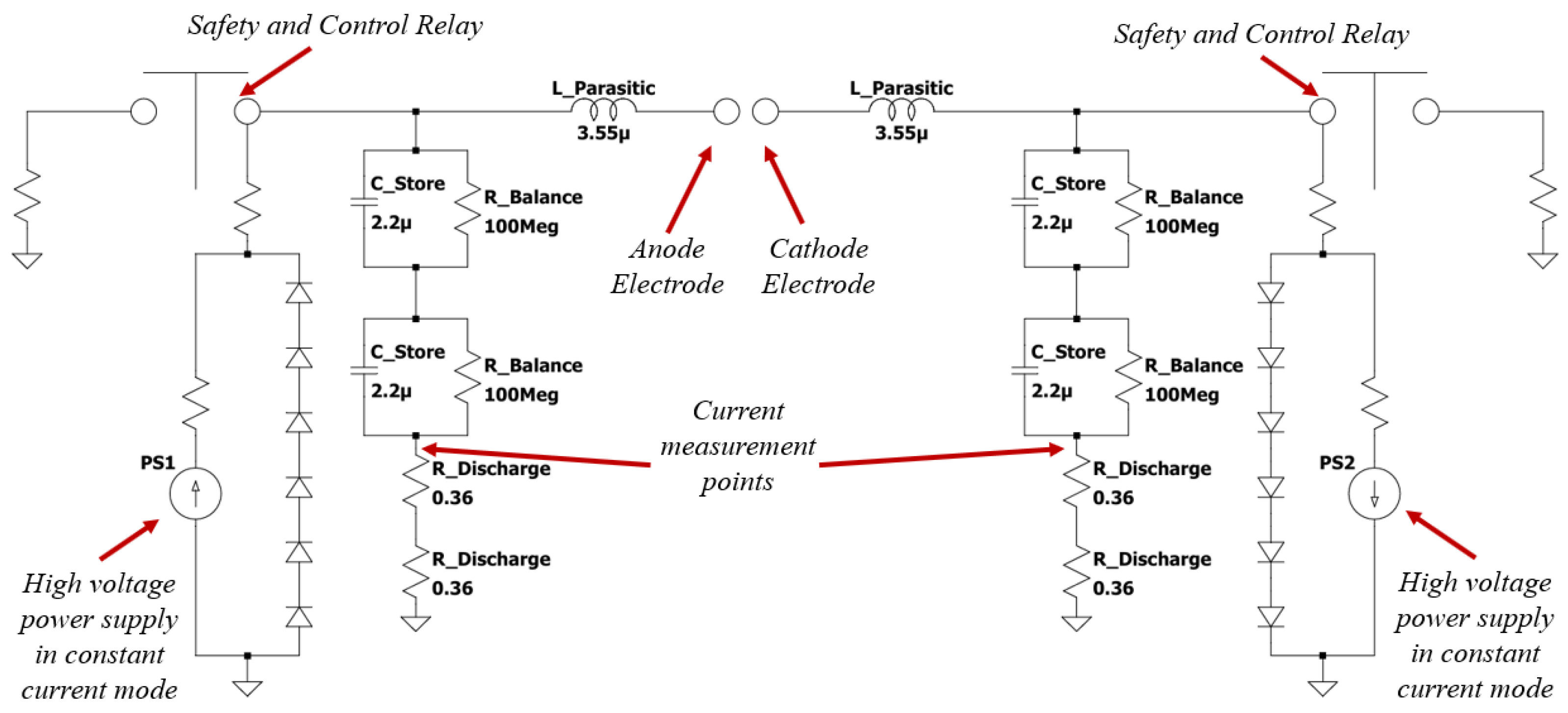
As this work is performed with the ultimate aim of understanding and diagnosing switch prefires during DC charging, no pulse shaping or conditioning considerations need to be made; switch closure results in the RLC discharge seen in Figure 1. In order to allow access to high electrical stress across the spark gap while minimizing electrical stress everywhere else, bipolar charging is used; accordingly, all high voltage components have a duplicate, as seen in Figure 2. Two 1.1 μ F capacitor banks, each constructed of two 2.2 μ F resistively balanced capacitors in series, are connected to the spark gap, one pair per polarity. They are each rated for 100 kV operation; this over-rating ensures the longevity of the capacitors, which are intended to see tens of thousands of charge-discharge cycles, by minimizing the electrical stress that they are subjected to. These capacitors are charged by high voltage power supplies delivering constant current, which results in a linear 1 kV/s voltage ramp applied to each electrode prior to breakdown. Experiments are configured with a maximum operating voltage of 90 kV differential and a maximum intended breakdown voltage of 80 kV across the gap, or lower as required for electrode performance or to meet the needs of a particular experiment; the ability to charge beyond the nominal point of breakdown ensures that a full statistical distribution of breakdown voltages is captured. The total parasitic inductance of the system is 7.1 μ H, determined by matching circuit simulations to measured current waveforms. Parasitic inter-electrode capacitance is calculated by electrostatic simulation to be less than 1.5 pF, and, owing to the slow charging operation of the spark gap, does not make a measurable impact on switch operation. When the system is charged to ±40 kV, 1760 J of energy is stored, and approximately 0.14 C of charge is transferred upon switch closure.
The experiment is fully automated: both power supplies operate under remote control and report their status to the central control system, which monitors charging for faults or abnormalities and logs the breakdown voltage. The voltage resolution of the control system is approximately 10 V. Two remotely controlled high voltage relays manage the charge-discharge sequence. When open, they allow the capacitors to charge; when closed, they divert stored energy into resistors capable of safely dissipating a full capacitor charge. The relays are closed between discharges so that each cycle begins with zero voltage across the gap, ensuring a consistent charging profile throughout the experiment, as well as negligible voltage pre-stress on the gap prior to charging.
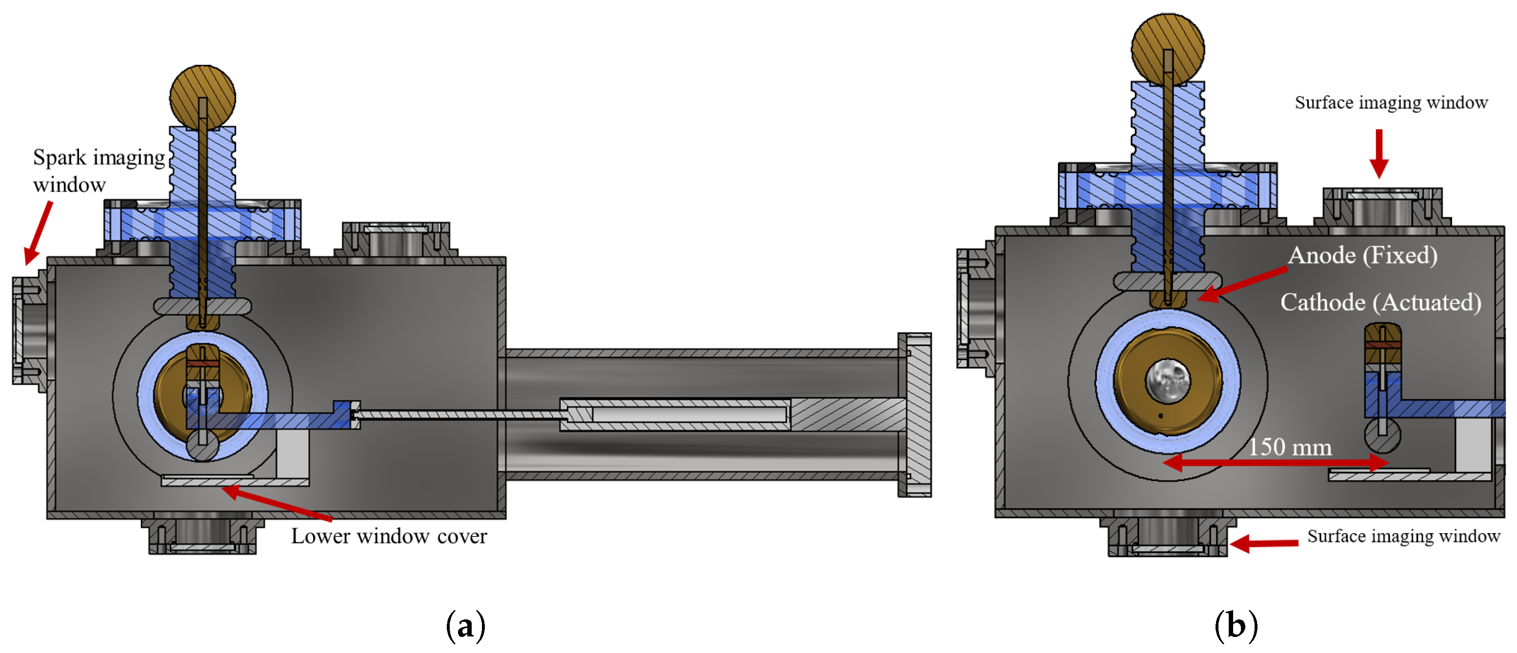
As both electrode surfaces, in addition to the plasma channel itself, are imaged, the use of a traditional spark gap body is impossible. Instead, the electrodes are located within a stainless steel pressure vessel equipped with windows to permit imaging. The gas environment within the pressure vessel is set manually via an absolute pressure gauge, with a remotely actuated valve used to exhaust gas and subsequently refill during the experiment, typically 10 s of exhausting gas every five shots, which is a compromise between maintaining a fresh gas volume during the experiment and minimizing the amount of switch gas consumption. The switch gas used in this work is supplied via 18 bottles of ultra-zero air, certified by the supplier, Linde Gas and Equipment Inc., Houston, TX, USA, as containing less than 0.1 parts per million (ppm) total hydrocarbons and less than 2 ppm water, connected in parallel via a manifold in order to ensure a reliable supply of gas to the pressure vessel. A pair of custom feedthroughs deliver high voltage into the pressure vessel. The anode electrode is connected directly to its feedthrough, while the cathode electrode is connected to a moving arm to permit the imaging described in Section 2.3; the cathode is electrically connected to its feedthrough via a flexible high voltage cable qualified for operating in a high-stress and vibration environment.

2.2. Electrodes and Materials

Experiments have been performed on three materials of interest, 304L stainless steel, 360 brass, and copper–tungsten (CuW, Plansee USA LLC, Franklin, MA, USA), whose characteristics are described in Table 1. The stainless steel and the brass are both metal alloys, but CuW is a metal matrix in which molten copper is infiltrated into sintered tungsten powder [20], as opposed to an alloy formed by melting constituent metals together. All experiments to date have been performed using Rogowski profile electrodes, which produce a uniform electric field profile to distribute the locations of successive discharges across the face of the electrodes [21,22]. As this profile is a function of electrode spacing; the exact shape of the electrode surface varies in order to match the experiment’s desired gap spacing, gas pressure, and breakdown voltage. Stainless steel and brass electrodes are 25.4 mm (1 inch) in diameter, and have a uniform field region 22.5 mm (0.9 in) in diameter; minor variations to this typical profile have also been tested, with only negligible changes in outcome. CuW electrodes are 38.1 mm (1.5 inch) in diameter, with a 35.5 (1.4 in) diameter uniform field region. Each electrode is 12.7 mm (0.5 inch) tall. Brass and stainless steel electrodes are polished prior to experimentation, whereas CuW electrodes are tested as-machined in order not to further disturb the composition of the metal matrix; all electrodes are cleaned with ethanol immediately prior to installation in the pressure vessel.

2.3. Imaging

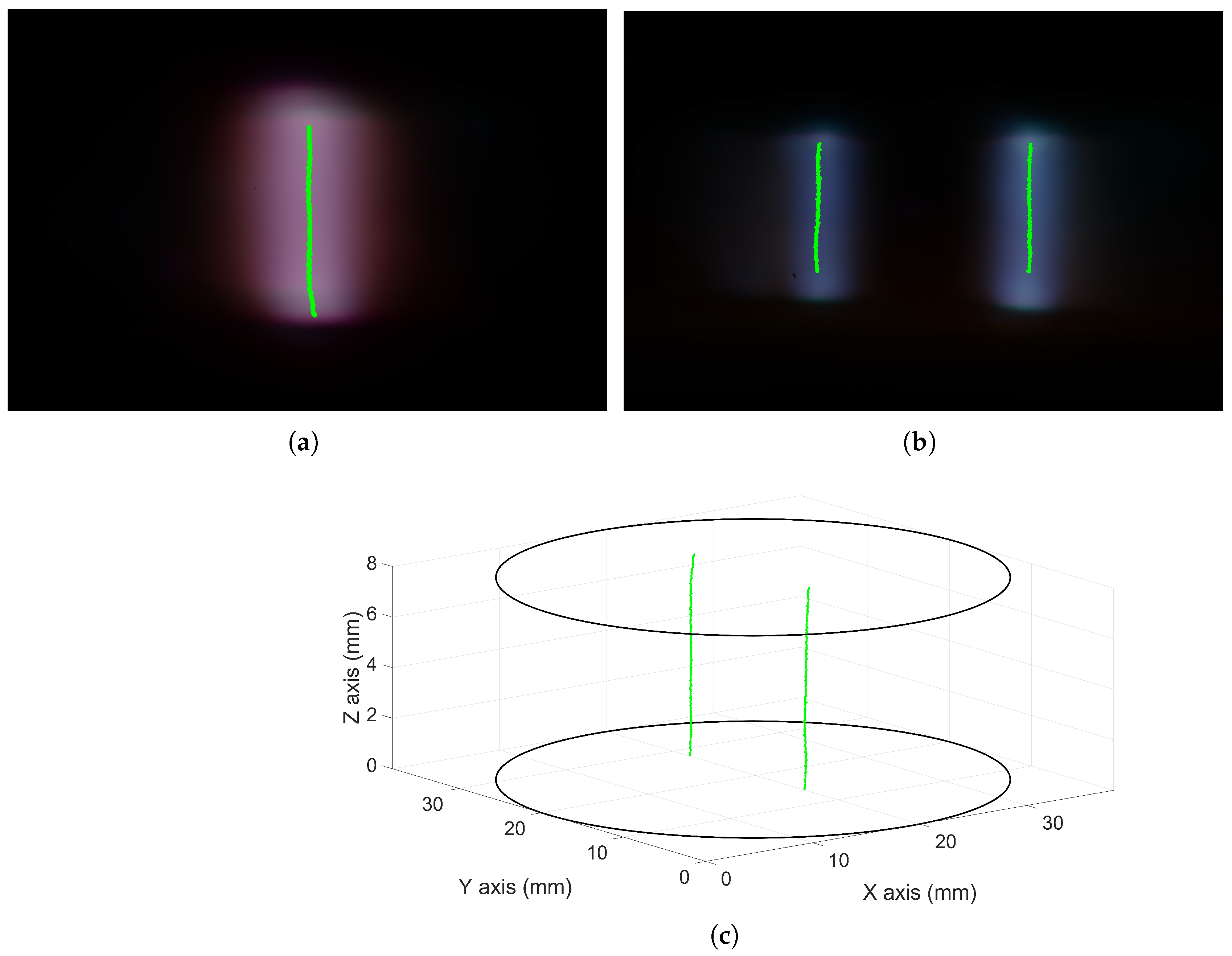
Over the course of an experiment, tens of thousands of images are captured by four Nikon D610 full-frame DSLR cameras, each equipped with a 27× zoom spotting scope and 1.4× teleconverter, which maximizes sensor utilization while keeping the cameras approximately 2.1 m (7 ft) away from the spark gap for electromagnetic interference (EMI) mitigation. Two of these cameras are equipped with variable attenuation neutral density filters, up to OD 3.3, and capture each discharge. These cameras are positioned 90 degrees apart around the spark gap, which allows their images to be used to reconstruct plasma channels in three dimensions and observe where those plasma channels interact with electrode surfaces, as in Figure 3.
The other two cameras view the pressure vessel’s upper and lower windows via mirrors and are used to image the electrode surfaces. Surface imaging is accomplished by retracting the piston that the lower electrode is mounted on, seen in Figure 4.
When the piston is retracted, the lower electrode is aligned with the pressure vessel’s upper window, while the upper electrode is simultaneously revealed through the lower window. Lighting within the pressure vessel is synchronized to the camera shutters in order to provide consistent illumination for each surface image. After surface imaging is complete, the piston is extended, and the two electrodes align vertically as a spark gap again, and charging begins for the next cycle; the volume of pictures captured over the course of an experiment confirms the consistent placement of the moving electrode shot to shot, as an inconsistency in position would manifest as unusable post-processed surface image data. Knowing the resolution of the surface cameras to be approximately 230 pixels per millimeter, and asserting that a ten-pixel offset would be able to create substantial artifacts in post-processed data, the lack of such artifacts implies that the cycle-to-cycle change in position is less than approximately 45 μ m. These imaging capabilities allow for as close to in-situ imagery as possible, and ensure that the electrode surface conditions are captured before any abnormally low voltage switch closures.
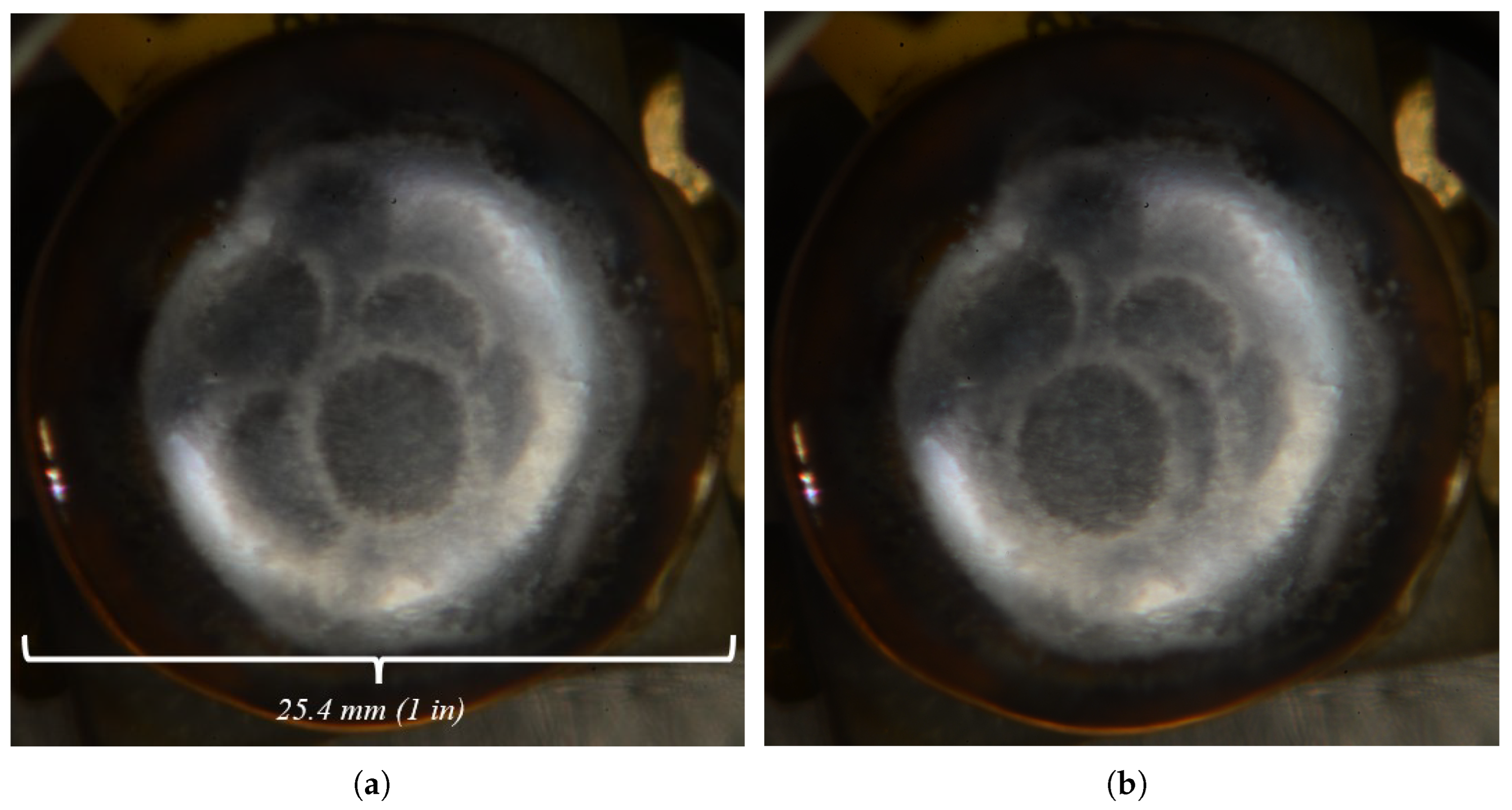
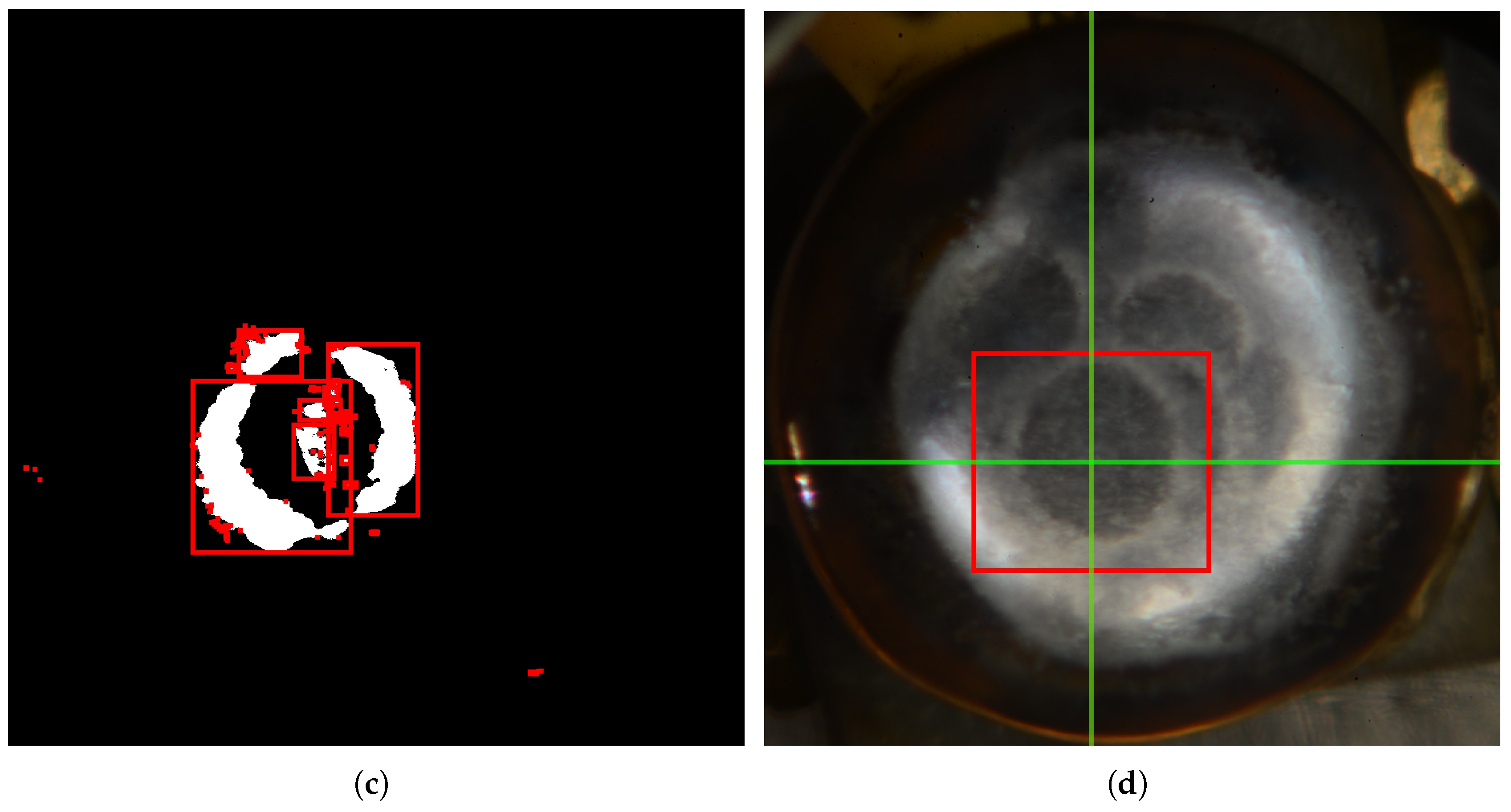
Post-experiment analysis of electrode surface images provides complementary capabilities to the analysis of spark images. Notably, both spark and surface image methods can locate a plasma channel on an electrode’s surface. Surface image analysis, the methodology of which is depicted by Figure 5, is unable to distinguish between damage craters from multiple plasma channels and large debris accumulation on the electrode surface; this methodology instead selects the largest feature as the point of interest when contrasting successive images. Based on manual observation of select surface images, surface image processing is conservatively estimated to be able to detect the center of damage craters within 1.27 mm (0.05 in) of accuracy for images in which the electrode surface is clearly visible. When the visibility of the electrode is obstructed, most frequently by dust accumulating on the pressure vessel’s lower window, the accuracy of surface analysis cannot be guaranteed. In such cases, the redundancy afforded by discharge image analysis allows for position data to be gathered. Additionally, surface images are also used to gather information about what is happening on the electrode surface away from the plasma channel. Accumulation of debris ejected from plasma channels can be observed, which, in combination with observation of the damage craters themselves, can be used to determine the total area of the electrode being affected by discharges.

3. Results

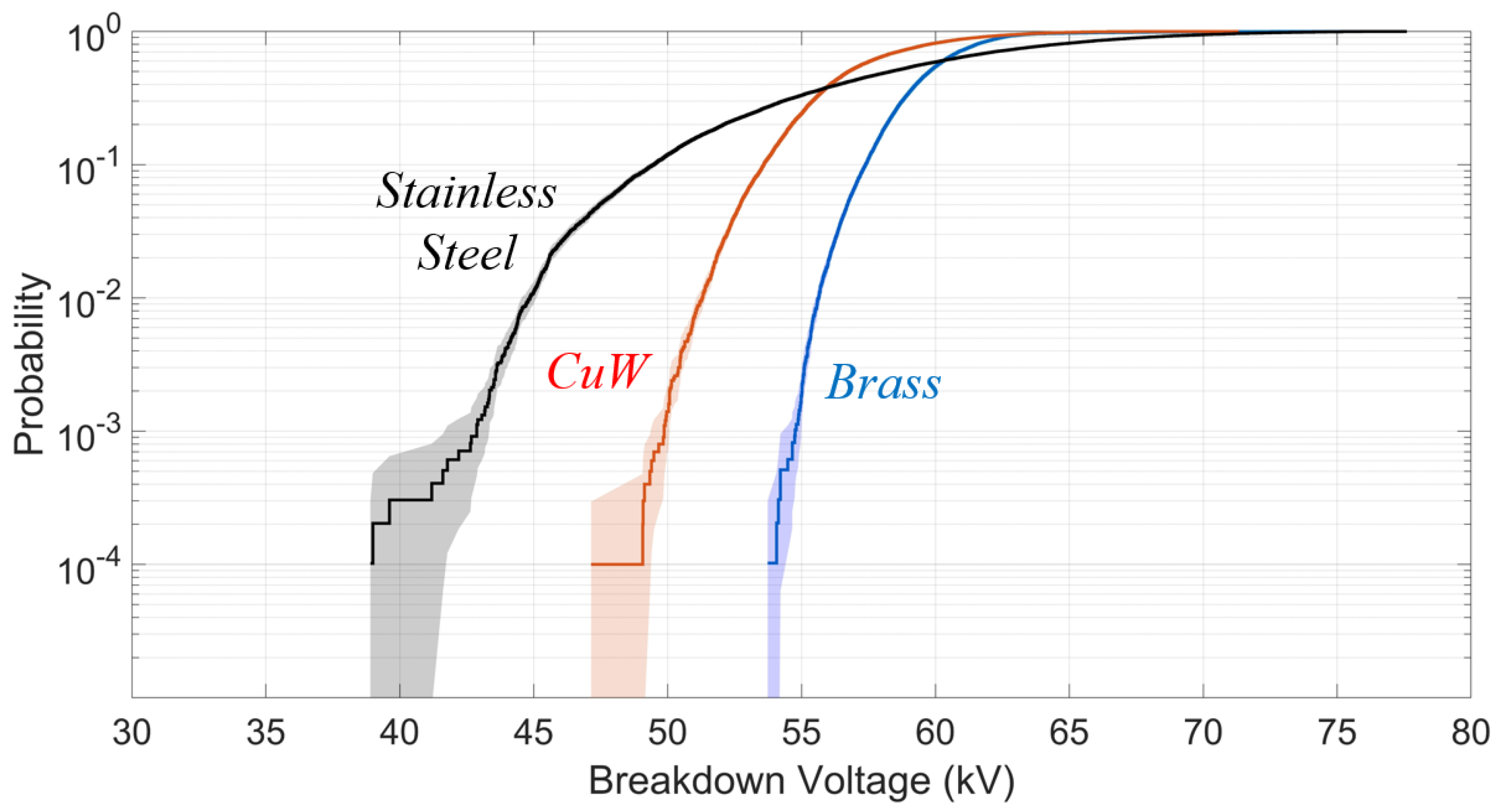
Each of the three materials investigated exhibits distinct breakdown voltage behavior, as reflected in the cumulative distribution functions presented in Figure 6. Beyond intrinsic material differences, caution is required when performing direct comparisons, owing to variations in gap spacing and the larger electrode dimensions employed for CuW. These design choices were necessary to accommodate the broader breakdown voltage distributions associated with stainless steel and CuW within the operational constraints of the test platform, and to maximize the use of CuW, which is comparatively limited in availability.
Notwithstanding these differences, meaningful comparisons of characteristic gap behavior and surface condition effects can be confidently made. The statistical measures summarized in Table 2 indicate that the relatively large standard deviations observed for stainless steel and CuW are likely to obscure more subtle differences arising from variations in gap configuration.
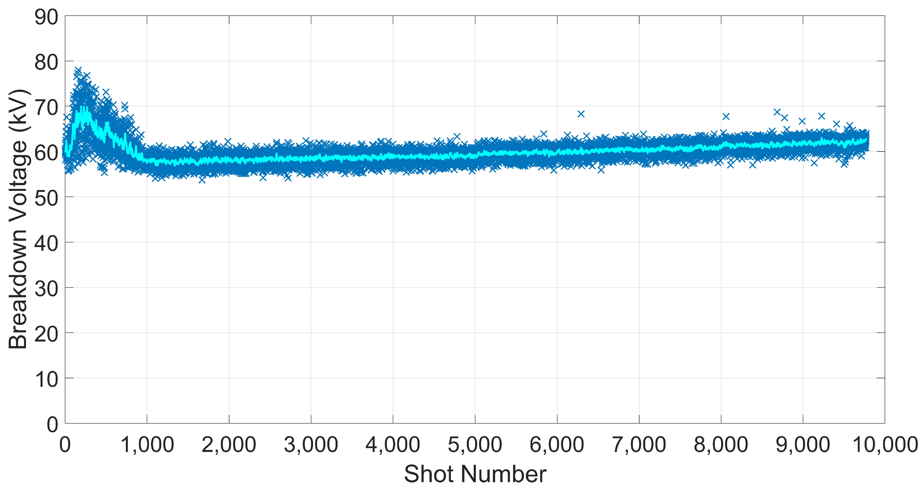
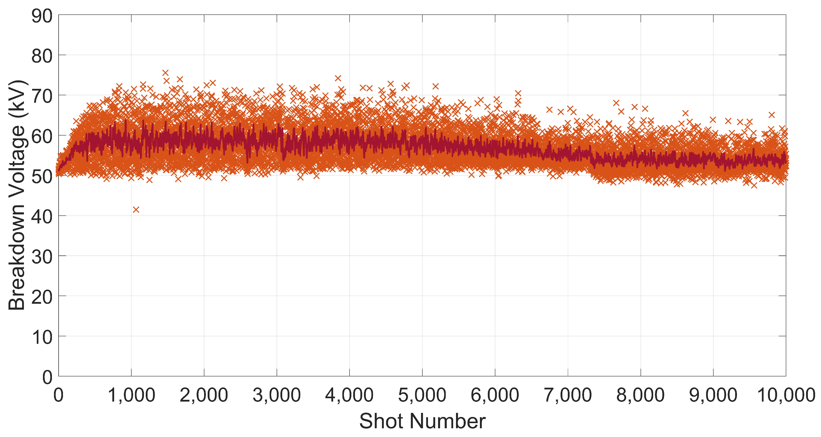
Brass electrodes are observed to transition through a phase of high variability, lasting approximately 1000 discharges from the last external perturbation, regardless of whether that is the start of an experiment or if it is due to maintenance of the actuated electrode connection. After this point, breakdown voltage variability decreases, with the average breakdown voltage exhibiting a noticeable linear increase across the remainder of the experiment as the electrodes wear, as seen in Figure 7. As with the other two materials tested, the changing performance of the electrodes in time means that fitting an experiment-wide statistical distribution must be done with care, particularly in the brass case, where a locally observed range of voltages spans a substantially smaller range than the full experiment.
CuW electrodes exhibit a similar initial variability to brass, but, as seen in Figure 8, do not exhibit the same pronounced stabilization, instead featuring a slow decrease in variability as the experiment progresses. Given the large size of the CuW electrodes relative to the brass and stainless steel electrodes, combined with their inherently superior erosion performance, it is reasonable to assume that the continued variability observed with CuW stems from the energy and charge transfer produced in these experiments being unable to produce uniform damage across the entire electrode.
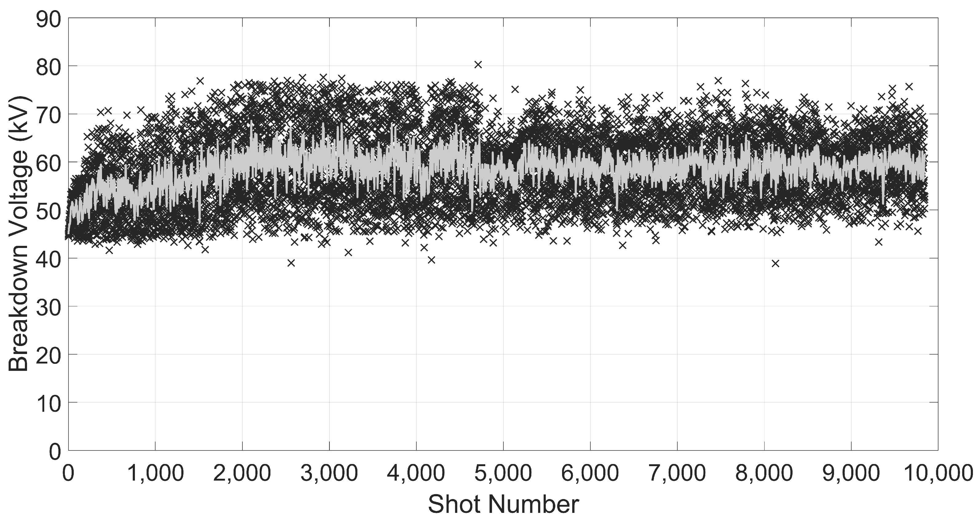
Stainless steel electrodes exhibit the highest variability in breakdown voltage, approaching a range of 40 kV, as well as the worst erosion performance of the materials tested. Despite this, no catastrophically low breakdown voltages, in which the switch closes at less than 60 percent of the nominal breakdown voltage, are observed. After approximately 5000 discharges, variability is observed to decrease, as seen in Figure 9.
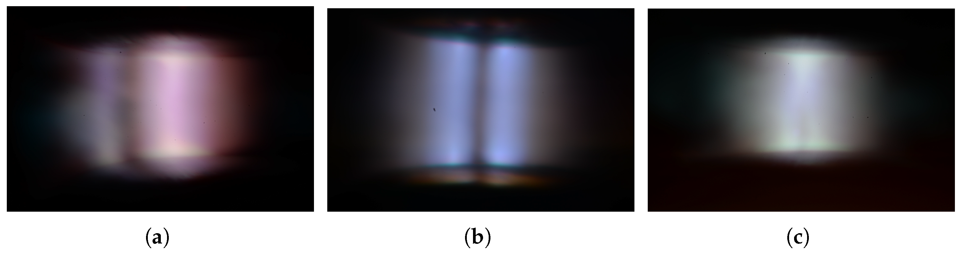
Interestingly, multiple spark channels are occasionally observed via the two discharge imaging cameras. This phenomenon is observed on CuW electrodes at a rate of approximately 4.5 discharges out of 1000, and at a rate of 40.7 out of 1000 for stainless steel, with no clear trends across experiments. Brass experiments can exhibit this phenomenon on as few as 0.7 of 1000 discharges, almost all of which occur during the initial variable portion of the switch’s lifetime. Multichanneling observed over the course of this work can be categorized into different archetypal observations. Two distinct channels spanning the length of the gap from electrode to electrode are most commonly observed; these channels may appear either similar or disparate in size, as seen in Figure 10, and the distance between the two channels range from near indistinguishably close together to far apart on opposite sides of the electrode, such as one of the two discharge images presented in Figure 3. Also observed are channels that split near an electrode, typically the cathode.
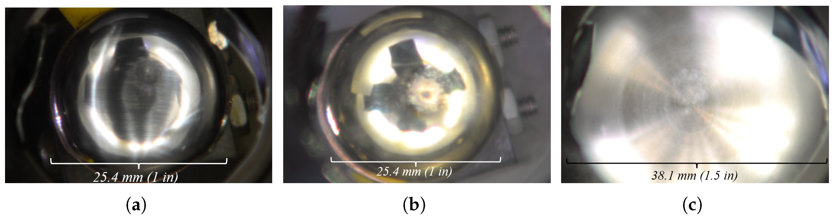
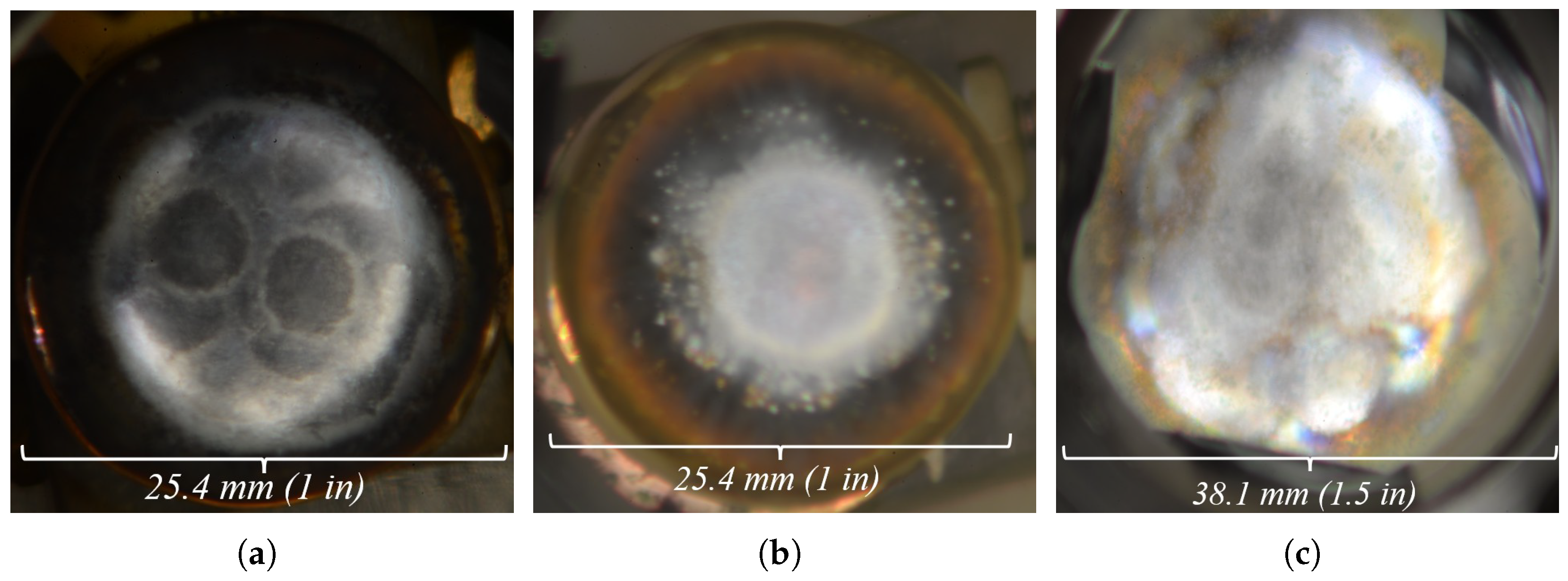
Qualitative analysis of the damage done to the electrodes in a single discharge can be performed by observing the surface images from after the first discharge, such as those in Figure 11, with the caveat that, as with any newly assembled switch, the breakdown voltage, and thus system energy and charge transfer, tends to be lower than average as the switch conditions in. Material-specific characteristics that will span the duration of the experiment are able to be observed from the first discharge. The damage crater left in stainless steel electrodes has a very pronounced crater rim versus the other two materials. Brass features a smaller crater relative to stainless steel, with a surrounding area characterized by an accumulation of larger metal droplets and particles; this is in contrast to the fine metal dust seen with stainless steel that, while not clearly evident on a single discharge, coats all surfaces in the vicinity of the electrodes over the course of an experiment. CuW exhibits visibly less damage than either of the two other materials, though the affected electrode surface area per discharge is similar.
Observing surface images taken after the final discharge in their respective experiment, it is evident that the entire uniform field area of the electrodes is utilized; however, as will be seen, the spatial distribution of breakdown locations on these electrodes is neither uniform nor random. Considering the images in Figure 12 as archetypal examples, the locations of recent plasma channel formation on stainless steel are made obvious by the pronounced damage craters left behind. Long-term damage in brass is characterized by a change in color, turning gray as erosion changes the metal composition; the most recently affected areas, which are more difficult to notice than in stainless steel due to their smaller size, take on a copper tint due to the selective removal of the other brass constituents as explained in Section Analysis of Electrode Microstructure and Surface Chemistry. Large particles away from the center of the affected area are still visible, as is an accumulation of finer dust. Both brass and stainless steel exhibit a ring of oxidized debris that accumulates around the uniform field area, which remains obvious on the cathode despite its repeated movement for imaging. CuW is visibly the least damaged of the three materials tested, with machining marks still visible towards the edges of the uniform field area, which are subjected to fewer discharges than the centers of the electrodes. Interestingly, despite exhibiting less visible damage, various locations of plasma channel formation are more obvious on CuW electrodes than on brass. Debris accumulation is less severe than on the other materials tested, which is surprising given the larger surface area of the CuW electrodes on which debris can accumulate, but which may be explained by the nature of how the CuW electrodes erode [1] versus the other two materials.
Analysis of surface images reveals similarities in the spatial distribution of plasma channels across the three tested materials. Upon visual inspection, it is clear that plasma channels tend to form in the immediate vicinity of the damage crater left behind by the previous discharge, often on or near the rim of that crater; this phenomenon is observable in the pair of successive surface images presented in Figure 5. Interestingly, for the roughly constant Coulomb transfer throughout the experiments, the damage crater radius is empirically observed to scale as ( k 1 / 10 T m e l t ) 1 , with k the thermal conductivity and T m e l t the melting temperature of the material, cf. Table 1. While suggestive of a fundamental thermal influence, this scaling remains phenomenological and may evolve with further exploration of the parameter space.
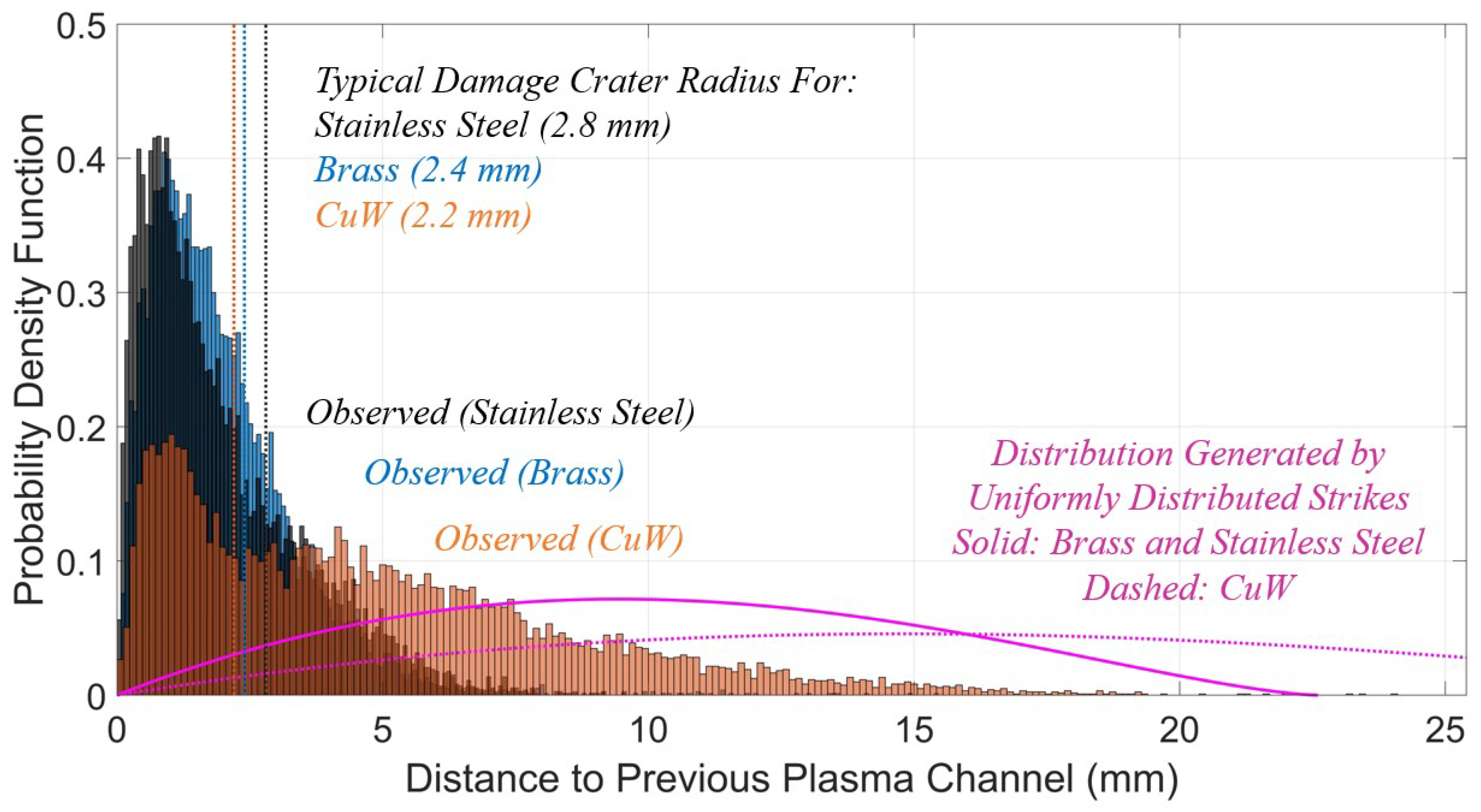
The preferential attachment of sparks to crater rims and pre existing damage is corroborated by post-processing complete experimental datasets, wherein the spatial separation between successive plasma channels is quantified. When these distances are presented as histograms, such as those in Figure 13, and compared against what would be expected from a uniform spatial distribution [30], it is clear that the spatial distribution of plasma channel formation on the electrode surfaces is nonuniform. The peaks of these spatial distributions are nonzero, instead appearing near a distance corresponding to the rim of the damage crater left behind by the previous discharge, as indicated in Table 3. In the case of the brass electrode, the mean of the distribution, 1.95 mm, falls approximately 0.5 mm inside the damaged area, typically 2.4 mm, inclusive of both the damage crater and surrounding debris, with the mode of the distribution, 0.89 mm, further within the damaged region. The mean of the distribution for the stainless steel electrode, 1.93 mm, falls further inside the 2.8 mm damaged region compared to brass, 0.9 mm vs. 0.5 mm, with the peak of the distribution, 0.79 mm, similarly falling closer to the center of the previous strike. Future plasma channels are, thus, dependent on damage done by the prior discharge, indicating that the electric field enhancement done by this damage can substantially affect the otherwise uniform macroscopic field. CuW distributions are occasionally observed to diverge slightly from the other two materials, with a double distribution such as the one presented in Figure 13, though unimodal distributions are also observed. Unlike for brass and stainless steel, the mean of the full distribution in Figure 13’s case, 4.76 mm, lies outside the typically damaged radius, 2.2 mm, though the mode of the tallest peak, found at 1.02 mm, lies within this range. This further substantiates the finding that damage-induced electric field enhancement affects the location of future breakdown, as the material that is visually least damaged has the widest spatial distribution across which the next breakdown may occur. Both visual inspection and computer analysis demonstrate that the entire uniform field region of the electrodes participates in discharges over the course of a long experimental run, but that uniform spatial utilization of the electrodes does not occur on short operational timescales, and is not necessarily guaranteed over the full lifetime of the electrode. This is logical, seeing as the damaged region created by a discharge spans a substantial portion of the uniform field area of the electrode, particularly for the smaller brass and stainless steel electrodes, such that some region near the center is likely to be damaged on each discharge. With Figure 13 demonstrating that the damage done by previous spark-surface interaction is likely to cause additional plasma channels to form near the same location, and taking into consideration the fact that the size of the damaged region means that areas near the center of the electrode are likely to be damaged, the result is a spatial preference towards the center, deviating from a uniform distribution.

Analysis of Electrode Microstructure and Surface Chemistry

Chemical analysis of the electrode surfaces is performed via energy-dispersive X-ray spectroscopy (EDS), which allows the surface composition of microscale features to be determined.
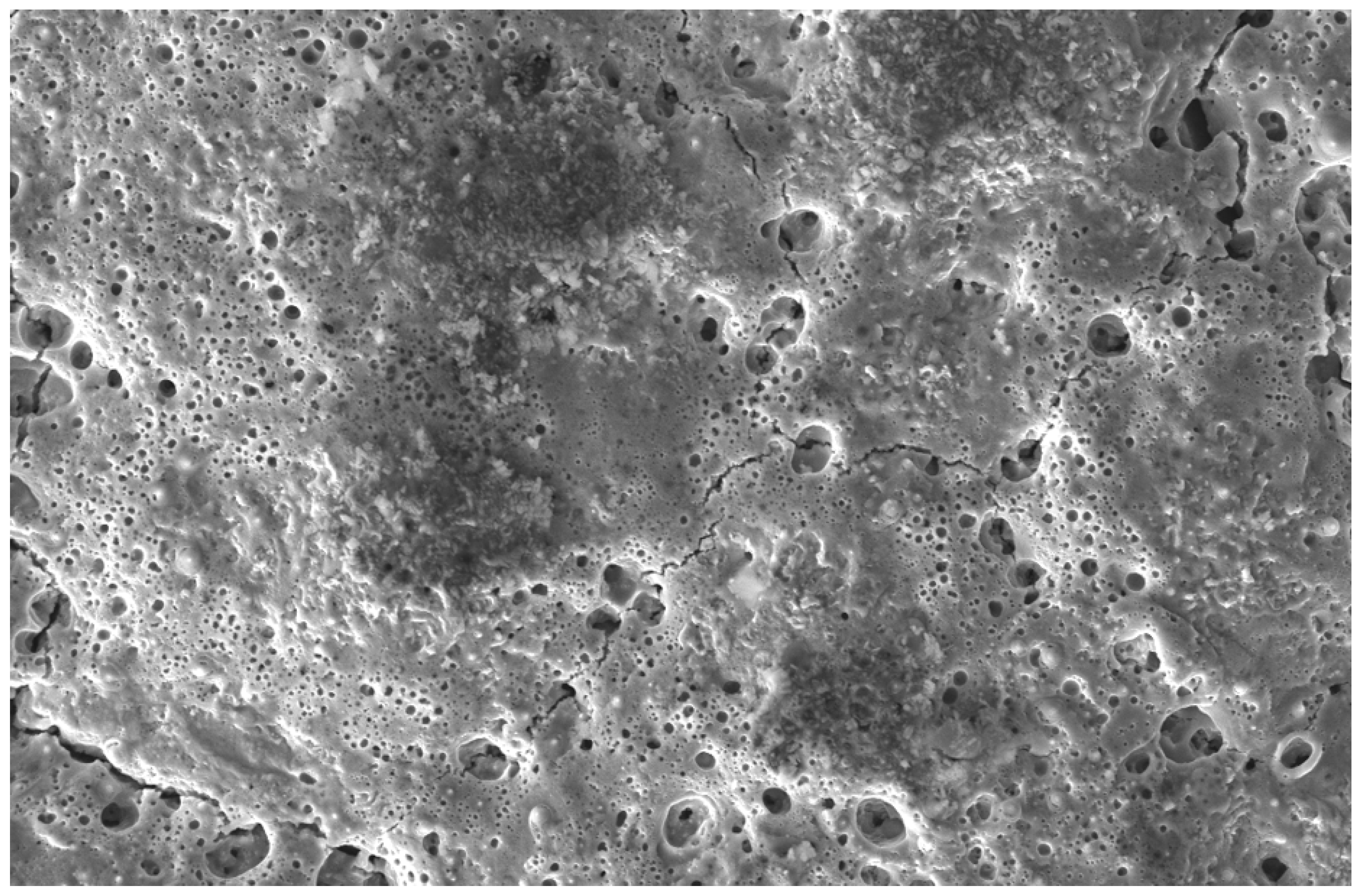
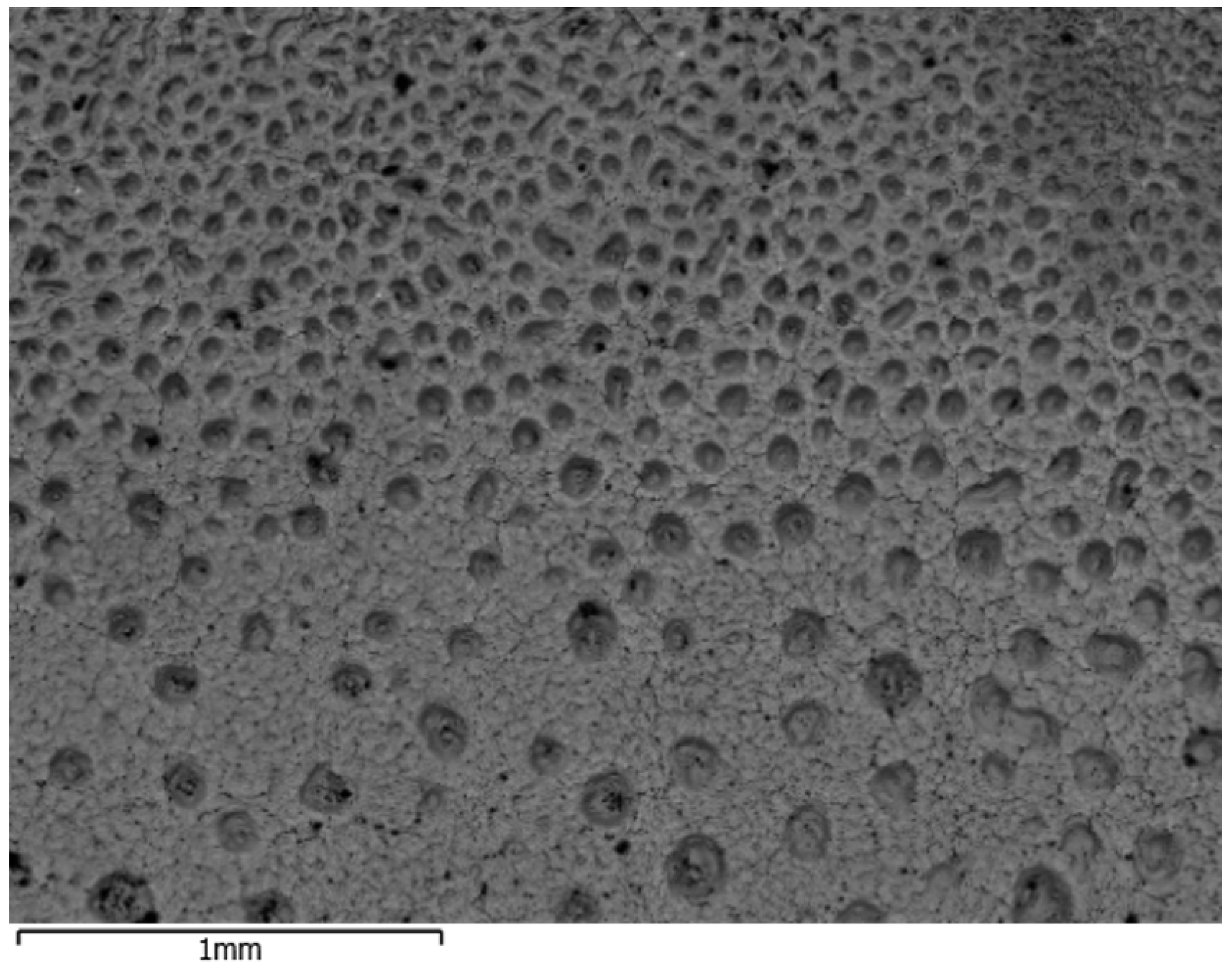
The primary motivation behind EDS studies has been to characterize the material removal seen using brass electrodes. Visual inspection of electrode surface images reveals copper coloring in the wake of a plasma channel, with the overall center region of the electrode taking on a gray-silver color, as seen in Figure 12. Away from the center is a black ring of debris accumulation, with additional debris accumulation continuing to the farther extremities of the electrode. EDS confirms that the copper tint is due to the preferential removal of the other, lower-melting-point constituent metals of the alloy where the plasma channel forms. Electron microscopy reveals molten copper resolidifying in grain boundaries, with porosity such as that in Figure 14, which suggests zinc and lead vapor escaping the molten metal, resulting in compositions such as the one presented in Table 4. This metal vapor is seen accumulating as droplets like those in Figure 15 towards the edges of the electrode, decreasing in size farther away from the center. Substantial oxide formation is noted, particularly in the black debris band, which is not observed on CuW electrodes. The prominence of carbon in these spectra is surprising given the lack of a spark gap body, but it is hypothesized to be due to the use of plastics as feedthroughs, in the moving electrode structure, and for debris mitigation within the pressure vessel. The appearance of carbon is supported by [31], which measured similar, if not slightly elevated carbon content on copper–tungsten electrodes, after repeated discharges in the vicinity of plastics. That carbon appears despite the lack of a spark gap body strongly suggests that future work must consider the effects of other materials present in the switch in greater detail, beyond the avoidance of switch body flashover.
Chemical composition notwithstanding, stainless steel electrodes exhibit similar features to their brass counterparts. The stainless steel electrode observed in Figure 16 has porosity similar to that of the brass electrode in Figure 14, again indicating that metal vapor is departing from a liquid surface, but visual inspection suggests that melting is taking place at a larger scale for stainless steel. EDS indicates substantial oxidization of the electrode surface occurs, with chromium oxides in particular forming in the grain boundaries as the surface melts and re-solidifies. Away from the center of the electrode, prominent pure metal features are observed atop the previously melted and oxidized surface. Given the size and lack of oxygen content in these features, it is hypothesized that they have a relatively short lifetime on the surface of the electrode, with their electric field enhancement likely contributing to the high variability in breakdown voltages observed for stainless steel, and that plasma chemistry is responsible for a significant amount of the observed oxidization. As seen in Table 4, stainless steel is the material that is most oxidized by mass, followed by CuW, then brass. Interestingly, this matches the sizes of the standard deviations presented in Table 2, suggesting that the electric field enhancement generated by triple points may contribute to the higher variability of stainless steel and CuW.
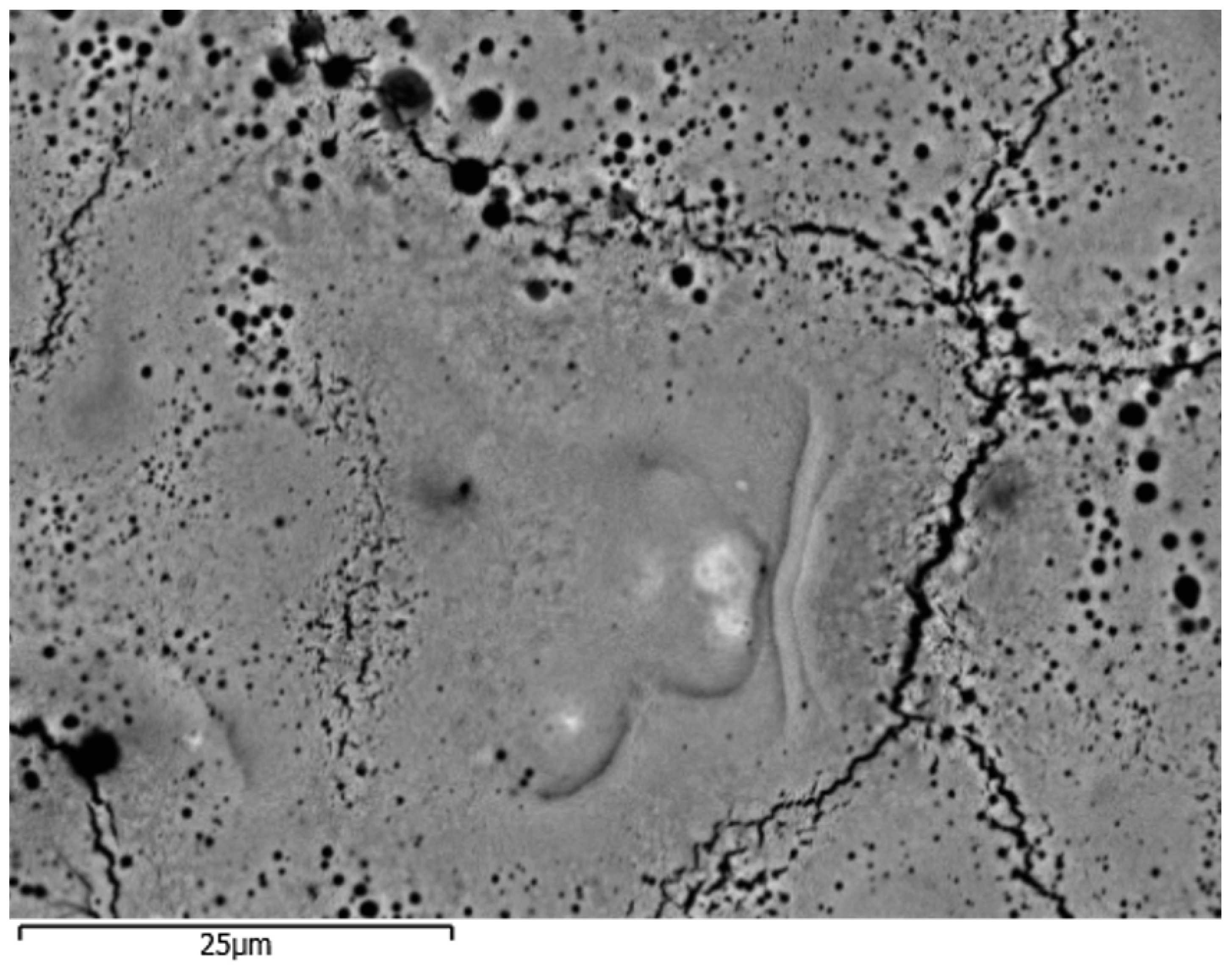
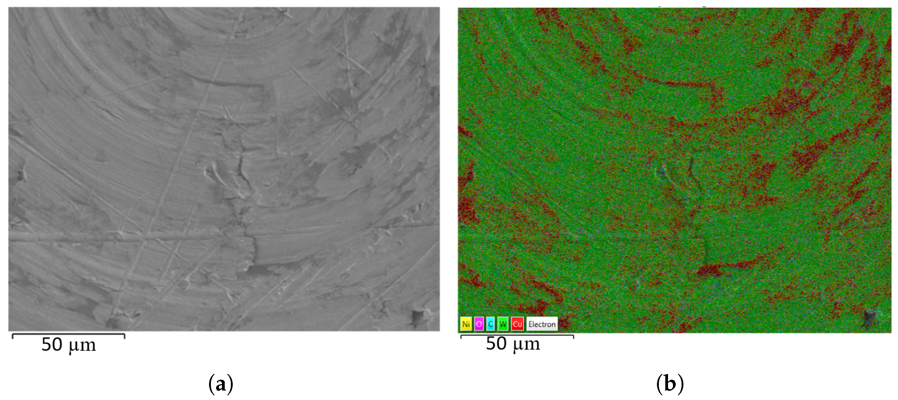
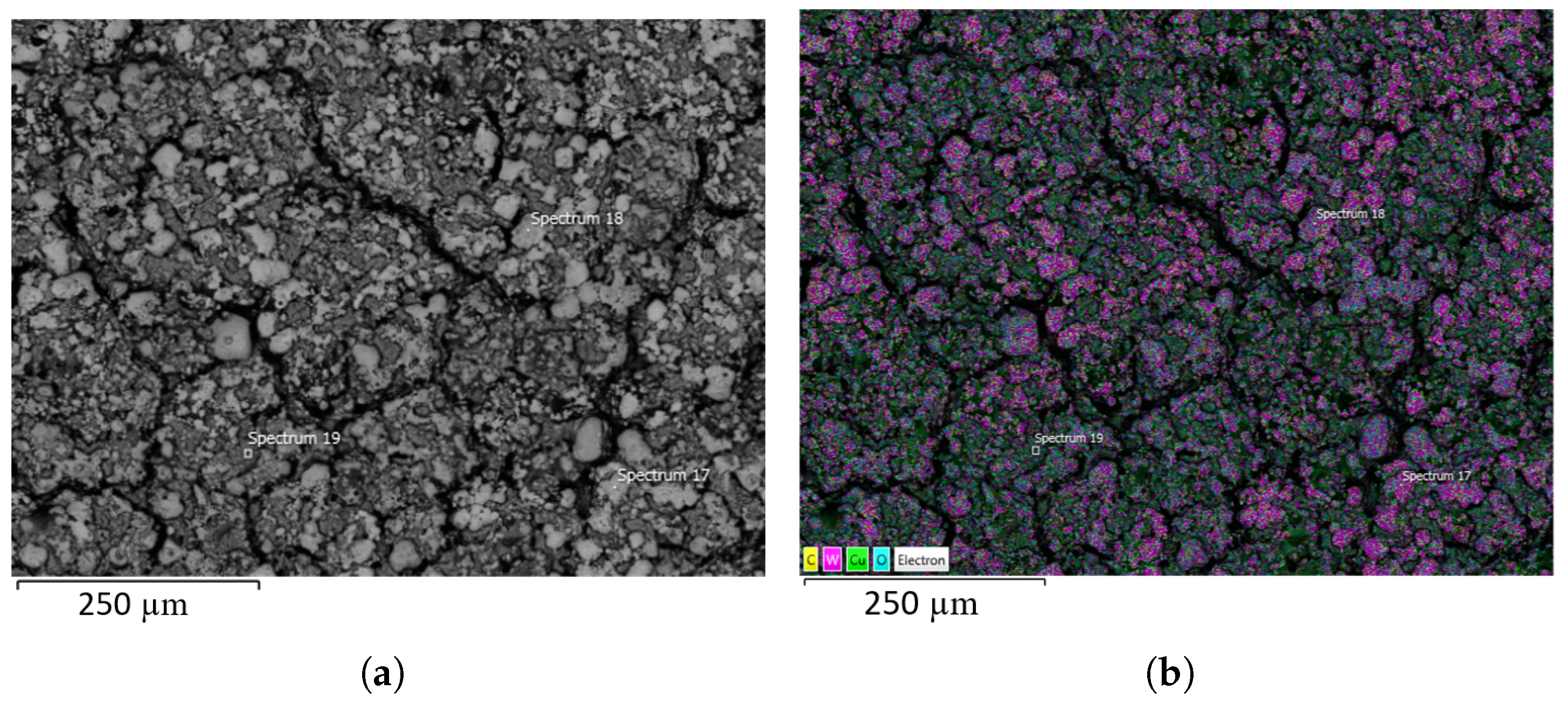
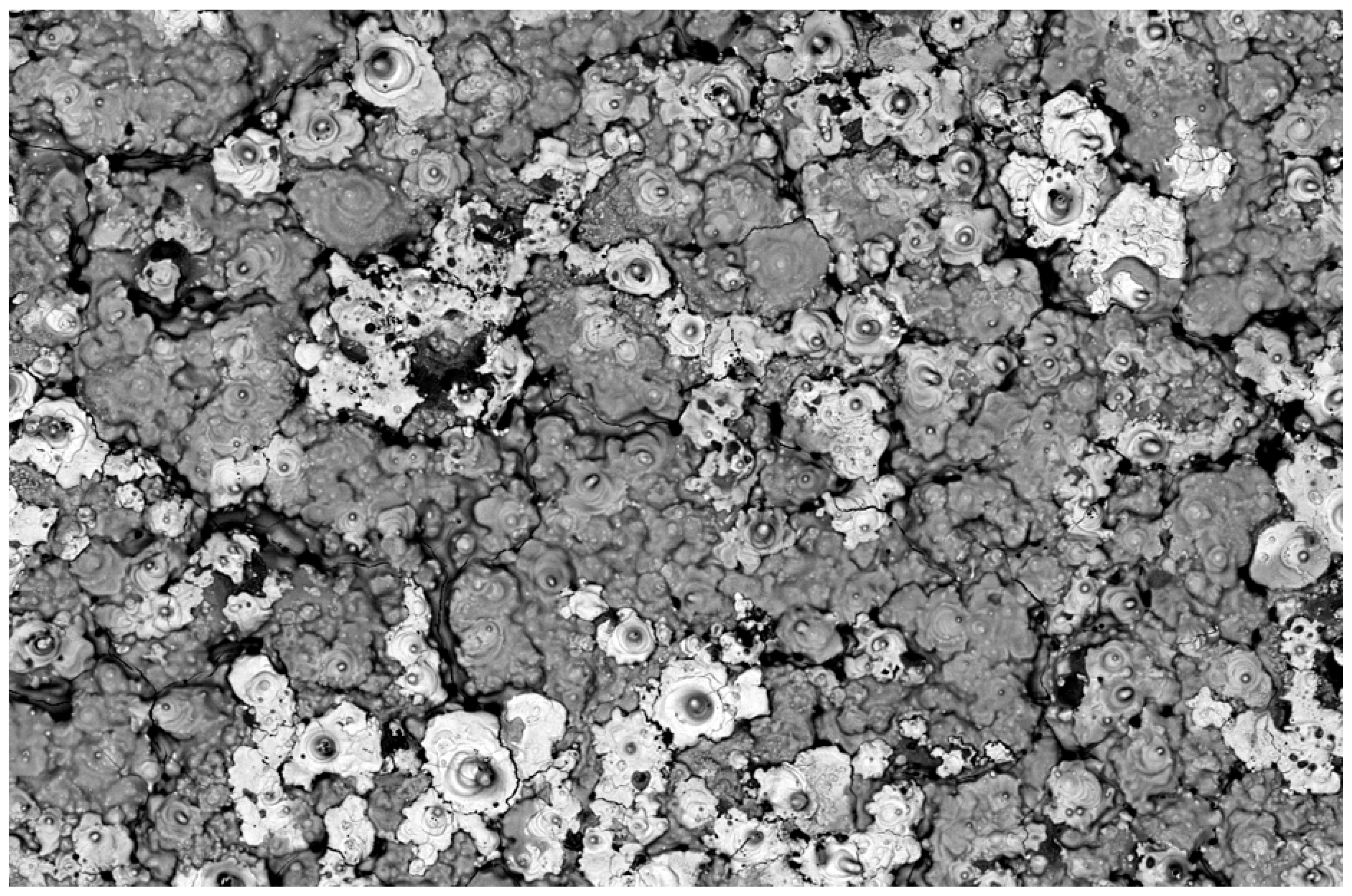
Given the nature of the CuW matrix, these electrodes are not polished prior to experimentation. EDS investigations prior to experimentation reveal regions of copper smeared over the underlying CuW substrate due to the machining process, as observed in Figure 17. After the experiment, the observed areas of the electrodes can be classified as looking at the center of the electrodes or the outer extremities of the electrodes. In the outer region of the CuW electrodes, scattered deposits of pure tungsten are observed atop the underlying base material. Pure deposits of copper, typically smaller than the tungsten deposits, can be found adjacent to the tungsten deposits, though never truly mixed, which is reasonable given the characteristics of the two elements. Moving towards the center of the electrode, as seen in Figure 18, pure deposits of each element are observed, trading smaller size for higher frequency as compared to deposits away from the electrode center. The appearance of pure tungsten is also observed in [32,33,34], albeit under substantially different experimental conditions. Evidence of both molten copper and molten tungsten can be seen, and the cracking structure seen at the center of these electrodes is hypothesized to be due to repeated melting and cooling, as opposed to a more traditional grain structure. These structures bear similarity to those observed in [31,33,34,35] despite the different CuW composition, switch gas, and electrical excitation between the bodies of work. The primary difference between the anode and cathode is microscale needle structures on the anode, depicted in Figure 19. These needles are composed of pure tungsten and are potentially due to the influence of gravity on molten tungsten over a series of discharge cycles.

4. Discussion

The lack of low voltage dropouts observed to date is somewhat surprising, and is currently hypothesized to be due to the lack of a midplane field-distortion trigger electrode or damage due to substantially higher Coulomb transfer, as seen in [9,36,37]. The sharp geometry of the midplane electrode is believed to be more adversely affected by wear and provide an additional point of failure for the gap. Of the relatively, but not critically, low voltage breakdowns that have been observed to date, surface imagery has been unable to identify a clear cause for the below-average performance, suggesting that the cause lies elsewhere. The surface images for these measurements bear no remarkable features when compared to their counterparts taken before and after expected breakdown voltages. The variability in breakdown voltage observed on CuW and stainless steel electrodes versus brass, demonstrated in Table 2, despite the absence of extremely low voltage events, stands in contrast to the deterministic expectations of Paschen’s Law. In reality, however, breakdown is inherently statistical rather than threshold driven, reflecting stochastic electron seeding and surface dependent effects. As reported in other studies of deviations from the Paschen curve [7,14], it is therefore hypothesized that local electric field enhancement at microscopic surface features, such as those in Figure 19, contributes significantly to the observed shot to shot variability. Occasional sharp features spread over a large area, thus, are suggested to account for the variability in CuW, while such features combine with the field enhancement contributed by oxide accumulation on stainless steel to result in more significant variance.
Beyond the choice of electrode material and configuration, spark gap switches span a variety of designs, use cases, and operating parameters, and future work is required to better understand the prevalence or lack thereof and cause of abnormal performance across this range. While the reasonably constant, approximately one discharge per minute, cycles seen on these experiments may not be out of place on future fusion energy research machines, such a cycle time is not identical to the nominally shot-per-day operations of the largest-scale high-energy-density research drivers. With others suggesting that pauses in operations may affect breakdown voltage performance [36], additional insight into how semi-continuous operation and associated gas chemistry affect switch reliability is necessary. Another notable real-world factor not considered in this work to date is the presence of a switch body. Given the nature of how imaging is performed during these experiments, complete enclosure of the spark gap inside a plastic or ceramic body is impossible. While debris-induced flashover of the spark gap body is typically treated as a separate failure mode from the premature gaseous breakdown investigated here, EDS observations tangentially suggest that the chemistry associated with plastic spark gap body decomposition may be worthy of future consideration. Future work includes filling the volume of large pressure vessels, such as the one presented here, with plastics in order to investigate the chemical contribution of plastic degradation to breakdown while avoiding switch failure due to body flashover.
Over the duration of this work, truly anomalous, potentially catastrophic low voltage breakdowns have been categorized as those which occur at less than 60 percent of the nominal self-breakdown voltage, implying that the pulsed power machine is being charged to a similar fraction of its switches’ self-breakdown voltage, and will be subsequently triggered from there by some means. Examples of machines that operate in a regime where this definition is valid can be found, notably Sandia’s Z Machine [38]; however, they tend to be dependent on intricate triggering schemes to ensure that reliable switch closure occurs despite the large disparity between the operating and self-breakdown voltages. At the time of writing, the largest deviations observed are switch closures at approximately three quarters of the nominal breakdown voltage, such as the one observed in Figure 8. While such an early closure would not pose substantial issues for a machine that can operate at nearly half of its switches’ self-breakdown voltage, one can easily imagine such an event being problematic for a machine running closer to self-breakdown. As such, one must take care to apply a reliability metric that suits the requirements of their application; while many pulsed power machines can operate with relaxed requirements compared to the Z scale metrics discussed in this work, future machines may need to impose even more stringent requirements.
Although no catastrophic low voltage breakdowns were observed in the present study, the long duration data acquired throughout these experiments are critically relevant to future fusion energy systems and high energy density physics drivers. Gradual changes in operating conditions that accumulate over thousands of shots will manifest on relatively short timescales in pulsed power driven fusion systems; consequently, such systems must be capable of rapidly adapting to evolving operating parameters to maintain stable and reproducible output.
As an illustrative example, consider a hypothetical fusion power plant operating at a repetition rate of 1 Hz. Under these conditions, the approximately 1000 shot interval of heightened variability shown in Figure 7 would correspond to a duration of roughly 17 min, followed by an increase in the mean self breakdown voltage of approximately 5 kV over the subsequent 2.5 h. While analogous changes would occur over longer timescales in single shot experimental drivers, the present results underscore the importance of long term performance characterization for ensuring output consistency and maintaining precise control of key electrical parameters.
It is worth emphasizing that the spatial distribution of spark events seen in Figure 13 is observed to be nonuniform across the nominally uniform region of the Rogowski profile electrodes. While the entire uniform field region is accessible, sparks preferentially form near the electrodes’ centers due to repeated initiation within or at the rims of existing damage craters. Because damage crater sizes are significant relative to the uniform field area, the central region is damaged on nearly every shot, increasing the probability of subsequent strikes there. Although sparks retain lateral mobility and lack the strong geometric focusing expected from conical or hemispherical electrodes, accumulated damage produces a distribution that is neither uniform nor truly random, even at scale. This suggests that one extracts the most benefits from a Rogowski profile if it is used over a long lifetime spanning thousands of shots; erosion benefits over a nonuniform field profile are unlikely to be seen over a small number of shots, as the plasma channels are likely to form near each other in both cases. This conclusion is further supported by this phenomenon being observed across all three electrode materials tested, as well as various electrode sizes and profiles. The spatial distributions observed on all materials tested suggest that one should expect worse electrode erosion performance and a shorter lifetime than would be achieved if wear were distributed evenly across the electrode surface.
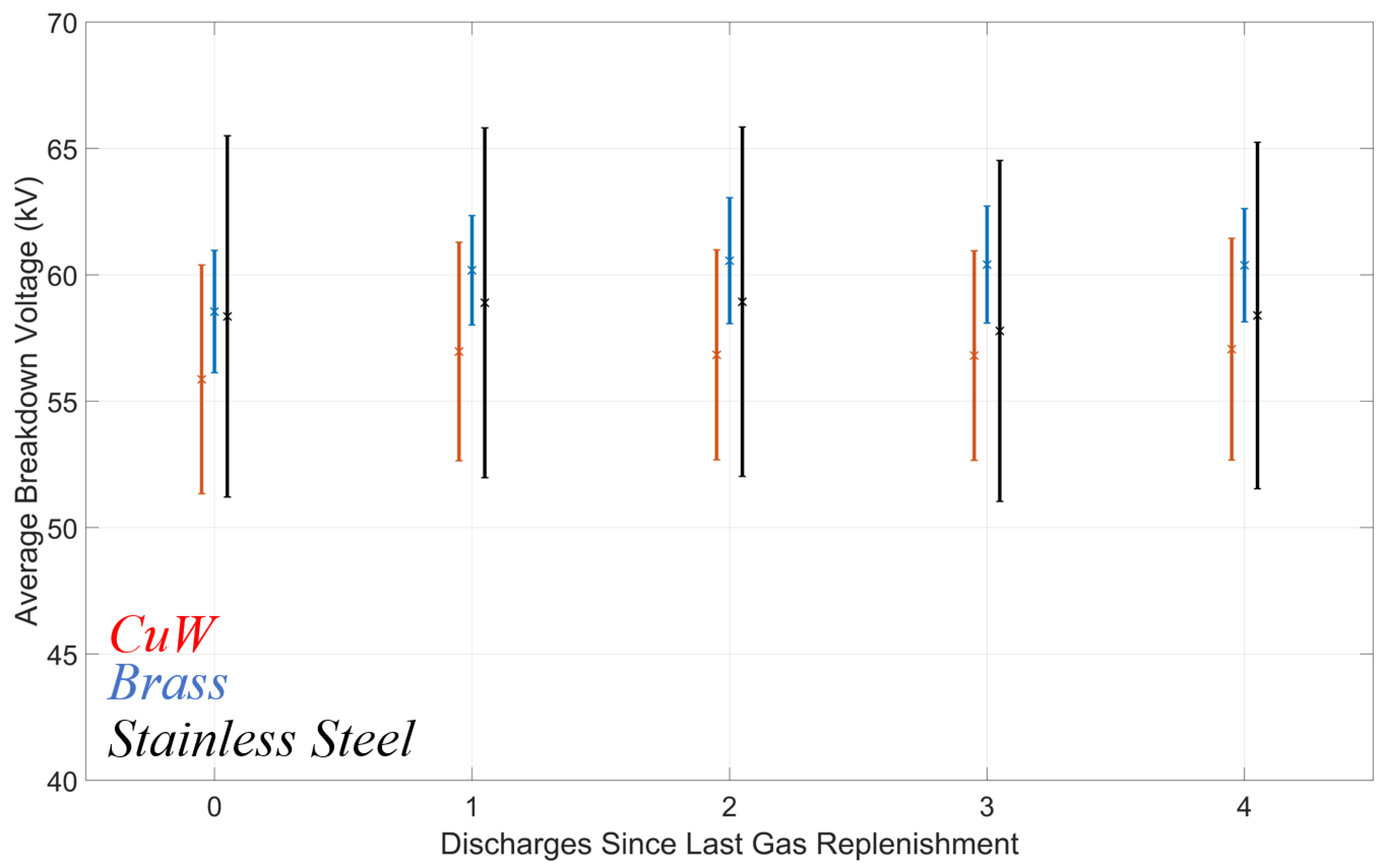
There are three key differences between the testbed used in this work and a traditional spark gap that must be considered when drawing comparisons to other work. The large, 17.4 L, volume of this pressure vessel is the largest limiting factor in comparing data from this testbed to other work. In contrast, the T-670 spark gap [16] has a measured volume of approximately 170 mL when its midplane electrode is removed. This volume disparity results in the relatively infrequent gas exchange described in Section 2.1, as more frequent exchange of such a large volume is not required, and would exhaust the available gas supply in an undesirably short time. As seen in Figure 20, neither the average breakdown voltage nor its variation is substantially affected by the gas replenishment interval. The large gas volume available to participate in subsequent switching events ensures that any gaseous products remaining within the pressure vessel between gas exchanges do not significantly affect breakdown voltage stability. The lack of a spark gap body also removes its associated failure modes and influence on switch gas chemistry, as discussed earlier in this section.
The other two key differences between this work and typical spark gap implementations are the actuated electrode and the relatively long and inductive electrical connections between the energy storage capacitors and the electrodes. While the abrupt nature of electrode actuation is able to occasionally disturb dust accumulation on the electrodes, the spatial distributions discussed in Section 3 suggest that this occasional disruption does not affect gap operation. In conjunction with the movement reproducibility described in Section 2.3, it is concluded that the actuated electrode does not prohibit comparison to a practical spark gap implementation. Both this actuated electrode and the pressure vessel needed to contain it result in electrical connections that are longer, and thus more inductive, than would be desired in a pulsed power machine. As the spark gap operation investigated in this work corresponds to the slow DC charging of initial energy storage stages of large pulsed power machines, this extra inductance is not considered to be detrimental to comparisons between this work and real-world spark gap implementations operating in the aforementioned use case, though comparison to spark gaps subjected to fast risetime or high frequency electrical stresses should be avoided.
Within this constrained, though non-negligible, range of test conditions, the materials examined can be systematically ranked in terms of their suitability for spark gap applications. Across most performance metrics, stainless steel emerges as the least favorable material; in fact, it was included primarily with the expectation that it might produce catastrophically low voltage discharges under conditions in which the other materials did not.
With respect to visible damage and electrode wear, the materials rank, from best to worst performance, as CuW, brass, and stainless steel. Although service life is ultimately application-dependent, it is reasonable to infer that the relative service life follows the same ordering as the observed damage and wear characteristics. When considering operational predictability, however, the ranking shifts to brass, followed by CuW, and then stainless steel, consistent with the standard deviation trends reported in Table 2. Cost and material availability represent the only criteria under which stainless steel does not rank lowest, owing to the comparatively high cost and limited availability of CuW relative to brass and stainless steel, both of which are readily accessible. Under this metric, the ranking from most to least favorable is stainless steel, brass, and finally CuW.


5. Conclusions

Long-lifetime electrode testing has been performed in order to better understand the cause of lower probability prefire events in spark gap switches. While the absence of high field enhancement midplane trigger electrodes appears to inhibit extremely low voltage breakdowns, the imaging capabilities fielded on these experiments reveal new information as to how spark gap surfaces are utilized and how their electrodes degrade over long periods of use. Future efforts to expand this work’s parameter space into different switch gases and electrode configurations will offer pulsed power system designers additional insights in order to create increasingly high-reliability systems.
Author Contributions

Conceptualization, A.S., J.S. and A.N.; methodology, L.B. and A.N.; software, L.B.; validation, J.S. and A.N.; formal analysis, L.B.; investigation, L.B. and R.C.; resources, A.S. and M.F.; data curation, L.B.; writing—original draft preparation, L.B.; writing—review and editing, R.C., J.S., A.S., M.F., J.M., J.D. and A.N.; visualization, L.B.; supervision, A.N.; project administration, A.S. and M.F.; funding acquisition, J.S., J.M., J.D. and A.N. All authors have read and agreed to the published version of the manuscript.

Funding

This work was supported by the Laboratory Directed Research and Development program at Sandia National Laboratories. Sandia is a multimission national laboratory managed and operated by National Technology and Engineering Solutions of Sandia LLC, a wholly owned subsidiary of Honeywell International, Inc., for the U.S. Department of Energy’s National Nuclear Security Administration under contract DE-NA0003525.

Data Availability Statement

Data are contained within the article.

Acknowledgments

The authors would like to thank Bo Zhao and the TTU College of Arts and Sciences Microscopy facility for lending their equipment and expertise to this work.

Conflicts of Interest

The authors declare no conflicts of interest.

Abbreviations

The following abbreviations are used in this manuscript:
CuWCopper–Tungsten
PPMParts Per Million
EMIElectromagnetic Interference
EDSEnergy-Dispersive X-Ray Spectroscopy
BSEBackscattered Electron
HEDHigh Energy Density

References

  1. Donaldson, A. Lifetime considerations. In Gas Discharge Closing Switches; Schaefer, G., Kristiansen, M., Guenther, A., Eds.; Plenum Press: New York, NY, USA, 1990; pp. 325–344. [Google Scholar]
  2. Stygar, W.; Awe, T.; Bailey, J.; Bennett, N.; Breden, E.; Campbell, E.; Clark, R.; Cooper, R.; Cuneo, M. Conceptual designs of two petawatt-class pulsed-power accelerators for high-energy-density-physics experiments. Phys. Rev. Spec. Top. Accel. Beams 2015, 18, 110401. [Google Scholar] [CrossRef]
  3. Cuneo, M.E.; Ampleford, D.J.; Austin, K.N.; Ao, T.; Brown, J.L.; Davis, J.P.; Biller, A.C.; Edens, A.D.; Harding, E.; Hutsel, B.T.; et al. The ZX initiative—An upgraded Z facility for eXtended performance, capabilities, and scientific impact. In Proceedings of the 2025 IEEE Pulsed Power and Plasma Science Conference, Berlin, Germany, 15–20 June 2025. [Google Scholar]
  4. Wan, Z.; Ding, W.; Sun, F.; Jiang, X.; Yuan, Q. Characteristics of the output voltage generated by switch prefire in multistage linear transformer drivers. IEEE Trans. Plasma Sci. 2024, 52, 1398–1405. [Google Scholar] [CrossRef]
  5. Donaldson, A.; Hagler, M.; Kristiansen, M. Electrode erosion in a high energy spark gap. In Proceedings of the 4th IEEE International Pulsed Power Conference, Albuquerque, NM, USA, 6–8 June 1983. [Google Scholar]
  6. Kristiansen, M.; Hagler, M.; Donaldson, A.; Ness, R. Surface studies of electrodes used in spark gaps. In Proceedings of the 4th IEEE International Pulsed Power Conference, Albuquerque, NM, USA, 6–8 June 1983. [Google Scholar]
  7. Donaldson, A.; Hagler, M.; Kristiansen, M.; Hatfield, L.; Ness, R. Modeling of self-breakdown voltage statistics in high-energy spark gaps. J. Appl. Phys. 1985, 57, 4981–4990. [Google Scholar] [CrossRef]
  8. Song, F.; Li, F.; Zhang, B.; Zhu, M.; Li, C.; Wang, G.; Gong, H.; Gan, Y.; Jin, X.; Novac, B.M.; et al. Electrode erosion and lifetime performance of a compact and repetitively triggered field distortion spark gap switch. IEEE Trans. Plasma Sci. 2020, 48, 212–218. [Google Scholar] [CrossRef]
  9. Li, X.; Pei, Z.; Ma, C.; Zhang, Y.; Zhang, Q. Prefire properties of high pressure gas spark switches for fast linear transformer drivers. IEEE Trans. Plasma Sci. 2018, 46, 4099–4108. [Google Scholar] [CrossRef]
  10. Khairi, A.; Shumlak, U. Experimental investigation of plasma-electrode interactions on the ZaP-HD sheared-flow-stabilized Z-pinch device. Phys. Plasmas 2026, 33, 032503. [Google Scholar] [CrossRef]
  11. Sun, J.; Qing, Q.; Liu, H.; Yao, X.; Jiao, Z.; Wu, Y. A compact high-stability nanosecond pulse test system using corona-stabilized switch and coaxial resistance divider. Energies 2023, 16, 4534. [Google Scholar] [CrossRef]
  12. Gandi, V.; Verma, R.; Warrier, M.; Sharma, A. Effect of electrode profile and polarity on performance of pressurized spark gap switch. Plasma 2022, 5, 130–145. [Google Scholar] [CrossRef]
  13. Zhang, Y.; Zhang, J.; Li, J.; Zhang, X.; Jia, Y.; Li, Q.; Wang, J.; Ren, H. Arc erosion characteristics of functional gradient/copper-tungsten contacts: Cellular automaton simplification methods and applications. IEEE Trans. Plasma Sci. 2025, 53, 3668–3678. [Google Scholar] [CrossRef]
  14. Luo, W.; Cong, P.; Huang, T.; Zhai, R.; Qiu, A. Calculation model of self-breakdown voltage distribution in gas switches. IEEE Trans. Plasma Sci. 2018, 47, 4335–4341. [Google Scholar]
  15. Luo, C.; Cong, P.; Zhang, T.; Zhong, X.; Luo, W. Prediction and experimental verification of erosion resistance of gas switch electrode materials. AIP Adv. 2021, 11, 055206. [Google Scholar] [CrossRef]
  16. L3 Communications Applied Technologies Pulse Sciences. Series T-670 High Precision Spark Gap Switches; T-670/IND/2002/11; L3 Communications Applied Technologies Pulse Sciences: San Leandro, CA, USA, 2002. [Google Scholar]
  17. L3 Communications Applied Technologies Pulse Sciences. Series T-508 High Precision Spark Gap Switches; L3 Communications Applied Technologies Pulse Sciences: San Leandro, CA, USA, 2002. [Google Scholar]
  18. Martin, T. An empirical formula for gas switch breakdown delay. In Proceedings of the 7th IEEE Pulsed Power Conference, Monterey, CA, USA, 11–14 June 1989. [Google Scholar]
  19. Boswell, L.; Jakob, M.; Jacob, S.; Steiner, A.; Neuber, A. An apparatus to investigate electrode surface condition effects on spark gap reliability. In Proceedings of the 2025 IEEE Pulsed Power and Plasma Science Conference, Berlin, Germany, 15–20 June 2025. [Google Scholar]
  20. Tungsten-Based Composites. Available online: https://www.plansee.com/en/materials/w-mmc.html (accessed on 15 January 2026).
  21. Rogowski, W. Die elektrische Festigkeit am Rande des Plattenkondensators: Ein Beitrag zur Theorie der Funkenstrecken und Durchführungen. Arch. Elektrotechnik 1923, 12, 1–15. [Google Scholar] [CrossRef]
  22. Trinh, N. Electrode design for testing in uniform field gaps. IEEE Trans. Power Appar. Syst. 1980, 99, 1235–1242. [Google Scholar] [CrossRef]
  23. AMS5501G; Steel, Corrosion-Resistant, Sheet, Strip, and Foil 19Cr—9.5Ni (304) Cold Rolled, 125 ksi (862 MPa) Tensile Strength. SAE International: Warrendale, PA, USA, 2025.
  24. Stainless Steel AISI 304L. Available online: http://esmat.esa.int/Services/Preferred_Lists/Materials_Lists/a62.htm (accessed on 16 April 2026).
  25. B16/B16M-24; Standard Specification for Free-Cutting Brass Rod, Bar, and Shapes for Use in Screw Machines. ASTM International: West Conshohocken, PA, USA, 2024.
  26. 360 Brass Product Guide. Available online: https://www.onlinemetals.com/en/product-guide/alloy/360?srsltid=AfmBOoqqDCzJlbqewRvadVzGwYDfDgFuTGfasoD-zHxrYzrY1k_ZTwPY (accessed on 16 April 2026).
  27. Tungsten-Copper for Use in Circuit Breakers. Available online: https://www.plansee.com/en/products/wcu-switching-contacts.html (accessed on 15 January 2026).
  28. Stainless 304 Product Guide. Available online: https://www.onlinemetals.com/en/product-guide/alloy/304 (accessed on 7 May 2026).
  29. Melting Points of Metal. Available online: https://www.onlinemetals.com/en/melting-points?srsltid=AfmBOoqkXfFKtyKfavViDgd39cQH1hbo6YELLbdwMJF-121Ft0tB5vVP (accessed on 7 May 2026).
  30. Mathai, A. An Introduction to Geometrical Probability Distributional Aspects with Applications; Gordon and Beach Science Publishers: Amsterdam, The Netherlands, 1999. [Google Scholar]
  31. Gordon, L.; Kristiansen, M.; Hagler, M.; Kirbie, H.; Ness, R.; Hatfield, L.; Marx, J. Material studies in a high energy spark gap. IEEE Trans. Plasma Sci. 1982, 4, 286–293. [Google Scholar] [CrossRef][Green Version]
  32. Slade, P.; Li, W.; Loud, L.; Haskins, R. The unusual electrode erosion of high tungsten content, tungsten copper contacts switching load current in vacuum. IEEE Trans. Compon. Packag. Technol. 2001, 24, 320–330. [Google Scholar] [CrossRef]
  33. Zhou, Y.; Humphries, J.; Spencer, J.; Yan, J.; Wang, Z.; Jones, G. Contact erosion at high currents in high-voltage gas circuit breakers—Part 1: Experimental research and material testing. IEEE Trans. Power Deliv. 2025, 40, 776–785. [Google Scholar] [CrossRef]
  34. Zhang, P.; Xie, H. Erosion behaviour of WC and Cu-WC contact materials under vacuum arc. JOM 2025, 77, 8416–8425. [Google Scholar] [CrossRef]
  35. Wang, X.; Wei, S.; Zhang, C.; Xu, L.; Yu, H.; Yang, L.; Pan, K.; Wang, H.; Cao, X. Arc erosion property and mechanism of tungsten-copper alloy with multi-scale tungsten particles. J. Mater. Sci. 2024, 59, 1635–1651. [Google Scholar] [CrossRef]
  36. Burnette, M.; Smith, J. Investigation of the longevity of high voltage switches in various gases. In Proceedings of the 2025 IEEE Pulsed Power and Plasma Science Conference, Berlin, Germany, 15–20 June 2025. [Google Scholar]
  37. Wu, J.; Han, R.; Ding, W.; Wang, Y.; Yan, J.; Qiu, A. Experimental study of self-breakdown voltage statistics in Cu-W electrode spark gap switches. IEEE Trans. Dielectr. Electr. Insul. 2017, 24, 2056–2065. [Google Scholar] [CrossRef]
  38. Savage, M.E.; Austin, K.N.; Hutsel, B.T.; Kamm, R.J.; McKee, G.R.; Stygar, W.A.; Wakel, P.E.; Wemple, N.R.; White, W.M. Pulsed power performance of the Z machine: Ten years after the upgrade. In Proceedings of the 2017 IEEE International Conference on Pulsed Power, Brighton, UK, 18–22 June 2017. [Google Scholar]
Figure 1. A typical current waveform and charge transfer observed during lifetime experiments. This discharge occurred at a breakdown voltage of approximately 59 kV, resulting in a peak current and charge transfer of approximately 11 kA and 0.11 C, respectively.
Energies 19 03043 g001
Figure 2. An annotated schematic of the high voltage system. Constant current is fed via a pair of high voltage power supplies to capacitor banks, two pairs of 2.2 μ F capacitors in series balanced by 100 M Ω resistors, resulting in a linear voltage increase of ±1 kV/s. High voltage relays clear residual energy between discharges and divert stored charge to dump resistors during faults. Gap closure directs current through series discharge resistors that set the capacitor bank charge transfer. The illustrated discharge path parasitic inductance is inferred from matching simulations to measured waveforms.
Energies 19 03043 g002
Figure 3. Typical discharge images and the computer-generated reconstruction of the observed plasma channels. (a) The X-axis image, in which the plasma channels are oriented such that only a single channel is visible. The post-processed approximation of the plasma channel’s center is overlaid in green. (b) The Y-axis image of the same discharge, whose orthogonal view to the X-axis reveals an otherwise hidden second plasma channel. Post-processed approximations of the two plasma channel centers are overlaid in green. (c) The computer reconstruction of the plasma channels, generated by combining data from (a,b), with dimensions in millimeters, with the circular projection of the electrode surfaces plotted. These images are captured from an experiment using 38.1 mm (1.5 inch) diameter CuW electrodes, with an 8 mm gap distance; the difference in channel color between the two images is due to different camera settings.
Energies 19 03043 g003
Figure 4. Annotated cross sections of CAD representations of the interior of the pressure vessel, with the moving electrode and piston (a) positioned for discharge, and (b) positioned to image electrode surfaces, with the piston assembly cropped for clarity. Motion between the two positions is made possible by the piston housed in the extension on the right of the pressure vessel. The second window used to image the discharge is off the page from this depiction. The surface imaging mirrors and moving electrode to feedthrough cable are omitted to preserve presentation clarity.
Energies 19 03043 g004
Figure 5. Typical surface images and computer analysis of damage done to a stainless steel cathode. Computer analysis requires a pair of images taken (a) before and (b) after a discharge. The image pair is converted to grayscale, and the pre-discharge image is subtracted from the post-discharge image. Nominally, only information about the discharge site and other affected areas remains at this point. The image is then thresholded, at which point region detection can occur to create (c), in which the bounding boxes of detected regions are overlaid upon the thresholded image. Finally, additional filtering and, if necessary, linking of overlapping regions occurs in order to determine the center of the damaged area, presented in (d) as an overlay onto (b).
Energies 19 03043 g005aEnergies 19 03043 g005b
Figure 6. Cumulative distribution plots for the data presented in Figure 7, Figure 8 and Figure 9. Brass data are presented in blue, CuW in red, and stainless steel in black. The shaded regions represent the 95 percent confidence interval for their respective data. Given the differences in gap distance and electrode material across these experiments, it would be unreasonable to expect identical statistical distributions.
Energies 19 03043 g006
Figure 7. Recorded breakdown voltages observed for a pair of brass electrodes presented in order of occurrence, with a 10-discharge moving average overlaid. The initial gap distance is set to approximately 8 mm (0.32 in), with the pressure vessel filled with dry air at 248 kPa absolute pressure (36 psia).
Energies 19 03043 g007
Figure 8. Same as Figure 7, but with CuW electrodes and the initial gap distance set to approximately 7.5 mm (0.3 in). Note the low voltage observation, approximately 41.5 kV, does not reach the 60 percent of nominal operating voltage threshold, but is the closest of all observed datapoints to that threshold.
Energies 19 03043 g008
Figure 9. Same as Figure 7, with stainless steel electrodes and the initial gap distance set to approximately 6.5 mm (0.26 in). While variation remains high, some stabilization is noted to occur slightly beyond halfway through the experiment.
Energies 19 03043 g009
Figure 10. Archetypal images of multiple plasma channels captured during single discharges across several experiments. Plasma channels tend to exhibit either the notable asymmetry in size and luminosity observed in (a), or appear as a pair of similarly sized channels seen in (b). Less frequently, a channel may split near an electrode, such as in (c), where the channel splits near the cathode. The shape of the plasma channels observed in (b) is corroborated by oval-shaped damage crater pairs in the associated surface images, with the current-induced magnetic field pulling the channels towards each other.
Energies 19 03043 g010
Figure 11. Surface images after a single discharge for (a) stainless steel, (b) brass, and (c) CuW electrodes.
Energies 19 03043 g011
Figure 12. Surface images of the electrodes presented in Figure 11 after their respective experiments for (a) stainless steel, (b) brass, and (c) CuW electrodes, with regions away from the electrodes cropped to preserve detail.
Energies 19 03043 g012
Figure 13. Probability density functions of the distances between successive plasma channels on each of the three materials tested. The nominal affected radius for each electrode is depicted as vertical dashed lines at 2.2 mm, 2.4 mm, and 2.8 mm for CuW, brass, and stainless steel, respectively. The probability density functions that would be created by uniform spatial utilization of the electrode surfaces’ uniform field regions are depicted by the solid magenta line for stainless steel and brass, and by the dashed line for the larger diameter CuW electrode. Please note that in addition to diverging from uniform spatial distributions, the peaks of the observed spatial distributions, 0.79 mm for stainless steel, 0.89 mm for brass, and 1.02 mm for CuW, each fall within the typical damage crater radius for the relevant material. The means of the three distributions are 1.93 mm for stainless steel, 1.95 mm for brass, and 4.76 mm for CuW.
Energies 19 03043 g013
Figure 14. An electron microscope image of a brass electrode after experimentation. The bubbles on the surface suggest metal vapor evaporating from a molten metal surface during discharges over the course of the experiment. The width of the image spans approximately 166 μ m.
Energies 19 03043 g014
Figure 15. Condensed metal droplets forming away from the center of a brass electrode. The edge of the electrode is towards the top of the image, with droplets becoming smaller the farther away they are located from the center.
Energies 19 03043 g015
Figure 16. An electron microscope image of the center of a stainless steel anode after experimentation. Microscopy reveals porosity similar to that of brass, with evidence of more substantial melting and re-solidification.
Energies 19 03043 g016
Figure 17. (a) An electron microscope image of the as-machined surface of a CuW electrode prior to experimentation. While EDS indicates that the appropriate 80 percent tungsten, 20 percent copper is maintained at a macroscopic scale, the manufacturing process results in copper smearing over tungsten, as observed in (b), in which the elements detected by EDS are overlaid onto (a). Tungsten is depicted in green, while copper appears as red.
Energies 19 03043 g017
Figure 18. (a) An electron microscope image of the center of a CuW cathode after experimentation. Local EDS spectra at the highlighted points indicate that the droplets that form atop the underlying material are tungsten, which has been melted if not vaporized, and then re-solidified. The separation of copper and tungsten is also evident on visual inspection of (b), the EDS element detection overlay of the image presented in (a). The damage done to the center of the electrode is such that the original stair step pattern left behind by the machining process has been destroyed and is no longer visible.
Energies 19 03043 g018
Figure 19. Backscattered electron (BSE) microscopy image of a CuW anode surface after experimentation. Heavier elements appear brighter on the BSE image, implying that the observed needlepoints are composed of tungsten, which is confirmed by EDS analysis. The width of the image spans approximately 500 μ m.
Energies 19 03043 g019
Figure 20. Average breakdown voltages for the data presented in Figure 6, Figure 7, Figure 8 and Figure 9 versus the number of discharges since the switch gas in the pressure vessel has been replenished. The error bars correspond to the standard deviation of the associated datapoint.
Energies 19 03043 g020
Table 1. Select properties of the materials tested in this work. Created using data from [20,23,24,25,26,27,28,29].
MaterialElectrical Conductivity
(S/ μ m)
Thermal Conductivity
(W/(m∗K))
Melting Point (°C)Composition by Weight
304L Stainless Steel1.3916.21400–145518–20% Cr, 8–11%
Ni, remainder Fe
360 Brass15.8115890–90060–63% Cu, 2.5–3%
Pb, remainder Zn
CuW16250 11084 (Cu)
3400 (W)
80% W, 20% Cu
1 Volume averaged thermal conductivity, actual conductivity may be lower due to interfacial thermal resistance.
Table 2. Breakdown voltage statistics for the data presented in Figure 6, Figure 7, Figure 8 and Figure 9.
MaterialAverage Breakdown Voltage (kV)Standard Deviation (kV)
Brass60.012.45
CuW56.714.33
Stainless Steel58.476.93
Table 3. Key values of the probability density functions presented in Figure 13.
MaterialMean (mm)Peak (mm)Typical Damage Radius (mm)
Brass1.950.892.4
CuW4.761.022.2
Stainless Steel1.930.792.8
Table 4. EDS determined compositions after experimentation. All EDS spectra presented in this table are captured from archetypal regions near the center of their respective electrodes. All compositions are presented as mass percentages.
MaterialElementAnode Mass PercentageCathode Mass Percentage
BrassCu76.571.1
Zn8.610.6
O7.37.3
C7.110.3
Pb0.50.5
Fe0.10.1
Stainless SteelFe52.655.3
O2219.9
Cr16.616.8
Ni4.14.3
C3.32.6
Mn1.21.1
Si0.20
CuWW66.866.4
Cu1317.4
O12.310.6
C85.6
Disclaimer/Publisher’s Note: The statements, opinions and data contained in all publications are solely those of the individual author(s) and contributor(s) and not of MDPI and/or the editor(s). MDPI and/or the editor(s) disclaim responsibility for any injury to people or property resulting from any ideas, methods, instructions or products referred to in the content.