Article

Dynamic Compensation for Constant-Voltage WPT with Non-Uniform Windings and Parasitic Coils

State Key Laboratory of Smart Power Distribution Equipment and System, Hebei University of Technology, Tianjin 300401, China
*
Author to whom correspondence should be addressed.
Energies 2026, 19(12), 2925; https://doi.org/10.3390/en19122925
Submission received: 23 May 2026 / Revised: 11 June 2026 / Accepted: 15 June 2026 / Published: 21 June 2026
(This article belongs to the Special Issue Design, Modelling and Analysis for Wireless Power Transfer Systems)

Abstract

Wireless power transfer (WPT) is increasingly used in smart manufacturing, unmanned platforms, and contactless power-supply applications. However, weak coupling, load-dependent impedance drift, and spatial misalignment can shift the resonant condition, leading to unstable output voltage and reduced transfer efficiency. This paper proposes a constant-voltage WPT method that combines a non-uniform winding coupler, parasitic coils, and dynamic capacitor compensation. A composite magnetic coupler with dense outer windings, loose inner windings, and parasitic coils is first developed, and a region-based electromagnetic model is established to characterise self-inductance, mutual inductance, and coupling coefficients. An improved LCC-S compensation network with a dynamic capacitor compensation matrix is then derived to keep the system close to resonant operation at the nominal 85 kHz operating point under load variation and coil-displacement-induced coupling changes. A zero-voltage-switching-angle tracking method with mutual-inductance correction is further introduced to compensate for phase deviation and maintain soft-switching operation through limited switching-frequency adjustment. Experimental validation demonstrates that the system maintains a stable constant-voltage output across a load range of 20–50 Ω and under 5 cm lateral and longitudinal offsets. The measured efficiency remains above 89% and reaches 93.7% under the optimal coupling and load-matching condition.

1. Introduction

With the rapid development of smart manufacturing, unmanned systems and high-end equipment, traditional wired power supplies are increasingly limited by mechanical wear, contact arcing and safety risks caused by physical connectors. These limitations make wired supplies less suitable for unmanned operation, harsh environments and mobile working conditions. Magnetic inductive wireless power transfer (WPT) provides a contactless energy-transfer solution based on magnetic coupling, which can reduce connector-related failures and improve applicability under these operating conditions [1,2,3,4,5,6,7]. Therefore, WPT has been increasingly applied in engineering scenarios such as automated guided vehicles, electric vehicles, mobile robots and contactless power-supply systems [8,9,10,11]. Recent review studies have also summarised WPT architectures, compensation topologies, magnetic-coupler structures, and practical challenges in wireless charging systems [12]. Nevertheless, load variation and spatial displacement can shift the equivalent impedance, weaken coupling characteristics, and lead to output-voltage instability [13,14]. In this paper, the proposed method is experimentally verified on a low-voltage and low-power prototype, and the results are mainly used to validate the compensation mechanism and constant-voltage regulation principle.
Existing studies have addressed these problems mainly through three types of methods: magnetic-coupler optimisation, resonant-compensation and impedance-regulation methods, and control-oriented soft-switching strategies. The first type focuses on improving the magnetic coupling mechanism. Xu et al. [15] developed a misalignment-tolerant IPT coupler to suppress magnetic-flux variation and reduce copper usage; Yuan et al. [16] proposed an integrated S-S-S-compensated WPT system to maintain constant-current output under displacement; Duan et al. [17] designed a compact O-to-OXY magnetic coupler to improve coupling stability under two-dimensional misalignment; Cai et al. [18] proposed a quad-quadrature magnetic coupler to enhance misalignment tolerance; and Zhang et al. [19] developed a hybrid-topology relay-based WPT system to improve mutual inductance and misalignment tolerance. In addition, dual-channel magnetic structures and flexible couplers have been investigated to improve coupling adaptability under practical operating conditions [20,21]. These methods enhance coupling stability by optimising coil geometry, magnetic-flux paths, or auxiliary coupling structures. However, the electromagnetic differences among dense windings, loose windings, and auxiliary or parasitic coils are not always explicitly described, and the passive magnetic-flux compensation effect of auxiliary coils may not be fully reflected.
The second type focuses on resonant-compensation topology design and impedance regulation. Zhao et al. [22] adopted a detuned LCC/S-S compensation topology to maintain stable output under ultra-wide coupling variation; Cai et al. [23] proposed a gyrator-gain variable WPT topology to achieve coupling-coefficient-unconstrained constant-current output through simplified capacitance tuning; and Zhang et al. [24] developed an all-detuned LCC-S-S three-coil WPT system. Stankiewicz [25] analysed the influence of load resistance on the power and efficiency of periodic WPT systems, while Xu et al. [26] studied maximum-efficiency tracking for multitransmitter and multireceiver WPT systems. These methods improve output stability and impedance adaptability. However, fixed or pre-designed compensation parameters may still deviate from the desired resonant condition when load resistance and mutual inductance change simultaneously. Moreover, impedance regulation based mainly on preset parameters or wide-range operating-point adjustment makes it difficult to maintain resonant matching near a fixed operating frequency under dynamic coupling variation.
The third type focuses on control-oriented regulation and soft-switching improvement. Xu et al. [27] developed a multiobjective optimisation method based on model predictive control to reduce output error and improve efficiency; Xia et al. [28] proposed a switching-frequency control strategy for multifrequency multiload WPT systems; Wang et al. [29] developed a hybrid control strategy for an LCC-S compensated WPT system to widen the output-voltage and ZVS ranges; Huh and Ahn [30] investigated optimal activation and current selection for a two-transmitter WPT system; and Zhu et al. [31] proposed a mode-switching-based phase-shift control method to optimise efficiency and widen ZVS operation. These methods improve dynamic response and soft-switching range by adjusting frequency, phase, current, or operating point. However, wide-range frequency or phase regulation may increase control complexity, and residual phase deviation caused by mutual-inductance variation is not always directly corrected. Therefore, soft-switching control still needs to be coordinated with mutual-inductance variation and resonant matching.
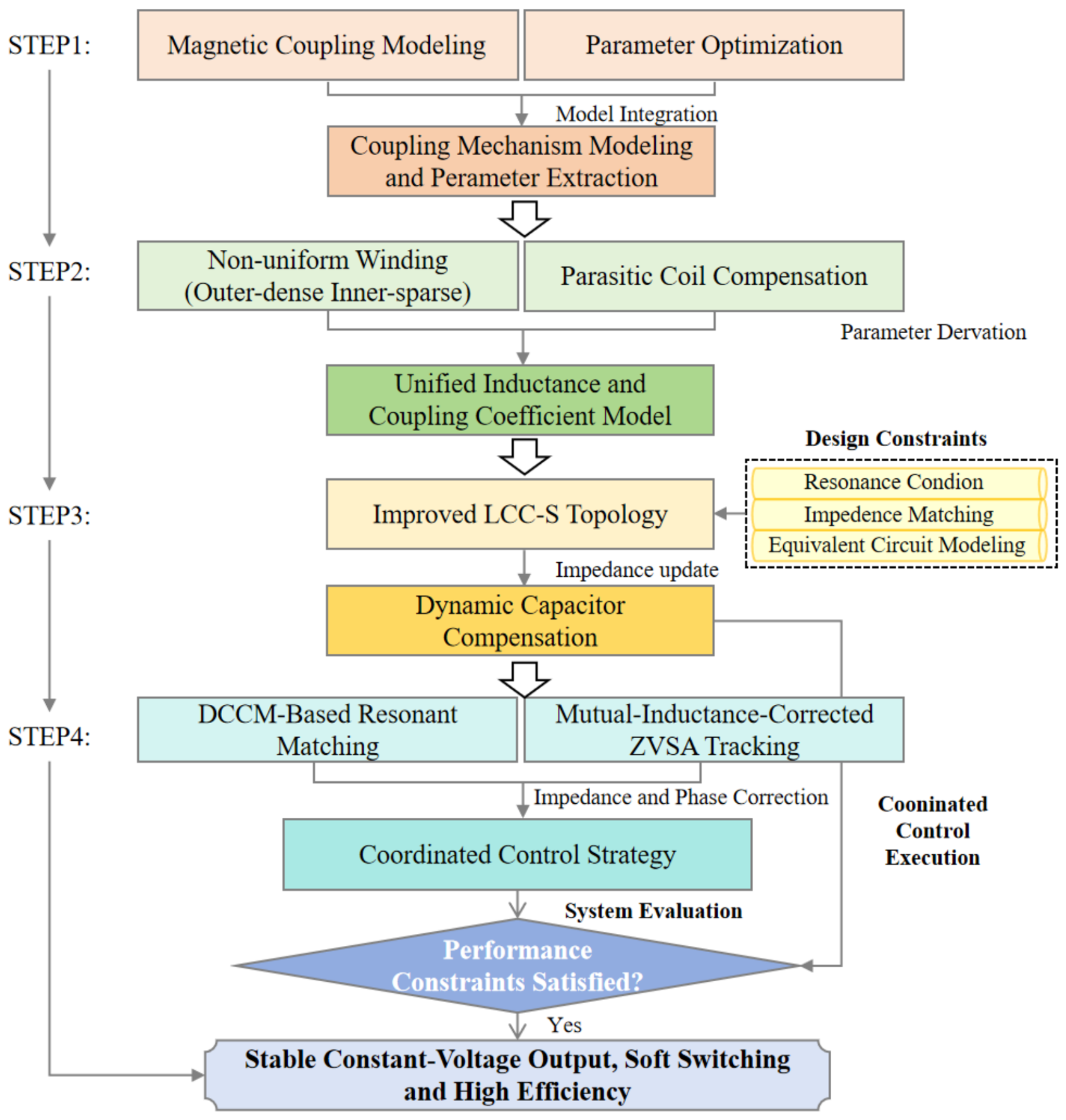
To address these limitations, this paper proposes a dynamically compensated constant-voltage WPT method that combines non-uniform magnetic coupling, parasitic-coil-based passive magnetic-flux compensation, fixed-frequency DCCM-based active impedance matching, and mutual-inductance-corrected ZVSA regulation. Compared with conventional magnetic-coupler optimisation methods, the proposed coupler adopts dense outer windings, loose inner windings, and parasitic coils to enhance effective coupling and regulate leakage flux, and a region-based electromagnetic model is established to characterise the self-inductance, mutual inductance, and coupling coefficient of different winding regions. Compared with fixed resonant-compensation and impedance-regulation methods, an improved LCC-S topology with a dynamic capacitor compensation matrix is developed to adjust the equivalent impedance near the nominal 85 kHz operating frequency, enabling fixed-frequency active impedance matching under load and coupling variations. Compared with conventional frequency, phase, or operating-point control methods, the proposed mutual-inductance-corrected ZVSA tracking method introduces mutual-inductance variation into phase correction, compensates for residual phase deviation, and maintains soft-switching operation while preserving constant-voltage output. The overall implementation is shown in Figure 1.

2. Electromagnetic Modelling of the Proposed Coupling Mechanism

In magnetic inductive WPT systems, the magnetic-coupling parameters of the coupling mechanism directly determine transfer capability, output stability, and energy-transfer efficiency. This section first analyses the magnetic-field distribution and parameter-coupling mechanism of the proposed coupling structure. A region-based electromagnetic model is then established for the densely wound region, loosely wound region, and parasitic coils to characterise self-inductance, mutual inductance, and coupling coefficients. On this basis, an eddy current loss model is further developed to describe the influence of non-uniform magnetic-field distribution on loss characteristics. Finally, the accuracy of the proposed model and the field-regulation effect of the parasitic coils are verified through theoretical comparison and finite-element simulation.

2.1. Region-Based Magnetic Coupling Modelling

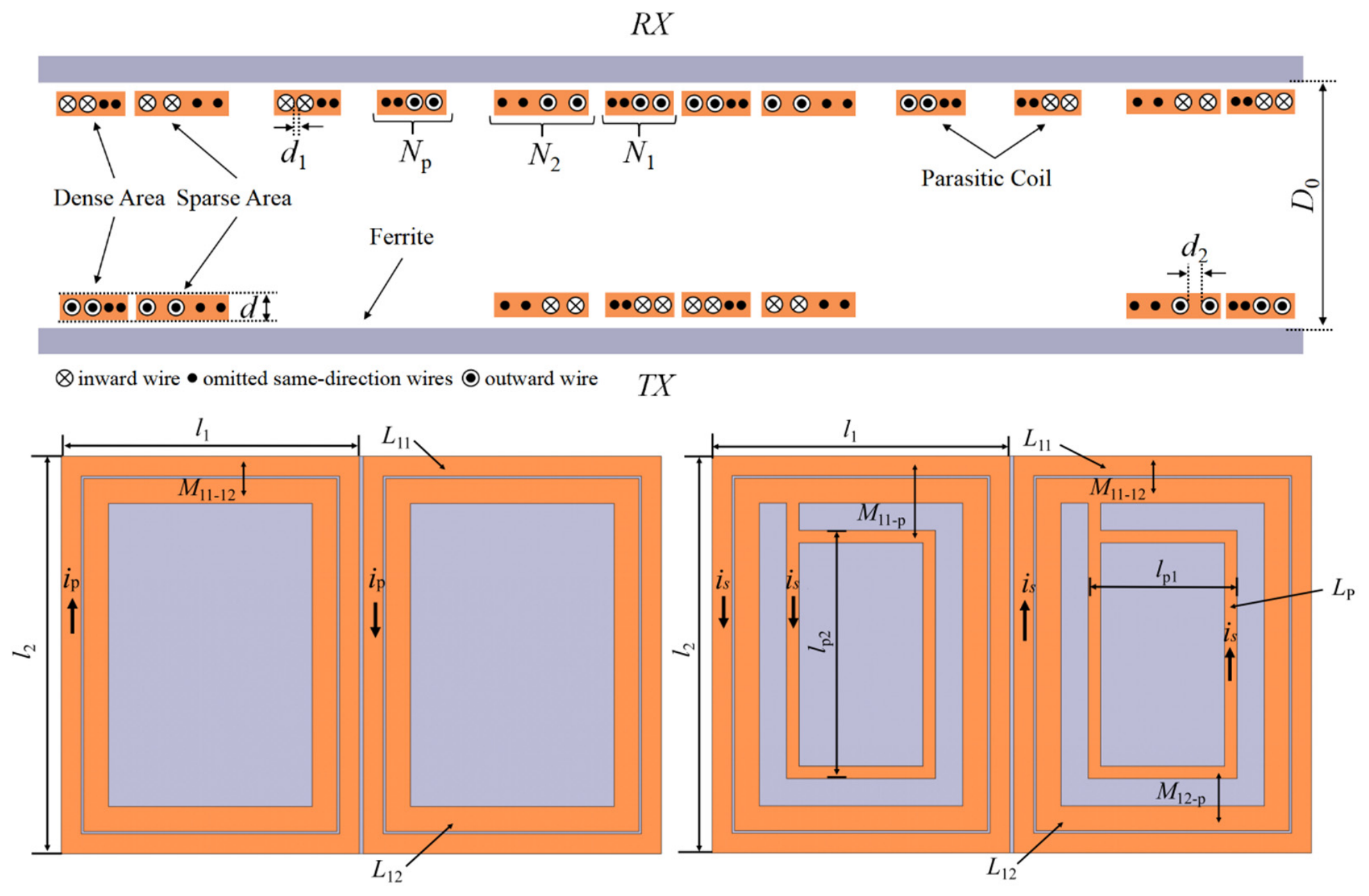
Self-inductance is a key magnetic-coupling parameter affecting system efficiency and output stability. Conventional self-inductance models are usually based on the assumption of uniform windings, making it difficult to describe the magnetic-field differences between densely and loosely wound regions. In addition, the coupling contribution of parasitic coils is often neglected, which may introduce modelling errors. To address this problem, a region-based modelling method derived from the Biot–Savart law is introduced. Equivalent models are established for different winding regions, and the additional coupling contribution of the parasitic coils is incorporated through a correction mechanism. Figure 2 shows the structure of the proposed coupling mechanism and defines the key parameters used in the following derivation. In this work, the densely wound region refers to the winding area with smaller inter-turn spacing and stronger inter-turn coupling, whereas the loosely wound region refers to the winding area with larger inter-turn spacing and weaker inter-turn coupling.
In the densely wound region, inter-turn coupling is strong, and inter-turn mutual inductance cannot be neglected. Therefore, the total magnetic flux consists of both self-flux and mutual flux. Consequently, the self-inductance of the densely wound region L11 is given by
L 11 = ψ 11 I = N 1 2 μ 0 μ r S 1 2 π d + N 1 N 1 1 M 1 . intra
where ψ11 is the total magnetic flux in the densely wound region, N1 is the number of turns in the densely wound region, μ0 is the permeability of free space, μr is the relative permeability of the ferrite core, d is the wire diameter, S1 is the effective area of the primary coil, and M1,intra is the mutual inductance between adjacent turns in the densely wound region.
For the loosely wound region, as the inter-turn coupling is relatively weak, the mutual inductance term has a minor influence on the total magnetic flux. Therefore, the total magnetic flux in this region can be approximated as the self-flux. Taking into account the magnetic field diffusion effect caused by the loose winding structure, a correction factor kloose is introduced to correct the single-turn magnetic flux. Thus, the single-turn loose winding magnetic flux is Φ2,single = klooseΦ1,single, and Φ1,single is the magnetic flux in the single mixed dense winding region. Further, the self-inductance of the main coil’s loosely wound region L12 is obtained as:
L 12 = ψ 12 I = μ 0 μ r N 2 2 S 1 k loose 2 π d
where ψ12 represents the total magnetic flux in the loosely wound region, and N2 represents the number of turns in the loosely wound region.
For the parasitic coil, a tightly wound structure identical to that of the densely wound region is adopted; the effect of inter-turn mutual inductance must also be considered. Similarly, its self-inductance Lp is given by
L p = ψ p I = μ 0 μ r N p 2 S p 2 π d + N p N p 1 M p . intra
where ψp is the total magnetic flux of the parasitic coil, Mp,intra is the mutual inductance between individual turns in the parasitic coil region, Sp is the effective area of the parasitic coil region, and Np is the number of turns in the parasitic coil.
In summary, the total self-inductance of the transmitter and receiver is L1, and L2 is:
L 1 = L 11 + L 12 + 2 M 11 12
L 2 = L 11 + L 12 + L p + 2 M 11 12 + 2 M 11 - p + 2 M 12 - p
where M11-12 is the mutual inductance between the densely wound region and the loosely wound region, M11-p is the mutual inductance between the densely wound region and the parasitic coil, and M12-p is the mutual inductance between the loosely wound region and the parasitic coil.
Based on the established coil self-inductance model, the energy transfer characteristics between the transmitter and receiver coils are further analysed from the perspective of magnetic flux coupling. Under the condition of neglecting the mutual inductance coupling between the parasitic coil and the transmitter/receiver coils, the magnetic field generated by the transmitter coil L1 passes through the main coil of the receiver, At this point, the equivalent self-inductance of the receiving coil, L2,main, comprises only the self-inductance of the densely wound region, L11, and that of the loosely wound region, L12. Under these conditions, the conventional quantitative formula for the coupling system is:
M 0 = ψ 12 , 0 I 1 = N 1 N 2 μ 0 μ r S 2 π d L 1 L 2 , main L 1 L 2 , main = L 1 L 2 , main k 0
where M0 is the mutual inductance between the transmitter and receiver coils when parasitic coils are not considered, ψ12,0 is the total magnetic flux through the main coil of the receiver when parasitic coils are not considered, I1 is the current through the transmitter coil, and k0 is the coupling coefficient in the absence of parasitic coils.
It can be seen from (6) that the traditional mutual inductance model only describes the coupling effect of the main coil flux; in this case, the magnetic flux at the receiving end is primarily contributed by the main magnetic field at the transmitting end, while the compensatory effect of the additional magnetic field from the parasitic coil on the main flux is not taken into account. To address this issue, this paper reconstructs the total magnetic flux at the receiving end and defines the parasitic coil coupling correction coefficient δ [32] to quantify the contribution ratio of the additional magnetic flux:
δ = ψ 21 , p ψ 21 , 0
where ψ21,0 is the main magnetic flux linked with the receiver coil when the parasitic coils are not considered, and ψ21,p is the additional magnetic flux generated by the parasitic coil.
Based on (7), the mutual inductance expression accounting for the effect of the parasitic coil can be further derived as
M = ψ 21 I 1 = M 0 ( 1 + δ )
where ψ21 is the total magnetic flux at the receiving end.
Combining Equations (6)–(8), the following relationship for the coupling coefficient is obtained:
k = ( 1 + δ ) M 0 L 1 L 2
where k denotes the total coupling coefficient accounting for the parasitic coils, and δ characterises the extent to which the parasitic coils contribute to mutual inductance compensation.
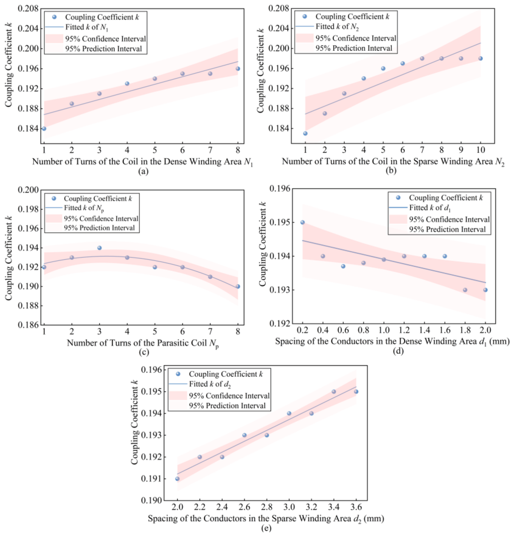
Introducing the parasitic-coupling correction term enables the model to capture both mutual-inductance enhancement and self-inductance variation, thereby improving the description of coupling performance. Based on this model, key structural parameters are optimised at a transmission distance D0 of 200 mm. This distance lies in the moderate-coupling range, avoids extreme operating conditions, and better reflects the influence of structural parameters on coupling characteristics. The results are shown in Figure 3.
As shown in Figure 3, increasing the number of turns in the tightly and loosely wound regions raises the coupling coefficient from approximately 0.184 to 0.196 and from approximately 0.183 to 0.199, respectively, but also increases copper loss. The parasitic coil has an optimum turn number of three turns, and the coupling coefficient peaks at approximately 0.194. For the spacing parameters, reducing the dense-region spacing strengthens local coupling, whereas moderately increasing the loose-region spacing improves the field distribution and coupling capability. Excessive spacing, however, reduces field overlap and limits further improvement. Considering both coupling performance and implementation cost, the selected structural parameters are listed in Table 1.

2.2. Eddy Current Loss Modelling

Eddy current loss is an important factor affecting the loss characteristics of WPT systems. For non-uniform winding structures, the magnetic-field distribution varies significantly among different winding regions, making conventional uniform-field loss models insufficient. To describe this effect, a region-based equivalent loss model is established. For analytical simplicity, the coil conductors are assumed to be circular copper wires, and the system is considered under steady-state sinusoidal excitation. The ferrite core is mainly used for magnetic-flux guidance and leakage-flux suppression. Since high-frequency low-loss Mn–Zn ferrite is adopted in the prototype and the ferrite-core loss accounts for less than 1.5% of the overall system efficiency under the tested operating conditions, ferrite loss is treated as a secondary loss term in the analytical model. The magnetic field in each winding region is calculated independently, while the coupling effect between regions is represented by flux superposition. Higher-order coupling terms are neglected. The average eddy current loss in a single-turn conductor Peddy,single can be expressed as
P eddy , single = π σ ω 2 B m 2 r D 4 l 16
where σ is the electrical conductivity of the copper conductor, ω = 2πf is the operating angular frequency, Bm represents the magnitude of the magnetic flux density in a single-turn coil, rD represents the radius of the conductor, and l represents the length of the single-turn coil.
At the nominal operating frequency of 85 kHz, skin effect and proximity effect are further considered by introducing high-frequency correction coefficients. The skin-effect correction coefficient is set as kskin = 1.2. The proximity-effect correction coefficients are set as kprox,1 = 1.1 for the densely wound region, kprox,2 = 1.0 for the loosely wound region, and kprox,p = 1.1 for the parasitic coil.
Building on this, to account for differences in magnetic field distribution caused by different winding structures, a regional correction mechanism is introduced. For densely wound regions, due to the small inter-turn spacing, the local magnetic flux density increases, leading to an increase in eddy current losses; this is corrected by the dense winding correction coefficient kdense. For loosely wound regions, due to the large inter-turn spacing, the magnetic field distribution tends to be uniform, and the eddy current effect is relatively weakened. Its characteristics are described by the loose winding correction coefficient kloose described in Section 2.1. The parasitic coil adopts a densely wound structure and achieves leakage flux compensation by modulating the main flux path. To quantify this effect, the parasitic coupling correction coefficient δ described in Section 2.1 is introduced. Further consideration is given to the magnetic field coupling between regions; in this case, the additional losses caused by coupling are described by the overall coupling correction factor ΔPeddy for residual coupling. The total eddy current loss of the system Peddy,tot can then be expressed as
P eddy , tot = k skin π σ ω 2 r D 4 16 ( N 1 k dense k prox , 1 B m 1 2 l 1 + N 2 k loose k prox , 2 B m 2 2 l 2 + N p k dense k prox , p δ 2 B mp 2 l p ) + Δ P eddy
where Bm1 is the average magnetic flux density of a single-turn coil in the densely wound region, l1 is the outer contour length of the densely wound region, Bm2 is the average magnetic flux density of a single-turn coil in the loosely wound region, l2 is the outer contour length of the loosely wound region, Bmp is the average magnetic flux density of a single-turn coil in the parasitic coil, and lp is the outer contour length of the parasitic coil.
This expression extends the single-turn loss model to a multi-region coupled structure and describes the modulation effect of the non-uniform winding pattern on eddy current loss distribution. The densely wound region is associated with stronger local magnetic flux density and higher potential eddy current loss, whereas the loosely wound region reduces field concentration owing to its larger inter-turn spacing. The parasitic coils further reshape the main flux path and suppress edge leakage, thereby improving the uniformity of the magnetic-field distribution. The validity of this modelling result is further examined in Section 2.3 through finite-element field simulation.

2.3. Verification of the Electromagnetic Model

Before the proposed model is used for topology design and performance analysis, its accuracy must be verified. Therefore, this section validates the model from two aspects: first, self-inductance, mutual inductance, and coupling coefficient are compared with those of the conventional model; second, the magnetic flux density distribution is analysed by finite-element simulation to verify the field-regulation effect of the parasitic coils.
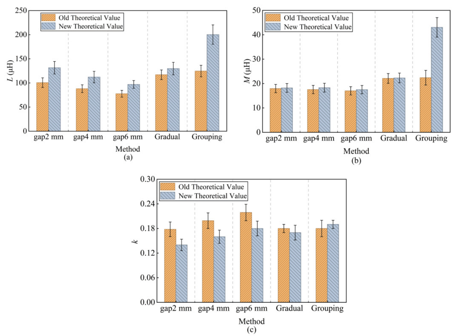
Using the structural parameters listed in Table 1, the conventional and proposed models are compared under different winding structures to verify the accuracy of the region-based electromagnetic parameter model, as shown in Figure 4.
The self-inductance results show that the proposed model gives higher values than the conventional model for all structures: approximately 20–30% higher for uniform windings, approximately 11% higher for progressive windings, and more than 40% higher after parasitic coils are introduced. This confirms that the model captures flux superposition and compensation effects. The mutual-inductance comparison shows that the two models are largely consistent except for the grouping structure. After the parasitic coil is introduced, the mutual inductance increases from approximately 31 μH to approximately 43 μH, indicating that the additional parasitic-coil flux enhances coupling. The coupling-coefficient results are generally lower than those of the conventional model because the conventional self-inductance calculation introduces a relatively large error. In the grouping structure, however, the parasitic coil increases the coupling coefficient to approximately 0.20 because mutual-inductance enhancement dominates. Overall, the proposed model corrects the conventional model error and reveals the flux-compensation and coupling-enhancement effects of the parasitic coil.
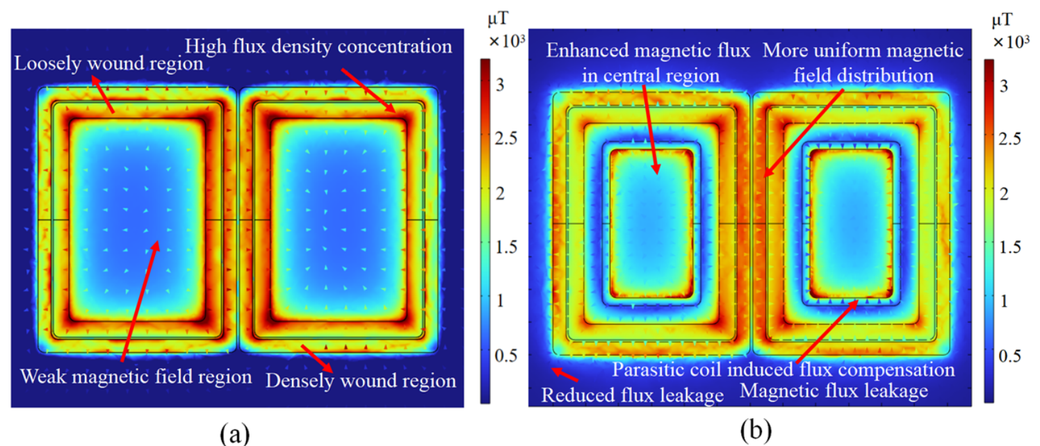
To further verify the magnetic-field regulation effect predicted by the eddy current loss model, a finite-element simulation was conducted in COMSOL Multiphysics 6.3 using the structural parameters listed in Table 1. The electrical conductivity of copper was set to 5.8 × 10⁷ S/m, and the relative permeability of the ferrite core was set to 2000 to represent the flux-confinement capability of typical power ferrite materials under medium-frequency operation. Since the equivalent model does not directly provide eddy current loss density, the magnetic flux density distribution was used as an indirect indicator of the loss distribution. A 1 A excitation current was applied to the transmitting and receiving coils, and the magnetic flux density distribution in the xy plane was extracted, as shown in Figure 5.
Figure 5 shows that the magnetic flux density is mainly concentrated in the densely wound region, where the peak value reaches approximately 2.5–3.0 × 10³ μT. This value is significantly higher than the 0.5–1.0 × 10³ μT observed in the central region, indicating typical local flux concentration. Since eddy current loss is closely related to magnetic-field strength, the densely wound region corresponds to a higher potential loss level, whereas the loosely wound region exhibits a lower loss tendency owing to its weaker field concentration. After the parasitic coils are introduced, the central magnetic flux is enhanced, edge leakage is suppressed, and the overall field distribution becomes more uniform. These results are consistent with the region-based loss model and further confirm the effectiveness of the proposed electromagnetic model.

3. Dynamic Compensation Topology and Control Strategy

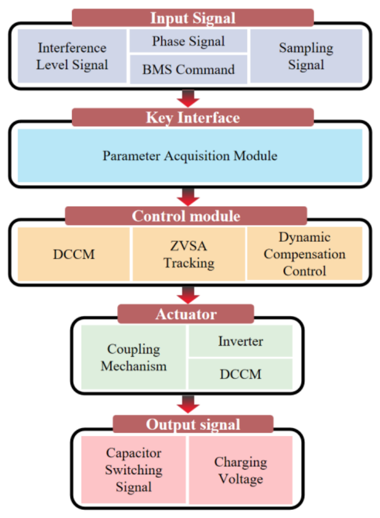
In WPT systems, performance depends on the coordinated design of the compensation topology and control strategy. To maintain constant-voltage output and soft-switching operation under load and coupling-parameter variations, this section develops a coordinated strategy that combines dynamic compensation capacitance and zero-voltage-switching angle (ZVSA) tracking within an improved LCC-S topology. The overall process is shown in Figure 6. The dynamic compensation capacitance is used to restore resonant matching, while ZVSA tracking is used to correct phase deviation and maintain efficient soft-switching operation.

3.1. Improved LCC-S Compensation Network and Operating Principle

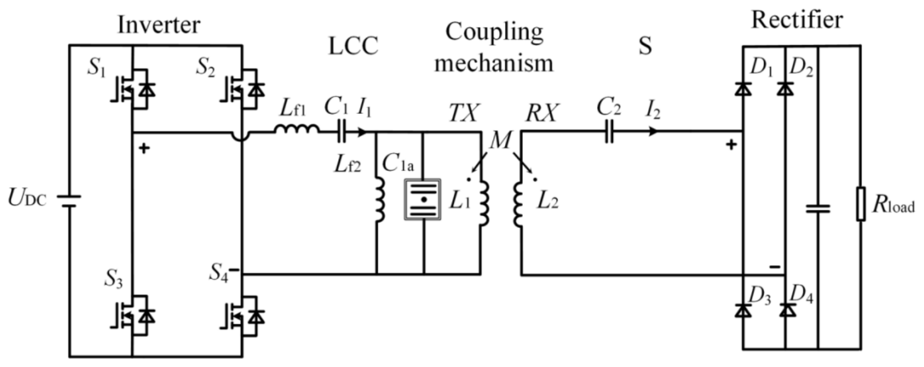
This section introduces a dynamic compensation capacitor into the conventional LCC-S topology to improve resonant matching under load variation and coil offset, thereby enabling stable constant-voltage output over a wide operating range. The system structure is shown in Figure 7. The system comprises a full-bridge inverter, a transmitter-side LCC network, a magnetic coupling mechanism, and a receiver-side S-compensation and rectification circuit. By adjusting the equivalent impedance at the transmitter end, adaptive matching of the resonance conditions is achieved, enabling the system to operate stably near the target frequency.
In the theoretical analysis, the rectifier adopts an ideal full-bridge model, and the output filter capacitance is sufficiently large, resulting in a low output voltage ripple that can be approximated as constant. Under the First Harmonic Approximation (FHA), the fundamental voltage of the inverter output Uab,1, and the equivalent load on the rectifier side Rac can be expressed as
U ab , 1 = 2 2 π U DC
where UDC is the input DC voltage.
R ac = 8 π 2 R load
where Rload is the system load.
The receiving side consists of a series resonant circuit formed by a coil and a compensation capacitor, whose equivalent impedance Z2 is given by:
Z 2 = r 2 + R ac + j ω L 2 1 ω C 2
where L2 is the inductance of the receiving coil, C2 is the compensation capacitor on the receiving side, and r2 is the parasitic resistance on the receiving side.
From this, the series resonance condition for the secondary side is obtained:
C 2 = 1 ω 2 L 2
Based on the mutual inductance coupling relationship, the secondary-side impedance can be equated to the primary-side reflection impedance Zref, thereby yielding the equivalent impedance of the transmitter coil branch Z1,br:
Z ref = ( ω M ) 2 Z 2
Z 1 , br = r 1 + j ω L 1 + Z ref
where L1 is the inductance of the transmit coil, and r1 is the parasitic resistance on the transmit side.
For the primary side, a parallel network is formed by the parallel compensation inductance Lf2, the dynamic capacitance C1a, and the transmit coil L1. Its resonance condition can be determined by setting the imaginary part of the admittance to zero, so the parallel resonance relationship is:
C 1 a = 1 ω 2 L f 2 1 ω Im 1 Z 1 , br
Meanwhile, the series resonant branch on the input side satisfies:
C 1 = 1 ω 2 L f 1
where Lf1 is the primary-side series compensation inductance, and C1 is the primary-side series compensation capacitance.
When all three resonance conditions are satisfied simultaneously, the equivalent system model is simplified, and the output voltage Uo can be expressed as
U o = ω M U DC ( ω M ) 2 R ac 2 + ( ω L 1 ) 2
when ( ω M ) 2 / R ac ω L 1 is satisfied, the above equation can be expressed as
U o M L 1 U DC
where (21) shows that the output voltage is mainly determined by the input voltage and coil parameters, which are insensitive to load variation and exhibit a constant-voltage characteristic.

3.2. Modelling and Derivation of the Dynamic Capacitance Compensation Matrix

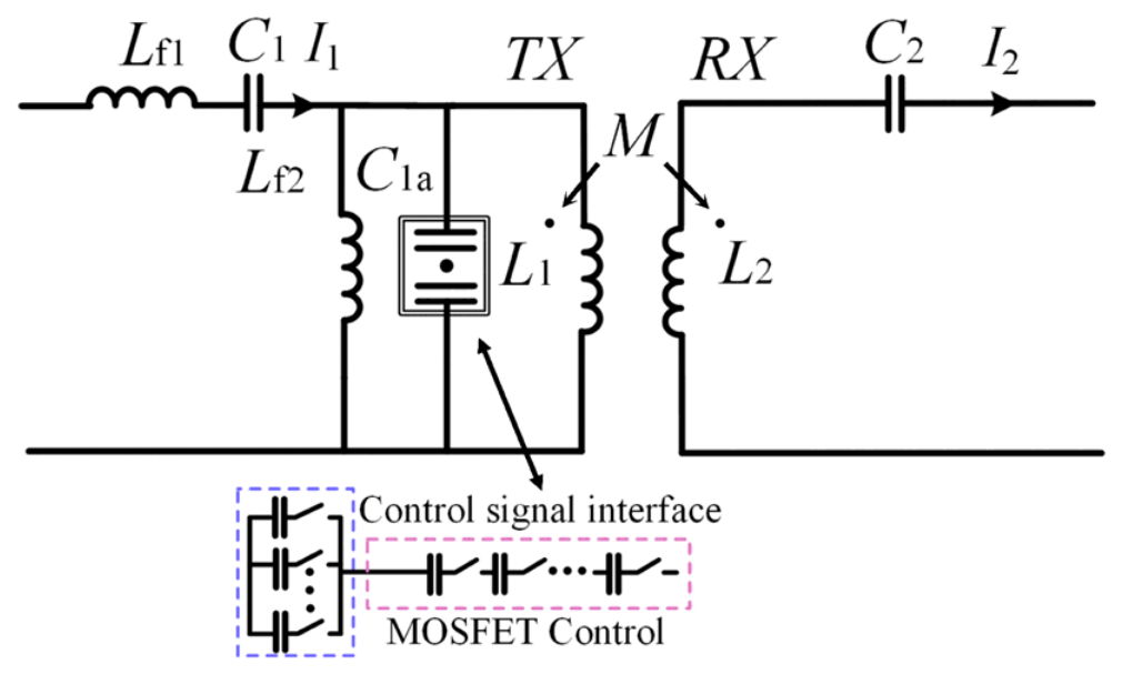
Under practical operating conditions, load variation and coil displacement change the system equivalent impedance, causing the natural resonant frequency to deviate from the target operating frequency of 85 kHz. To achieve rapid dynamic impedance matching, this section constructs a dynamic capacitance compensation matrix (DCCM), as shown in Figure 8. By adjusting the compensation capacitance, the DCCM adaptively tracks the resonant frequency and maintains stable, efficient operation.
From Equations (14) and (16), it can be seen that the secondary side exhibits a purely resistive behaviour during series resonance, and its equivalent impedance Zf reflected back to the primary side is given by:
Z f = ( ω 0 M ) 2 r 2 + R ac
The natural resonant frequency of the system is determined jointly by the equivalent inductance and the equivalent capacitance, and is expressed as
ω 0 = 1 L eq C eq
where Leq is the total equivalent inductance at the transmitter end, and Ceq is the total equivalent compensation capacitance at the transmitter end, where Leq = f(L1,Lf1,Lf2,M), and Ceq = f(C1,C1a).
Taking the modified equivalent impedance as the target impedance Ztarget, the expression for the dynamic compensation capacitance is obtained as
C 1 a , target = 1 ω 0 2 L f 2 + L 1 Z target 2 + ( ω 0 L 1 ) 2
It can be seen from Equation (24) that changes in the load resistance and mutual inductance will cause a shift in the equivalent impedance through the reflected impedance, thereby leading to a drift in the resonant condition. To maintain stable operation at the target frequency, the compensation capacitance must be dynamically adjusted. While load variation can be directly characterised by the circuit model, the mutual-inductance variation caused by coil displacement requires an additional attenuation description. Therefore, a displacement attenuation coefficient kΔ is introduced to model the dynamic mutual inductance. In this work, kΔ is obtained from a three-dimensional electromagnetic-field coupling simulation in COMSOL and fitted according to a Gaussian attenuation relationship.
M = M t 1 k Δ Δ , Δ = Δ x 2 + Δ y 2
k Δ = exp ( Δ 2 2 τ 2 )
where Mt is the mutual inductance when the coupling mechanism is aligned, Δ is the total offset, and τ is the characteristic attenuation length in cm, which is fitted from the COMSOL simulation and measured mutual-inductance data within 0–5 cm with an error of less than 3%.
Solving Equations (17), (18), (22) and (25) simultaneously yields the following expression for the target impedance:
Z target = r 1 + ω 0 2 M t 2 ( 1 k Δ Δ ) 2 r 2 + 8 π 2 R load
From this, the complete expression for the dynamic capacitance C1a,opt(Rload,Δ) is obtained as
C 1 a , opt ( R load , Δ ) = 1 ω 0 2 L f 2 + L 1 r 1 + ω 0 2 M t 2 ( 1 k Δ Δ ) 2 r 2 + 8 π 2 R load 2 + ( ω 0 L 1 ) 2
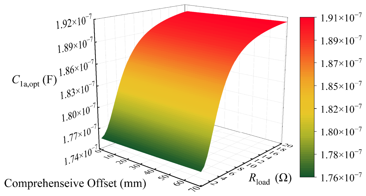
To illustrate the response characteristics of the dynamic compensation capacitor to load variations and the total offset, this paper conducts a multi-parameter analysis of the optimal compensation capacitor C1a,opt, the results of which are shown in Figure 9.
As shown in Figure 9, the compensation capacitance varies smoothly with load and offset. The DCCM can therefore compensate for resonance drift caused by load variation and coil displacement, confirming the adaptive capability of the proposed method.
In the prototype, the DCCM is realised by an 8-bit binary-weighted film-capacitor array with a basic unit of 0.5 nF, providing 256 selectable capacitance levels within 170–230 nF and a minimum resolution of 0.5 nF. Low-voltage Si MOSFETs are used as branch-selection switches, with a turn-on delay of less than 1μs, and the control sampling frequency is set to 10 kHz to satisfy the millisecond-level dynamic response requirement. To suppress output-voltage jitter caused by discrete capacitance switching, a threshold-based update strategy is adopted: capacitance adjustment is triggered only when the output-voltage deviation exceeds 1% of the rated value or when the calculated optimal capacitance changes by more than one step. Small voltage fluctuations are absorbed by the inherent impedance-buffering characteristic of the resonant network without immediate switching. Under the present hardware conditions, the measured voltage ripple caused by DCCM quantisation and switching is limited to approximately ±0.2 V. In future work, the array will be extended from 8 bits to 10 bits to reduce single-step capacitance tolerance and further suppress voltage jumps. Owing to the use of low-ESR film capacitors and low-resistance MOSFET paths, the additional DCCM loss is estimated to be less than 1% of the rated output power, indicating a minor influence on the overall efficiency.

3.3. Precise Tracking Algorithm for Zero-Voltage Switching Angle

ZVSA control enables the switching devices to turn on under near-zero-voltage conditions, thereby reducing switching loss and improving system efficiency. However, coil misalignment changes the mutual inductance and reflected impedance, which may introduce phase deviation and move the converter away from the desired soft-switching region. To address this issue, a mutual-inductance correction mechanism is introduced to construct a ZVSA tracking model under coupling variation.
Based on the Voltage-Fed Phase-Shift Switching (VF-PSC) control strategy for the, the fundamental component of the inverter output voltage, uin1, is given by:
u in 1 = 2 2 π U DC sin D π 2 sin ω t + φ u
In the equation, D represents the inverter duty cycle, and φu represents the voltage phase.
At this point, the transmitter resonant current is iL1:
i L 1 = I L 1 m sin ω t + φ i
where IL1,m is the amplitude of the transmitter resonant current, and φi is the phase of the transmitter resonant current.
At the moment the switching transistor turns on, the condition φi < φu must be satisfied; hence, the phase angle φZVSA of ZVSA is defined as
φ ZVSA = φ u φ i
Taking into account both switching losses and dynamic response characteristics, this paper selects a reference ZVSA phase angle φZVSA,ref of 30°. Under coupling-parameter variations, the mutual inductance changes the reflected impedance and further affects the phase of the resonant current. According to Equations (14), (16) and (17), the equivalent impedance of the transmitter coil branch, Z1,br, can be regarded as a function of the mutual inductance M. Therefore, considering the primary-side series and parallel compensation branches, the input impedance of the compensation network is denoted as Zin(M) and expressed as
Z in ( M ) = j ω L f 1 + 1 j ω C 1 + 1 j ω L f 2 + j ω C 1 a + 1 Z 1 , br ( M ) 1
Since the phase of the resonant current is determined by the phase angle of the input impedance, the phase correction caused by mutual-inductance variation is defined as ΔφM:
Δ φ M = arg Z in ( M ) + arg Z in ( M t )
where Mt is the mutual inductance under the aligned coupling condition, as defined in Equation (25).
Based on this correction term, the corrected ZVSA phase is denoted as φZVSA:
φ ZVSA = φ ZVSA + Δ φ M
The ZVSA tracking objective is then set by forcing the corrected phase φZVSA to approach the reference value φZVSA,ref. On this basis, closed-loop control is achieved by adjusting the inverter switching angular frequency, and a proportional–integral control mechanism is used to dynamically compensate for the phase error. The frequency adjustment is denoted as Δω and expressed as
Δ ω = K p φ ZVSA , ref φ ZVSA + K i φ ZVSA , ref φ ZVSA d t ω 0
where Kp and Ki are the proportional and integral control parameters, respectively.
To further clarify the controller parameter selection, stability, and convergence characteristics, the ZVSA tracking loop is analysed around the nominal operating point. In this work, Kp is mainly used to improve the transient correction speed, while Ki is used to eliminate the steady-state phase error. To avoid excessive switching-frequency deviation, the frequency adjustment Δω is limited within a small range around the nominal angular frequency ω0.
Around the nominal operating point, the relationship between the ZVSA and the switching angular frequency can be locally linearised as ΔφZVSASωΔω, where S ω = φ ZVSA / ω is the local phase-frequency sensitivity. Since the system operates near the soft-switching region, Sω remains bounded within the considered operating range. Therefore, the closed-loop ZVSA tracking process is locally stable when the controller gains are selected to satisfy SωKp > 0 and SωKi > 0. In practical tuning, Kp and Ki are selected to obtain a fast phase recovery while avoiding excessive overshoot or oscillation.
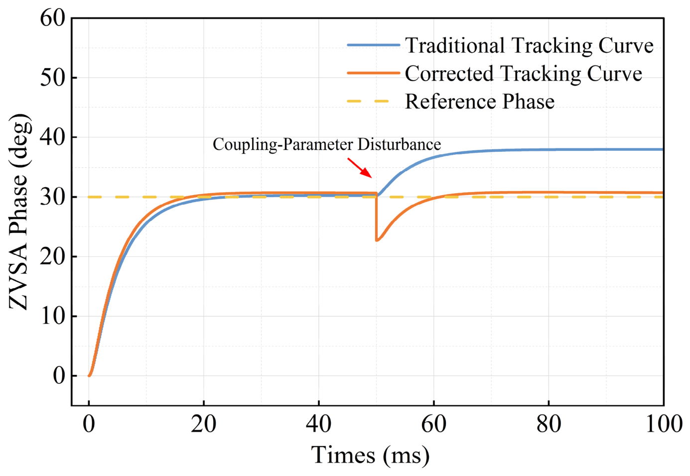
To improve robustness against measurement noise, the measured voltage and current phases are averaged over several switching cycles before calculating φZVSA. In addition, Δω is limited to suppress abrupt frequency correction caused by high-frequency phase noise. This treatment reduces random phase fluctuation while preserving the response to low-frequency coupling-parameter variations. The convergence behaviour of the proposed tracking method is further verified by the dynamic disturbance results shown in Figure 10.
Figure 10 shows that coupling-parameter variation causes the conventional tracking curve to deviate markedly: the ZVSA phase shifts from the 30° reference to approximately 38°. By contrast, the proposed method rapidly corrects the phase towards the reference, with only a transient undershoot to approximately 25° and recovery to 30° within about 10 ms. The results indicate that the proposed mutual-inductance-corrected ZVSA tracking method can effectively compensate for phase deviation caused by coupling-parameter variation and support stable soft-switching operation.

4. Simulation Verification

To evaluate the theoretical analysis and control strategy of the proposed WPT system, a MATLAB R2024a-based simulation model was constructed using the parameters listed in Table 2. Constant-voltage output, parameter sensitivity, dynamic response, and robustness were then analysed.

4.1. Constant Voltage Characteristics and Load Performance

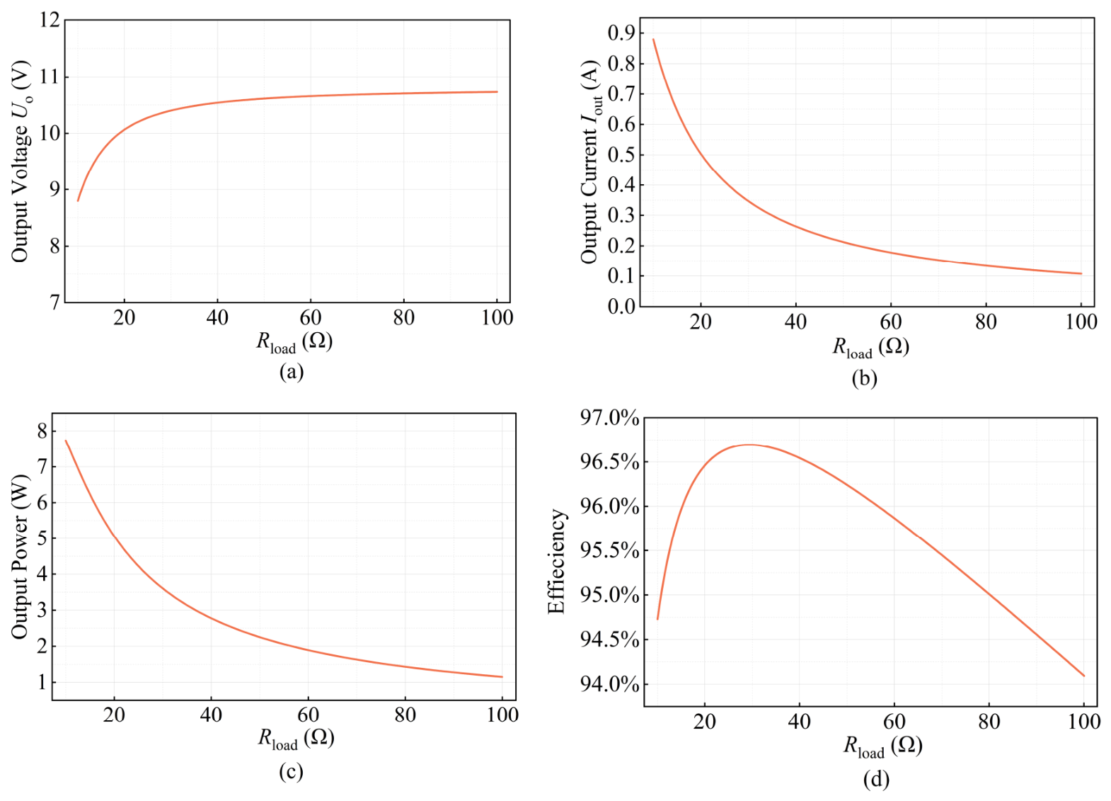
To evaluate output stability and control performance under load variation, this section analyses the steady-state and dynamic output behaviour. Figure 11 shows the output characteristics over a wide load range and is used to assess voltage stability and transfer performance under different load conditions.
Figure 11 shows that when the load exceeds 20 Ω, the output voltage remains close to the rated value with only small fluctuations, demonstrating constant-voltage capability. As the load decreases, the output current increases, and the output power rises accordingly, which is consistent with resistive-load behaviour and further confirms that the output voltage is nearly constant. The efficiency remains above 90% in the main operating range, indicating that the proposed compensation topology combines voltage stability with efficient power transfer.
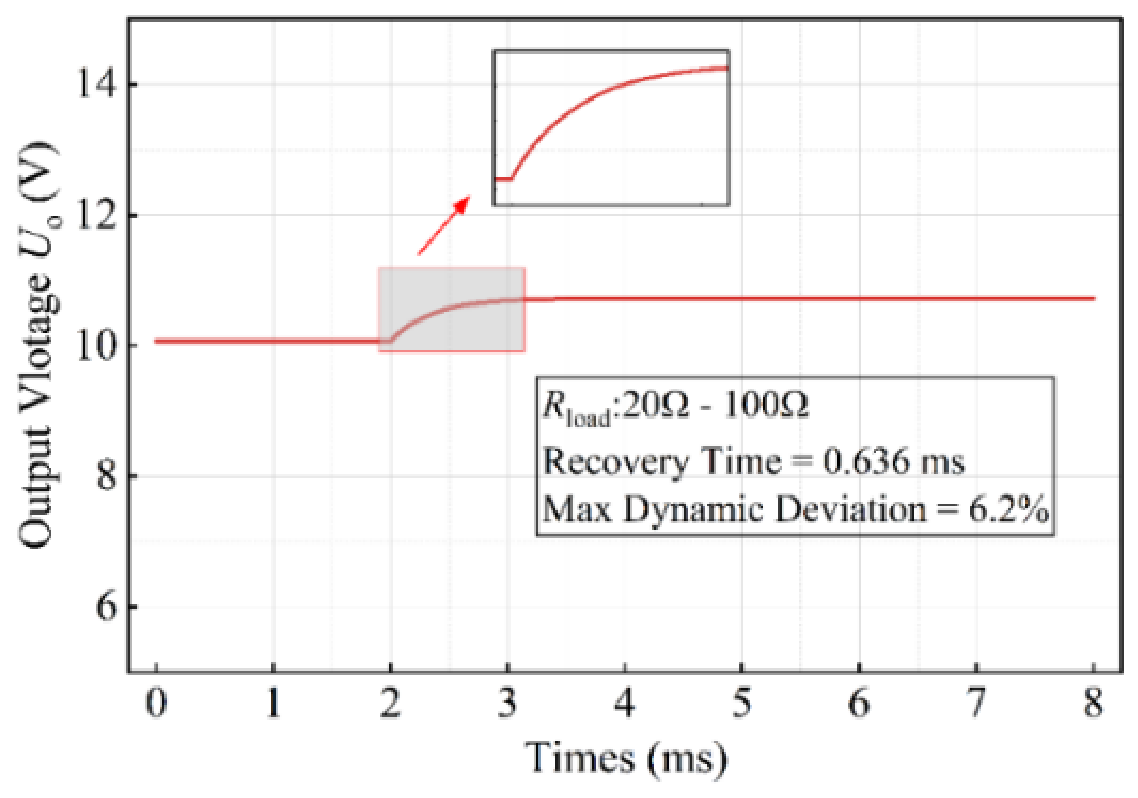
To further evaluate the response to sudden load variation, a load-step scenario was simulated, as shown in Figure 12. When the load changes abruptly from 20 Ω to 100 Ω, the output voltage briefly rises from 10 V, reaches a maximum dynamic deviation of approximately 6.2%, and returns to a steady-state value of approximately 10.7 V within about 0.636 ms. The system, therefore, shows only minor transient fluctuations under load steps and recovers rapidly, validating its dynamic regulation capability. These results verify that the improved LCC-S topology can maintain stable, constant-voltage output across a wide load range and under dynamic load changes.

4.2. Parameter Sensitivity Analysis and System Robustness

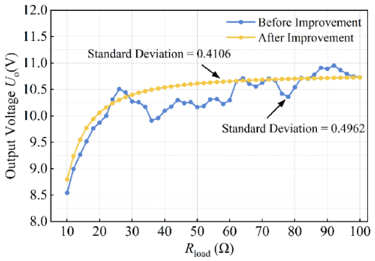
To assess robustness under non-ideal conditions, this section analyses the sensitivity of the output voltage to compensation parameters, mutual inductance, and operating frequency. Figure 13 shows the output-voltage variation when the primary-side series compensation inductance Lf1 and parallel compensation inductance Lf2 deviate from their nominal values, thereby revealing the influence of compensation-parameter deviation on output stability.
As shown in Figure 13, as the compensation parameters deviate from their design values, fluctuations in the output voltage increase significantly, indicating that the system’s resonant state is affected. Using the standard deviation of the output voltage as an evaluation metric, it can be seen that voltage fluctuations are minimal when L f 1 = 30 μH and L f 2 = 20 μH; the standard deviation decreases from 0.4962 before optimisation to 0.4106, with the system being closest to the ideal resonant state.
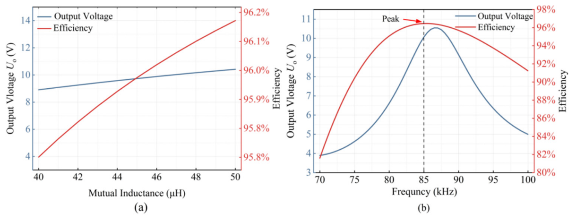
Figure 14 shows the system response under variations in mutual inductance and operating frequency, including their effects on output characteristics and transfer efficiency. Within the analysed range, the output voltage remains close to the target value, and the transfer efficiency does not drop significantly, indicating good robustness to coupling variation. Around 85 kHz, both output voltage and efficiency remain near their optimal values, and the output is stable under moderate parameter deviation.
In summary, the proposed method shows robustness to compensation parameters, mutual inductance, and operating frequency deviations. Dynamic adjustment maintains resonance matching and therefore supports stable voltage output and efficient energy transfer.

4.3. Comprehensive Efficiency Analysis

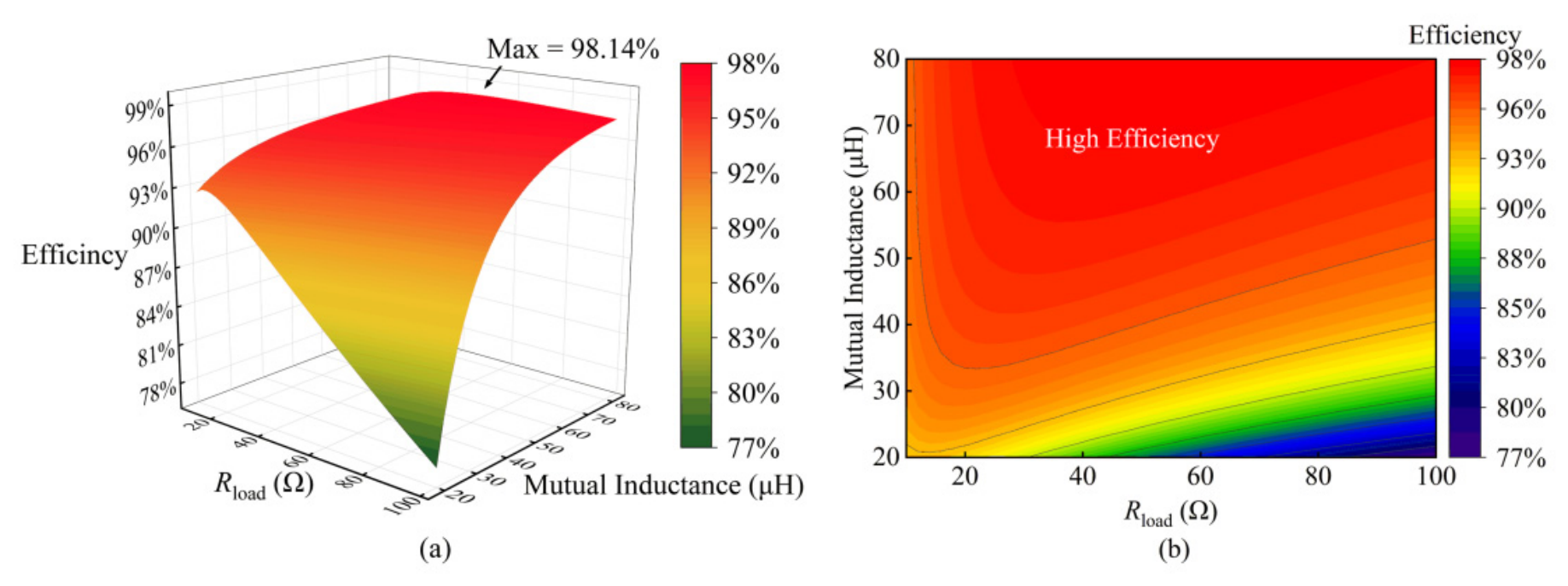
To further evaluate energy-transfer performance and model accuracy under different operating conditions, this section analyses the efficiency distribution and output-voltage consistency. Figure 15 shows the influence of load and mutual inductance on transfer efficiency.
Figure 15 shows that the system maintains high efficiency over a wide parameter range, with high-efficiency regions appearing at moderate load and high mutual inductance. Under the optimal parameter combination and in the loss-neglected simulation, the maximum efficiency reaches 98.14%. This value should be interpreted as an idealised simulation result rather than a directly measured efficiency.
The peak efficiency of 98.14% in Figure 15 is an idealised simulation result mainly considering coil copper loss; after semiconductor switching loss, semiconductor conduction loss, compensation-capacitor ESR loss, ferrite-core loss, and rectifier conduction loss are included, the maximum simulated efficiency decreases to 94.4%, which is reasonably close to the measured peak efficiency of 93.7%.
To further identify the dominant loss mechanisms, a full-loss simulation was conducted under the nominal aligned condition and the 5 cm offset condition. Under the nominal aligned condition, coil copper loss, inverter switching loss, rectifier conduction loss, compensation-capacitor ESR loss, ferrite-core loss, and DCCM-related loss account for approximately 38.6%, 26.8%, 15.7%, 8.4%, 5.1%, and 5.4% of the total loss, respectively. Under the 5 cm offset condition, the proportions of coil copper loss and inverter switching loss increase to approximately 41.3% and 29.6%, respectively, due to weakened coupling, increased circulating current, and larger phase deviation. Therefore, coil copper loss and inverter switching loss are the dominant loss sources of the proposed system.
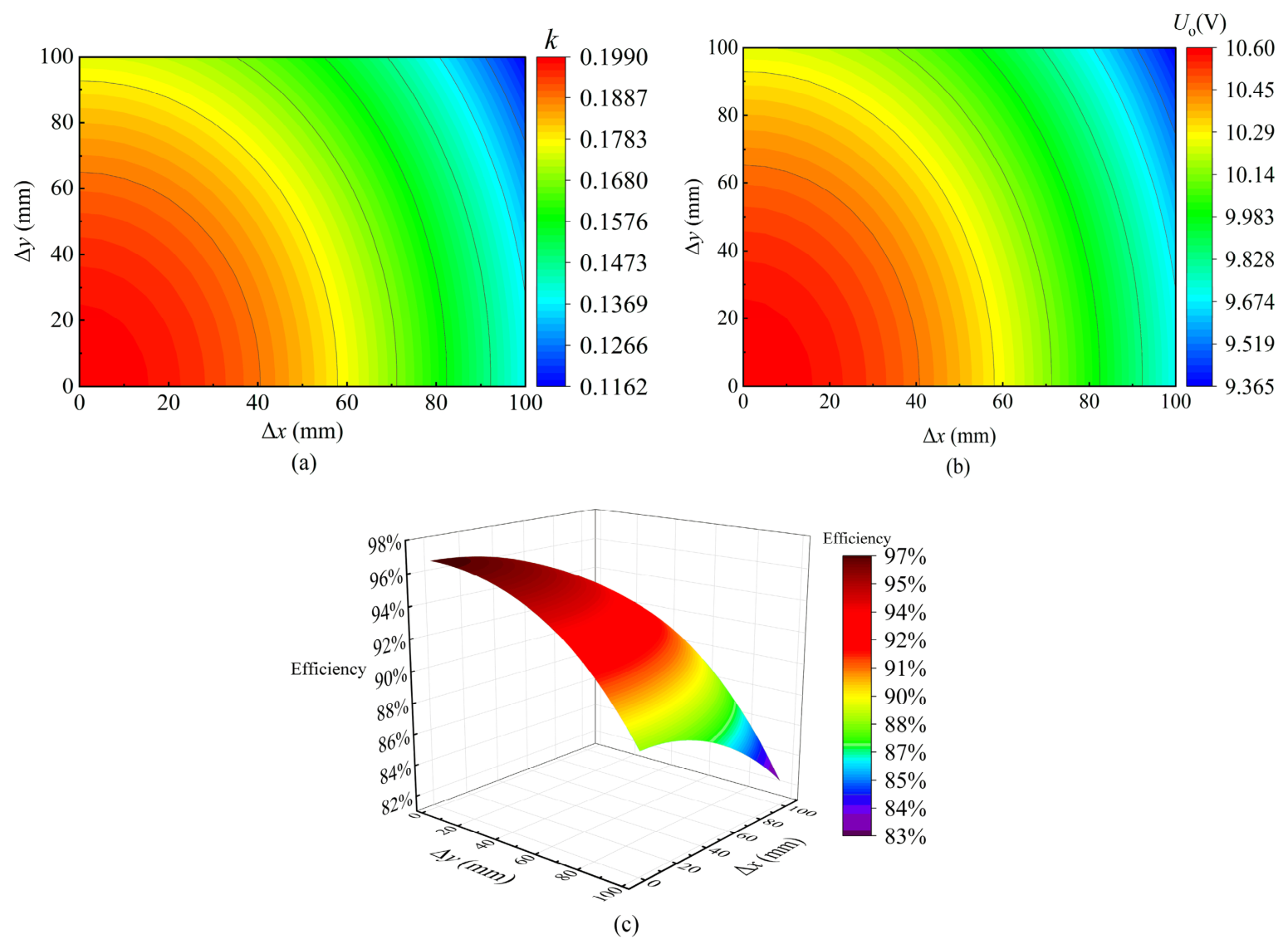
In addition, the misalignment tolerance was evaluated by extending the lateral and longitudinal offset range to 0–10 cm in simulation while keeping the input voltage, load resistance, and operating frequency unchanged. The corresponding coupling coefficient, output voltage, and efficiency distributions are shown in Figure 16.
As shown in Figure 16, the coupling coefficient, output voltage, and efficiency all decrease with increasing lateral and longitudinal offsets, and the degradation becomes more obvious under simultaneous two-direction misalignment. Nevertheless, the output voltage remains relatively stable within the simulated 0–10 cm offset range, indicating that the proposed DCCM and ZVSA strategy can improve voltage-regulation robustness under coupling variation. It should be noted that the efficiency map is an estimated simulation result, and some practical device losses are not fully included.

5. Experimental Verification

The experimental verification focuses on the dynamic compensation mechanism and its ability to maintain constant-voltage output under load variation and coil offset. A single-coupling WPT prototype was constructed to validate the core compensation principle and practical transfer performance of the proposed method. The prototype is intended as a proof-of-principle platform rather than a direct high-power industrial implementation. Due to the limited travel range of the experimental guide rail, the physical offset tests in this section were conducted only within 5 cm, while the extended 0–10 cm offset range was evaluated by simulation in Section 4.

5.1. Experimental Platform Setup

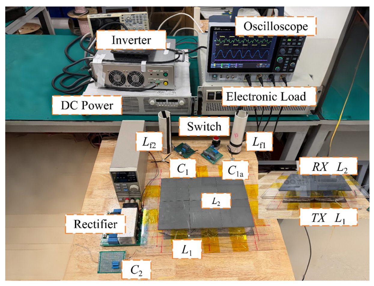
To verify the practical effectiveness of the dynamic compensation capacitor, a WPT experimental platform was constructed. Considering manufacturing constraints and component cost, a scaled prototype was built using a similarity method. The experimental coupler was reduced to half of the simulated geometric size while keeping the winding structure and materials unchanged. Therefore, the inductance and mutual inductance approximately scale with the geometric size. The theoretical scaled values of L1, L2, and M are 96.54 μH, 121.46 μH, and 21.52 μH, while the measured values are 94.8 μH, 116 μH, and 21 μH, respectively. The deviations mainly come from manual winding tolerance and ferrite assembly gaps. The operating frequency remained 85 kHz, and the compensation capacitors were recalculated based on the measured inductances.
The overall structure of the experimental platform is shown in Figure 17. It primarily consists of a DC power supply, a full-bridge inverter, a transmitter-side compensation network, a magnetic coupling mechanism, a receiver-side compensation network, a rectifier circuit, and an electronic load. Detailed system specifications and parameters are given in Table 3. During the experiment, considering that the system operates at a switching frequency of 85 kHz, the coupling coil was wound using 150 strands of Litz wire to avoid a significant increase in AC resistance. The compensation capacitance is formed by a parallel combination of multiple film capacitors, with the dynamic compensation capacitance C1a adjusted via a switching array. The inverter employs SiC MOSFETs, the rectifier uses SiC diodes, and a digital controller is used to generate the PWM drive signal. All efficiency tests were repeated five times under each operating condition, and the average values were used. The voltage and current accuracies of the DC power supply were ±0.1% and ±0.2%, respectively. The voltage and current accuracies of the electronic load were ±0.05% and ±0.1%, respectively. The oscilloscope voltage measurement accuracy was ±2%. Considering instrument precision and repeatability, the combined uncertainty of the system efficiency was estimated to be within ±0.4 percentage points.

5.2. Verification of Constant Voltage Characteristics Under Different Operating Conditions

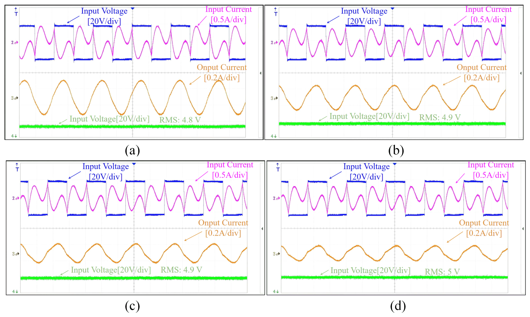
Based on the experimental platform constructed, tests were conducted on the constant-voltage output characteristics under varying load and coil offset conditions. Figure 18 shows the experimental waveforms under different loads to verify the system’s output characteristics and stability under varying load conditions. The load resistance was increased from 20 Ω to 50 Ω to simulate typical load conditions, while maintaining system resonance matching by adjusting the compensation capacitor C1a, with the corresponding capacitance values varying within the range of approximately 210 nF to 212 nF.
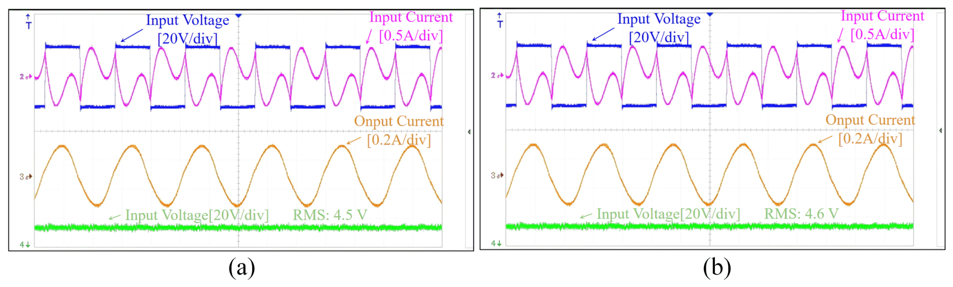
Figure 18 shows that the output voltage of the constant-voltage circuit stabilises at approximately 5 V and remains nearly unchanged as the load varies. The input voltage and the resonant-circuit input current are also largely in phase, indicating resonant operation. These results demonstrate that the dynamic compensation capacitor maintains a stable constant-voltage output over the tested load range by adjusting the equivalent impedance. Offset conditions were then evaluated using Rload = 20 Ω. The inverter and load waveforms under 5 cm lateral and longitudinal offsets are shown in Figure 19.
Figure 19 shows that the system still maintains resonant operation under the tested offsets: the input voltage and current remain nearly in phase, and the output voltage shows only slight fluctuation. The experimental results, therefore, indicate that the dynamic compensation method can compensate for mutual-inductance variation and maintain stable output under the tested offset conditions.

5.3. Efficiency Analysis and Discussion

The transmission efficiency was measured under different operating conditions. Figure 20 compares the efficiency results and summarises the overall system performance.
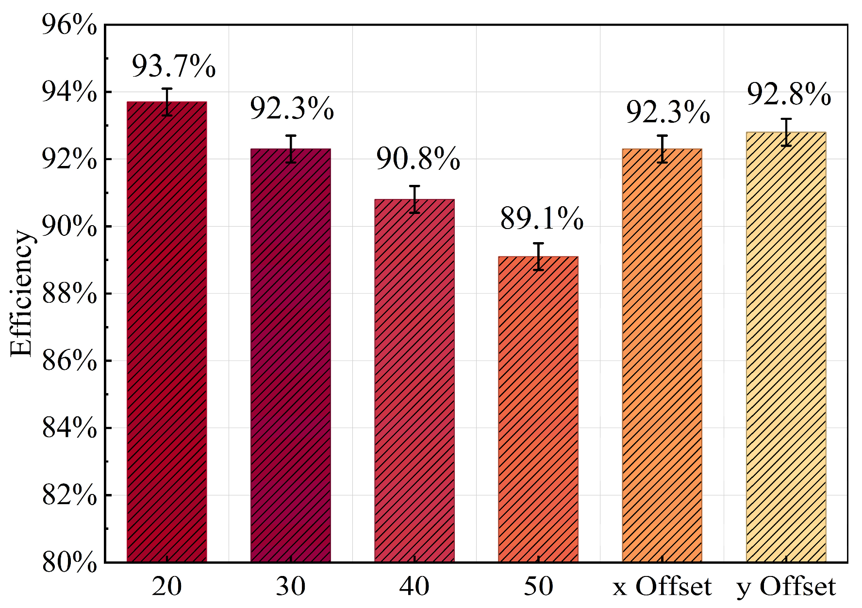
Figure 20 shows that as the load resistance increases from 20 Ω to 50 Ω, the efficiency decreases from 93.7% to 89.1%. The peak efficiency is reported as 93.7% ± 0.4 percentage points, and the error bars in Figure 20 represent the standard deviation of five repeated measurements. At high load resistance, the variation in reflected impedance causes the inverter operating point to deviate from the optimum ZVS region, increasing turn-on and turn-off overlap loss and making switching loss a major contributor to the efficiency reduction. This explanation is also consistent with Figure 18, where the voltage and current remain close to resonance under different loads, while the efficiency still decreases near the high-resistance boundary. To broaden the ZVS range over the full load range, future work will consider two strategies: adaptive inverter tuning based on load sampling to adjust dead time and switching timing, and coordinated DCCM with small-range phase-shift control to restore resonance matching and further compensate for phase deviation. Under offset conditions, the efficiency drops to 92.3% and 92.8%; nevertheless, dynamic compensation still maintains resonance matching, keeps efficiency above 89%, and preserves constant-voltage output.
The magnetic-flux-density simulation in Section 2.3 shows that the local flux density in the densely wound region reaches approximately 2.5–3.0 × 10³ μT, much higher than the 0.5–1.0 × 10³ μT in the central and loosely wound regions. According to the regional eddy-current loss model in Section 2.2, the single-turn eddy-current loss Peddy,single and the regional loss terms in Peddy,tot are related to the square of the local magnetic flux density Bm. Therefore, under similar conductor and geometric conditions, the local eddy-current loss tendency in the densely wound region can be estimated to be about 6.25–36 times that in the weak-flux region, indicating a higher thermal-stress tendency. Infrared temperature measurements under the rated operating condition showed that the maximum temperature rises in the densely and loosely wound regions were approximately 7 °C and 3 °C, respectively. The prototype therefore remained thermally stable under natural convection at room temperature. For future kilowatt-level operation, forced-air cooling and further winding optimisation will be considered to reduce local thermal stress and improve long-term reliability.
To further clarify the experimental difference between the proposed method and an LCC-S-based baseline, Table 4 compares this work with the experimental results reported in [29] from the perspectives of compensation strategy, control objective, coupling treatment, and experimental performance.
As shown in Table 4, the LCC-S baseline in [29] achieves wide output-voltage regulation and full-range ZVS through hybrid PSM and SCC control. In comparison, this work focuses on constant-voltage regulation under load and coupling disturbance. By introducing mutual-inductance variation into DCCM-based impedance compensation and ZVSA correction, the proposed method provides a coupling-aware dynamic compensation mechanism.
Table 5 compares the proposed method with representative WPT solutions. Conventional LCC-S compensation topologies often require more complex control or detuned operation. In contrast, the dynamic compensation capacitor proposed here adaptively adjusts the resonant condition around the nominal operating frequency. Within the tested load range and the specified lateral/longitudinal offsets, the system delivers stable, constant-voltage output, indicating a favourable balance between control simplicity and regulation performance.

6. Conclusions

This paper proposed a dynamically compensated constant-voltage WPT method based on non-uniform windings and parasitic coils. A region-based electromagnetic parameter model was established to characterise self-inductance, mutual inductance and coupling coefficients, and to explain the flux-compensation effect of the parasitic coils. An improved LCC-S topology with a dynamic capacitor compensation matrix was then introduced to compensate for resonance drift caused by load variation and coil-displacement-induced coupling changes, thereby maintaining resonant matching and constant-voltage output near the nominal operating frequency. In addition, a mutual-inductance-corrected zero-voltage-switching-angle tracking method was developed to compensate for phase deviation and maintain soft-switching operation. Simulations verified the constant-voltage characteristics, ZVSA tracking performance, and robustness of the proposed strategy under parameter variations. Prototype experiments showed stable constant-voltage output under load variation and 5 cm lateral and longitudinal offsets, with measured efficiency above 89% and a peak value of 93.7%.
Future work will extend the present region-based modelling framework from the single-transmitter–single-receiver structure to multi-receiver WPT systems. Based on the proposed partitioned modelling concept, multi-coil orthogonal arrangements and additional coupling correction factors will be introduced to quantify the parasitic cross-coupling among multiple receiver arrays. This extension will support multi-load experimental validation and provide a basis for full-domain decoupling design. In addition, the response speed and capacitance resolution of the dynamic capacitor compensation matrix will be further optimised.

Author Contributions

Conceptualization, L.G. and T.C.; Methodology, L.G. and T.C.; Software, L.G. and M.S.; Validation, L.G., C.G., M.S., and S.S.; Formal Analysis, L.G. and C.G.; Investigation, L.G., C.G., M.S., and S.S.; Resources, S.S. and T.C.; Data Curation, L.G., C.G., M.S., and S.S.; Writing—Original Draft Preparation, L.G.; Writing—Review and Editing, T.C.; Visualisation, L.G., C.G., M.S., and S.S.; Supervision, T.C.; Project Administration, T.C.; Funding Acquisition, T.C. All authors have read and agreed to the published version of the manuscript.

Funding

This work was supported in part by the National Natural Science Foundation of China under Grant 52307009, in part by the Hebei Province Yan Zhao Golden Terrace Talent Gathering Plan Key Talent Project under Grant B2024011, and in part by the Science Research Project of Hebei Education Department under Grant CXZX2026074.

Data Availability Statement

The data referred to in this paper may be obtained from the authors upon reasonable request.

Conflicts of Interest

The authors declare no conflicts of interest.

References

  1. Zhang, Z.; Pang, H.; Georgiadis, A.; Cecati, C. Wireless Power Transfer—An Overview. IEEE Trans. Ind. Electron. 2019, 66, 1044–1058. [Google Scholar] [CrossRef] [Scilit]
  2. Zhao, P.; Yu, L.; Liao, W.; Wang, J. Constant output voltage and non-communication-based maximum efficiency tracking for wireless power transfer systems: Single current control of primary-side. Energy Rep. 2023, 9, 200–212. [Google Scholar] [CrossRef] [Scilit]
  3. Lee, T.-S.; Huang, S.-J.; Wu, M.-J. Enhancement of Wireless Power Transfer for Automated Guided Vehicles Considering Disturbance Suppression. IEEE Access 2023, 11, 21508–21518. [Google Scholar] [CrossRef] [Scilit]
  4. Venkatesan, M.; R, N.; Kacor, P.; Vrzala, M. Bidirectional wireless power transfer: Bridging electric vehicles and the grid through converter analysis, coil topologies, and communication protocol review. Results Eng. 2025, 25, 103803. [Google Scholar] [CrossRef] [Scilit]
  5. Kraus, D.; Covic, G.A.; Herzog, H.-G.; Lawton, P.A.J.; Lin, F.J. Design and Assessment of an Interoperable Wireless Power Transfer System Using an Impedance-Based Method. IEEE Trans. Power Electron. 2023, 38, 2768–2781. [Google Scholar] [CrossRef] [Scilit]
  6. Yang, L.; Shi, Y.; Wang, M.; Ren, L. Constant Voltage Charging and Maximum Efficiency Tracking for WPT Systems Employing Dual-Side Control Scheme. IEEE J. Emerg. Sel. Top. Power Electron. 2022, 10, 945–955. [Google Scholar] [CrossRef] [Scilit]
  7. Huh, S.; Park, B.; Choi, S.; Shin, Y.; Kim, H.; Kim, J.; Park, J.; Park, D.; Ahn, S. Transmitter Coils Selection Method for Wireless Power Transfer System with Multiple Transmitter Coils and Single Receiver Coil. IEEE Trans. Power Electron. 2023, 38, 4092–4109. [Google Scholar] [CrossRef] [Scilit]
  8. Sagar, A.; Kashyap, A.; Nasab, M.A.; Padmanaban, S.; Bertoluzzo, M.; Kumar, A.; Blaabjerg, F. A Comprehensive Review of the Recent Development of Wireless Power Transfer Technologies for Electric Vehicle Charging Systems. IEEE Access 2023, 11, 83703–83751. [Google Scholar] [CrossRef] [Scilit]
  9. Zhang, X.; Xue, R.; Wang, F.; Xu, F.; Chen, T.; Chen, Z. Capacitor Tuning of LCC-LCC Compensated IPT System with Constant-Power Output and Large Misalignments Tolerance for Electric Vehicles. IEEE Trans. Power Electron. 2023, 38, 11928–11939. [Google Scholar] [CrossRef] [Scilit]
  10. Bodian, A.; Cardenas, A.; Ouardani, D.; Ouakrim, J.; Bennani-Ben Abdelghani, A. Implementing Wireless Charging System for Semi-Autonomous Agricultural Robots. Energies 2025, 18, 4624. [Google Scholar] [CrossRef] [Scilit]
  11. Xue, L.; Galigekere, V.P.; Gurpinar, E.; Su, G.-J.; Chowdhury, S.; Mohammad, M.; Onar, O.C. Modular Power Electronics Approach for High-Power Dynamic Wireless Charging System. IEEE Trans. Transp. Electrif. 2024, 10, 976–988. [Google Scholar] [CrossRef] [Scilit]
  12. Mansour, H.S.E.; Samir, M.; Elhady, B.; Abdelmaksoud, S. Wireless charging systems for electric vehicles: Review. Green Energy Intell. Transp. 2026, 5, 100371. [Google Scholar] [CrossRef] [Scilit]
  13. Chen, D.; Zhang, F.; Cui, J.; Bie, S.; Zhu, Z. A Novel Pendulum-Type Magnetic Coupler with High Misalignment Tolerance for AUV Underwater Wireless Power Transfer Systems. IEEE Trans. Power Electron. 2023, 38, 14861–14871. [Google Scholar] [CrossRef] [Scilit]
  14. Ali, A.; Saraereh, O.; Ware, A. Novel Design of Conical-Shaped Wireless Charger for Unmanned Aerial Vehicles. Energies 2025, 18, 5015. [Google Scholar] [CrossRef] [Scilit]
  15. Xu, H.; Huang, Z.; Li, X.L.; Tse, C.K. Misalignment-Tolerant IPT Coupler with Enhanced Magnetic Flux Variation Suppression and Reduced Copper Usage. IEEE Trans. Power Electron. 2024, 39, 10506–10517. [Google Scholar] [CrossRef] [Scilit]
  16. Yuan, Z.; Yang, Q.; Zhang, X.; Ma, X.; Wang, R.; Xue, M.; Zhang, P. A Misalignment-Tolerant Integrated S-S-S-Compensated WPT System with Constant Current Output. Energies 2023, 16, 2798. [Google Scholar] [CrossRef] [Scilit]
  17. Duan, X.; Han, W.; Hu, Y.; Tian, H.; Huang, J. 2-D Misalignment-Tolerant Wireless Power Transfer with a Compact O-to-OXY Magnetic Coupler. IEEE J. Emerg. Sel. Top. Ind. Electron. 2025, 6, 9–18. [Google Scholar] [CrossRef] [Scilit]
  18. Cai, L.; Mai, J.; Xu, D. A Quad-Quadrature Primary and Quadrature Secondary Magnetic Coupler for WPT System with High Misalignment Tolerance. IEEE Trans. Ind. Appl. 2026, 62, 1599–1606. [Google Scholar] [CrossRef] [Scilit]
  19. Zhang, Y.; Wei, G.; Zhang, J.; Hao, L.; Cheng, L. A Hybrid Topology Relay Based Wireless Power Transfer System with Mutual Inductance Enhancement and High Misalignment Tolerance. IEEE Trans. Power Electron. 2025, 40, 7640–7645. [Google Scholar] [CrossRef] [Scilit]
  20. Han, Y.; Tian, Z.; Li, L.; Li, S.; Yang, F.; Chen, J.; Fan, R.; Zhao, H. Decoupled dual-channel loosely coupled transformer with hybrid nanocrystalline and ferrite core for current sharing of modular wireless power transfer system. IET Power Electron. 2024, 17, 2238–2249. [Google Scholar] [CrossRef] [Scilit]
  21. Zhang, B.; Jiang, C.Q.; Yang, F.; Chen, C.; Lu, Y.; Zhou, J. An Antirotation Wireless Power Transfer System with a Flexible Magnetic Coupler for Autonomous Underwater Vehicles. IEEE Trans. Power Electron. 2025, 40, 2593–2603. [Google Scholar] [CrossRef] [Scilit]
  22. Zhao, P.; Liang, J.; Wang, H.; Fu, M. Detuned LCC/S-S Compensation for Stable-Output Inductive Power Transfer System Under UltraWide Coupling Variation. IEEE Trans. Power Electron. 2023, 38, 12342–12347. [Google Scholar] [CrossRef] [Scilit]
  23. Cai, C.; Wang, J.; Saeedifard, M.; Zhang, P.; Chen, R.; Zhang, J. Gyrator-Gain Variable WPT Topology for MC-Unconstrained CC Output Customisation Using Simplified Capacitance Tuning. IEEE Trans. Ind. Electron. 2024, 71, 3594–3605. [Google Scholar] [CrossRef] [Scilit]
  24. Zhang, Y.; Wei, G.; Zhi, X.; He, H. All-Detuned LCC-S-S Three-Coil Wireless Power Transfer System for Rack-and-Pinion Modules. Energies 2025, 18, 4397. [Google Scholar] [CrossRef] [Scilit]
  25. Stankiewicz, J.M. Evaluation of the Influence of the Load Resistance on Power and Efficiency in the Square and Circular Periodic WPT Systems. Energies 2023, 16, 2950. [Google Scholar] [CrossRef] [Scilit]
  26. Xu, J.; Li, X.; Li, H.; Xie, Z.; Ma, Q. Maximum Efficiency Tracking for Multitransmitter Multireceiver Wireless Power Transfer System on the Submerged Buoy. IEEE Trans. Ind. Electron. 2022, 69, 1909–1919. [Google Scholar] [CrossRef] [Scilit]
  27. Xu, F.; Zheng, H.; Zhang, X.; Chen, Z. Multiobjective Optimization with Minimum Output Error and Maximum Efficiency for WPT Systems Based on Discrete Neighborhood Search–Model Predictive Control Scheme. IEEE Trans. Ind. Electron. 2026, 73, 6939–6950. [Google Scholar] [CrossRef] [Scilit]
  28. Xia, C.; Chen, Y.; Sun, A.; Cao, Y.; Wang, X.; Wang, Q. Switching Frequency Control Strategy of Inverter for Multifrequency Multiload WPT System Based on Hysteresis Current Control. IEEE Trans. Power Electron. 2024, 39, 13946–13961. [Google Scholar] [CrossRef] [Scilit]
  29. Wang, X.; Xu, J.; Leng, M.; Ma, H.; He, S. A Hybrid Control Strategy of LCC-S Compensated WPT System for Wide Output Voltage and ZVS Range with Minimised Reactive Current. IEEE Trans. Ind. Electron. 2021, 68, 7908–7920. [Google Scholar] [CrossRef] [Scilit]
  30. Huh, S.; Ahn, D. Two-Transmitter Wireless Power Transfer with Optimal Activation and Current Selection of Transmitters. IEEE Trans. Power Electron. 2018, 33, 4957–4967. [Google Scholar] [CrossRef] [Scilit]
  31. Zhu, G.; Dong, J.; Shi, W.; Soeiro, T.B.; Xu, J.; Bauer, P. A Mode-Switching-Based Phase Shift Control for optimised Efficiency and Wide ZVS Operations in Wireless Power Transfer Systems. IEEE Trans. Power Electron. 2023, 38, 5561–5575. [Google Scholar] [CrossRef] [Scilit]
  32. Ma, T.; Jiang, C.; Xiang, J.; Wang, X.; Chau, K.T.; Long, T. modelling and Analysis of Wireless Power Transfer System Via Unified Full-Load Discrete-Time Model. IEEE Trans. Ind. Electron. 2023, 70, 5626–5636. [Google Scholar] [CrossRef] [Scilit]
Figure 1. Overall framework of the proposed WPT system.
Energies 19 02925 g001
Figure 2. Structure and parameter definitions of the proposed coupling mechanism.
Energies 19 02925 g002
Figure 3. Coupling coefficient as a function of coil structural parameters: (a) densely wound turns; (b) loosely wound turns; (c) parasitic-coil turns; (d) spacing in the densely wound region; (e) spacing in the loosely wound region.
Energies 19 02925 g003
Figure 4. Verification of the proposed electromagnetic model: (a) self-inductance; (b) mutual inductance; (c) coupling coefficient.
Energies 19 02925 g004
Figure 5. Finite-element verification of the magnetic flux density distribution in the partitioned coils. (a) Magnetic flux density distribution of the non-uniform winding structure without parasitic coil; (b) magnetic flux density distribution with parasitic coil compensation.
Energies 19 02925 g005
Figure 6. Overall flowchart of the composite control strategy.
Energies 19 02925 g006
Figure 7. Modified LCC-S compensation topology.
Energies 19 02925 g007
Figure 8. Structure of the dynamic capacitance compensation matrix.
Energies 19 02925 g008
Figure 9. Characteristics of compensation capacitance C1a,opt as a function of offset and load.
Energies 19 02925 g009
Figure 10. Comparison of ZVSA tracking performance under coupling-parameter disturbance.
Energies 19 02925 g010
Figure 11. Load-characteristic analysis: (a) output voltage versus resistance; (b) output current versus resistance; (c) output power versus resistance; (d) system efficiency versus resistance.
Energies 19 02925 g011
Figure 12. Dynamic response of the output voltage under load-step conditions.
Energies 19 02925 g012
Figure 13. Parameter sensitivity based on output-voltage stability.
Energies 19 02925 g013
Figure 14. Parametric response of system output and efficiency: (a) robustness analysis; (b) frequency-response analysis.
Energies 19 02925 g014
Figure 15. Comprehensive distribution of system efficiency. (a) Three-dimensional efficiency distribution with respect to load resistance and mutual inductance; (b) corresponding efficiency contour plot.
Energies 19 02925 g015
Figure 16. Predicted performance maps under extended lateral and longitudinal misalignment within 0–10 cm: (a) fitted coupling coefficient; (b) simulated output voltage; (c) estimated efficiency.
Energies 19 02925 g016
Figure 17. Experimental platform for the WPT system.
Energies 19 02925 g017
Figure 18. Experimental waveforms under different loads (a) Rload = 20 Ω, (b) Rload = 30 Ω, (c) Rload = 40 Ω, (d) Rload = 50 Ω.
Energies 19 02925 g018
Figure 19. Experimental waveforms of the inverter and load under displacement (a) Δx = 5 cm (b) Δy = 5 cm.
Energies 19 02925 g019
Figure 20. Variation in output efficiency under different operating conditions.
Energies 19 02925 g020
Table 1. Design parameters of the coupling mechanism.
ComponentValueComponentValue
N15d11 mm
N24d23 mm
Np3l1300 mm
l2400 mmlp1150 mm
lp2250 mm//
Table 2. Simulation circuit parameters.
ComponentValueComponentValue
UDC50 VLf130 μH
L1193.07 μHLf220 μH
L2242.92 μHC1116.8 nF
M43.045 μHC230.2 nF
C1aDynamic//
Table 3. Experimental parameters.
ComponentValueComponentValue
UDC20 VLf130 μH
L194.8 μHLf220 μH
L2116 μHC1117 nF
M21 μHC230 nF
C1aDynamic//
Table 4. Experimental comparison between the LCC-S baseline and this work.
ItemLCC-S Baseline in [29]This Work
Compensation topologyLCC-SImproved LCC-S
Control strategyPSM + SCC hybrid controlDCCM + mutual-inductance-corrected ZVSA
Main control objectiveWide output-voltage regulation and
full-range ZVS
Constant-voltage regulation under load and coupling variation
Coupling treatmentCoupling coefficient is considered as a system parameterMutual-inductance variation is introduced into compensation and ZVSA correction
EfficiencyPeak efficiency 94.7%Above 89%, peak 93.7%
Dynamic responseVoltage-step response about 35 ms; load-step response about 42 msZVSA recovery about 10 ms under coupling disturbance
Soft-switching resultFull-range ZVS; Izvs maintained around 2 AZVSA phase returns to the reference value under coupling disturbance
Table 5. Comparison of existing WPT methods and the proposed approach.
Ref.TopologyCouplerControl StrategyFrequency ControlEfficiencyRemarks
[17]S-SOXY couplerStructural optimisationFixed88%Structure-oriented design without active regulation
[19]Hybrid topologyThree-coil structure with receiver-side relay coilMutual inductance regulation via dual adjustment factorsResonant condition with parameter tuning93.05–93.29%MI-enhancement and misalignment-tolerant design with dual-parameter flexibility
[22]LCC/S-SConventional coilDetuned designDetuned93%Detuning-based operation
This WorkImproved LCC-SProposed hybrid coilDynamic capacitor compensation matrix Capacitance tuning near nominal frequencyUp to 93.7%DCCM- and ZVSA-based constant-voltage regulation
Disclaimer/Publisher’s Note: The statements, opinions and data contained in all publications are solely those of the individual author(s) and contributor(s) and not of MDPI and/or the editor(s). MDPI and/or the editor(s) disclaim responsibility for any injury to people or property resulting from any ideas, methods, instructions or products referred to in the content.