Article

Wide Voltage Gain Range Bidirectional DC-DC Converter with Reduced Switches Count and Buck-Boost Characteristic in Both Power Flow Directions

by
Victor Fernão Pires
1,2,
Armando Cordeiro
2,3,
Daniel Foito
1,4,*,
Tito Amaral
1 and
José Fernando Silva
2,5
1
ESTSetubal, Polytechnic Institute of Setúbal, 2914-508 Setúbal, Portugal
2
INESC-ID, 1000-029 Lisboa, Portugal
3
ISEL, Lisboa Polytechnic University, 1549-020 Lisboa, Portugal
4
CTS-UNINOVA and LASI, 2829-516 Caparica, Portugal
5
IST, Lisboa University, 1049-001 Lisboa, Portugal
*
Author to whom correspondence should be addressed.
Energies 2026, 19(1), 43; https://doi.org/10.3390/en19010043 (registering DOI)
Submission received: 14 September 2025 / Revised: 2 December 2025 / Accepted: 18 December 2025 / Published: 21 December 2025
(This article belongs to the Special Issue Design and Control Strategies for Wide Input Range DC-DC Converters)

Abstract

Several applications require bidirectional power converters with high-voltage gain. While several topologies have been proposed, none of them exhibit Buck-Boost characteristics in both forward and reverse power transfer. Most proposals behave as a Boost converter in forward direction and as a Buck converter in the reverse direction. Therefore, this paper proposes a novel DC-DC bidirectional power converter that exhibits Buck-Boost characteristics in both power flow directions while providing very high wide voltage gain range. The proposed converter has, in addition, the ability to maintain continuous currents in the input and output. The theoretical analysis of the converter under bidirectional power flow conditions will be presented and examined, along with the design of its components. The validation of the characteristics and behavior of the proposed bidirectional power converter were tested in several laboratory experiments. The experimental results obtained from both power flow directions show agreement with the theoretical considerations.

1. Introduction

The importance of power electronic converters is globally increasing year after year because of the widespread usage of renewable energy sources (RES), energy storage systems (ESS), Electric Vehicles (EVs), consumer electronics, aerospace and defense, and massive electrification of manufacturing structures [1,2,3]. Due to particular electric requirements across different applications, a significant amount of generated or consumed power needs are expected to be processed using some type of power electronic converter [4,5]. Many power electronic converter topologies are only able to provide unidirectional power flow according to the application requirements. Nevertheless, in a worldwide search for clean and renewable power sources and energy efficiency, because of the climate and energy crisis, the demand for advancing the development of converter topologies with bidirectional power flow capabilities has become increasingly imperative. This is particularly important in the transportation sector, where bidirectional power flows enable the application of traction and energy recovery during various routes, thereby optimizing energy resources [6,7]. This aspect is also crucial in the energy sector, where the effective implementation of local or decentralized smart-grids or microgrids is only possible due to power electronic converters with the ability to provide the bidirectional power transfer feature [8,9]. Furthermore, it is common to employ power electronic converters for auxiliary purposes, such as ensuring voltage stability and equalization, load regulation, compensating for reactive power and harmonics, or implementing filtering capabilities, among other possibilities [10,11].
Several bidirectional isolated and non-isolated types of power electronic converter topologies have been proposed for several AC and DC applications over the last years [12,13]. Regarding isolated bidirectional DC-DC converters, some of the most popular topologies are the bidirectional Dual Active Bridge (DAB), Flyback, Cuk or Sepic/Zeta, Push-Pull, Forward, and resonant converters [14,15]. Most of those topologies are also obtained from traditional isolated DC-DC converters. Despite their higher cost, isolated topologies typically offer two power conversion stages with galvanic separation through a high-frequency transformer [16,17,18]. This will lead to converters that have a higher component count and cost, exhibiting increased size and weight. In fact, high power density cannot be expected from isolated DC-DC converters due to their capacitive, magnetic, and thermal management components [19]. The number of power devices can be relatively significant in some isolated DAB topologies. However, DAB is an established topology known for its high-voltage gain capability [20,21,22]. Thus, in solutions that require galvanic isolation, this converter is one of the most important options [23]. It is important to mention that the DAB topology is not inherently limited to isolated versions [24,25,26]. In a non-isolated configuration, for example, the two active bridges and the transformer can be replaced with two active bridges connected directly through a single inductor. This structure still preserves the fundamental operating principle of the DAB: transferring power by controlling the phase shift between the square-wave voltages generated by the two active bridges across the inductor.
Regarding non-isolated bidirectional DC-DC converters, most known topologies were derived from traditional unidirectional DC-DC converters. This type of converter, on the other hand, features simpler designs, a smaller size, higher power density, and control systems compared to isolated topologies, making them suitable for applications where isolation is not required [20]. Indeed, they can be used in battery-powered devices, intermediate bus architectures, automotive electronics, telecom/datacom applications, and for boosting or lowering voltage within a common ground system. References [27,28,29,30] contain information on several well-known bidirectional non-isolated DC-DC converters. These include the Buck-Boost, Cuk, Sepic/Zeta, switched-capacitor, interleaved and coupled-inductor topologies, and others. Typically, devoid of high-frequency isolation transformers, these DC-DC converters are characterized by their simplicity and low cost. A comprehensive assessment of bidirectional non-isolated DC-DC converters featuring operation in ZVS (Zero Voltage Switching) or in ZCS (Zero Current Switching) can be found in [29]. Other modified topologies have been developed and presented over the last years based on those topologies, such as cell modified/hybrid switched-capacitor converters [31,32,33], soft-switching current fed LCL resonant converters [34], soft-switching coupled-inductor converters [35], and other modified topologies derived from the conventional Buck-Boost converter [36,37]. Those topologies are commonly used in low or medium power applications where safety concerns are not critical. Another focal aspect is the development of topologies with wide voltage gain, as shown, for example, in [38,39,40,41,42,43,44]. Most of these topologies are modified versions of the traditional bidirectional DC-DC converters, incorporating supplementary active and passive components. On the other hand, it should be noted that most of these converters offer step-down gain in forward power transfer and step-up gain in the reverse direction.
Multilevel bidirectional non-isolated DC-DC topologies can also be found in the literature, such as the flying capacitor based multilevel DC-DC converters (FCMDC) [45], the multilevel modular capacitor clamped DC-DC converter (MMCCC) [46], or bidirectional three-level cascaded (BTLC) converter [47]. Compared to the abovementioned non-multilevel converters, the magnetic-less flying or modular capacitor-based multilevel DC-DC present several advantages, including a reduced component count (switching devices and capacitors), lower voltage stress on power devices, and higher voltage gains. Still, these multilevel converters do have limited and unsymmetrical step-up and step-down conversion ratios. Certain multilevel solutions can achieve a continuous voltage gain range by adjusting the duty cycle. However, the control is complex, and the continuous range is limited due to significant dependency on parasitic resistance in the capacitor’s charging and discharging paths, as well as on the switching frequency. Furthermore, these multilevel converters exhibit pulsed input/output currents, which significantly diminish the lifespan of energy storage systems or energy sources [45]. Despite the multiple available solutions, there is still a need in most applications to develop new bidirectional DC-DC converters offering high-voltage gain and bidirectional variable range at a reduced component count. This requirement justifies ongoing research and development efforts in this field. A drawback of these converters is that a significant number of switches and passive components are typically needed when relatively high-voltage gains are required. Consequently, there is also a requirement to develop converters that can achieve high-voltage gain with reduced component counts.
In this paper, a novel bidirectional DC-DC converter is introduced, featuring high-voltage gain while reducing the switch and passive component count. The proposed topology is well-suited for applications needing bidirectional power flow and adjustable voltage range in both directions. One of the key characteristics of the proposed topology is its ability to operate in a bidirectional Buck-Boost mode, simultaneously offering continuous input and output current. This feature proves to be advantageous for numerous applications, including RES and ESS. To validate the hereafter theoretical assumptions, this paper presents several experimental results obtained from a laboratory prototype. These results show the performance effectiveness of the proposed converter.

2. Operation and Analysis of the Proposed Bidirectional DC-DC Converter

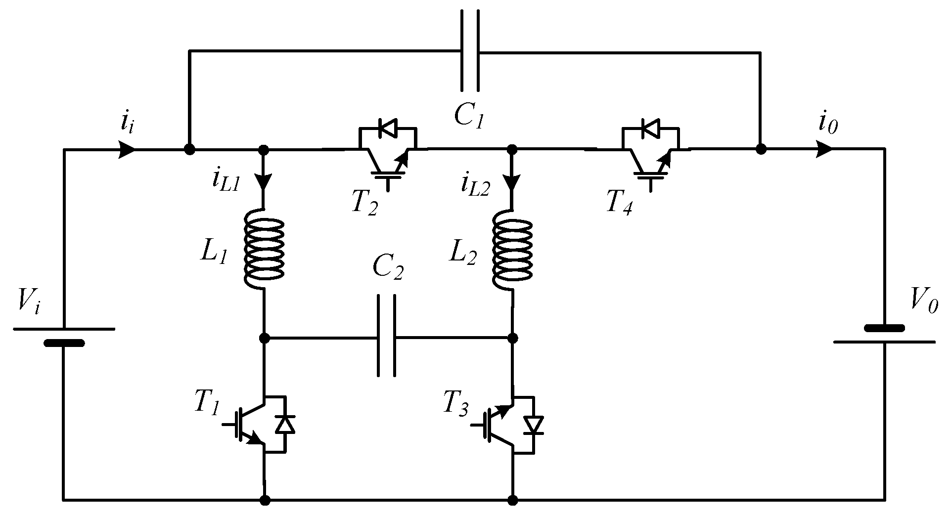
With Boost characteristics in reverse power flow and Buck characteristics in forward power flow, existing bidirectional DC-DC converters need cascaded structures to achieve high-voltage gain, which raises the number of switches and passive components and reduces efficiency. Consequently, a new bidirectional DC-DC converter is proposed in this paper with the goal of enabling Buck-Boost characteristics in both power flow directions while maintaining the simplicity and low component count of a single structure. The proposed structure only needs four transistors with antiparallel diodes, two inductors, and two capacitors, as shown in Figure 1. Due to the type and quantity of passive components, this converter is based on a 2L2C structure. It should be noted that the continuous currents in the input and output terminals (Vi and Vo) are also a key feature of the proposed converter.
The power semiconductors will be assumed to be ideal, and the series resistances of the inductors, capacitors and voltage sources will be assumed to be zero, helping to analyze and calculate the appropriate relationships between the converter input and output. The source/output capacitor voltages Vi and Vo are also considered constants.

2.1. Forward Energy Transfer Operation

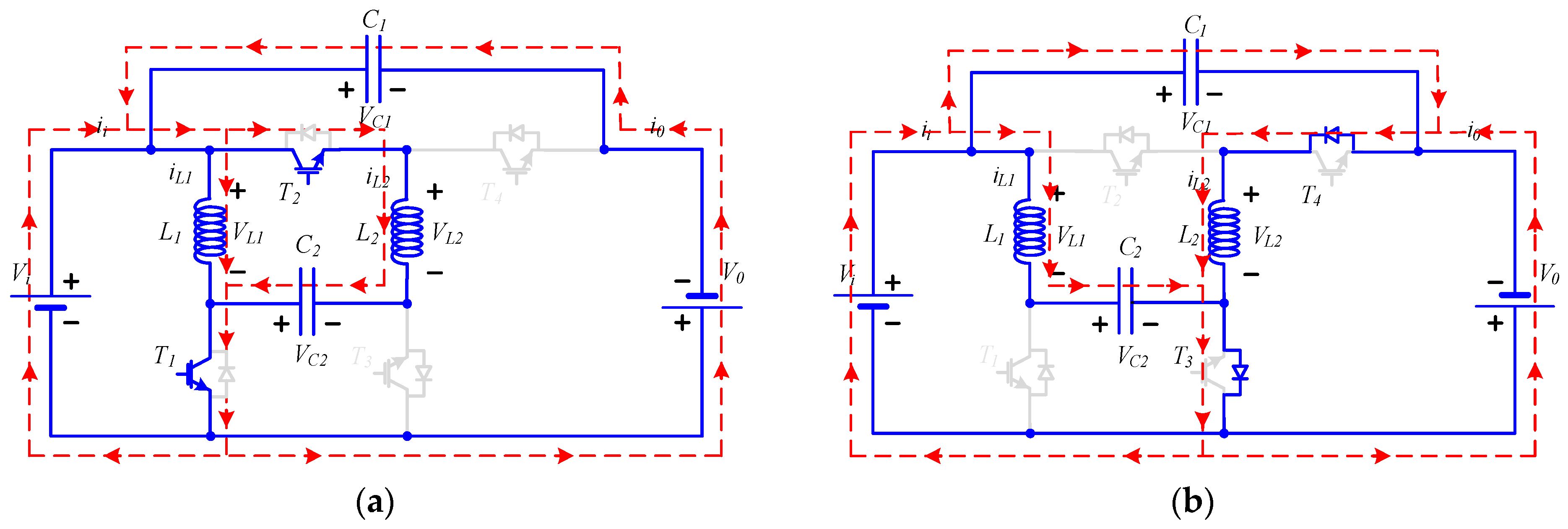
When power is transferred from the Vi input to the Vo output (forward transfer mode), the operation of the proposed DC-DC converter with bidirectional Buck-Boost mode is characterized by two modes. During Mode 1, transistors T1 and T2 are turned ON, and all other power semiconductors are turned OFF (Figure 2a). During Mode 2, diodes D3 and D4 are in ON state and all other power semiconductors are turned OFF (Figure 2b). Considering that the converter should operate in the continuous conduction mode (CCM), in steady state the converter operation and timing in Modes 1 and 2 can be described as:
Mode 1—The control signal for transistors T1 and T2 is δi-o (t) = 1, meaning that T1 and T2 are in the ON state while the remaining semiconductors are all in the OFF state. Therefore, both inductors will be charged by the input voltage source Vi and capacitor C2. Capacitor C1 will release energy into the load.
Mode 2—The control signal for transistors T1 and T2 is δi-o (t) = 0, meaning all power transistors are turned OFF, while only diodes D3 and D4 are conducting (ON state). As a result, the energy stored in the inductors will be released to the capacitor C2, the load, and C1.
To obtain the static voltage gain of the converter, the volt-second balance principle will be applied to the inductors [48]. Thus, the average voltage across the inductor (L) over one switching cycle must be zero, which means that:
1 T S 0 T S v L ( t ) d t = 0
In this way, by applying this principle to the inductors L1 and L2 and considering Modes 1 and 2 (see the voltages applied to the inductors in Figure 2), we have a positive voltage during the δi-o TS and a negative voltage during (1 − δi-o)TS. This can be expressed as follows:
V L 1 = δ i o V i + 1 δ i o V i V C 2
V L 2 = δ i o V i + V C 2 1 δ i o V o = 0
where δi-o represents the converter duty cycle in the forward energy transfer (δi-o = 〈δi-o (t)〉). From (2), the intermediate capacitor voltage C2 can be determined as:
V C 2   =   1 1 δ i o V i
Combining Expressions (3) and (4), the static voltage gain of this bidirectional Buck-Boost DC-DC converter, operating in the forward energy transfer mode, is given as:
G i n p u t o u t p u t =   V o V i   =   δ i o 2 δ i o 1 δ i o 2
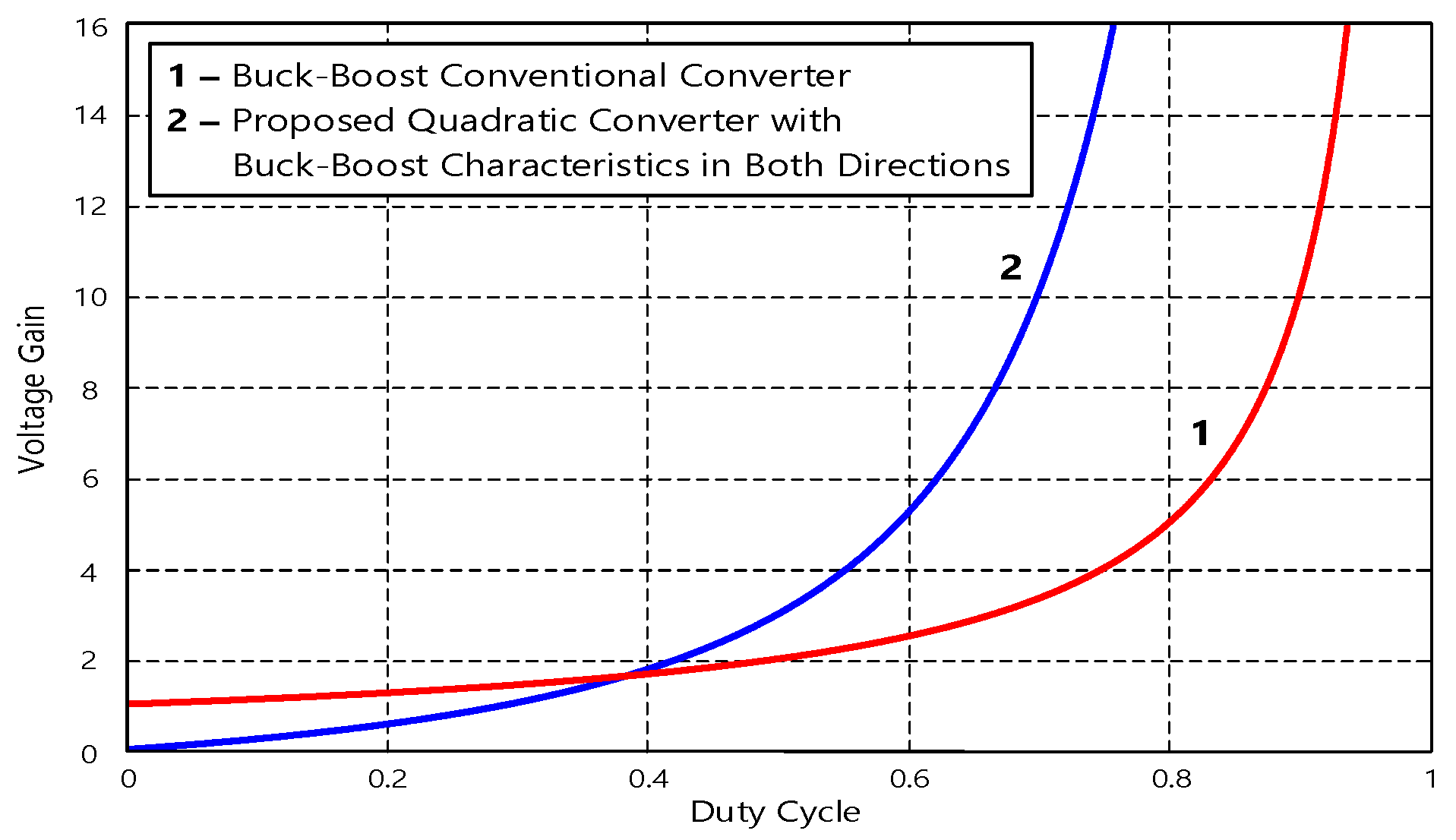
It is clear from the analysis of the output/input static voltage gain in Expression (5) that the proposed bidirectional Buck-Boost DC-DC converter, in the forward energy transfer mode, can be operated in either the Buck or in the Boost regions. Additionally, Expression (5) shows that the proposed bidirectional Buck-Boost DC-DC converter can present high-voltage gains, due to the quadratic δi-o term. This is illustrated in Figure 3, which compares the voltage gains of the present converter and the conventional bidirectional Buck-Boost converter. The figure clearly shows that the conventional bidirectional Buck-Boost converter is limited to Boost operation when energy is transferred from input to output. Conversely, the proposed converter supports Buck-Boost mode operation.

2.2. Reverse Energy Transfer Operation

In this operation mode, power is transferred from the Vo output to the Vi input (reverse transfer mode). In this scenario, transistors T3 and T4 will be turned ON during Mode 1, with all other power semiconductors turned OFF (Figure 4a). During Mode 2, diodes D1 and D2 are ON and all other power semiconductors are OFF (Figure 4b). The converter operation in reverse energy transfer and timing in Modes 1 and 2 can be described as:
Mode 1—The control signal for transistors T3 and T4 is δo-t (t) = 1, meaning that T3 and T4 are turned ON, while the remaining semiconductors are turned OFF. Therefore, both inductors will be charged by the bus (Vo) and capacitor C2. On the other hand, capacitor C1 will discharge to the input side and inductor L2.
Mode 2—In this second operation mode, the power diodes D1 and D2 are turned ON, while all other power semiconductors will be turned OFF. In this way, the energy that was stored in the inductors will be released to the input power source, capacitors C1 and C2.
Supposing CCM and steady state, the volt-second balance on the inductors L1 and L2, considering the reverse energy transfer Modes 1 and 2, gives:
V L 1   =   δ o i V C 2 V i 1 δ o i V i   =   0
V L 2 = δ o i V o 1 δ o i V i + V C 2
where δo-t (δo-t = 〈δo-t (t)〉) is the converter duty cycle in the reverse energy transfer. From (6), the intermediate capacitor C2 voltage is written as:
V C 2   =   1 δ o i V i
Thereby, from the expressions in (6), the static voltage gain of this bidirectional Buck-Boost DC-DC converter, operating in the reverse energy transfer mode, is given as:
G o u t p u t i n p u t =   V i V o   =   δ o i 2 1 δ o i 1 + δ o i
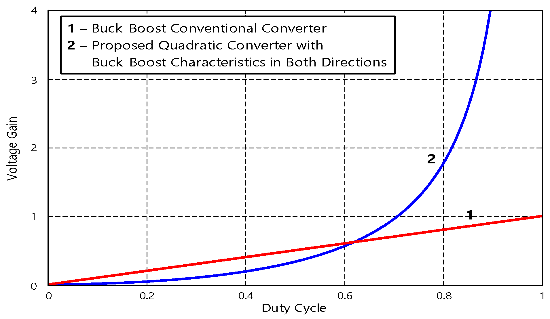
Expression (9) shows that the static voltage gain of the input and output in the reverse energy transfer mode exhibits Buck-Boost characteristics with high gain as well (Figure 5). For comparison, the input-output static voltage gain of the conventional Buck-Boost converter is also shown in Figure 5. As in the previous case, this figure shows the limitations of the conventional bidirectional Buck-Boost converter, as it only operates in Buck mode when energy is transferred from output to input. In contrast, the proposed converter allows for Buck-Boost mode operation.

3. Design of the Bidirectional Converter with Buck-Boost Characteristics in Both Directions

3.1. Passive Components

It is possible to design the passive components (capacitors and inductors) considering their maximum voltage and current ripples, ΔVC and ΔiL, respectively. In the case of capacitors, their capacitance is obtained considering that their voltage ripples, ΔVC1 and ΔVC2, are a small percentage of the respective capacitor average voltages (VC1, VC2). Thus, assuming capacitor voltages with small linear variation, the voltage ripples can be estimated using the following expressions, which are related to the switching ON time, ΔtON, (ΔtON = δT = δ/fPWM):
Δ V C 1 =   δ i o   I o C 1   f P W M   =   1 δ i o I o C 1   f P W M
Δ V C 2 = δ i o   I L 2 C 2   f P W M = 1 δ o i I L 2 C 2   f P W M
While capacitor C1 can be obtained from Expression (9), capacitor C2 in (11) is dependent on the inductor L2 current. To obtain the inductor current IL2, the ampere-second balance in capacitors C1 and C2 is used. Therefore, the obtained current is given in Expression (12) and the C2 capacitance value can be obtained from a predefined capacitor ripple, as presented in Expression (13).
I L 2 = I o 1 δ i o = I o δ o i
Δ V C 2 = I o C 2   f P W M   δ i o 1 δ i o = I o C 2   f P W M   δ o i 1 δ o i
Similar steps can be taken to calculate the inductor values, considering their maximum current ripples (ΔIL1 and ΔIL2) as a percentage of the inductor average currents. Inductor currents are also thought to exhibit small linear variations. In this way, the following expressions can be used to estimate the inductors value based on the current ripples related to the switching ON time ΔtON, (ΔtON, = δT = δ/fPWM):
Δ I L 1 =   δ i o   V i L 1   f P W M   =   1 δ o i V i L 1   f P W M
Δ I L 2 = 1 δ i o   V o L 2   f P W M = δ o i   V o L 2   f P W M

3.2. Power Semiconductors

The maximum voltage and current stresses to which the power semiconductors will be subjected are calculated using the Kirchhoff voltage and current laws, as well as the turning ON and turning OFF times of the switches. The transistor voltage and current stresses are given as Expressions (16) and (17):
V T 1 =   V T 3   =   V C 2   =   1 δ i o δ i o V o V i =   1 2 δ o i δ o i V i V T 2 =   V T 4   =   V i + V o
I T 1 = δ i o 1 δ i o 2 I o = 1 δ o i δ o i 2 I o I T 2 = δ i o 1 δ i o I o = 1 δ o i δ o i I o I T 3 = 1 1 δ i o I o = 1 δ o i I o I T 4 = 1 δ i o δ i o 2 I o
According to our assessment and analysis of the circuit, voltage and current stress over power devices do not seem to reveal excessive stress values when compared to other solutions. This can be seen through the comparison with, for example, topology proposed in [32]. Thus, considering the same output power (500 W), same input voltage (24 VDC), and same output voltage (400 V), reference [32] presents theoretical values of 534 VDC and 26,5 A for the maximum voltage and maximum current stress over a certain power device in the worst scenario, while the proposed topology presents 224 VDC and 1,83 A. Nevertheless, multiple aspects can be improved to reduce or mitigate the voltage and/or current stress over the main components, namely through the improvement of their thermal management, reducing the layout of the circuits to reduce eventual loop inductance, adding proper snubbers/clamps devices (e.g., RCD/snubber, RC snubber, or active clamp depending on topology), and choosing power devices suited to low stress using SiC or GaN for lower switching energy and less reverse recovery. Applying ZVS/ZCS when necessary (e.g., LLC, resonant converters) to reduce switching losses and voltage stress or using EMI (Electromagnetic Interference) filters and common-mode chokes to reduce emissions and unintended high dv/dt coupling to other circuits are possible solutions.

4. Comparison to Similar Topologies

In this section, a comparative study is carried out to evaluate the benefits and drawbacks of the proposed non-isolated bidirectional DC-DC converter. Several aspects are considered as a basis for comparison, including voltage gain in forward and reverse energy transfer operation, control complexity, maximum voltage and current stress, the number of power switches, capacitors, inductors, and coupled inductors. Table 1 contains the summary of this comparative study. One feature that can be seen in Table 1 is that the proposed topology allows for a wide voltage gain range in both directions. It is also distinguished by its low control complexity, as only the duty cycle needs to be adjusted. Additionally, it is one of the topologies that require the least number of passive components, when compared to other solutions. In this comparison, the control complexity is related with the modulation adopted and requirement of multiple switching stages to achieve ZVS or the multiple combination of power devices. Also, the control complexity of the converters is considered high when specific designed blocks are required, or they need independent control loops (for power sharing, voltage, current, etc.), increasing the number of interacting control variables, or even when they require advanced control strategies (e.g., decoupling, multi-variable control, or model predictive control).
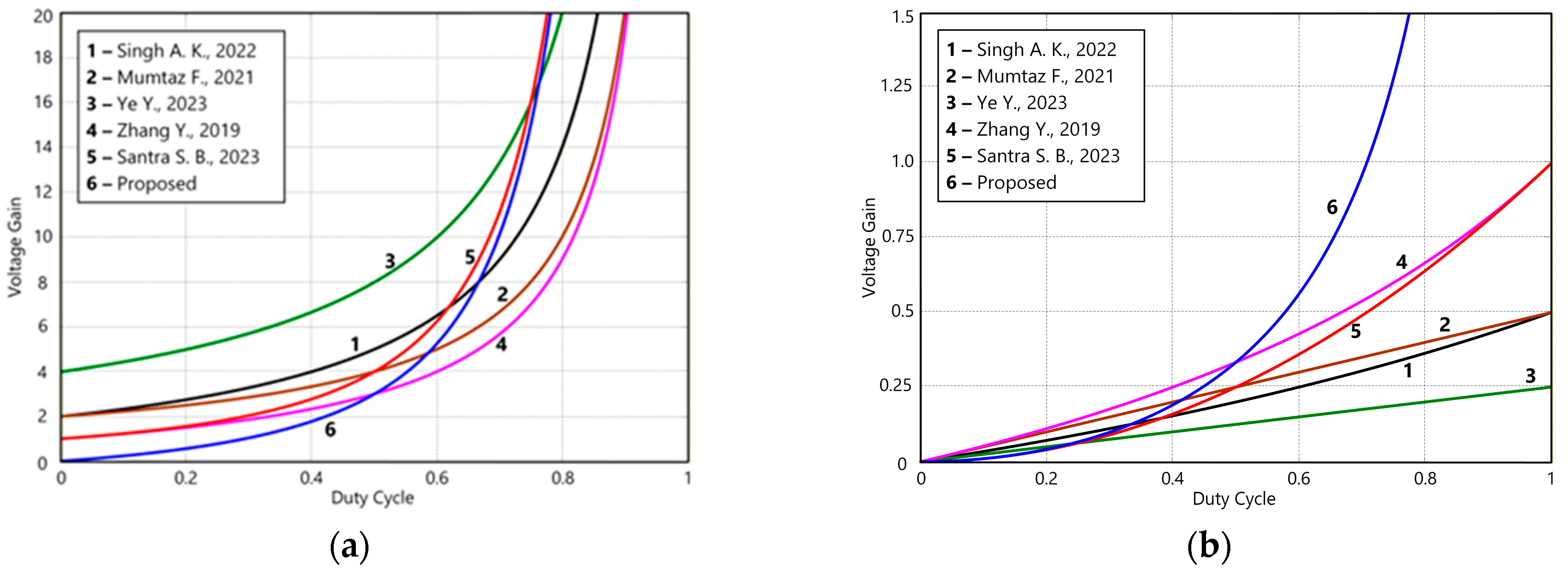
To analyze the static voltage gain versus duty cycle between the proposed and the other bidirectional Buck-Boost converters described in Table 1, Figure 6 presents a chart illustrating this relation for both forward and reverse energy transfer operations. Thus, analyzing Figure 6a for the forward energy transfer mode, it is evident that the proposed topology ranks as the one with the highest static voltage gain. However, when compared to the topology with the highest static voltage gain, it is possible to see that the proposed design exhibits Buck-Boost characteristics, while the other does not. Additionally, beyond this characteristic, the proposed design also presents a wider range. On the other hand, analyzing the reverse energy transfer mode shown in Figure 6b, it is evident that it is one of the top configurations allowing for greater reduction due to the quadratic gain. The topology that presented higher static voltage gain in the forward energy transfer operation, does not present a reduction as high as the one proposed in Buck mode. On the other hand, the proposed topology still presents Buck-Boost characteristics, even in this reverse energy transfer mode.

5. Simulation Tests

Several simulation tests under different operating conditions were performed on a computer simulation platform to validate the theoretical assumptions. The proposed bidirectional Buck-Boost DC-DC converter was implemented in PLECS® simulation software Version 4.9.8. Table 2 shows the parameters of the converter components as well as the operation specifications adopted in the simulation. It is important to mention that, as previously verified, the adopted switching frequency is a function of the design of the components. In this case, optimization was not performed, as the objective is to validate the proof of concept.
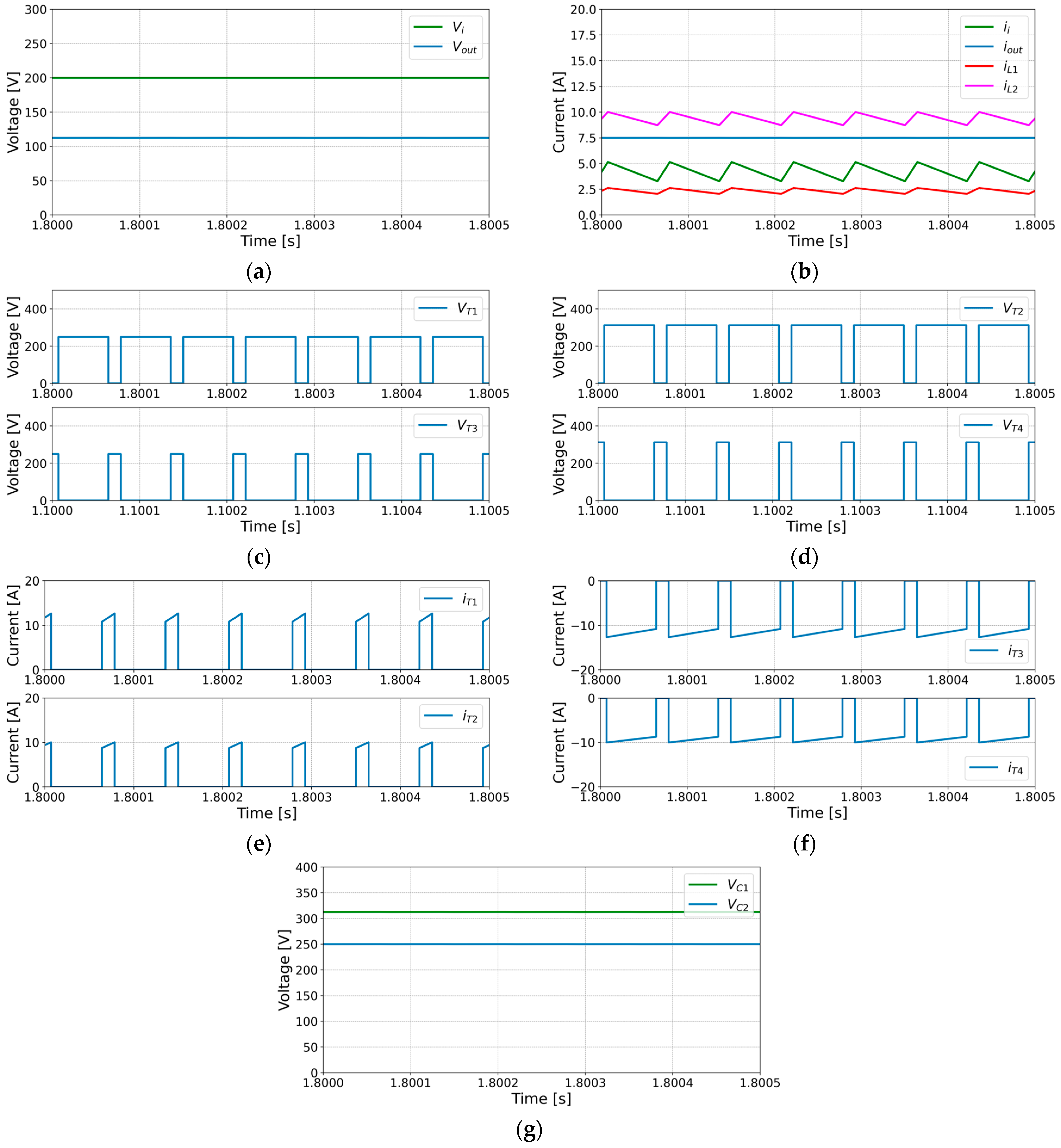
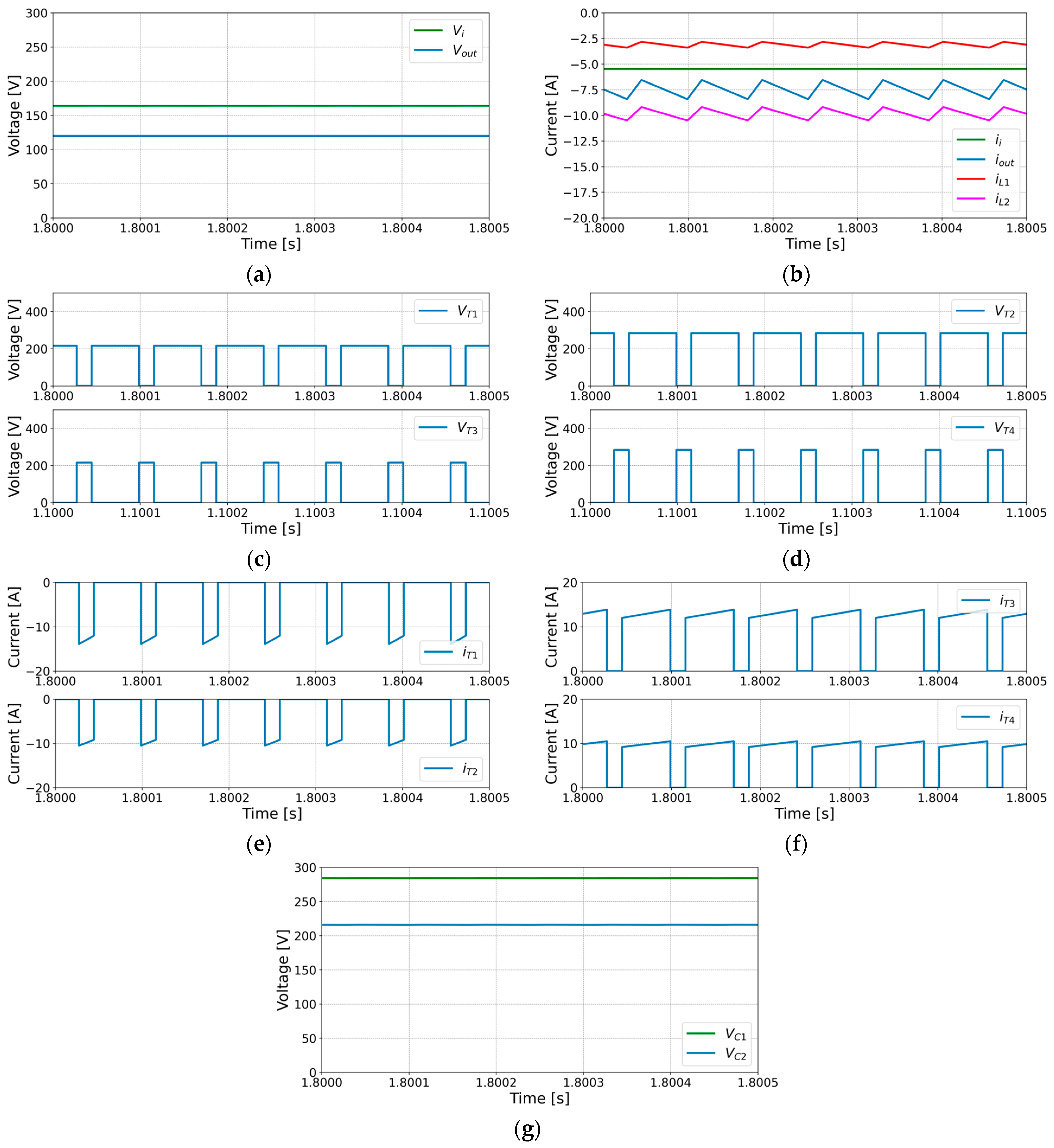
In the first set of simulations, the proposed bidirectional Buck-Boost DC-DC converter topology was simulated in forward energy transfer mode. The waveforms obtained from this test in steady state and for the operation specifications of Table 2 can be seen in Figure 7. For this test, a duty cycle of 0.67 was used for transistors T1 and T2. Figure 7a illustrates that the input and output voltages show agreement with the converter parameters and duty cycle of the transistors T1 and T2, in accordance with the voltage gain given by Equation (5). Moreover, the input current presents no discontinuities (continuous current, Figure 7b. This is an important feature in applications where the input contains an energy storage battery, for example. Another advantage is that the output current is also continuous. The current inductors can also be seen in Figure 7b, illustrating their continuous waveforms. The transistors T1 and T2 voltage waveforms are also shown in Figure 7c,d, confirming that the transistor T2 must withstand the output voltage, while transistor T1 must withstand a much lower voltage. It is also possible to observe that T1 and T2 operate synchronously, as the transistor voltage waveforms illustrate. The currents through the transistors are also shown in Figure 7e. Since only transistors T1 and T2 operate in this mode, the currents in the other transistors flow through their internal diodes. As a result, they show negative values, as illustrated in Figure 7f These waveforms confirm that the transistor with the highest current is T1. The voltages across the capacitors are also displayed in Figure 7g. These waveforms show that capacitor C1 experiences the most voltage stress, while capacitor C2 experiences significantly reduced voltage stress.
As mentioned in the study of the proposed DC-DC converter, one of its characteristics is its capability to operate in Buck-Boost mode in both directions. Thus, another simulation test was performed to verify this operability. Figure 8 shows the results obtained under conditions where the duty cycle is 0.2 and the input voltage is 120 V. From this figure, it is possible to see that, contrary to the previous test, the circuit now operates in Buck condition. The behavior of the voltages across the transistors and the currents through them is similar, as verified by the previous test. The same applies to the voltage stress across the capacitors, confirming that it is again higher for capacitor C1.
Simulations with the bidirectional Buck-Boost DC-DC converter operating in reverse energy transfer mode were also performed, using the same converter parameters listed in Table 2. Figure 9 shows the waveforms obtained for these tests in steady state and with a duty cycle of 0.33. When seen from the converter output (Vo) side to the input (Vi) side, a high-voltage gain reduction is noticed (see Figure 9a). The current injected into the input voltage source remains continuous, indicating that this converter is suitable for battery applications or other applications requiring continuous currents. The current at the output terminals is also continuous, as are the currents in the inductors. The inversion of the currents presented in Figure 9b indicates the reverse energy transfer mode. The blocking voltages in transistors T3 and T4 are also visible, showing that transistor T3 needs to withstand a lower voltage while transistor T4 needs to withstand a higher voltage, namely the capacitor C1 voltage. The current waveforms in all the transistors and voltage over capacitors are available in Figure 9e–g.
Additional simulation tests were performed to confirm the Buck-Boost characteristic of this converter in reverse energy transfer mode. Figure 10 shows the results obtained for the condition in which the duty cycle is 0.67. From this figure, it is possible to see that, in contrast to the previous test, the circuit now operates in Boost mode. Despite different average current and voltage values and different duty cycle, the waveforms have similar behavior when compared to Figure 9.
Additionally, the proposed bidirectional Buck-Boost DC-DC converter was also simulated in different transient conditions. In this context, the first test was performed with the converter operating in the forward energy transfer mode, where several step changes in the duty cycle were considered, specifically from 0 to 0.4, 0.5, 0.6 and ending at 0.45. The resulting waveforms of this test can be seen in Figure 11, confirming the changes in the output voltages in response to duty cycle variations (see Figure 11a) and the input and output continuous currents (see Figure 11b), which also change their values in response to the respective duty cycle variations, while always remaining without discontinuities. The bidirectional Buck-Boost DC-DC converter was also simulated in transient conditions in the reverse energy transfer mode. Again, similar step changes in the duty cycle were considered, ranging from 0 to 0.4, 0.5, 0.6, and ending at 0.45. Figure 12 shows the obtained simulation waveforms in such conditions. When compared to the previous transient test, the input and output currents in this figure are inverted, confirming the reverse energy flow. These currents are continuous in all operating regions, as expected. Nevertheless, in this condition only the input voltage changes, as expected (see Figure 12a).
A final transient test was conducted by applying sudden changes to the input Vi voltage source during forward-mode operation and to the Vo voltage source during reverse-mode operation. Figure 13a presents the obtained results for the input and output voltages for the forward-mode operation test with a duty cycle of 0.4. This simulation test started with an input voltage (Vi) of 24 V, which was subsequently stepped to 48 V, then to 72 V, and finally to 42 V. A resistor load was used at the output to verify that the voltage gain is maintained and to observe the transient behavior of the output voltage in such conditions. In fact, the output voltage stepped from 43 V to 85 V, then to 128 V, and finally to 74 V, confirming that the voltage gain ratio was maintained. There were also some oscillations immediately after the step change in the Vi voltage source, as expected considering the two inductors and capacitors. The results obtained for the reverse-mode operation are presented in Figure 13b. In this case, a duty cycle of 0.45 was used, and the output voltage source was sequentially stepped from 200 V to 160 V, then to 120 V, and finally to 170 V. Identical to the previous test, a resistor load was employed, but it was placed at the input of the converter to see the transient operation. Again, the voltage gain was maintained, as the input voltage stepped from 50 V to 40 V, then to 30 V, and finally to 43 V, following the sequence of the output variation. As verified in the previous case, there are also some oscillations immediately after the step change in the output Vo voltage source.

6. Experimental Tests

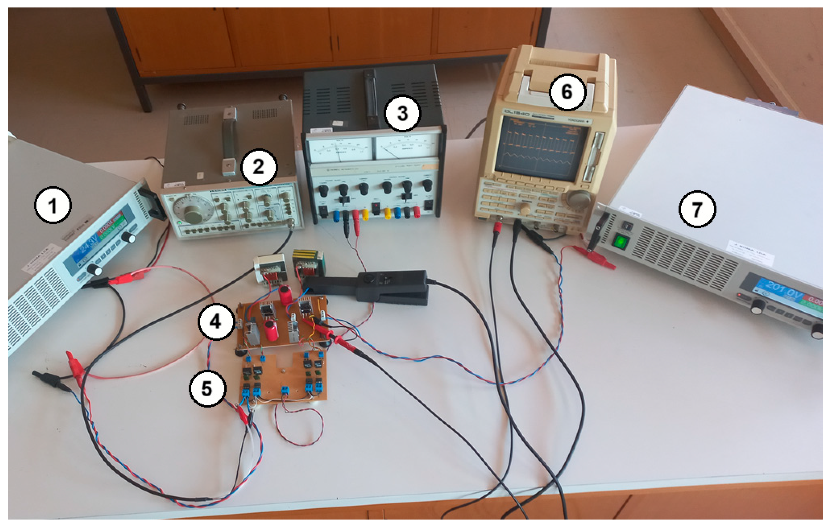
To experimentally verify the performance of the proposed bidirectional DC-DC converter, a laboratory prototype with 1 kW based on the topology presented in Figure 1 was developed and tested. From the low voltage side, this DC-DC converter was supplied with an initial voltage of 24 VDC. From the high-voltage side, this DC-DC converter was connected to DC Electronic Load with Inverter Function (EA-ELR 10200-25 2U 1500 W). Figure 14 shows the experimental test bench with the proposed laboratory prototype, where the most relevant equipment is identified. In this figure, it is possible to see: 1—controlled voltage sources (EA PS8360-30 2U); 2—waveform generator for the proposed bidirectional DC-DC converter; 3—auxiliary power source for the gate drive circuits; 4—proposed DC-DC converter topology using SiC MOSFETs (UJ4SC075006K4S–Onsemi manufacturer); 5—gate drive circuits and protections based on UCC21520 circuit; 6—DL1540 Yokogawa oscilloscope; and 7—DC Electronic Load with Inverter Function (EA-ELR 10200-25 2U 1500 W).
Several experimental tests under operating conditions analogous to the simulated ones proposed in the previous section were also performed in a laboratory environment. A laboratory prototype of the proposed bidirectional Buck-Boost DC-DC converter was implemented and used for this purpose. Table 3 shows the parameters and details of the converter components as well as the operation specifications.
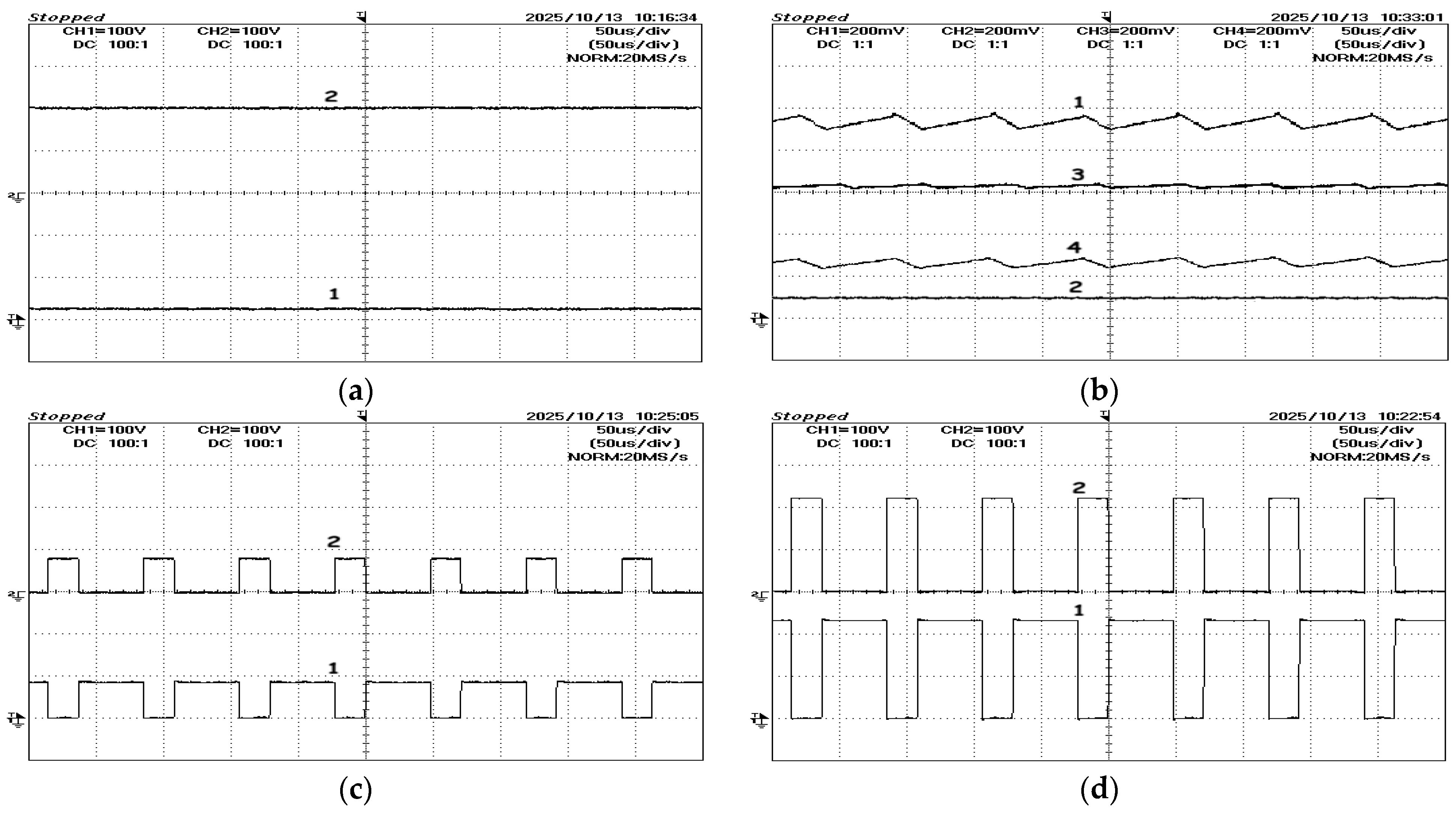
The proposed bidirectional Buck-Boost DC-DC converter laboratory prototype was tested as close as possible to the simulation tests to validate the theoretical considerations. Thus, the first experimental test was also conducted in forward energy transfer mode. For this test, a duty cycle of 0.67 was used for transistors T1 and T2. The corresponding obtained oscilloscope waveforms can be seen in Figure 15. The voltage gains of each channel and time base are described in each figure caption. Figure 15a illustrates the input (Ch1) and output voltages (Ch2) showing agreement with the converter parameters and duty cycle of the transistors T1 and T2, in accordance with the voltage gain ratio given by Equation (5). The input (Ch1) and output currents (Ch2) as well as the current in the inductors (IL1 in Ch3 and IL2 in Ch4) are represented in Figure 15b illustrating continuous waveforms in all the currents. It is also possible to confirm that T1 and T2 operate synchronously, as the transistor voltage waveforms illustrate, namely VT1 in Ch2 of Figure 15c and VT2 in Ch2 of Figure 15d. The transistors T1 and T2 voltage waveforms also confirm that the transistor T2 must withstand the maximum output voltage, while transistor T1 must withstand a much lower voltage, as expected by the theoretical considerations and simulation results.
In DC-DC converters, attention should be addressed to the ripple in the inductors. Excessive ripple can affect the core losses in the inductors (high ripple current means the magnetic flux swings more widely each cycle, thus core losses (hysteresis + eddy currents) increase roughly with both frequency and ΔB (proportional to ΔIL) and conduction losses in capacitors (due to ESR) and power devices. The switching losses of power devices can also degrade the efficiency of the DC-DC power converter due to higher currents or voltages/overvoltages during the turn-on and turn-off process. On the other hand, to reduce the ripple, it is necessary to increase the switching frequency of the power devices, maintaining the same current average value. This will reduce the conduction losses of power devices but increase their switching losses inversely. The same goes for core losses. Reducing the higher current is important to reduce core losses but increasing the frequency creates an opposite effect. Since we cannot escape from power losses, the best we can do is to balance the parameters and operation of the converter to obtain acceptable efficiency and proper operation. In the design of the proposed converter, a ripple from 10 to 15% (which happens in the current of L2) was considered acceptable as it happens with most converters of this type.
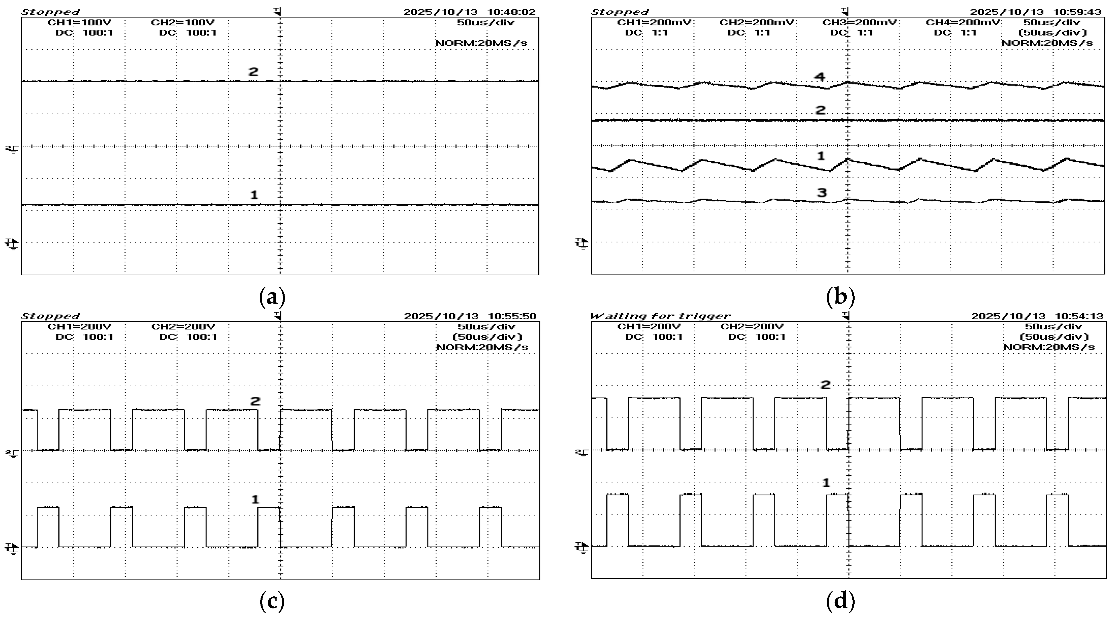
Like the simulation results, several experiments tests with the proposed bidirectional Buck-Boost DC-DC converter prototype operating in forward energy transfer mode and Buck operation were also performed, using again the parameters listed in Table 3. Figure 16 shows the oscilloscope waveforms obtained in steady state and with a duty cycle of 0.2. Analyzing the converter from the input (Vi) (see Ch2 in Figure 16a) to the output (Vo) (see Ch1 in Figure 16a), a high-voltage gain reduction can be noticed in this condition, confirming the Buck operation in forward energy transfer mode. The current injected into the output voltage source (see Ch2 in Figure 16b) provided by the input voltage source (Ch1 in Figure 16b) and the currents in the inductors (IL1 as Ch3 in Figure 16b and IL2 as Ch4 in Figure 16b) are consistent with the simulation results and all of them remain continuous. In this condition, the transistors T1 and T2 are used to transfer energy and the blocking voltages in transistors T1 and T2 are presented in Figure 16c-Ch2 and Figure 16d-Ch2, respectively. Similarly, these figures show that transistor T1 needs to withstand a lower voltage, while transistor T2 needs to withstand a higher voltage, namely the capacitor C1 voltage. Again, the voltage gains of each channel and time base are described in each figure caption.
Experimental results with the proposed bidirectional Buck-Boost DC-DC converter operating in reverse energy transfer mode were also performed. Figure 17 shows the waveforms obtained for these experimental tests in steady state and with a duty cycle of 0.33. When seen from the converter output (Vo) side (see Ch2 in Figure 17a) to the input (Vi) side (see Ch1 in Figure 17a), a high-voltage gain reduction is noticed. In this situation, the current injected into the input voltage source (see Ch1 in Figure 17b) remains continuous, indicating that this converter is suitable for battery applications or other applications requiring continuous currents. The current at the output terminals (see Ch2 in Figure 17b) is also continuous, as well as the currents in the inductors L1 (see Ch3 in Figure 17b) and L2 (see Ch4 in Figure 17b). The inversion of the currents presented in Figure 17b checks the reverse energy transfer mode. The blocking voltages in transistors T3 and T4 are also visible, showing that transistor T3 (see Ch1 in Figure 17c) needs to withstand a lower voltage, while transistor T4 (see Ch1 in Figure 17d) needs to withstand a higher voltage, namely the capacitor C1 voltage (see Ch2 in Figure 17e). The voltage waveforms in all the transistors and capacitors are available from Figure 17c–e.
Another experimental test to confirm the Boost operation of this converter in reverse energy transfer mode, was also performed. Figure 18 shows the results in this situation in which the duty cycle is 0.67. From this figure, it is possible to see that, in contrast to the previous test, the circuit now operates in Boost mode since the input voltage (see Ch2 in Figure 18a) is higher than the output voltage (see Ch1 in Figure 18a). The remaining waveforms are like the previous experimental test, where the inversion of the currents with different average values can be seen again due to the Boost operation (Figure 18b). Figure 18c,d present the blocking voltages in all the transistors, showing that transistor T3 (see Ch1 in Figure 18c) needs to withstand a lower voltage, while transistor T4 (see Ch1 in Figure 18d) needs to withstand a higher voltage, namely the capacitor C1 voltage (see Ch2 in Figure 18e).
In addition, the proposed bidirectional Buck-Boost DC-DC converter was also experimentally tested in several transient conditions. Similarly to the simulation results, these experimental tests were performed with the converter operating in forward and reverse energy transfer mode, where step changes in the duty cycle were considered, specifically from 0 to 0.4, 0.5, 0.6, and ending at 0.45. The resulting waveforms of this test can be seen in the next figure, confirming the changes in the output voltages (see Ch2 in Figure 19a), and the variation in both input (see Ch2 in Figure 19b) and output (see Ch1 in Figure 19b) currents because of these duty cycle variation steps. This figure also confirms the intended input and output continuous currents. They also change their value in response to step changes in the duty cycle while remaining without discontinuities. Similarly, the proposed bidirectional Buck-Boost DC-DC converter prototype was also subjected to transient tests also in the reverse energy transfer mode. Again, step changes in the duty cycle were considered, ranging from 0 to 0.4, 0.5, 0.6, ending at 0.45. Figure 20 shows the obtained experimental waveforms in such conditions. In this mode, only the input voltage changes in response to the duty cycle variation. When compared to the previous test, the input and output currents in this figure reverse their direction, confirming the reverse energy flow. These currents are continuous in all operating regions. Such voltage variations were made thanks to the analog remote control interface available in the power sources of the laboratory.
Finally, some experimental tests in transient mode were also conducted by applying step changes to the input voltage source (Vi) during the forward-mode operation and step changes to the output voltage source (Vo) during reverse-mode operation. Figure 21a presents the obtained results for the input and output voltages for the forward-mode operation test with a duty cycle of 0.4, considering multiple step input voltage changes. Similarly, Figure 21b presents the obtained results for the input and output voltages for the reverse-mode operation test with a duty cycle of 0.45, considering multiple step output voltage changes, which is the reverse condition. As verified in the previous case, there are also some transient oscillations immediately after the step changes in the input or output voltage source. These oscillations are the natural consequence of the parameters of the components adopted in these experimental tests. Despite not being performed in this prototype version, some optimizations can be performed if necessary to mitigate these oscillations and overvoltages.
7. Conclusions

This work is focused on the analysis and design of a new topology for a bidirectional Buck-Boost 2L2C DC-DC converter. This converter shows a feature not typically found in previous topologies, namely the ability to provide Buck-Boost in both power flow directions. Other distinguishing characteristics of this converter include its high static voltage gain ratio and the ability to sustain continuous input and output currents. The proposed converter has a simple structure as well, and it only requires four transistors with antiparallel diodes, two inductors, and two capacitors. This work addressed several issues, including theoretical analysis and design guidelines. Additionally, the work also included building an experimental prototype to verify the theoretical assumptions and converter component design. Using steady state and transient conditions with step variations in the duty cycle, experimental results confirmed the continuous input and output currents, the high input-output static Buck-Boost gain in forward and reverse power transfer, and fast response to transient step variations in the duty cycle.

Author Contributions

Conceptualization, V.F.P., A.C. and D.F.; methodology, V.F.P. and J.F.S.; formal analysis, V.F.P. and J.F.S.; investigation, V.F.P., A.C., D.F. and T.A.; resources, A.C., D.F. and T.A.; writing—original draft, V.F.P. and A.C.; writing—review and editing, D.F., T.A. and J.F.S.; visualization, V.F.P., A.C., D.F., T.A. and J.F.S.; supervision, V.F.P. and J.F.S.; project administration, D.F. and T.A.; funding acquisition, A.C. and D.F. All authors have read and agreed to the published version of the manuscript.

Funding

This research was supported by national funds through FCT Fundação para a Ciência e a Tecnologia with reference UIDB/50021/2020 and CTS/00066.

Data Availability Statement

The original contributions presented in this study are included in the article. Further inquiries can be directed to the corresponding author.

Conflicts of Interest

The authors declare no conflicts of interest.

References

  1. Souza Junior, M.E.T.; Freitas, L.C.G. Power Electronics for Modern Sustainable Power Systems: Distributed Generation, Microgrids and Smart Grids—A Review. Sustainability 2022, 14, 3597. [Google Scholar] [CrossRef]
  2. Quinn, C.A.; Dalal, D.B. Empowering the electronics industry: A power technology roadmap. CPSS Trans. Power Electron. Appl. 2017, 2, 306–319. [Google Scholar] [CrossRef]
  3. Shibata, P.; Ramoul, J.; Rodriguez, R.; Callegaro, A.D.; Suntharalingam, P.; Cotton, J.S.; Emadi, A. Weight Reduction Considerations for Thermal Management of Aerospace Power Electronics. In Proceedings of the 2021 IEEE Transportation Electrification Conference & Expo (ITEC), Chicago, IL, USA, 21–25 June 2021; pp. 502–506. [Google Scholar] [CrossRef]
  4. ElMenshawy, M.; Massoud, A. Medium-Voltage DC-DC Converter Topologies for Electric Bus Fast Charging Stations: State-of-the-Art Review. Energies 2022, 15, 5487. [Google Scholar] [CrossRef]
  5. Coelho, S.; Monteiro, V.; Afonso, J.L. Topological Advances in Isolated DC–DC Converters: High-Efficiency Design for Renewable Energy Integration. Sustainability 2025, 17, 2336. [Google Scholar] [CrossRef]
  6. Dominguez, M.; Fernández-Cardador, A.; Cucala, A.P.; Pecharroman, R.R. Energy Savings in Metropolitan Railway Substations Through Regenerative Energy Recovery and Optimal Design of ATO Speed Profiles. IEEE Trans. Autom. Sci. Eng. 2012, 9, 496–504. [Google Scholar] [CrossRef]
  7. Ramsey, D.; Letrouve, T.; Bouscayrol, A.; Delarue, P. Comparison of Energy Recovery Solutions on a Suburban DC Railway System. IEEE Trans. Transp. Electrif. 2021, 7, 1849–1857. [Google Scholar] [CrossRef]
  8. Peña, D.; Arevalo, P.; Ortiz, Y.; Jurado, F. Survey of Optimization Techniques for Microgrids Using High-Efficiency Converters. Energies 2024, 17, 3657. [Google Scholar] [CrossRef]
  9. Eajal, A.A.; Muda, H.; Aderibole, A.; Hosani, M.A.; Zeineldin, H.; El-Saadany, E.F. Stability Evaluation of AC/DC Hybrid Microgrids Considering Bidirectional Power Flow Through the Interlinking Converters. IEEE Access 2021, 9, 43876–43888. [Google Scholar] [CrossRef]
  10. Korompili, A.; Monti, A. Review of Modern Control Technologies for Voltage Regulation in DC/DC Converters of DC Microgrids. Energies 2023, 16, 4563. [Google Scholar] [CrossRef]
  11. Meng, F.; Yang, W.; Yang, S.; Gao, L. Active Harmonic Reduction for 12-Pulse Diode Bridge Rectifier at DC Side with Two-Stage Auxiliary Circuit. IEEE Trans. Ind. Inform. 2015, 11, 64–73. [Google Scholar] [CrossRef]
  12. Castañeda-Rubalcaba, D.G.; Sosa, J.M.; Vázquez-Guzmán, G.; Martinez-Rodriguez, P.R. Brief Overview on Non-Isolated DC-DC Bidirectional Power Converter Topologies. In Proceedings of the 2023 IEEE International Autumn Meeting on Power, Electronics and Computing (ROPEC), Ixtapa, Mexico, 18–20 October 2023; pp. 1–6. [Google Scholar] [CrossRef]
  13. Gorji, S.A.; Sahebi, H.G.; Ektesabi, M.; Rad, A.B. Topologies and Control Schemes of Bidirectional DC–DC Power Converters: An Overview. IEEE Access 2019, 7, 117997–118019. [Google Scholar] [CrossRef]
  14. Wang, Z.; Su, X.; Zeng, N.; Jiang, J. Overview of Isolated Bidirectional DC–DC Converter Topology and Switching Strategies for Electric Vehicle Applications. Energies 2024, 17, 2434. [Google Scholar] [CrossRef]
  15. Tong, Y.; Salhi, I.; Wang, Q.; Lu, G.; Wu, S. Bidirectional DC-DC Converter Topologies for Hybrid Energy Storage Systems in Electric Vehicles: A Comprehensive Review. Energies 2025, 18, 2312. [Google Scholar] [CrossRef]
  16. Hong, S.-Y.; Ryu, S.-G.; Park, C.-B.; Lee, H.-W.; Lee, J.-B. Two-Stage Isolated Bidirectional DC-DC Converter with Low Profile and Double Heat Sink for Battery Charging/Discharging System. Electronics 2025, 14, 283. [Google Scholar] [CrossRef]
  17. Goyal, V.K.; Shukla, A. Two-Stage Hybrid Isolated DC–DC Boost Converter for High Power and Wide Input Voltage Range Applications. IEEE Trans. Ind. Electron. 2022, 69, 6751–6763. [Google Scholar] [CrossRef]
  18. Yu, K.; Zhuo, F.; Wang, F.; Zhu, T.; Gou, Y. Adaptive Deep-Learning-Based Steady-State Modeling and Fast Control Strategy for CLLC DC-DC Converter in Highly Renewable Penetrated System. IEEE J. Emerg. Sel. Top. Circuits Syst. 2022, 12, 205–219. [Google Scholar] [CrossRef]
  19. Yoo, K.M.; Lee, J.Y. A 10-kW Two-Stage Isolated/Bidirectional DC/DC Converter with Hybrid-Switching Technique. IEEE Trans. Ind. Electron. 2013, 60, 2205–2213. [Google Scholar] [CrossRef]
  20. Ma, H.; Lei, J.; Qin, G.; Guo, Z.; Hao, C. Efficiency Optimization Control Strategies for High-Voltage-Ratio Dual-Active-Bridge (DAB) Converters in Battery Energy Storage Systems. Energies 2025, 18, 2650. [Google Scholar] [CrossRef]
  21. Serban, E.; Pondiche, C.; Ordonez, M. Analysis and Design of Bidirectional Parallel-Series DAB-Based Converter. IEEE Trans. Power Electron. 2023, 38, 10370–10382. [Google Scholar] [CrossRef]
  22. Liu, C.; Xu, C.; Bao, Y.; Chen, H.; Chen, X.; Chen, M.; Jiang, F.; Liang, Z. Off-Grid Smoothing Control Strategy for Dual Active Bridge Energy Storage System Based on Voltage Droop Control. Energies 2025, 18, 1585. [Google Scholar] [CrossRef]
  23. Ataullah, H.; Iqbal, T.; Khalil, I.U.; Ali, U.; Blazek, V.; Prokop, L.; Ullah, N. Analysis of the Dual Active Bridge-Based DC-DC Converter Topologies, High-Frequency Transformer, and Control Techniques. Energies 2022, 15, 8944. [Google Scholar] [CrossRef]
  24. Majumder, P.; Kapat, S.; Kastha, D.; Patel, A. Modeling, Analysis, and Design of 48/12V Digitally Controlled Non-Isolated DAB-Type Converters for Automotive and Data Center Applications. In Proceedings of the 2023 IEEE International Conference on Power Electronics, Smart Grid, and Renewable Energy (PESGRE), Trivandrum, India, 17–20 December 2023; pp. 1–6. [Google Scholar] [CrossRef]
  25. Swaminathan, N.; Cao, Y. An Overview of High-Conversion High-Voltage DC–DC Converters for Electrified Aviation Power Distribution System. IEEE Trans. Transp. Electrif. 2020, 6, 1740–1754. [Google Scholar] [CrossRef]
  26. Sato, Y.; Uno, M.; Nagata, H. Nonisolated Multiport Converters Based on Integration of PWM Converter and Phase-Shift-Switched Capacitor Converter. IEEE Trans. Power Electron. 2020, 35, 455–470. [Google Scholar] [CrossRef]
  27. Sarani, S.; Liang, X. Design Criteria of Non-Isolated Bidirectional DC-DC Converters: A Review. IEEE Trans. Ind. Appl. 2025, 61, 8771–8798. [Google Scholar] [CrossRef]
  28. Singh, A.K.; Mishra, A.K.; Gupta, K.K.; Siwakoti, Y.P. High Voltage Gain Bidirectional DC-DC Converters for Supercapacitor Assisted Electric Vehicles: A Review. CPSS Trans. Power Electr. Appl. 2022, 7, 386–398. [Google Scholar] [CrossRef]
  29. Mumtaz, F.; Yahaya, N.Z.; Meraj, S.T.; Singh, B.; Kannan, R.; Ibrahim, O. Review on non-isolated DC-DC converters and their control techniques for renewable energy applications. Shams Eng. J. 2021, 12, 3747–3763. [Google Scholar] [CrossRef]
  30. Lopes, W.F.; Martins, M.L.d.S.; Converti, A.; Siqueira, H.V.; Illa Font, C.H. Experimental Evaluation of a 2 kW/100 kHz DC–DC Bidirectional Converter Based on a Cuk Converter Using a Voltage-Doubler Concept. Energies 2024, 17, 362. [Google Scholar] [CrossRef]
  31. Ye, Y.; Chen, M.; Wang, X.; Cao, L. Boost-type common-ground PV inverter based on quasi-Z-source and switched-capacitor. Int. J. Electr. Power Energy Syst. 2023, 144, 108522. [Google Scholar] [CrossRef]
  32. Zhang, Y.; Liu, Q.; Gao, Y.; Li, J.; Sumner, M. Hybrid Switched-Capacitor/Switched-Quasi-Z-Source Bidirectional DC–DC Converter with a Wide Voltage Gain Range for Hybrid Energy Sources EVs. IEEE Trans. Ind. Electron. 2019, 66, 2680–2690. [Google Scholar] [CrossRef]
  33. Zhang, Y.; Gao, Y.; Zhou, L.; Sumner, M. A switched-capacitor bidirectional DC-DC converter with wide voltage gain range for electric vehicles with Hybrid Energy Sources. IEEE Trans. Power Electron. 2018, 33, 9459–9469. [Google Scholar] [CrossRef]
  34. Sano, K.; Fujita, H. Performance of a high-efficiency switched capacitor-based resonant converter with phase-shift control. IEEE Trans. Power Electron. 2021, 26, 344–354. [Google Scholar] [CrossRef]
  35. Santra, S.B.; Chatterjee, D.; Siwakoti, Y.P. Coupled Inductor Based Soft Switched High Gain Bidirectional DC-DC Converter with Reduced Input Current Ripple. IEEE Trans. Ind. Electron. 2023, 70, 1431–1443. [Google Scholar] [CrossRef]
  36. Cornea, O.; Andreescu, G.D.; Muntean, N.; Hulea, D. Bidirectional Power Flow Control in a DC Microgrid Through a Switched-Capacitor Cell Hybrid DC–DC Converter. IEEE Trans. Ind. Electron. 2017, 64, 3012–3022. [Google Scholar] [CrossRef]
  37. Wu, H.; Sun, K.; Chen, L.; Zhu, L.; Xing, Y. High Step-Up/Step-Down Soft-Switching Bidirectional DC–DC Converter with Coupled Inductor and Voltage Matching Control for Energy Storage Systems. IEEE Trans. Ind. Electron. 2016, 63, 2892–2903. [Google Scholar] [CrossRef]
  38. Ahmad, A.; Reza, M.M.; Beig, A.R.; Alsawalhi, J.Y.; Jaafari, K.A. High Voltage Gain Switched-Z-Source Bidirectional DC-DC Converter. IEEE Access 2022, 10, 53560–53577. [Google Scholar] [CrossRef]
  39. Ardi, H.; Ajami, A.; Kardan, F.; Avilagh, S.N. Analysis and Implementation of a Non-isolated Bidirectional DC–DC Converter with High Voltage Gain. IEEE Trans. Ind. Electron. 2016, 63, 4878–4888. [Google Scholar] [CrossRef]
  40. Yang, J.W.; Do, H.L. Soft-Switching Bidirectional DC-DC Converter Using a Lossless Active Snubber. IEEE Trans. Circuits Syst. I Regul. Pap. 2014, 61, 1588–1596. [Google Scholar] [CrossRef]
  41. Pires, V.F.; Foito, D.; Cordeiro, A. A DC–DC Converter with Quadratic Gain and Bidirectional Capability for Batteries/Supercapacitors. IEEE Trans. Ind. Appl. 2018, 54, 274–285. [Google Scholar] [CrossRef]
  42. Hosseini, S.H.; Ghazi, R.; Heydari-Doostabad, H. An Extendable Quadratic Bidirectional DC–DC Converter for V2G and G2V Applications. IEEE Trans. Ind. Electron. 2021, 68, 4859–4869. [Google Scholar] [CrossRef]
  43. Jiang, F.; Wang, P.; Wang, Z.; Deng, Q.; Li, B.; Tao, L.; Cheng, Z. A Zero Current Ripple Bidirectional DC–DC Converter with High Voltage Gain and Common Ground for Hybrid Energy Storage System EVs. IEEE J. Emerg. Sel. Top. Power Electron. 2023, 11, 4882–4894. [Google Scholar] [CrossRef]
  44. Pires, V.F.; Cordeiro, A.; Foito, D.; Pires, A.J. Bidirectional DC-DC Converter with High Voltage Step-up/down Ratio for The Interconnection of Unipolar and Bipolar DC Microgrids. In Proceedings of the 12th International Conference on Smart Grid (icSmartGrid), Setubal, Portugal, 27–29 May 2024; pp. 54–59. [Google Scholar] [CrossRef]
  45. Gray, P.A.; Lehn, P.W.; Yakop, N. A Modular Multilevel DC–DC Converter with Flying Capacitor Converter Like Properties. IEEE Trans. Ind. Electron. 2022, 69, 6774–6783. [Google Scholar] [CrossRef]
  46. Abdulslam, A.; Mohammad, B.; Ismail, M.; Mercier, P.P.; Ismail, Y. A 93% Peak Efficiency Fully-Integrated Multilevel Multistate Hybrid DC–DC Converter. IEEE Trans. Circuits Syst. I Regul. Pap. 2018, 65, 2617–2630. [Google Scholar] [CrossRef]
  47. Wang, B.; Zhang, X.; Manandhar, U.; Gooi, H.B.; Liu, Y.; Tan, X. Bidirectional Three-Level Cascaded Converter with Deadbeat Control for HESS in Solar-Assisted Electric Vehicles. IEEE Trans. Transp. Electrif. 2019, 5, 1190–1201. [Google Scholar] [CrossRef]
  48. Erikson, R.; Maksimovic, D. Fundamenals of Power Electronics; Springer: Berlin/Heidelberg, Germany, 2020; p. 1084. [Google Scholar]
Figure 1. Topology of the proposed bidirectional Buck-Boost DC-DC converter with a wide voltage gain range.
Energies 19 00043 g001
Figure 2. CCM operating modes of the proposed bidirectional Buck-Boost DC-DC converter in forward energy transfer mode: (a) Mode 1; (b) Mode 2.
Energies 19 00043 g002
Figure 3. Static voltage gain versus duty cycle of the conventional bidirectional Buck-Boost converter with the proposed bidirectional Buck-Boost quadratic converter in both directions (considering the forward energy transfer operation).
Energies 19 00043 g003
Figure 4. CCM operating modes of the proposed bidirectional Buck-Boost DC-DC converter in reverse energy transfer mode: (a) Mode 1; (b) Mode 2.
Energies 19 00043 g004
Figure 5. Static voltage gain versus duty cycle of the conventional bidirectional Buck-Boost converter with the proposed bidirectional Buck-Boost quadratic converter in both directions (considering reverse energy transfer operation).
Energies 19 00043 g005
Figure 6. Static voltage gain versus duty cycle comparison for the proposed and similar bidirectional buck-boost converters; (a) considering forward energy transfer operation; (b) considering reverse energy transfer operation [28,29,31,32,35].
Energies 19 00043 g006
Figure 7. Waveforms obtained from simulation tests for the bidirectional Buck-Boost DC-DC converter operating in forward energy transfer mode and in Boost condition; (a) input and output voltages; (b) input and output currents and inductor currents; (c) voltages over transistors T1 and T3; (d) voltages over transistors T2 and T4; (e) currents through transistors T1 and T2; (f) currents through transistors T3 and T4; (g) capacitor voltages.
Energies 19 00043 g007
Figure 8. Waveforms obtained from simulation tests for the bidirectional Buck-Boost DC-DC converter operating in forward energy transfer mode and in Buck condition (a) input and output voltages; (b) input and output currents and inductor currents; (c) voltages over transistors T1 and T3; (d) voltages over transistors T2 and T4; (e) currents through transistors T1 and T2; (f) currents through transistors T3 and T4; (g) capacitor voltages.
Energies 19 00043 g008
Figure 9. Waveforms obtained from simulation tests for the bidirectional Buck-Boost DC-DC converter operating in reverse energy transfer mode and in Buck condition (a) input and output voltages; (b) input and output currents and inductor currents; (c) voltages over transistors T1 and T3; (d) voltages over transistors T2 and T4; (e) currents through transistors T1 and T2; (f) currents through transistors T3 and T4; (g) capacitor voltages.
Energies 19 00043 g009
Figure 10. Waveforms obtained from simulation tests for the bidirectional Buck-Boost DC-DC converter operating in reverse energy transfer mode and in Boost condition; (a) input and output voltages; (b) input and output currents and inductor currents; (c) voltages over transistors T1 and T3; (d) voltages over transistors T2 and T4; (e) currents through transistors T1 and T2; (f) currents through transistors T3 and T4; (g) capacitor voltages.
Energies 19 00043 g010
Figure 11. Waveforms obtained through simulation tests for the bidirectional Buck-Boost DC-DC converter in transient condition operating in the forward energy transfer mode. Step changes in the duty cycle were considered, ranging from 0 to 0.4, 0.5, 0.6, and ending in 0.45; (a) input and output voltages; (b) input and output currents.
Energies 19 00043 g011
Figure 12. Waveforms obtained through simulation tests for the bidirectional Buck-Boost DC-DC converter under transient conditions while operating in reverse energy transfer mode. Step changes in the duty cycle were considered, ranging from 0 to 0.4, 0.5, 0.6, and ending at 0.45; (a) input and output voltages; (b) input and output currents.
Energies 19 00043 g012
Figure 13. Waveforms obtained through simulation tests for the bidirectional Buck-Boost DC-DC converter under transient conditions with sudden changes in the voltage sources; (a) step changes in the input voltage (Vi) source during forward-mode operation; (b) step changes in the output voltage source (Vo) during reverse-mode operation.
Energies 19 00043 g013
Figure 14. Photograph of the experimental test bench with the proposed laboratorial prototype. In this figure, it is possible to see: 1—controlled voltage sources (EA PS8360-30 2U); 2—waveform generator for the proposed bidirectional DC-DC converter; 3—auxiliary power source for the gate drive circuits; 4—proposed DC-DC converter topology using SiC MOSFETs (UJ4SC075006K4S–Onsemi manufacturer); 5—gate drive circuits and protections based on UCC21520 circuit; 6—DL1540 Yokogawa oscilloscope; 7—DC Electronic Load with Inverter Function (EA-ELR 10200-25 2U 1500 W).
Energies 19 00043 g014
Figure 15. Waveforms obtained through experimental tests for bidirectional Buck-Boost DC-DC converter operating in the forward energy transfer mode; (a) input and output voltages (Channel Gain-Ch1 = Ch2 = 100 V/div; Time division: 50 μs/div); (b) input and output currents and inductor currents (Channel Gain-Ch1 = Ch2 = Ch3 = Ch4 = 200 mV/div, using current probes with 100 mV/A; Time division: 50 μs/div); (c) voltages over transistors T1 and T3 (Channel Gain-Ch1 = Ch2 = 100 V/div; Time division: 50 μs/div); (d) voltages over transistors T2 and T4 (Channel Gain-Ch1 = Ch2 = 100 V/div; Time division: 50 μs/div).
Energies 19 00043 g015
Figure 16. Waveforms obtained through experimental tests for the bidirectional Buck-Boost DC-DC converter operating in the reverse energy transfer mode; (a) input and output voltages (Channel Gain-Ch1 = Ch2 = 100 V/div; Time division: 50 μs/div); (b) input and output currents and inductor currents (Channel Gain-Ch1 = Ch2 = Ch3 = Ch4 = 200 mV/div, using current probes with 100 mV/A; Time division: 50 μs/div); (c) voltages over transistors T1 (Ch2) and T3 (Ch1) (Channel Gain-Ch1 = Ch2 = 200 V/div; Time division: 50 μs/div); (d) voltages over transistors T2 (Ch2) and T4 (Ch1) (Channel Gain-Ch1 = Ch2 = 200 V/div; Time division: 50 μs/div).
Energies 19 00043 g016
Figure 17. Waveforms obtained from simulation tests for the bidirectional Buck-Boost DC-DC converter operating in reverse energy transfer mode and in Buck condition; (a) input and output voltages (Channel Gain-Ch1 = Ch2 = 100 V/div; Time division: 50 μs/div); (b) input and output currents and inductor currents (Channel Gain-Ch1 = Ch2 = Ch3 = Ch4 = 200 mV/div, using current probes with 100 mV/A and Time division: 50 μs/div); (c) voltages over transistors T1 (Ch2) and T3 (Ch1) (Channel Gain-Ch1 = Ch2 = 100 V/div; Time division: 50 μs/div); (d) voltages over transistors T2 (Ch2) and T4 (Ch1) (Channel Gain-Ch1 = Ch2 = 100 V/div; Time division: 50 μs/div); (e) capacitor voltages (Channel Gain-Ch1 = Ch2 = 50 V/div; Time division: 50 μs/div).
Energies 19 00043 g017
Figure 18. Waveforms obtained from simulation tests for the bidirectional Buck-Boost DC-DC converter operating in reverse energy transfer mode and in Buck condition; (a) input and output voltages (Channel Gain-Ch1 = Ch2 = 100 V/div; Time division: 50 μs/div); (b) input and output currents and inductor currents (Channel Gain-Ch1 = Ch2 = Ch3 = Ch4 = 200 mV/div, using current probes with 100 mV/A; Time division: 50 μs/div); (c) voltages over transistors T1 (Ch2) and T3 (Ch1) (Channel Gain-Ch1 = Ch2 = 200 V/div; Time division: 50 μs/div); (d) voltages over transistors T2 (Ch2) and T4 (Ch1) (Channel Gain-Ch1 = Ch2 = 200 V/div; Time division: 50 μs/div); (e) capacitor voltages (Channel Gain-Ch1 = Ch2 = 100 V/div; Time division: 50 μs/div).
Energies 19 00043 g018
Figure 19. Waveforms obtained through experimental tests for the proposed bidirectional Buck-Boost DC-DC converter in transient condition operating in the forward energy transfer mode. Step changes in the duty cycle were considered, ranging from 0 to 0.4, 0.5, 0.6, ending at 0.45; (a) input and output voltages (Channel Gain-Ch1 = Ch2 = 50 V/div; time division: 500 μs/div); (b) input and output currents (Channel Gain-Ch1 = Ch2 = 200 mV/div using current probes with 100 mV/A; time division: 500 μs/div).
Energies 19 00043 g019
Figure 20. Waveforms obtained through experimental tests for the proposed bidirectional Buck-Boost DC-DC converter in transient condition operating in the reverse energy transfer mode. Step changes in the duty cycle were considered, ranging from 0 to 0.4, 0.5, 0.6, and ending at 0.45; (a) input and output voltages (Channel Gain-Ch1 = Ch2 = 50 V/div; Time division: 500 μs/div); (b) input and output currents (Channel Gain-Ch1 = Ch2 = 1 V/div, using current probes with 100 mV/A; time division: 500 μs/div).
Energies 19 00043 g020
Figure 21. Waveforms obtained through experimental tests for the proposed bidirectional Buck-Boost DC-DC converter under transient conditions with step changes in the voltage sources; (a) step changes in the input voltage source (Vi) during forward-mode operation (Channel Gain-Ch1 = Ch2 = 50 V/div; Time division: 500 μs/div); (b) step changes in the output voltage source (Vo) during reverse-mode operation (Channel Gain-Ch1 = Ch2 = 50 V/div; Time division: 500 μs/div).
Energies 19 00043 g021
Table 1. Comparison of the proposed bidirectional Buck-Boost DC-DC converter with similar topologies.
Topology[32][33][35][36][39]Proposed
Voltage Gain Forward Transfer 2 + δ i o 1 δ i o 2 1 δ i o 2 N S N P + 2 1 δ i o 1 + δ i o 1 δ i o 1 1 δ i o 2 δ i o 2 δ i o 1 δ i o 2  
Voltage Gain Reverse Transfer δ i o 3 δ i o δ i o 2 δ i o 2 V o u t δ o i 2 δ o i   δ o i 2 δ o i 2 1 δ o i 1 + δ o i  
Maximum Voltage Stress Over Switches 2 + δ i o V o u t δ i o 2 V o u t δ i o 2 V o u t V i n V o u t 2 V i n V o u t + V o u t V i n + V o u t
Maximum Current Stress Over Switches 1 + 2 δ i o δ i o 1 δ i o 1 + δ o i 2 1 δ o i I i n   2 + N S N P + δ o i 2 + 2 N S N P δ o i I i n   2 V o u t 1 δ i o R L V i n V o u t P o V L + V o u t V i n 2 L 2 f s 1 δ o i δ o i 2 I o u t
Control ComplexityMediumLowHighMediumLowLow
Switches445344
Capacitors422222
Inductors313222
Coupled Inductorsnonoyesnonono
Table 2. Parameters of the converter components and operation specifications.
ParameterValue
Output voltage (Vo)200 V
Input voltage (Vi)24 V
Inductor (L1)5 mH
Inductor (L2)5 mH
Capacitor (C1)1000 µF
Capacitor (C2)1000 µF
Switching frequency (fPWM)14 kHz
Table 3. Parameters and details of the converter components and operational specifications.
ParameterValue
Output voltage (Vo)200 V
Input voltage (Vi)24 V
Inductor (L1)5 mH
Inductor (L2)5 mH
Copper WireLitz 0.08 SE F155 G1
Ferrite Core for InductorsE70/33/32DG TDK with core type N87
Capacitor (C1)Kemet 1000 µF/250 V(ESR = 126 mΩ)
Capacitor (C2)Kemet 1000 µF/250 V(ESR = 126 mΩ)
Switching Frequency (fPWM)14 kHz
Power DevicesUJ4SC075006K4S
Disclaimer/Publisher’s Note: The statements, opinions and data contained in all publications are solely those of the individual author(s) and contributor(s) and not of MDPI and/or the editor(s). MDPI and/or the editor(s) disclaim responsibility for any injury to people or property resulting from any ideas, methods, instructions or products referred to in the content.