1. Introduction
As electronic devices continue to evolve toward miniaturization and a higher integration density, traditional planar transistors are reaching their physical and performance limitations. Vertical thin-film transistors (VTFTs) have emerged as a promising alternative through their adoption of a vertical architecture, which significantly reduces the device footprint. VTFTs can be seamlessly integrated with a wide range of functional components, including sensors, memory units, and light-emitting diodes, making them highly suitable for next-generation integrated circuits, advanced display technologies, and multifunctional sensing systems [
1,
2,
3,
4,
5]. This vertical integration architecture offers the potential to greatly enhance the device packing density and system performance.
Indium–gallium–zinc oxide (IGZO), characterized by its high electron mobility, low-temperature fabrication capabilities, and superior performance in large-area production, has emerged as a crucial active layer material for next-generation display drivers [
6,
7]. The integration of IGZO into vertical channel TFTs (VC-IGZO-TFTs) combines the advantages of both material and structure, offering great potential for high-performance applications. Various strategies have been proposed to realize novel VC-IGZO-TFTs and enhance their electronic performance, including atomic layer deposition (ALD), sputtering, solution methods, and so on [
8,
9,
10]. However, these fabrication techniques typically involve complex structural designs requiring photolithography and etching processes, which increase the manufacturing complexity and cost, thereby limiting their scalability and commercial viability.
To overcome these challenges, a simplified vertical device configuration—comprising a gate electrode, gate dielectric, porous source electrode, IGZO channel layer, and drain electrode—has gained attention for its reduced process complexity and integration potential. Within this structure, the porous source electrode plays a crucial role in facilitating the vertical charge injection and significantly influences the overall electrical performance of the device. Various materials, including thin metals, silver nanowires, and carbon nanotubes, have been investigated as porous source materials [
11,
12,
13,
14,
15,
16,
17,
18,
19,
20,
21,
22]. Currently, Mxene, as an emerging two-dimensional material, stands out for its thinness, excellent electrical conductivity, and favorable mechanical properties. However, a systematic analysis of how the concentration of spin-coated MXene influences electrode porosity, sheet resistance, and ultimately the electrical and mechanical performance of VC-TFTs is still lacking.
In this work, a facile and scalable fabrication approach for VC-IGZO-TFTs using spin-coated MXene as a porous source electrode was created. The effects of the MXene concentration on sheet resistance, porosity, and the electrical properties of VC-IGZO-TFTs devices are systematically studied. The electrical reliability under bias stress and the mechanical robustness under various bending conditions are further evaluated. In addition, flexible VC-IGZO-TFTs are fabricated on polyimide (PI) substrates using a low-temperature process, demonstrating the potential of this architecture for high-performance, flexible electronic applications.
2. Materials and Methods
The silicon substrates with a 200 nm thermally grown SiO2 were acquired from Shandong Zhuojing Electronic Technology Co., Ltd. (Shandong, China). Ti3C2 MXene dispersion with a concentration of 5 mg/mL was purchased from the Science Compass Mall (Beijing, China). The ceramic target used for IGZO film deposition, with a composition of In2O3:Ga2O3:ZnO = 1:1:1, a purity of 99.99%, and dimensions of 12.7 cm × 30.5 cm, was provided by Beijing Yao-sheng Materials Technology Co., Ltd. (Beijing, China).
The silicon wafers were laser-cut into 2.4 × 2.4 cm
2 pieces using a HY-JYS300 laser cutter, and served as substrates for device fabrication. To prepare MXene dispersions with concentrations of 2.0, 2.5, 3.0, 3.5, and 4.0 mg/mL, appropriate volumes of the 5 mg/mL stock solution were diluted with deionized (DI) water to a final volume of 1.0 mL. Specifically, 0.40, 0.50, 0.60, 0.70, and 0.80 mL of the stock was mixed with 0.60, 0.50, 0.40, 0.30, and 0.20 mL of DI water, respectively. All solutions were sonicated for 5 min prior to use to ensure homogeneous dispersion. Spin-coating was performed in two steps: an initial spreading step at 500 rpm for 5 s, followed by a uniform coating step at 2000 rpm for 60 s. The resulting films were then thermally annealed at 100 °C for 600 s to remove the remaining solvent and improve film adhesion. Subsequently, IGZO thin films were deposited onto the MXene-coated substrates at an ambient temperature using high-power impulse magnetron sputtering (HiPIMS) (Model SP-122I, Ljuhv, Nantou, Taiwan). Prior to deposition, the chamber was evacuated to a base pressure of 6.7 × 10⁻⁵ Pa. High-purity argon gas (99.999%) was introduced at a constant flow rate of 40 sccm as the sputtering ambient, and the deposition was carried out under an average applied power of 500 W, with the detailed process parameters provided in our previous work [
23]. The IGZO layer is a cuboid with a length and width of 1000 μm and a height of 35 nm. Finally, the aluminum drain and contact source electrode were fabricated via thermal evaporation, with the distance between the two electrodes as 400 μm. The schematic diagram of VC-IGZO-TFTs based on MXene are shown in
Figure 1b. The porous source electrode, formed by stacking MXene layers with uncovered areas representing the pores, is illustrated in
Figure 1a. Due to the shielding effect, the electrons are accumulated in the pore of the source electrode at the interface between the SiO
2 and IGZO, forming a channel to the drain electrode.
The surface morphologies of the MXene films were examined using field-emission scanning electron microscopy (FESEM, Zeiss Sigma 500, Oberkochen, Germany) operated at an accelerating voltage of 15 kV, with a scale bar of 10 μm. Prior to imaging, the SEM system was calibrated using a certified gold-on-carbon resolution standard. Beam alignment, astigmatism correction, and detector gain were subsequently optimized in accordance with the recommended procedures of the manufacturer to ensure high-resolution and artifact-free imaging. For SEM observation, spin-coated MXene samples (2.4 × 2.4 cm) with various concentrations were annealed, then diced into smaller pieces (<0.5 × 0.5 cm) using a silicon wafer cutter. The surface debris was removed using a nitrogen gun to ensure surface cleanliness. As the films exhibited sufficient conductivity, no additional conductive coating was applied. The thickness of the resulting MXene films was measured via atomic force microscopy (AFM, XE7, Park, Suwon, Republic of Korea). The measured thicknesses for the concentrations of 2.0, 2.5, 3.0, 3.5, and 4.0 mg/mL were 4.7, 7.3, 9.2, 10.9, and 12.6 nm, respectively. The sheet resistance of the MXene films was measured using a four-point probe system (Model T200/A2, Ossila, Sheffield, UK). The system was calibrated using a standard silicon wafer with known resistivity, and probe head spacing was verified with a micrometer gauge. The electrical characteristics of the TFTs were evaluated using a semiconductor parameter analyzer (Keithley 4200-SCS, Cleveland, OR, USA). The instrument was regularly calibrated through internal self-check routines and cross-verified using standard reference devices.
3. Results and Discussion
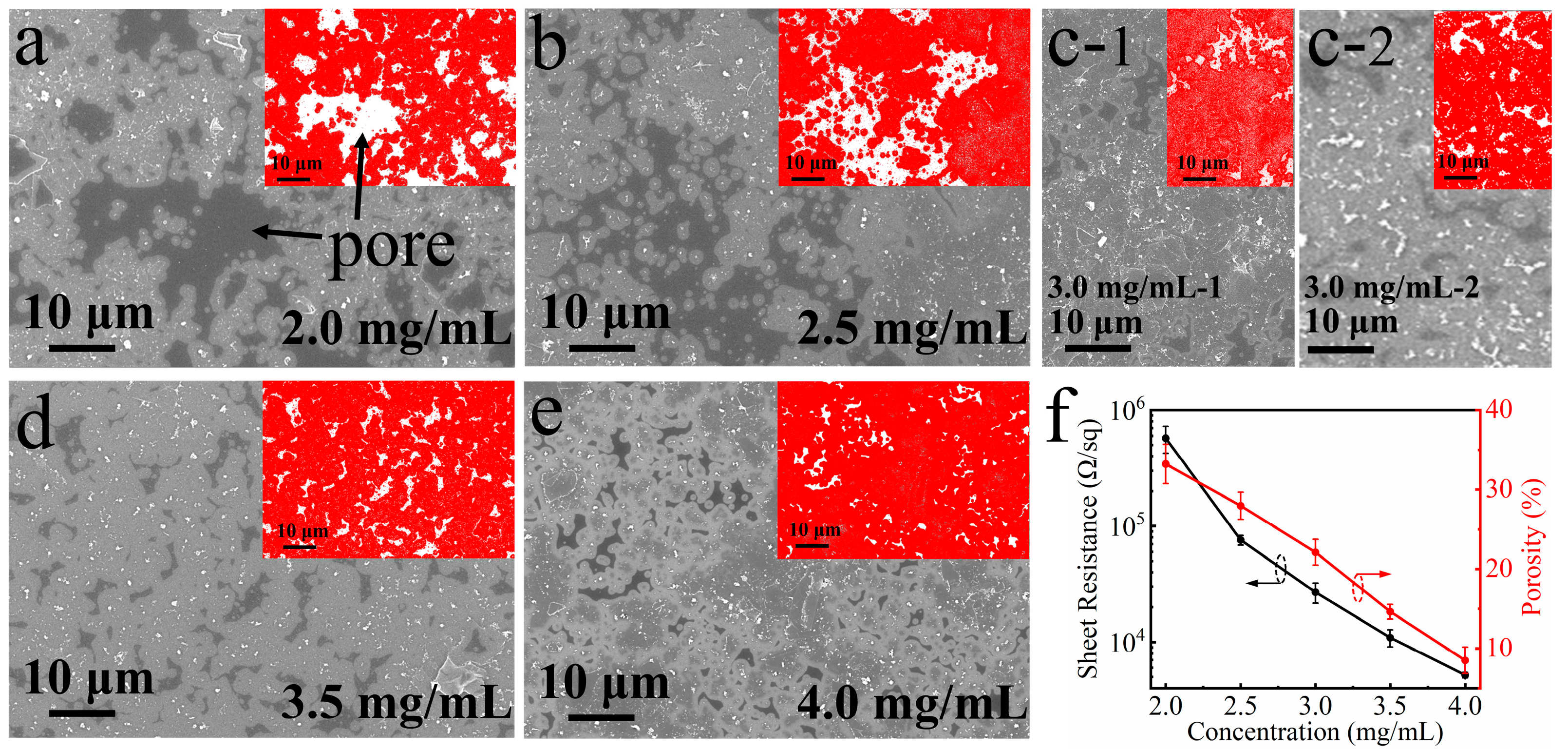
Porosity, defined as the ratio of pore area to total surface area, plays a vital role in governing the performance of vertical channel thin-film transistors (VC-TFTs). However, it presents a trade-off between the electrical conductivity and shielding effects. Higher porosity facilitates the formation of larger current channels through the source electrode due to the presence of numerous and wider pores, but also leads to an increased charge transport path length, resulting in higher sheet resistance. In contrast, lower porosity reduces the overall resistance of the electrode, but limits the number of available electron transmission channels, potentially restricting the carrier injection efficiency. To systematically regulate the porosity of the MXene-based porous source electrode, the concentration of the spin-coated MXene dispersion was varied from 2.0 to 4.0 mg/mL. As shown in the scanning electron microscopy (SEM) images in
Figure 2, distinct changes in the pore morphology are observed with varying concentrations. Notably, SEM imaging in this study was not employed for conventional microstructural analysis, but rather for the quantitative evaluation of surface porosity. In
Figure 2a–e, the lighter regions represent the MXene matrix, while the darker regions correspond to pores. To enhance the visual contrast and facilitate quantitative analysis, the SEM images were processed using ImageJ software (version 1.54f, developed by the National Institutes of Health, Bethesda, MD, USA). Threshold-based image segmentation was performed, in which the pore regions were rendered in white and the MXene framework was highlighted in red, as shown in the figure insets. Porosity was quantitatively determined as the ratio of the white-segmented pore area to the total image area. As the MXene concentration increased from 2.0 to 4.0 mg/mL, the porosity decreased from 32.76% to 8.39%, as shown in
Figure 2f. This trend correlates well with the measured sheet resistance values, which exhibit a significant decrease from 5.47 × 10
5 to 5.38 × 10
3 Ω/sq. The reduced sheet resistance is attributed to enhanced film continuity and improved electrical connectivity between MXene flakes at higher concentrations. This reduction in sheet resistance directly influences the electrical characteristics of the resulting VC-TFTs, leading to an increase in both the off-state current (I
off) and on-state current (I
on), as discussed in the following section. Three independently fabricated samples were prepared for each MXene concentration (2.0, 2.5, 3.0, 3.5, and 4.0 mg/mL) to evaluate the reproducibility of the porosity and sheet resistance measurements. The results showed variations of less than 10% among the three samples at each concentration, as presented in
Figure 2f, demonstrating high uniformity and the excellent reproducibility of the electrode fabrication process. At the optimal concentration of 3.0 mg/mL, two independently prepared electrodes were further characterized. The corresponding SEM images are provided in
Figure 2c-1,c-2. The calculated porosity values for these samples were 22.12% and 23.79%, respectively, indicating minimal batch-to-batch variation. These results confirm the stability and reliability of the spin-coating process for fabricating MXene-based porous source electrodes.
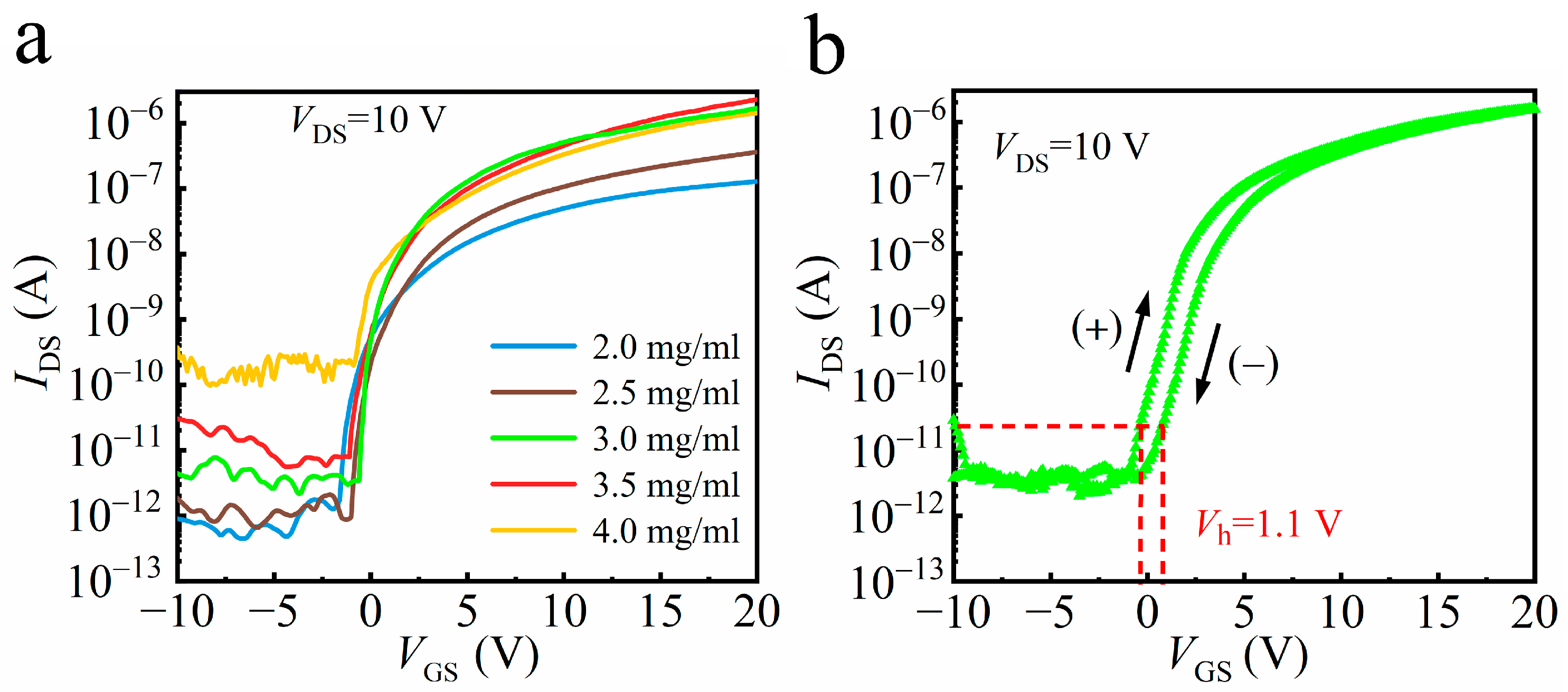
To further validate the impact of the porous source electrode on the device performance, the transfer characteristics of VC-IGZO-TFTs with different MXene concentrations were investigated, as shown in
Figure 3a. As the concentrations increase from 2.0 to 4.0 mg/mL, the key parameters of the VC-IGZO-TFTs are varied. The I
off shows a positive correlation with the MXene concentrations, increasing as the sheet resistance decreases. Meanwhile, the on-off ratio of the current (I
on/I
off) initially increases and then decreases, with values of 7.31 × 10
4, 4.02 × 10
5, 4.90 × 10
5, 2.94 × 10
5, and 4.44 × 10
3 corresponding to MXene concentrations of 2.0, 2.5, 3.0, 3.5, and 4.0 mg/mL, respectively. The threshold voltage (V
th) exhibits a positive shift from −1.14 V to 0.91 V as the MXene concentration increases. The subthreshold swing (SS) remains relatively low across all devices, reaching a minimum of 0.20 V/decade before increasing to 0.64 V/decade at higher concentrations. These trends reflect the combined effects of sheet resistance and porosity, as shown in
Figure 2f. At higher MXene concentrations, the porous source becomes more continuous, resulting in a lower sheet resistance and improved carrier injection, thereby increasing I
off. However, the reduced porosity enhances the shielding effect, which limits the vertical carrier transport, leading to a decrease in I
on and a consequent reduction in the on/off ratio. The enhanced shielding also contributes to the rightward shift in V
th by altering the gate control over the channel. The electrical properties of VC-IGZO-TFTs under different MXene concentrations are summarized in
Table 1. Additionally,
Figure 3b displays the dual-swept transfer characteristics of the VC-IGZO-TFT with a 3 mg/mL MXene source electrode, featuring a hysteresis voltage (V
h = V
reverse-V
forward when I
DS = const.) of 1.1 V. The small hysteresis can be attributed to the vertical transport architecture of the device, which minimizes the influence of the interface trap states commonly observed in planar configurations [
24,
25].
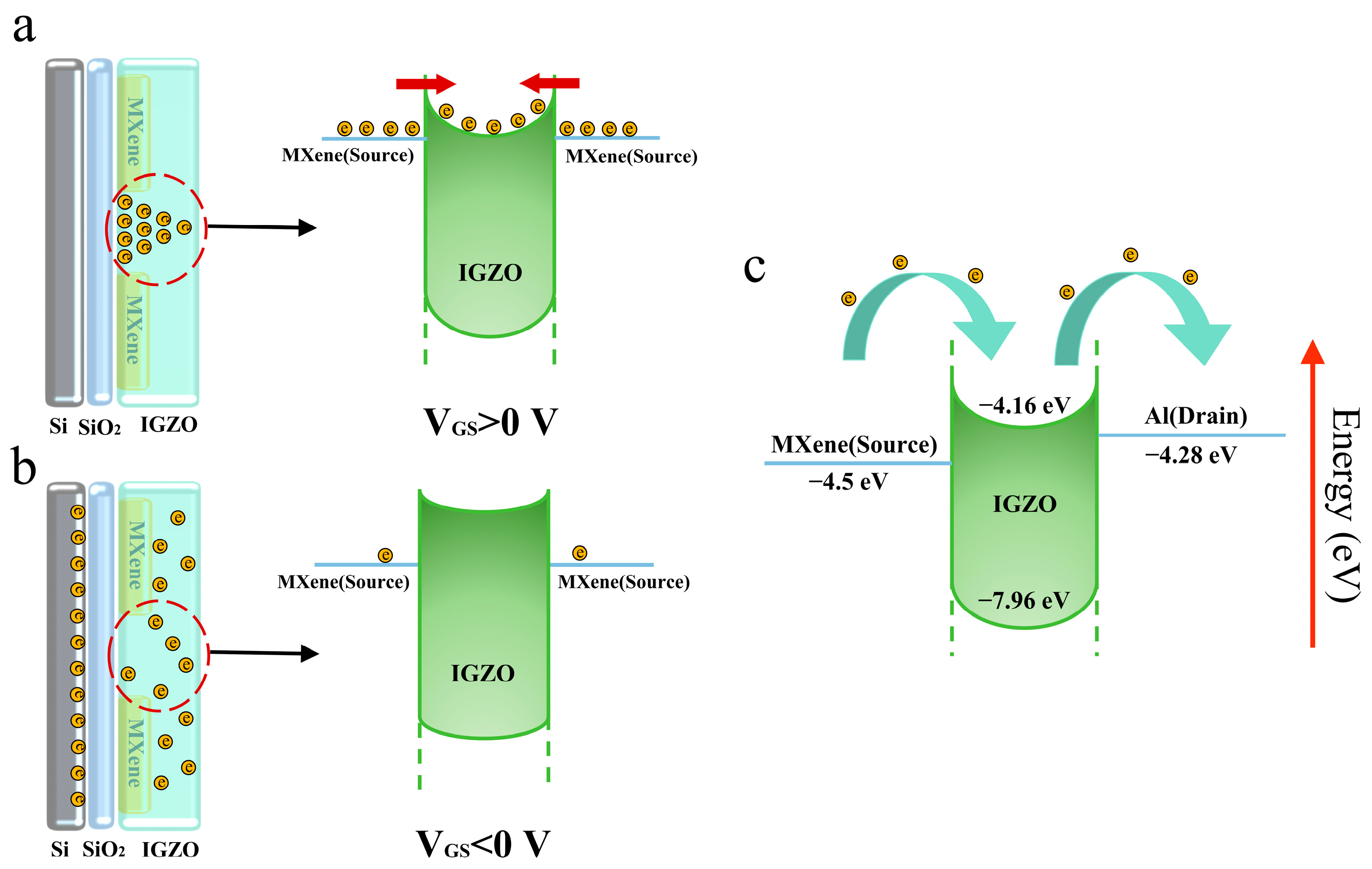
Figure 4 illustrates the working mechanism of the VC-IGZO-TFT. As depicted in
Figure 4b, when a negative gate voltage is applied, the electrons in IGZO are repelled from the interface between the MXene source electrode and IGZO channel layer, leading to an increase in the Schottky barrier (SB). Consequently, the electrons cannot cross the barrier, and the device remains in the off state. Conversely, as shown in
Figure 4a, when a positive gate voltage is applied, the electrons are accumulated in the pore of the source electrode at the interface between the SiO
2 and IGZO. The accumulation induces band bending in the IGZO layer, which effectively lowers the Schottky barrier height and facilitates electron tunneling from the source electrode into the channel layer. Consequently, the device transitions to the on state, allowing the current to flow from the source to the drain.
Figure 4c presents the corresponding energy-level diagram of the VC-IGZO-TFT device, demonstrating that under a positive
VGS, the electron injection from the MXene source electrode into the IGZO channel layer is enhanced, further enabling efficient charge transport.
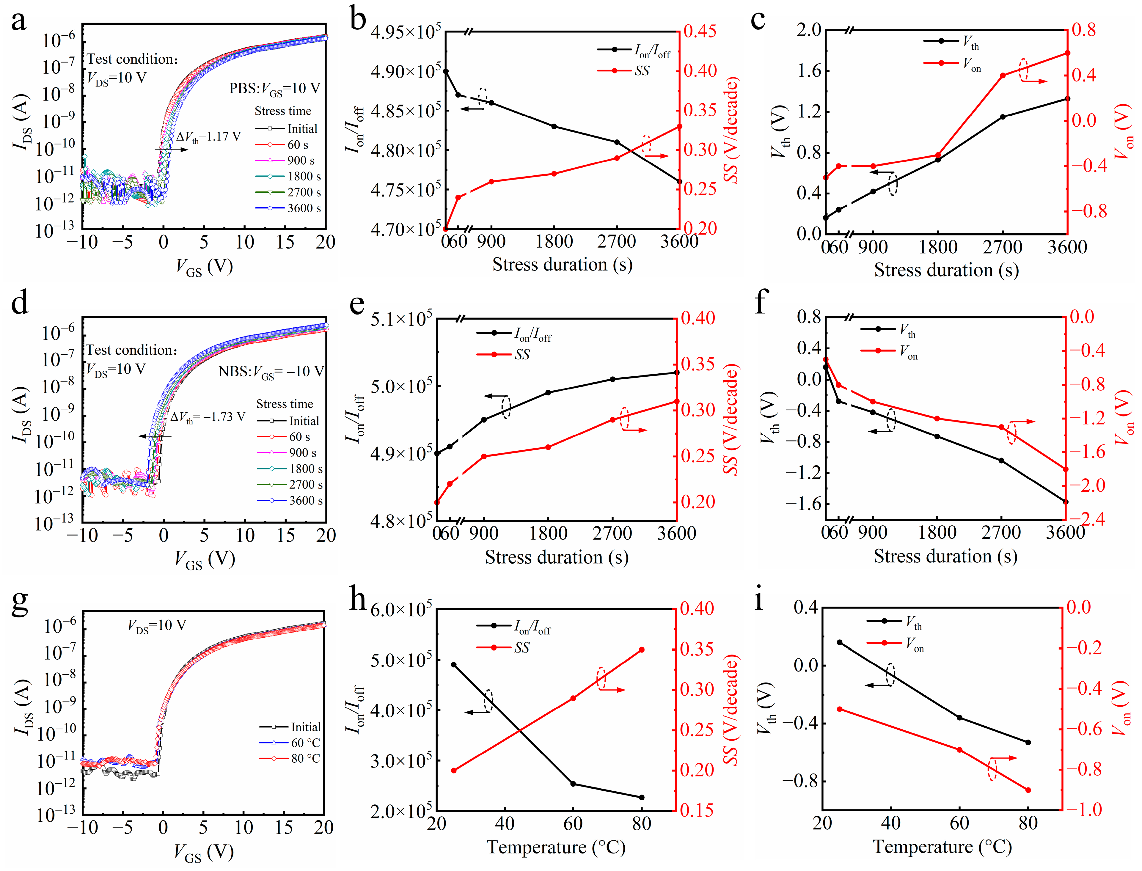
Bias stress stability testing is an essential technique for evaluating the long-term performance stability of transistors. In this study, the VC-IGZO-TFT based on a 3.0 mg/mL MXene source electrode was subjected to both positive gate bias stress (PBS) and negative gate bias stress (NBS) to evaluate its electrical stability.
Figure 5a–f presents the transfer characteristics and corresponding variations in the performance parameters under PBS at V
GS = +10 V for stress durations ranging from 0 to 3600 s. Following PBS exposure, the SS increased from 0.20 V/decade to 0.33 V/decade, while the I
on/I
off exhibited a slight decrease, from 4.90 × 10
5 to 4.76 × 10
5. Additionally, the V
on and V
th shifted by 1.1 V and 1.17 V, respectively. Under the NBS conditions (V
GS = −10 V) for the same duration, the SS increased from 0.20 V/decade to 0.31 V/decade, while I
on/I
off remained relatively stable, varying only slightly from 4.90 × 10
5 to 5.02 × 10
5. The corresponding shifts in V
th and V
on were −1.73 V and −1.3 V, respectively. The minimal variations observed in the electrical properties of VC-IGZO-TFTs after 3600 s of PBS and NBS indicate excellent bias stress stability. In addition to electrical stress, the impact of thermal stress on the device performance was examined at different temperatures, as shown in
Figure 5g–i. When the temperature increased from room temperature to 60 °C and 80 °C, the SS exhibited a moderate increase from 0.20 V/decade to 0.29 V/decade and 0.35 V/decade, respectively. Concurrently, I
on/I
off decreased from 4.90 × 10
5 to 2.45 × 10
5 and 2.27 × 10
5, primarily due to a rise in the off-state leakage current. Moreover, V
th shifted negatively from 0.16 V to −0.36 V and −0.53 V, while V
on decreased to −0.7 V and −0.9 V at 60 °C and 80 °C, respectively. The degradation in the performance at elevated temperatures is attributed to thermally activated carriers and increased defect-state excitation in the IGZO layer, which contribute to threshold voltage shifts and increased leakage.
The VC-IGZO-TFTs are characterized by a current flow that is oriented vertically through the semiconductor material, distinguishing them from planar transistors where the current flows horizontally. To fabricate flexible VC-IGZO-TFTs, the rigid silicon substrate and silicon dioxide (SiO
2) gate insulator were replaced with transparent polyimide (PI) and a high dielectric constant hafnium oxide (HfO
2) gate insulator, respectively. To assess the mechanical robustness, the devices were subjected to repeated bending at various angles.
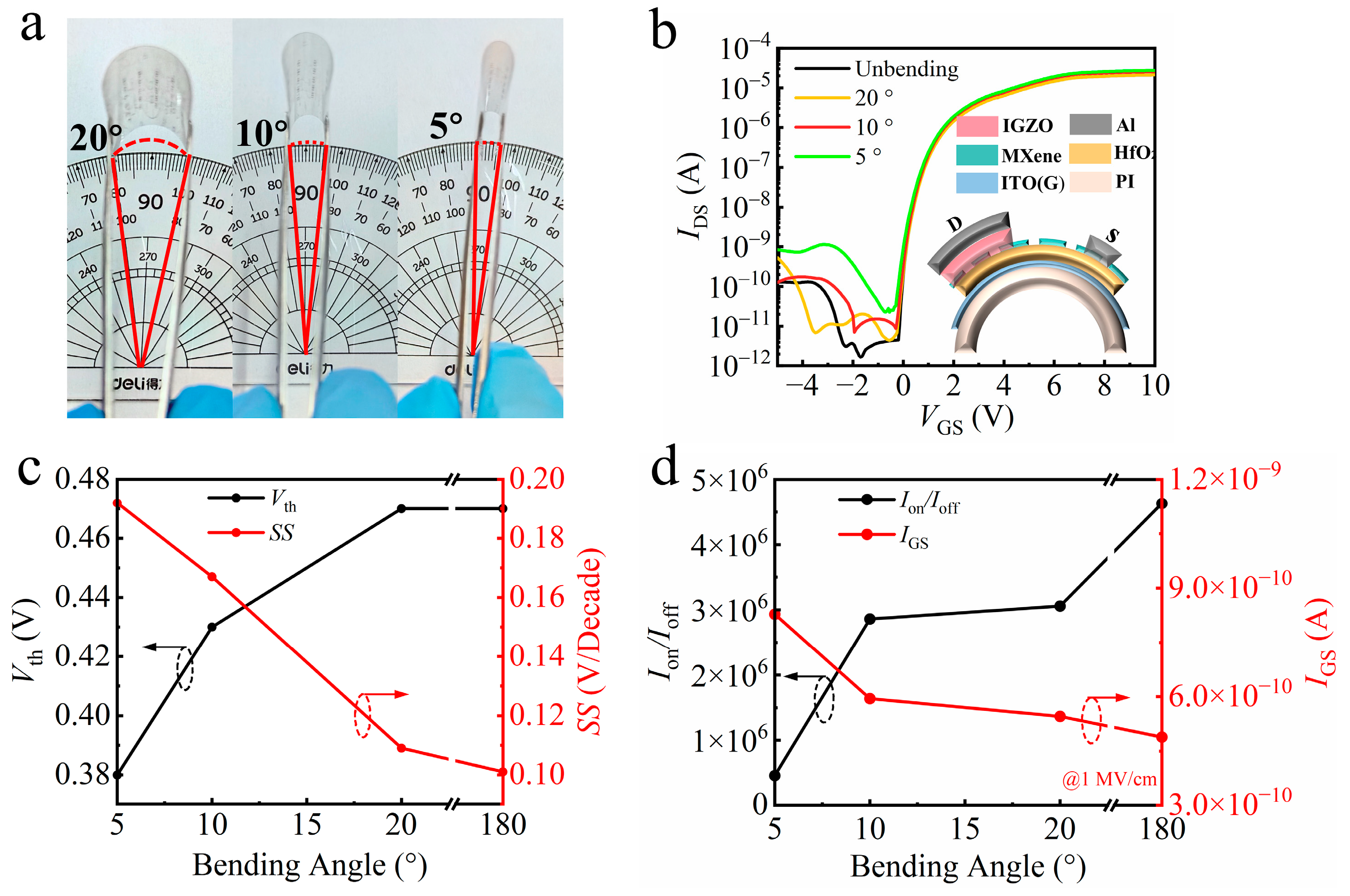
Figure 6a schematically illustrates the bending angles discussed in this work, where smaller angles correspond to more severe bending.
Figure 6b presents the transfer characteristics after 100 bending cycles at different angles, with the inset showing a cross-sectional view of the VC-IGZO-TFT fabricated on a PI substrate. The results demonstrate that the devices maintain relatively stable transfer characteristics after 100 bending cycles at 10°and 20°, while a noticeable increase in the off-state current was observed after bending at 5°. The changes in the key electrical properties of VC-IGZO-TFTs subjected to 100 bending cycles at different curvature levels are depicted in
Figure 6c,d. Compared with an unbent device, the V
th slightly decreases from 0.47 V to 0.38 V, and the SS value increased from an initial 0.101 V/dec to 0.192 V/dec, indicating minimal sensitivity to mechanical deformation. The unbent device achieves an I
on/I
off of 4.63 × 10
6, which decreases to 3.06 × 10
6, 2.86 × 10
6, and 4.59 × 10
5 after bending at 20°, 10°, and 5°, respectively. This degradation primarily results from a significant increase in the off-state current. Moreover, the gate leakage current (I
GS), measured at V
GS = 6 V (corresponding to an electric field of 1 MV/cm), increased from 4.89 × 10
−10 A, 5.46 × 10
−10 A, 5.95 × 10
−10 A to 8.28 × 10
−10 A, indicating deteriorated gate insulation properties due to bending-induced defects, which enhanced the gate leakage current. The minimal change in the key electrical properties of VC-IGZO-TFTs demonstrates excellent mechanical stability, which can be attributed to the vertical structure that avoids in-plane cracks in the channel layer and is consistent with findings from previous studies on flexible vertical channel TFTs [
26].
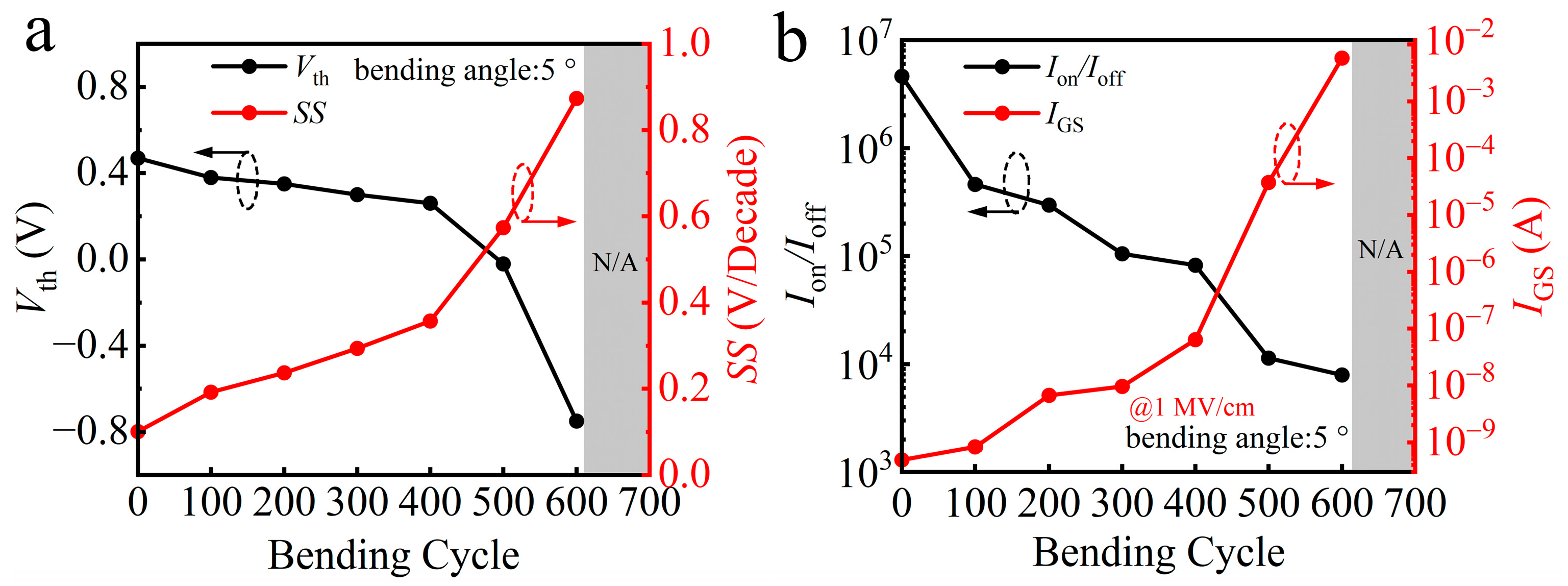
To further assess the impact of mechanical strain on flexible devices, the key electrical performance parameters of the flexible VC-IGZO-TFTs were examined under varying numbers of bending cycles at a fixed bending angle of 5°.
Figure 7a illustrates the evolution of
Vth and SS as functions of the bending cycle count. The device exhibits moderate degradation for up to 400 cycles, followed by a rapid deterioration beyond this point. Specifically, V
th shifts gradually from 0.47 V to 0.26 V as the number of cycles increases from 0 to 400. However, after 400 cycles, V
th experiences a pronounced negative shift, reaching −0.75 V at 600 cycles. Correspondingly, the SS gradually increases from 0.101 V/decade to 0.357 V/decade, followed by an abrupt rise to 0.873 V/decade, indicating the onset of severe electrical instability.
Figure 7b presents the variations in the I
on/I
off ratio and I
GS at 5° under the same bending conditions. The I
on/I
off ratio decreases significantly from 4.63 × 10
6 to 8.24 × 10
4 after 400 cycles and further drops to 7.9 × 10
3 after 600 cycles. Meanwhile, I
GS exhibits a gradual increase to 6.41 × 10
−8 A for up to 400 cycles, followed by a sharp rise to 5.79 × 10
−3 A at 600 cycles, suggesting the severe degradation of the gate insulating layer. These observations indicate that the flexible TFTs retain relatively stable electrical characteristics for up to 400 bending cycles at a bending angle of 5°. Beyond this threshold, accumulated mechanical strain induces defect generation in both the gate dielectric and the active channel layer, leading to a substantial leakage current and performance deterioration. Therefore, the results confirm that the devices exhibit excellent mechanical durability under repeated strain conditions for up to 400 cycles, maintaining acceptable electrical functionality.


 ,
, 


