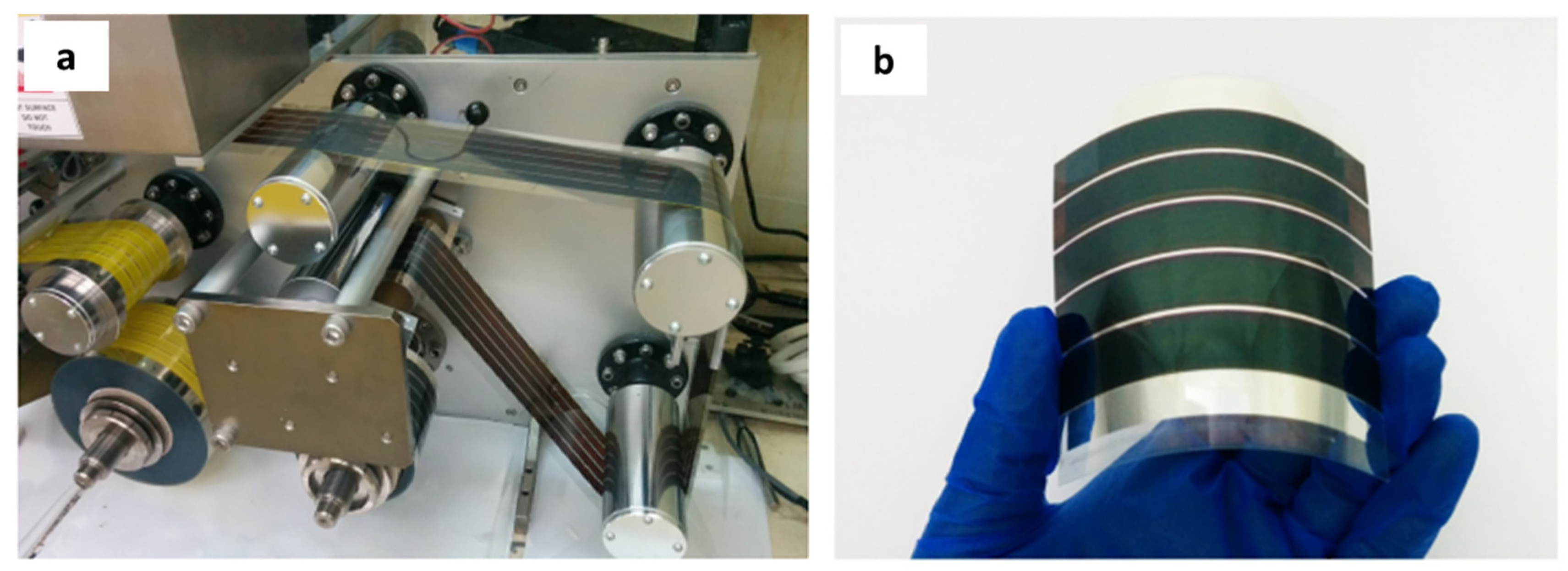
1. Introduction
With a record power conversion efficiency (PCE) of 26.1%, perovskite solar cells (PSCs) have shown the most impressive technological development among emerging photovoltaic (PV) technologies, reaching an efficiency comparable to that of mature crystalline Si solar panels in only a decade [
1]. Although Si-based technologies dominate the PV market, PSCs are highly appealing due to their exceptional performance; low cost; ease of processing; and capabilities such as different transparencies, colour tuning, shape-flexibility, lightweight panels, and enhanced capacity to efficiently harvest diffuse sunlight [
2]. These attributes give PSCs a strong potential to disrupt the PV field. Furthermore, one of the key features of PSCs is their compatibility with flexible substrates, enabling high-throughput roll-to-roll (R2R) manufacturing, which could attract major industry players [
3]. R2R processing not only allows for faster production compared to traditional silicon-based devices but enables the creation of modules in novel shapes.
Despite the tremendous evolution in efficiency, the commercialisation of PSCs faces several challenges, primarily related to long-term stability, lead toxicity, and upscaling to large-area devices. Addressing the latter issue requires the development of scalable coating techniques. Several processes, including spin-coating, blade coating, slot-die coating, spray-coating, and vacuum deposition, among others, have been explored for manufacturing large-area devices in an effort to upscale PSCs—
Figure 1 [
4,
5,
6,
7,
8,
9,
10]. While spin-coating is widely used at the laboratory scale, it is not suitable for preparing large-area devices due to high material waste, inability to control film thickness and homogeneity over large areas, and incompatibility with high-throughput R2R processing. Indeed, maintaining high efficiencies during the transition from the laboratory to industrial scale is one of the biggest challenges in this research field [
11,
12,
13,
14,
15,
16]. Slot-die coating is an easily scalable deposition technique that offers a unique combination of low material waste, precise control over film thickness, compatibility with online patterning, and compatibility with R2R processing [
17]. This review provides an overview of the most recent developments in the upscaling of PSCs using slot-die coating as the primary coating process and discusses the theoretical fundamentals and operational limits of the slot-die coating process.
2. Slot-Die Coating Fundamentals
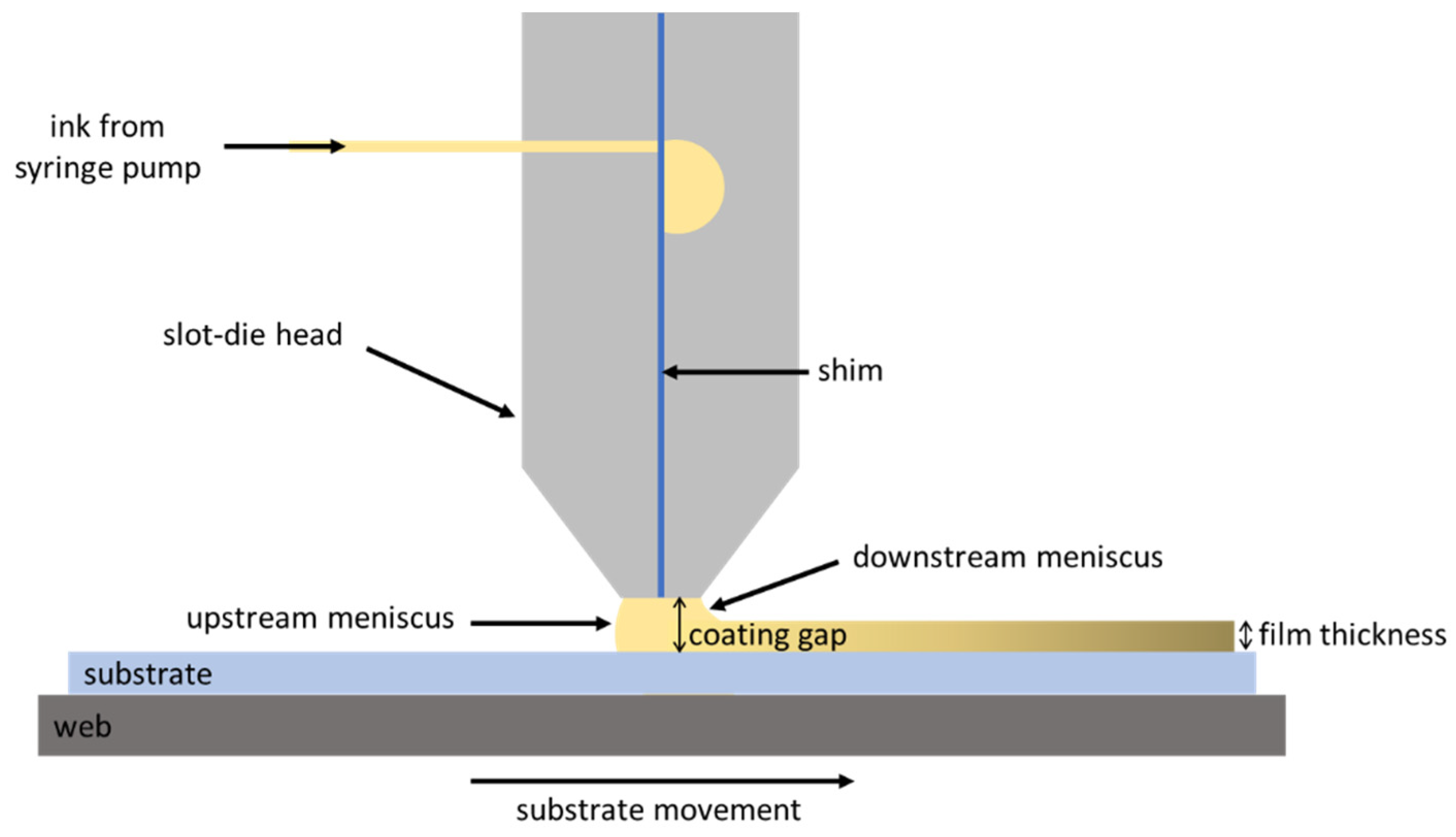
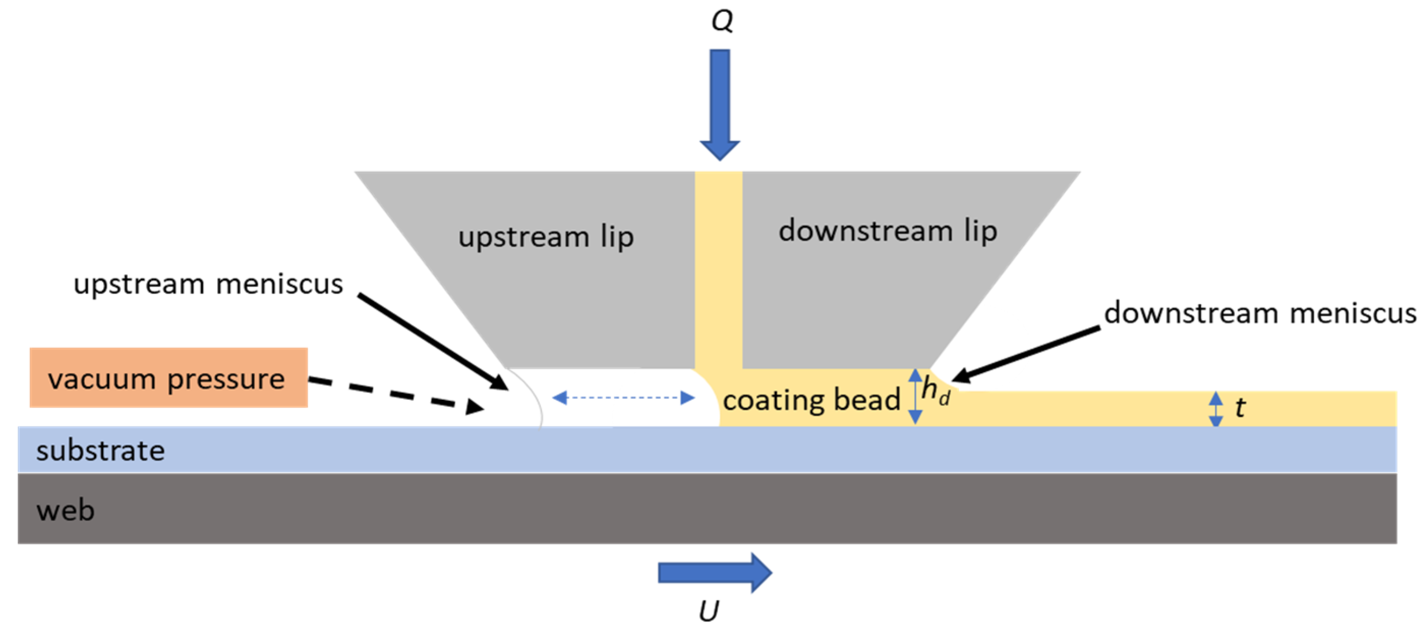
The slot-die coating is well suited not only for depositing the perovskite ink but also for the other inner layers of the device stack, including the hole transport layer (HTL) and the electron transport layer (ETL). In a conventional slot-die coating process, the coating head is positioned near the substrate, and then, the ink is pumped to the coating head using a syringe pump. The ink is then dispensed through a tiny slit along the length of the coating head (
Figure 2). The upstream meniscus displaces gas at the moving contact line, while the downstream meniscus creates the deposited wet film. The ink forms a bridge between the coating head and the substrate, resulting in the coating bead and the so-called meniscus. In some applications, a vacuum is applied at the upstream meniscus to stabilise the coating bead, assist in displacing gas, and improve substrate wetting [
18]. As a pre-metered coating technique, slot-die coating allows the precise adjustment of the substrate’s movement speed and the ink flow rate, determining the thickness of the dry film that is deposited. With minor adjustments to the ink flow rate and substrate speed, it is possible to coat films ranging from very thin (tens of nm) to much thicker (tens of µm) with extremely fine control over the dry film thickness [
19,
20,
21,
22]. Slot-die coating can also be integrated into R2R systems, offering high material usage, minimal waste, and excellent uniformity over large areas. These characteristics make slot-die coating the ideal method for high-precision coatings.
The coating process is significantly influenced by the type of ink being used. Nevertheless, according to Equation (1), the wet film thickness,
t, can be directly controlled by the flow rate,
Q, of the ink pumped to the slot-die head, as well as the web speed,
U, and its width,
w [
23]:
In manufacturing, the production rate is directly proportional to the speed at which the substrate can be coated. At low speeds, uniform coatings are easily achieved; however, for industrial purposes, such speeds are not economically viable. Higher speeds are required to meet manufacturing demands, which imposes the optimisation of operating parameters to achieve uniform and defect-free coatings.
3. Slot-Die Coating Operating Limits
The primary concern in the slot-die coating process is determining the operating limits to decide the proper range of parameters, such as the coating speed, the ink flow rate, the vacuum pressure, the coating gap, the ink viscosity, and the surface tension. This is an extremely complex issue, and several relevant concepts have been defined to characterise the deposition, namely the coating window, low-flow limit, and thinnest film thickness [
24]. The mechanisms underlying these limits have been extensively studied, yet their full understanding is still hampered by the diversity of materials with different intrinsic characteristics and the complexity of the competing forces acting on the coating bead, such as capillary, viscous, applied vacuum, inertial, gravitational, and elastic forces [
25,
26].
Knowing the operating limits in the slot-die coating process is very useful for determining the proper range of the operating parameters. The coating window is the range of operating conditions that yield a good quality coating. The coating layer should be free of defects if the operating conditions are within the coating window and the coating bead remains stable. Defects will arise when operating outside the coating window. Vacuum pressure can be applied to the upstream meniscus to increase the stability of the coated bead.
Understanding the coating window of a coating process can help determine whether a specific technique can coat a given substrate at a set production rate. Sartor [
23] originally proposed, and then Creel [
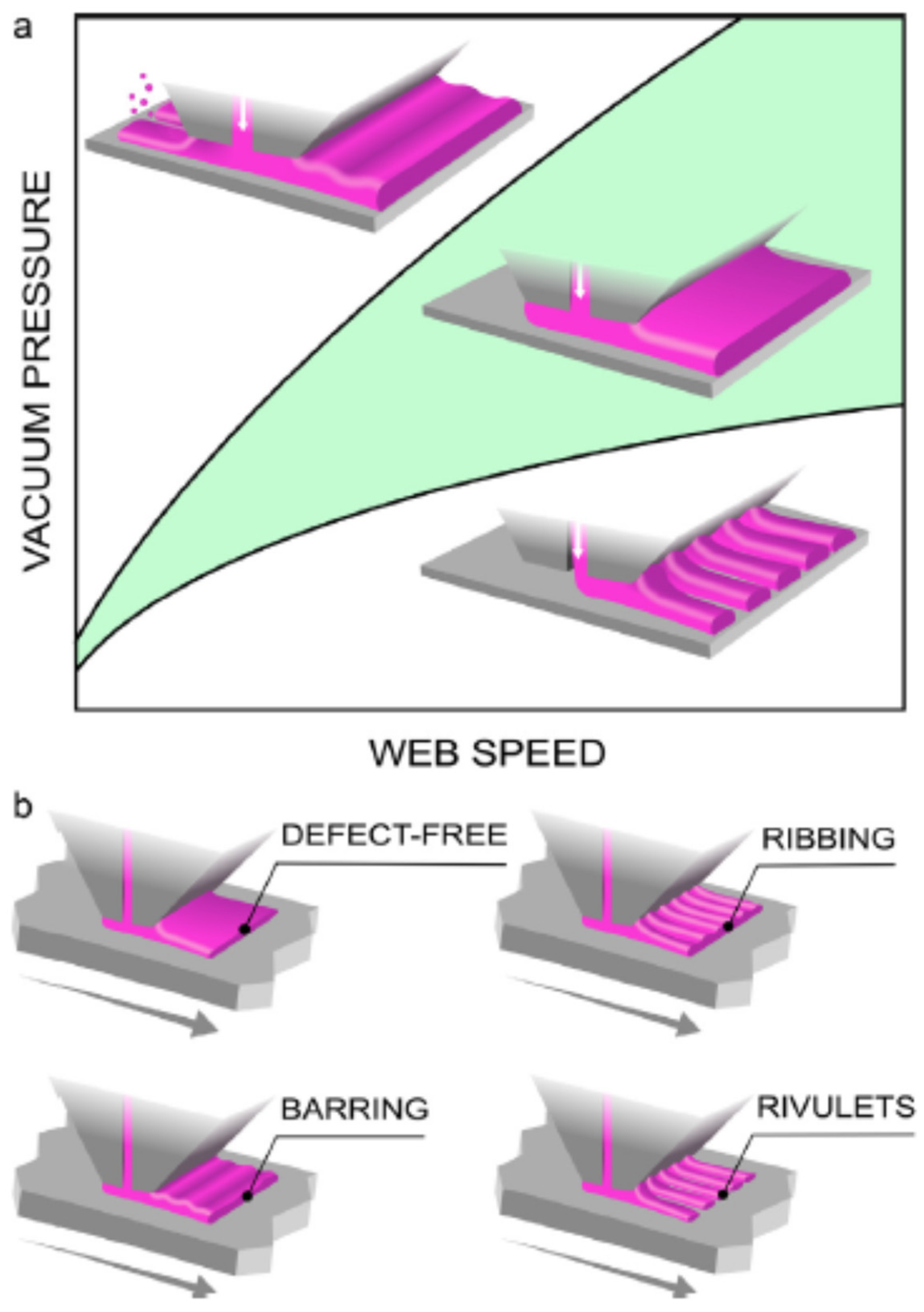
27] reproduced, that defect-free coatings can be obtained within a certain coating window for a given upstream vacuum pressure and coating speed range, as shown in green in
Figure 3a. This coating window depends on the ink, target wet film thickness, and slot-die coating gap. Outside the coating window, the film may not be continuous, or its thickness may vary. The modelled position of the upstream meniscus predicts the high and low vacuum pressure limits, often referred to as vacuum operability limits. These limits are defined as the conditions under which the upstream meniscus precisely rests at the uppermost corner of the upstream lip during continuous operation. As a result, while some common faults can be linked to operating outside these limits, they cannot be used to anticipate specific instabilities or defects (
Figure 3b) [
27]. Higher vacuum pressures (above the coating window) can draw the upstream meniscus past the upstream lip corner, potentially causing ribbing and rivulet coating defects, as well as upstream meniscus swelling and weeping. Conversely, very low vacuum pressures (below the coating window) can cause the upstream meniscus to retreat and invade the feed slot at high speeds, forming rivulets.
Ruschak [
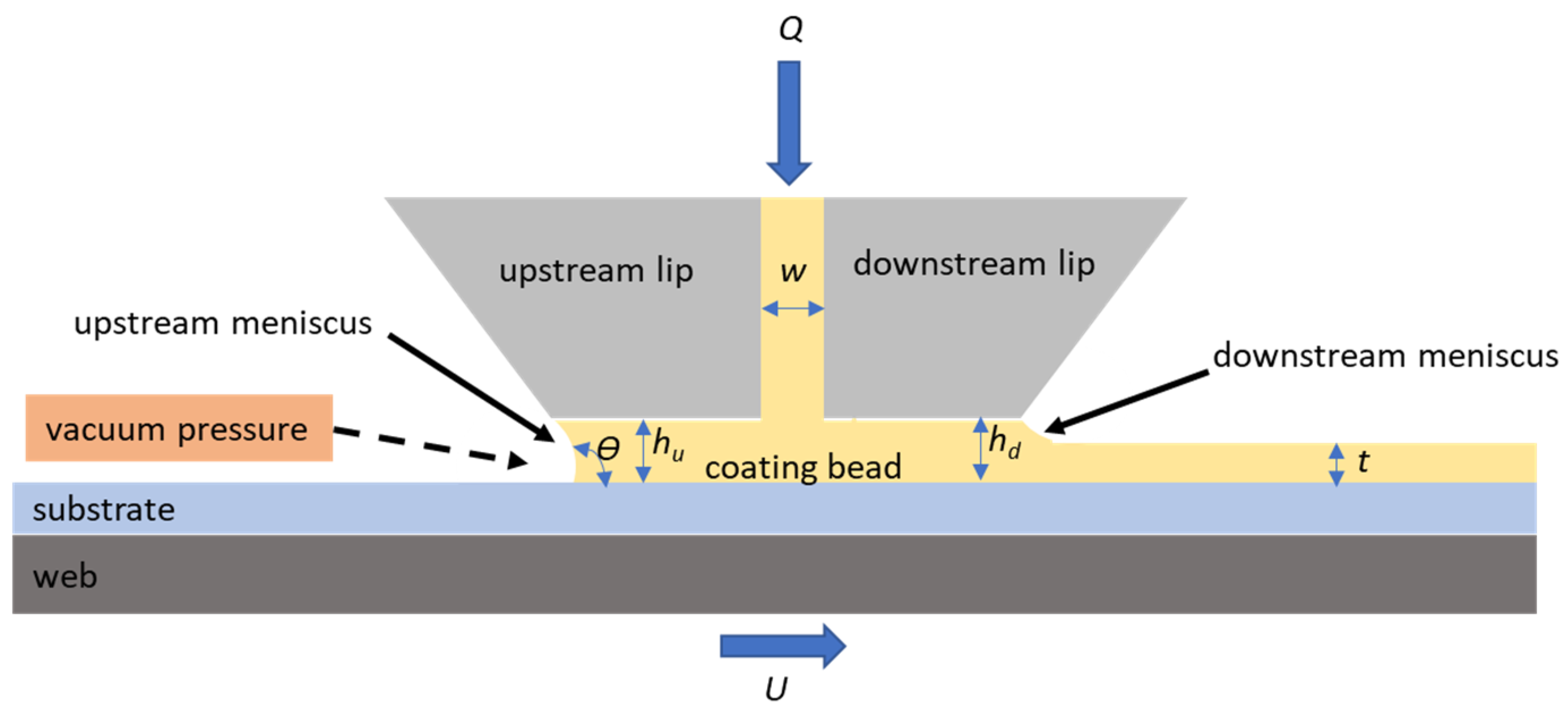
28] published the first theoretical analysis of the slot-die coating operating limits. The author investigated the stability of the coating bead during the application of vacuum pressure (
Figure 4). Analytical ranges for the wet thickness and vacuum pressure needed to create a stable coating bead were provided in this work. According to Ruschak, the capillary pressure in the coating bead mostly determines the operating limits in this case, as viscous effects are minimal. This operating limit model is known as the capillary model.
Since the capillary model is based on an extension of the Landau–Levich boundary conditions [
29], the capillary pressure, Δ
P, can be described using the following dimensionless equations:
where
Ca is the capillary number;
µ is the ink viscosity;
U is the substrate moving speed;
σd is the surface tension on the downstream meniscus;
t is wet film thickness. The capillary model only applies to small capillary and Reynolds numbers, because the Landau–Levich boundary condition assumes that both the flow rate and coating speed are approaching zero [
28,
29].
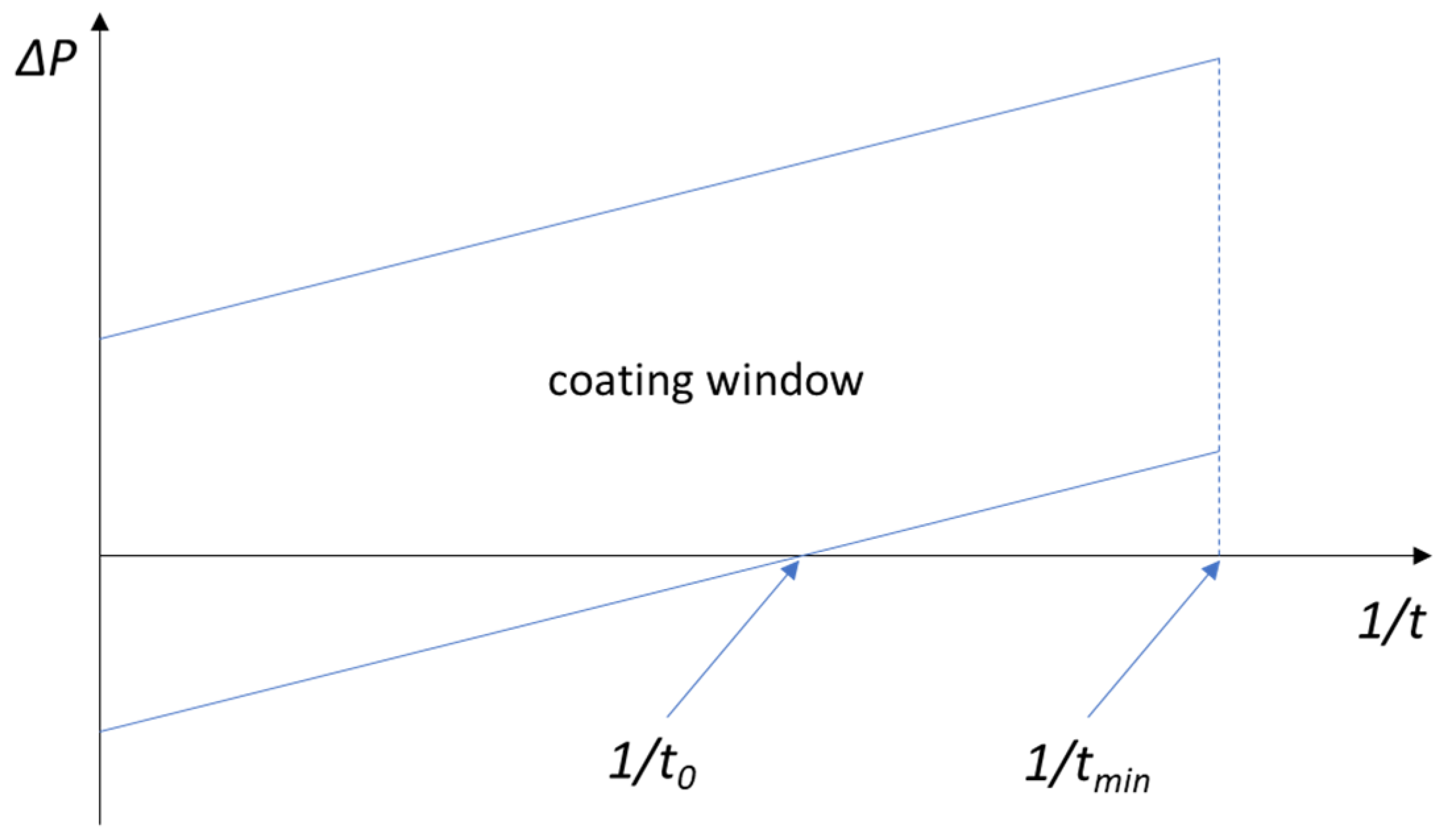
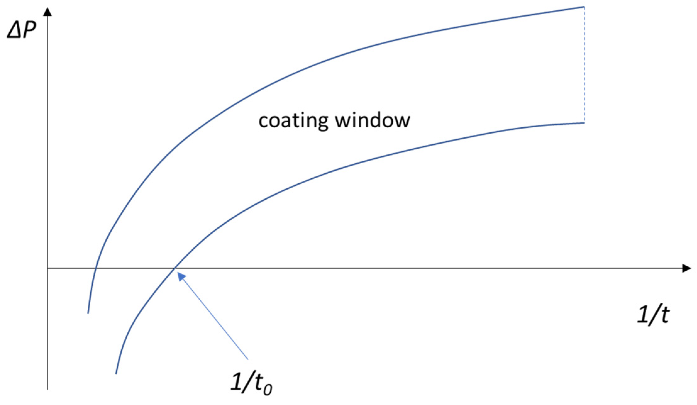
Figure 5 shows the coating window for the capillary model [
30]. The boundaries of the coating window reflect the maximum and minimum limits of the vacuum pressure restrictions. Equation (4) represents the lowest wet thickness,
tmin, for a given capillary number (
Ca) and downstream coating gap (
hd) for a slot-die coating process. This boundary is usually referred to as the low-flow limit.
The thinnest film thickness,
t0, corresponding to the thickness of the film when Δ
P is zero, can be obtained from the capillary model of the operating limit conditions as another significant result—Equation (5):
Subsequently, Higgins and Scriven [
30] examined the operating limits without considering the capillary effects, focusing solely on the viscous pressure on the coating bead. This model is known as the viscous model. In that case, as shown in
Figure 6, the upstream meniscus is free to move. Instabilities in the coating bead, such as variations in cross-web thickness and air bubbles, result from increasing the coating speed or decreasing the vacuum pressure. On the other hand, dripping defects occur when the upstream meniscus moves out of the die lip due to a decrease in coating speed or an increase in vacuum pressure.
In this case, there is no low-flow limit, because the Landau–Levich boundary condition is not valid due to the viscous model´s disregard for capillary effects. According to Equation (6), the
t0 of a viscous coating bead is equal to half of the coating gap downstream. Therefore, the capillary number has no bearing on the
t0; it only depends on the downstream coating gap. The coating window in this model is plotted in
Figure 7.
The operating limits become more complex when the capillary and viscous effects in the coating bead cannot be disregarded. In such cases, the capillary and viscous pressures in the coating bead determine the operating limits within the so-called viscocapillary model [
30]. The Landau–Levich boundary condition remains applicable for this model; therefore, the low-flow limit remains the same as shown in Equation (4), but the
t0 will be more complex—Equation (7).
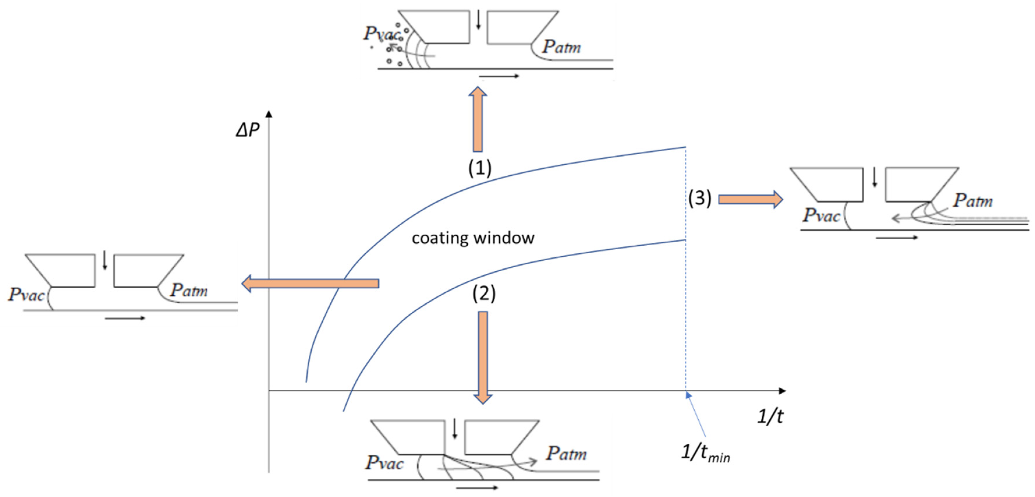
Figure 8 illustrates the coating window for the viscocapillary model and shows that the coating window is constrained by three failure modes [
31]:
- (1)
High-vacuum limit: Occurs when the liquid is drawn into the vacuum chamber due to the high vacuum applied at the upstream surface for coated layers with thicknesses t > tmin (at a fixed coating gap and coating speed), affecting pre-metering.
- (2)
Low-vacuum limit: Arises from an unbalance in the viscous forces on the upstream part of the coating bead, caused by the applied vacuum pressure and the capillary forces in the upstream and downstream meniscus, creating a pressure gradient and resulting in rivulets defects.
- (3)
Low-flow limit: Happens at a specific coating speed when the downstream meniscus curves excessively, preventing it from bridging the gap clearance (hd) due to an excessive low-flow coating rate per unit of width. This instability in the coating bead leads to the formation of rivulets and chains of droplets.
As mentioned earlier, the shape of the coating window changes with the varying capillary numbers, as the operating limits in both the capillary and viscocapillary models depend on the capillary numbers. Moreover, the viscocapillary model applies primarily to small capillary numbers, typically associated with low-speed coating and/or low-viscosity films (see Equation (3)). However, speed coating limitations may not meet the economic requirements of certain products, particularly those involving liquids with high viscosity.
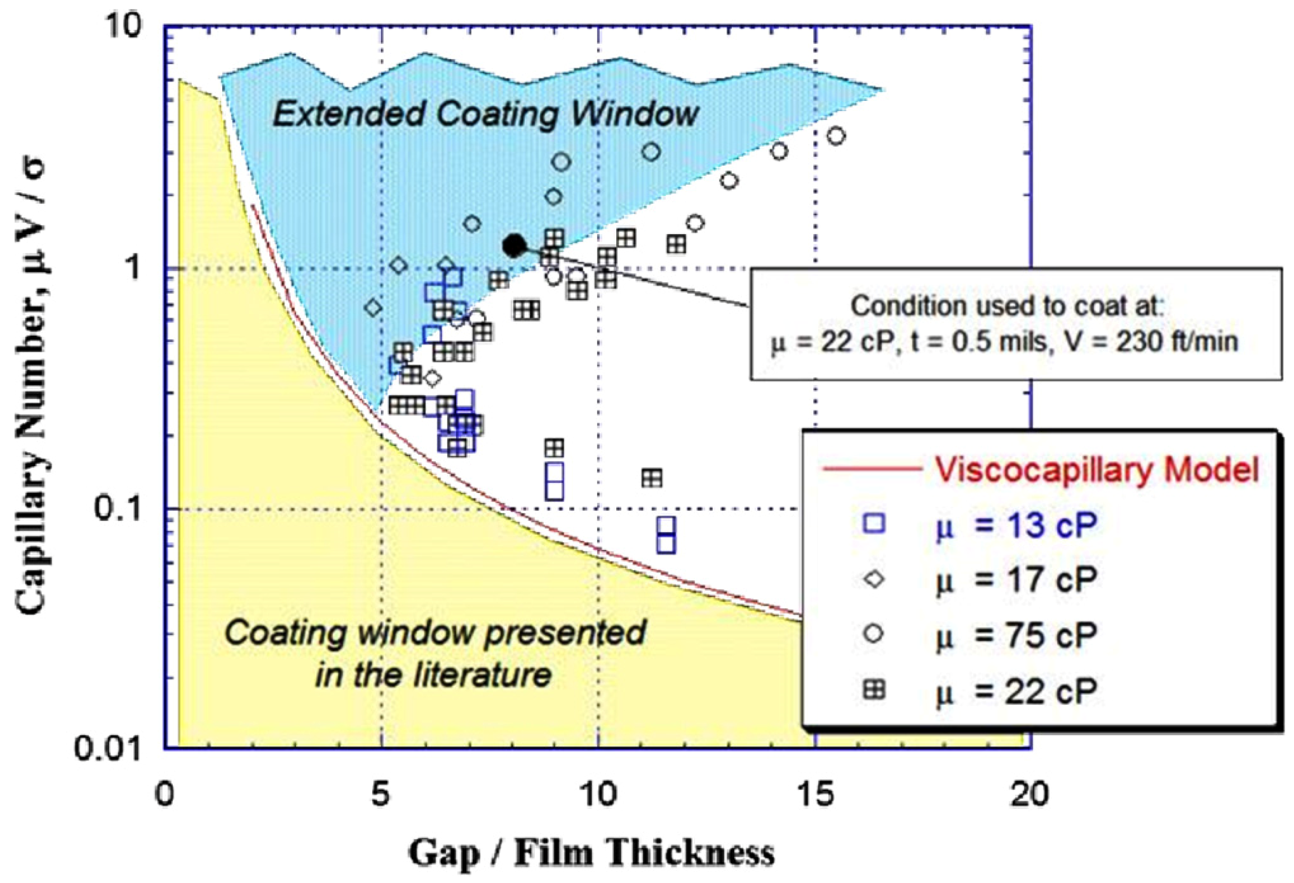
The low-flow limit at high capillary numbers and Reynolds numbers was further investigated by Carvalho and Kheshgi [
32], who demonstrated that the coating window for the process is significantly larger than reported for low capillary numbers. They showed how the inertia of the ink can delay the breakup into rivulets by pushing the downstream meniscus out of the coating bead at sufficiently high coating speeds. This resulted in an expanded coating window (
Figure 9), indicating a wider range for uniform coatings than previously reported and broadening the potential applications of slot-die coating processes.
Dynamic wetting failure is another issue that arises in slot-die coating processes [
24]. Dynamic wetting occurs in the slot-die coating when the coating ink displaces air, creating a dynamic contact line between the upstream meniscus and the moving substrate. The term “wetting speed” typically refers to the speed of the substrate. The dynamic contact line becomes unstable and breaks into a sawtooth shape when the wetting speed exceeds a critical value (
Ucrit) [
34]. This phenomenon is referred to as dynamic wetting failure and often indicates the presence of air entrainment defects. The critical wetting speed (
Ucrit) can be expressed by the following equation:
where
Cacrit is the critical capillary number that corresponds to the maximum wetting speed,
µ is the ink viscosity,
Ucrit is the maximum wetting speed, and σ is the surface tension.
Since dynamic wetting is a crucial aspect of industrial coating processes, it is essential to fully comprehend its precise mechanism. Theories concerning molecular kinetics and hydrodynamics at the macro and micro scales can explain the dynamic wetting phenomenon. Vandre and co-workers [
35] investigated the influence of meniscus confinement on dynamic wetting behaviour. Their theoretical studies revealed that the inability to displace air from the dynamic wetting line results in wetting failure due to unbalanced viscous and capillary pressures. At high-speed coating (greater than
Ca), viscous effects distort the air/liquid meniscus, causing the dynamic contact line to move towards the substrate. When the critical speed (
Ucrit) is reached, air bubbles form in the liquid, destabilising the dynamic contact line (
Figure 10). Equation (9) provides an approximate expression for the critical capillary number based on their experiments:
where
K is a coefficient of the critical capillary number in the expression relating to the maximum wetting speed. Equation (10) defines the capillary length,
lcap, which indicates that this result is only valid for a coating gap smaller than the capillary length:
where
σ is the ink density, and
g is the acceleration of gravity. When the coating gap is excessively large, the confinement effect becomes negligible, suggesting that meniscus confinement is not necessary when using high coating speeds in the slot-die coating process.
In fact, beyond the limits already mentioned, there are other operating limits, such as die configuration [
24], positive shims [
22], and meniscus guides [
36], in addition to the coating window, low-flow limit (
tmin), thinnest film thickness (
t0), and the dynamic wetting failure previously described. For instance, studies have shown that installing positive shims and meniscus guides in the space between the upstream and downstream lips of the slot-die head can enhance slot-die coating parameters and coating uniformity when preparing PSCs, especially in R2R processes. Understanding the physical mechanisms and coating flows associated with various failure modes in the slot-die coating process facilitates improved process design, significantly reducing process development and production time when introducing new products to the market.
4. Advancements in Slot-Die Coating for PSCs Upscaling
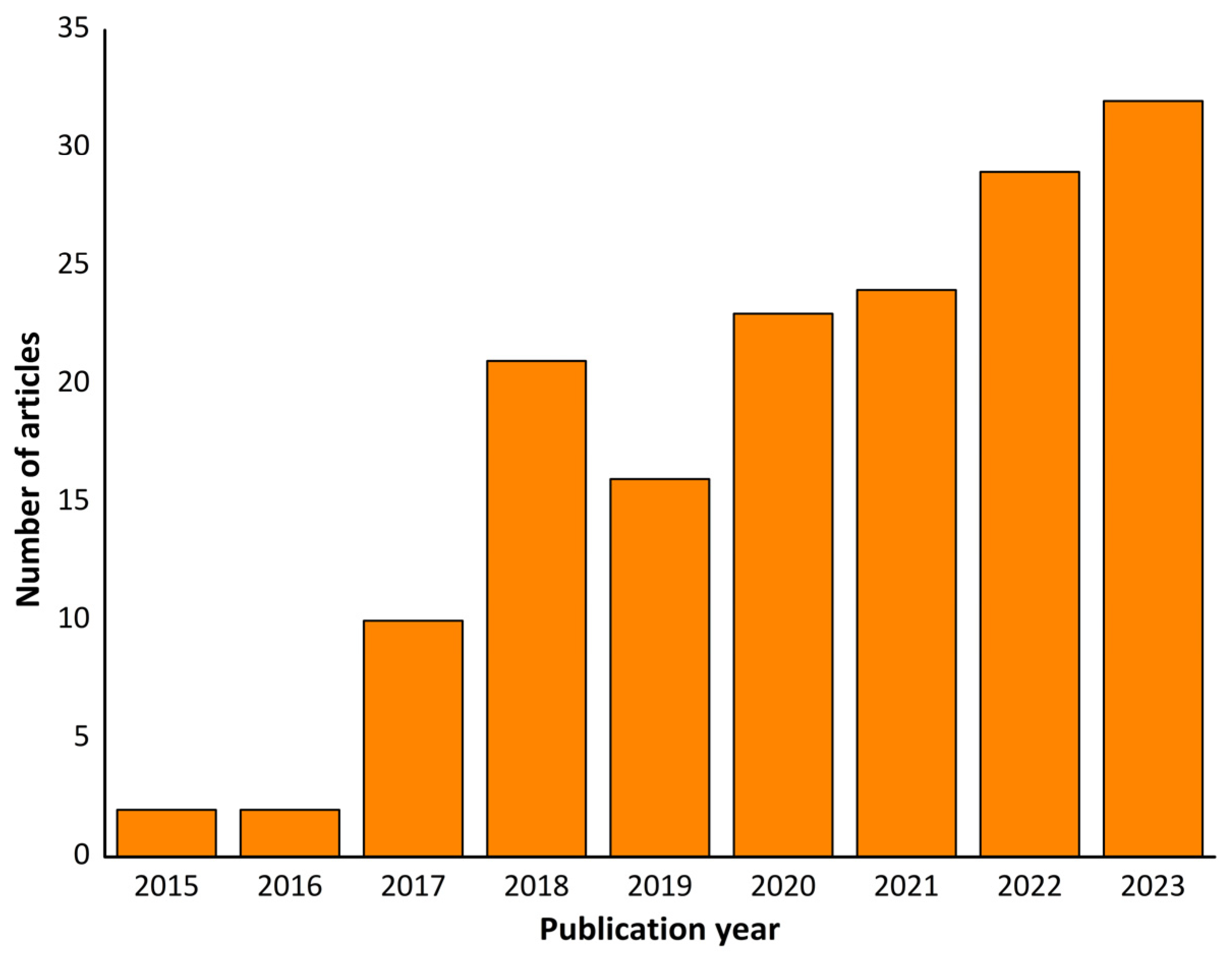
Recent years have seen a growing number of reports on PSCs utilising slot-die technology (
Figure 11). Most studies focus solely on slot-die deposition of the perovskite layer, recognising its critical impact on PSC performance. While slot-die coating can achieve uniform wet films on large-area substrates, challenges arise during drying, often leading to pinholes and cracks post-annealing [
17]. Therefore, optimising the drying conditions is crucial for enhancing the perovskite film quality and crystallisation, thereby improving the efficiency of large-area devices produced via slot-die coating.
Vak and his co-workers employed slot-die coating for the first time to prepare PSCs [
37]. They prepared the perovskite layer in planar devices with the configuration ITO/ZnO/MAPbI
3/P3HT/Ag using slot-die coating, achieving PCEs exceeding 11%. A sequential deposition process was employed to fabricate the perovskite layer: PbI
2 films were first slot-die-coated and then converted to MAPbI
3 via a dipping process. To control the drying process and ensure film uniformity across the perovskite surface, a flow of nitrogen—“gas blowing”—was used. Following this pioneering work, Hwang and his group reported fully slot-die-coated PSCs, in which only the back contact was evaporated [
38]. Using the PSC configuration ITO/ZnO/perovskite/P3HT/Ag, a champion device efficiency of 11.96% was achieved. Again, a two-step deposition procedure was employed for the perovskite layer deposition: first, the PbI
2 layer was slot-die-coated and dried using N
2 gas quenching, followed by slot-die coating of the MAI solution onto the PbI
2 layer.
These early studies showed the versatility and potential of slot-die coating for scaling up PSCs. Since then, considerable work has been undertaken to use slot-die coating to prepare large-area PSCs, focusing primarily on depositing a specific active layer.
Figure 12 shows the evolution of power conversion efficiency over time for perovskite solar modules deposited using the slot-die technique, and
Table 1 presents some representative results from these efforts.
4.1. Perovskite Layer
Since the perovskite layer is crucial to the performance of PSC devices, achieving a defect-free film with large grains, a pure crystal phase, and adequate film coverage is imperative for enhanced photovoltaic stability and performance. Two deposition strategies have been developed to enhance the quality of the slot-die-coated perovskite films. These include (1) one-step perovskite deposition, suitable for larger industrial processes due to its simplicity and shorter coating time, and (2) two-step perovskite deposition, allowing the separation of the film formation, which can be advantageous for optimising the perovskite layer quality. For instance, Zimmermann and co-workers demonstrated the use of the two-step perovskite deposition in large areas using slot-die coating for both forming the lead iodide layer and converting it into the perovskite structure [
50]. Control over perovskite crystallisation was achieved with this method, resulting in a dense and uniform perovskite layer. The lead-based precursor layer was intentionally porous to facilitate infiltration of the organic precursor layer in the second step, ensuring complete conversion to the perovskite phase. Modules with a 12 cm
2 aperture area were fabricated, and a PCE of 15.2% was obtained. Similarly, the two-step procedure was used to deposit triple-cation perovskite films on the SnO
2 electron transport layer for PSC module fabrication [
55]. First, CsI and PbI
2 were deposited, followed by vacuum quenching, and then, the organic precursor solution containing MaCl as an additive was applied. A PCE of 18.1% was achieved for modules with 37.6 cm
2 of active area.
In addition to perovskite layer deposition, other strategies have been employed to control perovskite film formation. These strategies include (i) drying methods, which enhance perovskite film nucleation rates, leading to high surface coverage and defect-free films; (ii) precursor selection, where a suitable choice of perovskite precursors yields improved surface coverage and morphology; (iii) solvent selection, an effective tool for controlling the perovskite film morphology; (iv) additives and surface modification, which affects crystal growth and morphology to improve stability and efficiency; and (v) slot-die coating parameters, which, adequately optimised, can further enhance the perovskite layer quality [
65]. Combining one or more of these strategies can significantly enhance the PSC device performance and the overall quality of the perovskite layer. An overview of the most important works within these different strategies will be presented next.
4.1.1. Drying Methods
The primary goal of the antisolvent approach frequently used in the spin-coating technique is to guarantee a prompt perovskite nucleation trigger. However, this technique contributes to excessive solvent waste during manufacturing processes and is not suitable for large-area depositions. Therefore, it has been shown that heating the perovskite layer and quenching it externally using an air knife produces very uniform perovskite films, mimicking the self-quenching step that happened in the spin-coating procedure—
Figure 13a,b [
66]. The temperature gradient created by the substrate heating suppresses the vertical growth of perovskite crystals, promoting horizontal perovskite crystal growth. This results in a smoother film with higher surface coverage. Additionally, by withdrawing more energy from the top of the film, the air knife increases the temperature gradient and further suppresses vertical crystal growth. To accelerate nucleation and solvent evaporation in perovskite film formation, Kim and co-workers combined blowing and heating to prepare perovskite films with high quality from a dimethylformamide (DMF) solvent system. This led to the formation of void-free perovskite films and enhanced surface coverage—
Figure 13c [
67].
In another study, Cai and co-workers developed a gas-pumping method to quickly evaporate the DMF solvent used in the slot-die-coated perovskite solution [
39]. This drying method effectively prevents pinhole formation and eliminates structural defects in perovskite films over large areas. Even after 140 days under outdoor conditions, 5 × 5 cm
2 modules that achieved 10.6% PCE showed no significant efficiency loss. A 45 × 65 cm
2 module and a demonstration power plant consisting of 32 perovskite panels were assembled using this method.
NIR (near-infrared irradiation) is another promising approach for quick and effective heating. High-quality crystalline perovskite films with high efficiencies were formed by using this method instead of the traditional heating method for post-annealing perovskite films [
68]. The main advantage of NIR technology is its ability to reach high temperatures quickly, unlike the several minutes required for traditional heating. Huang and co-workers prepared perovskite layers in large-area modules of 4 × 4 cm
2, consisting of six cells connected in a series (3.78 cm
2 of active area), using the NIR heating procedure [
46]. An increase in NIR absorption and wettability was observed when
n-butanol was added to the perovskite precursor solution, allowing for the formation of uniform perovskite films in less than 20 s. A PCE of 10.34% was reached for the device structure of FTO/NiO
x/perovskite/PCBM/PEI/Ag prepared in air conditions. Despite its modest efficiency, this method offers a fast-annealing process for perovskite formation, which can be useful for the mass production of PSCs.
High-pressure nitrogen extraction (HPNE) was the method that Du et al. employed to promote perovskite crystallisation [
5]. Large-grain perovskite films with high density are formed when the high nitrogen pressure used in HPNE significantly lowers the coating’s surface temperature and speeds up solvent extraction. Additionally, the PCE of the PSCs prepared with this strategy proved to be independent of almost all slot-die coating parameters (coating speed, liquid rate, and N
2 flow pressure), except for the concentration of the precursor solution. Thus, the high-quality perovskite films prepared within a wide processing window should be associated with the HPNE strategy, and the mechanism underlying this process was investigated—
Figure 14. At room temperature, HPNE causes the printed film to begin to crystallise into the yellow and α-phase after an initial amorphous phase. The transition to the black phase marks the end of the crystallisation process. The stabilised yellow phase is the most important intermediate for the fabrication of high-quality perovskite films over large areas. Furthermore, the perovskite surface was passivated with an ionic liquid ([M
4N]BF
4), which increased the PCE by reducing surface defects. The potential of this strategy for large-area PSCs was demonstrated by preparing PSC modules with an area of 40 × 40 mm
2. The best-performing module had an active area of 7.92 cm
2 (10.2 cm
2) and a PCE of 19.6% (18.6%).
To replicate the role of the antisolvent dripping used in spin-coater deposition, Bernard and co-workers developed a strategy utilising vacuum aspiration quenching in a one-step perovskite slot-die deposition [
51]. Vacuum aspiration is expected to result in a slower extraction rate compared to the antisolvent method, where solvent extraction is virtually instantaneous. Comparing the dense and homogeneous perovskite films obtained by the antisolvent method with those obtained by vacuum quenching, several pinholes are visible. However, combining vacuum aspiration with the addition of methylammonium chloride (MACl) to the perovskite precursor solution results in dense and pinhole-free films. The optimal molar ratio of MACl:FAI (0.3:1) for the perovskite cation precursors produced the best-performing devices. The scalability of this method was demonstrated by preparing a 12 cm
2 module with six sub-cells of 2 cm
2 using the slot-die-coated perovskite layer at the optimised MACl ratio and vacuum extraction process, reaching a promising PCE value of 13%.
Drying methods combined with temperature control significantly influence the crystallisation kinetics of the perovskite and the quality of the perovskite films formed, which directly impacts the performance of the PSC devices. This is particularly important for deposition on large-area devices, where uniformity is mandatory for high efficiency, and for deposition techniques where self-quenching methods are not used, such as slot-die deposition.
4.1.2. Precursor Selection
Device performance of PSCs is highly influenced by the morphology of the perovskite film; large crystals and uniform and pinhole-free morphology are often required for highly efficient PSCs. Improved perovskite film quality has been demonstrated for spin-coating techniques when alternative lead sources such as lead chloride (PbCl
2) and lead acetate (PbAc
2) replace the typical PbI
2 [
69,
70]. PbCl
2 has been reported to improve the crystal formation of the perovskite CH
3NH
3PbI
3−xCl
x [
71]. However, the presence and role of Cl in the perovskite layer formation are still under investigation, and no clear consensus has been reached. Zhang and co-workers studied the influence of several lead sources in the perovskite crystal formation [
72]. They used PbCl
2, PbI
2, and PbAc
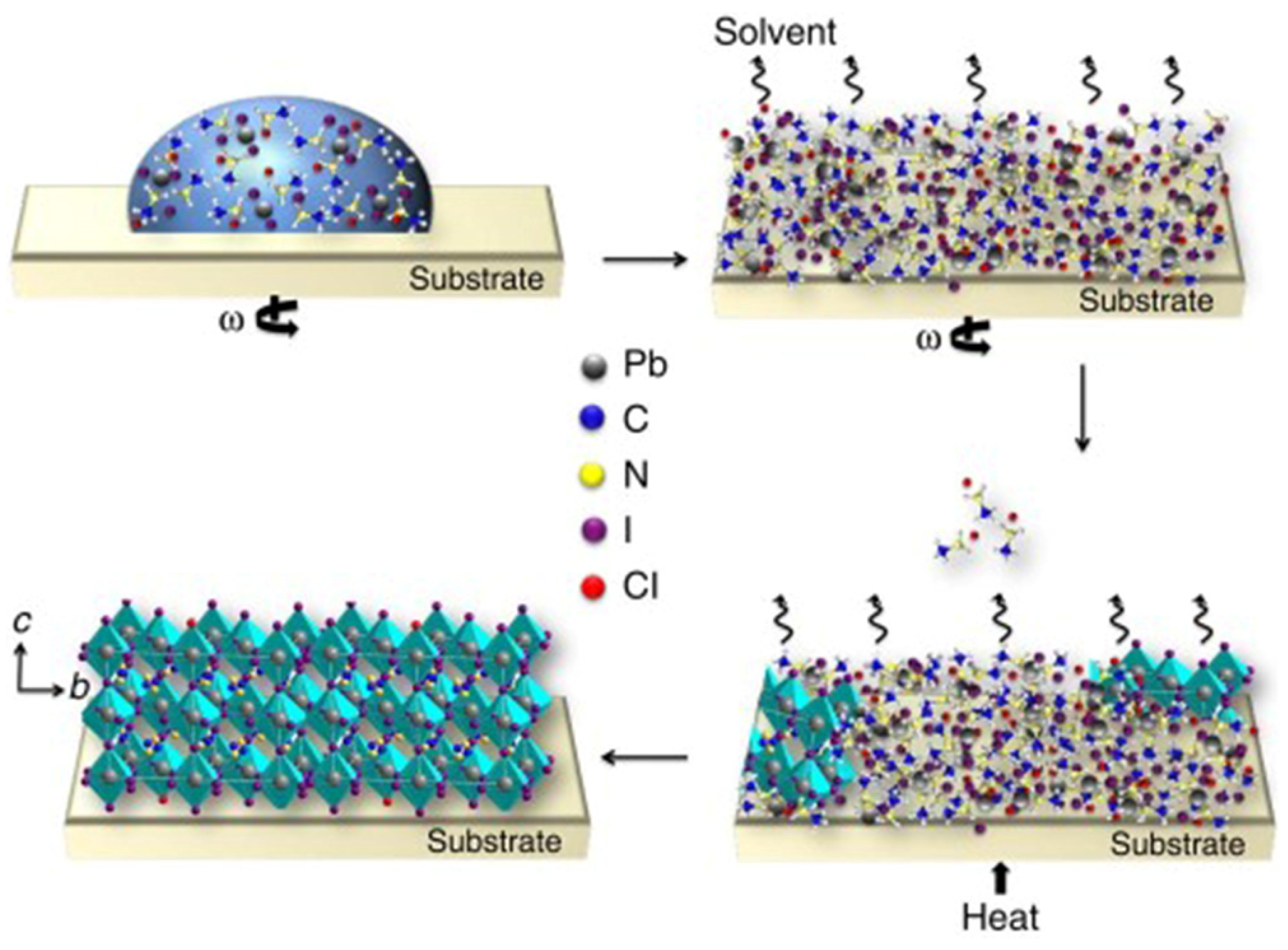
2 in conjugation with MAI in a three-molar excess. In all cases, no anion was detectable in the final perovskite film, but different film properties were found. They suggested that, during the first stage, solvent evaporation occurs, and the excess organic precursor remains entrapped in the wet film, retarding the crystallisation of perovskite. Then, full crystallisation of perovskite is achieved as the excess organic component is expelled from the film, with the time of this process being highly dependent on the by-product. If the by-product is not volatile, high sintering temperatures and long sintering times are needed to fully crystallise the perovskite film. An illustration of the proposed stages for the fabrication of CH
3NH
3PbI
3−xCl
x film is presented in
Figure 15. It was found that using PbAc
2 as a lead source results in the rapid crystallisation of perovskite film due to the high volatility of the by-product MAAc. This resulted in enhanced smoothness, surface coverage, and pinhole-free perovskite films. These properties of PbAc
2 favour scalable techniques such as slot-die coating, where self-quenching processing is absent, and the shorter annealing time will also impact manufacturing costs. However, the rapid crystallisation of PbAc
2-based perovskite films can result in small crystals, potentially increasing the defects and trap densities, which can reduce performances [
73]. To address this issue, mixed lead precursors, consisting of PbCl
2 and PbAc
2, have been shown to improve film morphology in spin-coated PSCs [
74].
Building on these findings, Lee et al. reported a highly reproducible method for the deposition of perovskite layers by slot-die coating under ambient conditions using PbAc
2 and PbCl
2 as the lead sources [
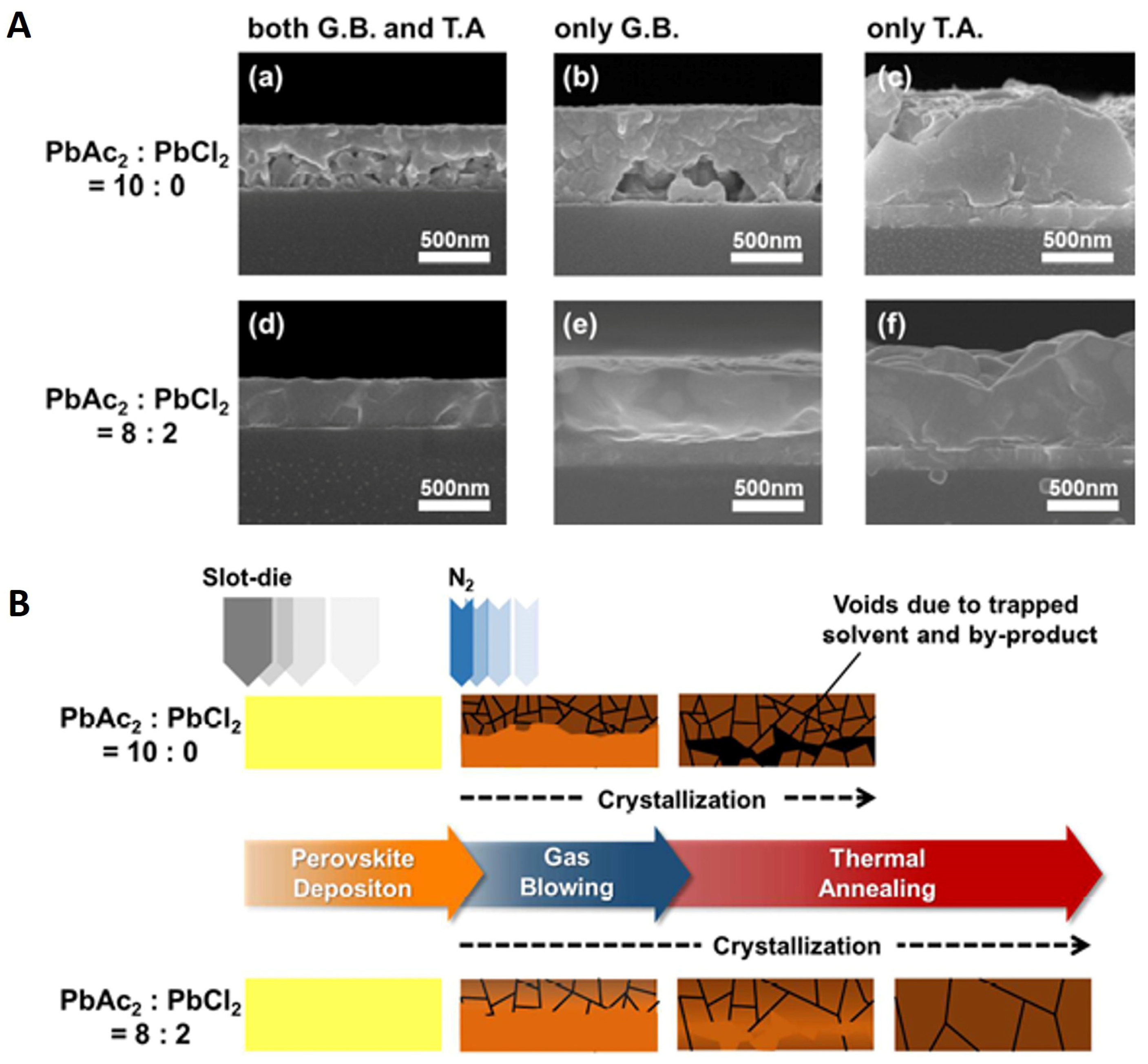
40]. A comprehensive investigation was carried out to examine the effects of various lead sources on the morphology of the perovskite layer, incorporating thermal annealing and gas-blowing techniques. It was demonstrated that using only the PbAc
2 lead precursor produced a nonuniform perovskite layer with large voids. In contrast, the perovskite produced with a mixed lead precursor of PbAc
2:PbCl
2 in an 8:2 ratio showed a very uniform morphology with well-grown grains over the whole thickness of the layer (
Figure 16A). These mixed lead precursors harness the benefits of both elements while mitigating their individual drawbacks. PbAc
2 facilitates fast crystallisation and a completely covered film morphology, while PbCl
2 enhances the grain size of the perovskite film. Moreover, it was shown that flat and uniform perovskite films from mixed lead precursor systems can be significantly improved by combining the thermal annealing and gas-blowing methods (
Figure 16B). The enhanced perovskite morphology achieved using mixed lead sources enabled the successful preparation of a 10 cm
2 PSC module by slot-die coating with a power conversion efficiency of 8.3%.
To produce PSC devices with performance matching those prepared by spin-coating, Giacomo and co-workers used the mixed lead precursors approach and demonstrated the scalability of the slot-die coating process they developed [
41]. Using a planar n-i-p structure (ITO/
c-TiO
2/CH
3NH
3PbI
3−xCl
x/spiro-OMeTAD/Au), slot-die coating was used to fabricate the perovskite and HTL layers. Compared to perovskite films produced from other lead sources, the perovskite precursor mixture of Pb(CH
3CO
2)·3H
2O, PbCl
2, and CH
3NH
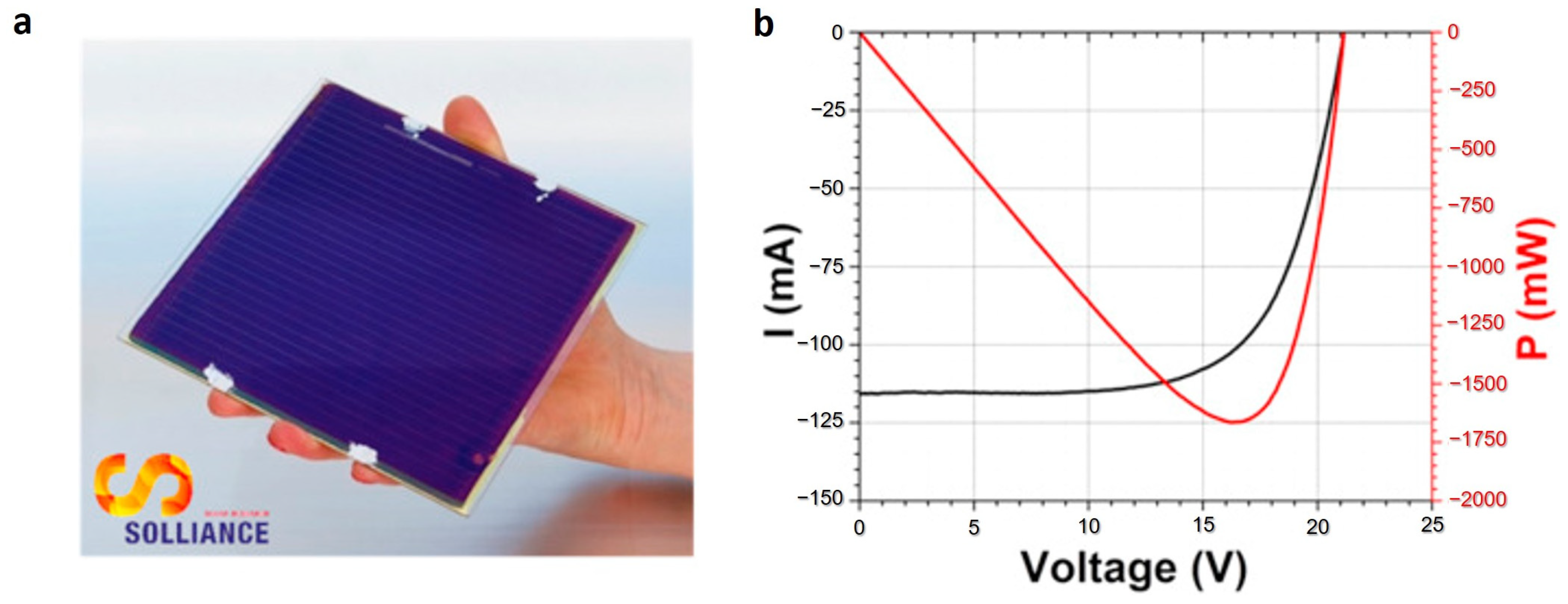
3I allowed for faster crystallisation and improved perovskite film morphology. The rapid crystallisation process combined with a single perovskite layer deposition step resulted in a remarkably uniform and pinhole-free perovskite layer. Using the developed slot-die coating process, large-area PSC modules with 168.75 cm
2 (12.5 cm × 13.5 cm) consisting of 25 series interconnect cells with a geometrical fill factor of 90% were fabricated. An active area PCE of 11.1% was recorded (
Figure 17).
Methylammonium (MA) is the organic cation most commonly used in perovskite formulations, but its insufficient thermal stability has led to its replacement by other cations. The formamidinium (FA) cation is used as a substitute for the MA cation due to its higher conductivity and narrow band gap [
75]. However, pure FA-based perovskites still face stability issues, especially at high humidity, as the α-cubic phase (black phase), which is responsible for the good3. properties, decomposes into the δ-tetragonal phase (yellow phase) [
76]. To address this, cesium (Cs) ions are being introduced to form mixed cation perovskites (FA
xCs
1−xPbI
3), which provide greater structural stability. Fievez and co-workers were the first to deposit FA-Cs-based perovskites on large-area substrates (10 × 10 cm
2) by slot-die coating [
77]. They used 16% Cs in the perovskite precursor formulation, because a higher Cs content can facilitate the formation of the α-cubic phase, while a lower content leads to mixtures of the α-phase and δ-phase. When this ink was used in conjugation with N
2 quenching and heating the substrate at 60 °C, a very uniform and compact perovskite film was formed.
The choice of perovskite precursors is undoubtedly a complex problem given the different cation and anion sources and possible mixtures. It is clear that, with a careful selection of perovskite precursors, faster perovskite crystallisation and better film quality can be achieved. When combined with an appropriate drying method, highly efficient PSCs and modules can be produced using slot-die coating.
4.1.3. Solvent Selection
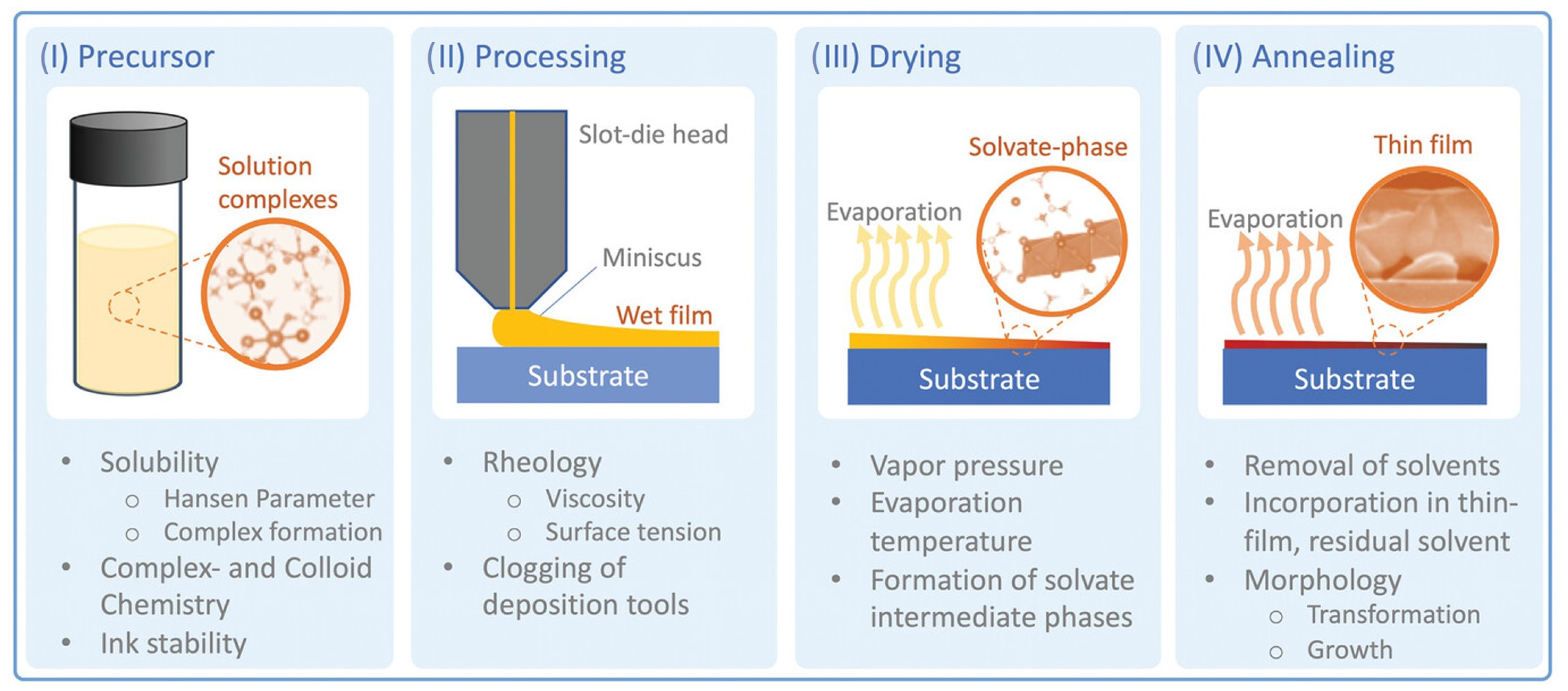
The solvent used in the perovskite precursor solution serves several functions that can impact the quality of the perovskite layer during its crystallisation steps (see
Figure 18). Firstly, the solvent must dissolve the perovskite precursors at a sufficiently high concentration to achieve the desired perovskite layer thickness in a single deposition. Secondly, the viscosity of the ink is crucial for ensuring uniform coating. Thirdly, the boiling point of the solvent plays a critical role in solvent evaporation during perovskite crystallisation. Finally, solvents can form adducts with perovskite intermediates that influence the growth and morphology of the perovskite film. For the slot-die coating process, the low viscosity and low boiling point of the precursor solution solvent are particularly important because of its limited drying capacity and the operating limits of this deposition technique. An appropriate choice of precursor solution solvent will boost the coating speed and reduce the drying time, essential for scaling manufacturing processes. DMF is the most commonly used solvent. To prevent the premature precipitation of PbI
2, a small amount of other solvents such as dimethylsulfoxide (DMSO) is typically added due to its high boiling point [
78].
Giacomo et al. demonstrated that perovskite crystallisation homogeneity can be controlled through customising the ink formulation [
42]. By incorporating cosolvents and additives into the perovskite ink precursor, perovskite nucleation occurs more uniformly, resulting in reduced pinhole density. When coupled with a rapid drying technique (quenching), this ink produced low-roughness perovskite films in spin-coated PSC devices. Scaling up this process using slot-die coating yielded no significant losses, enabling the deposition of the three main layers of a PSC module with a 144 cm
2 aperture area, achieving a PCE of 13.8%.
Subsequently, Li and co-workers effectively slot-die-coated MAPbI
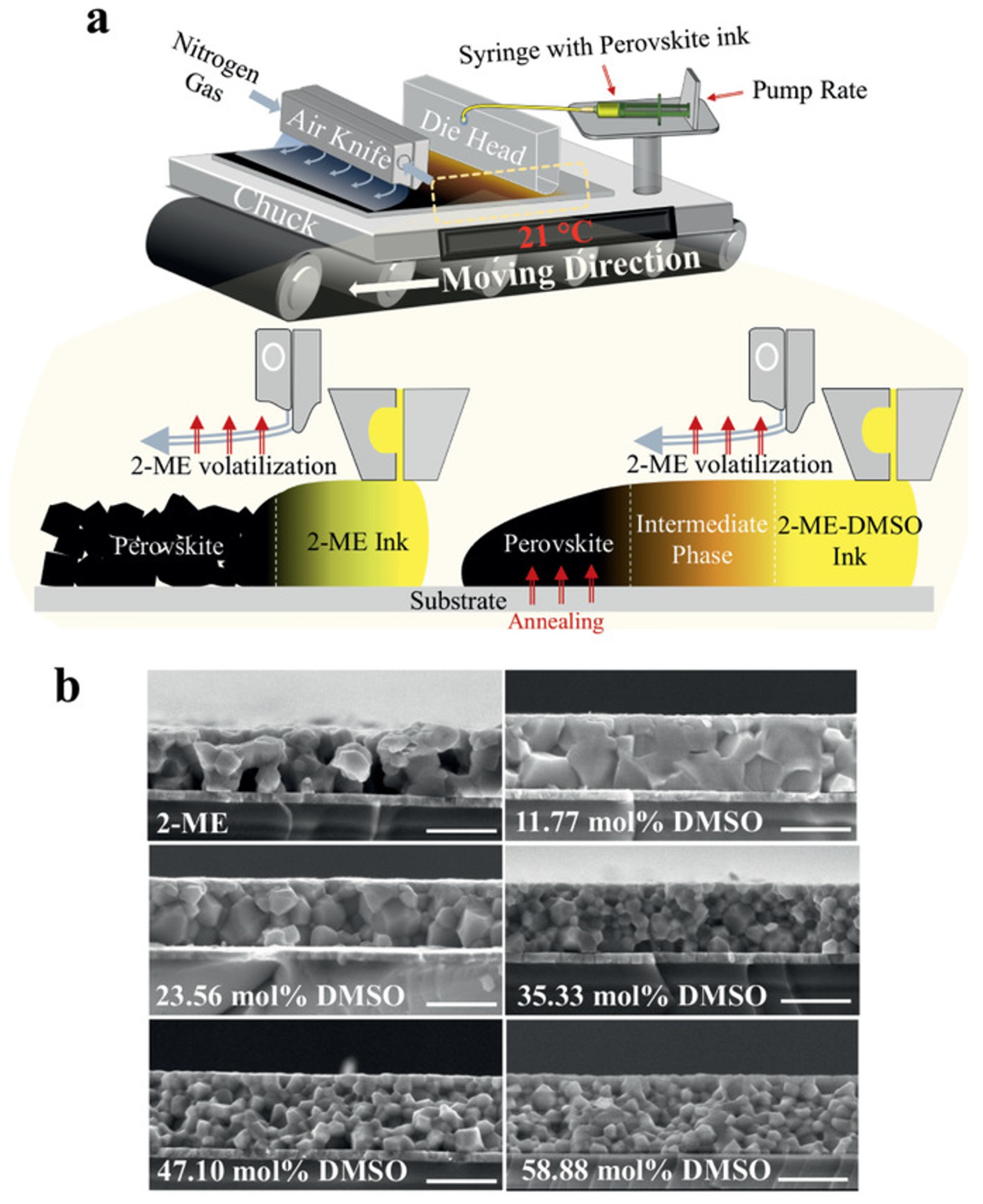
3 films using a highly soluble and low boiling point 2-methoxyethanol (2-ME) ink [
48]. They enhanced the quality of perovskite films by adding the strongly coordinating DMSO solvent to the perovskite precursor solution (
Figure 19a). Perovskite films prepared with pure 2-ME were found to be discontinuous and porous (
Figure 19b) due to rapid solvent evaporation during coating and air knife gas quenching, leading to quick and disordered crystallisation of the perovskite. The addition of small amounts of DMSO significantly altered the perovskite morphology, resulting in denser films with larger crystals and no pinholes (
Figure 19b). Using the optimised ink formulation, PSC modules with 2.5 × 2.5 cm
2 (2.2 cm
2 of active area) were slot-die-coated. The champion module achieved a PCE of 14.6% with negligible hysteresis.
On the other hand, Bu and co-workers investigated the nucleation kinetics and crystal growth of FA
0.83Cs
0.17PbI
3 perovskite film using DMF and
N-methylpyrrolidinone (NMP) as solvents [
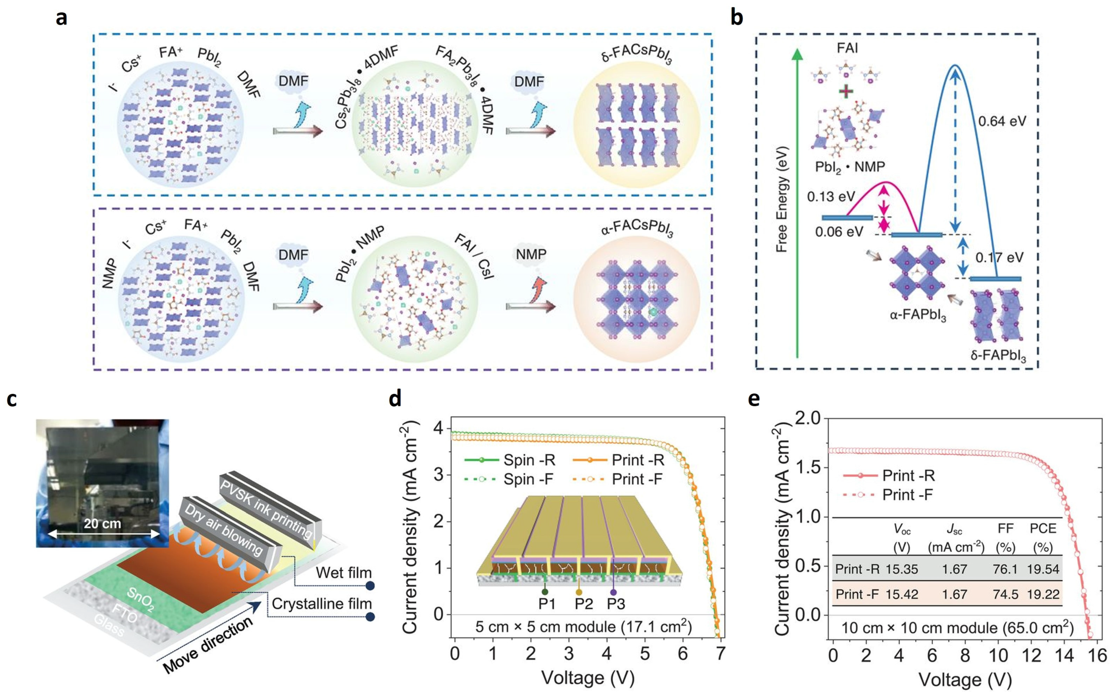
6]. They observed that using DMF alone resulted in a rough perovskite film with dendrites, large holes, and some densely packed large grains after complete drying. Despite efforts to enhance the solvent removal through spinning and the formation of intermediate solvent-coordinated complexes (Cs
2Pb
3I
8·4DMF and FA
2Pb
3I
8·4DMF), the nucleation rate remained low during drying. Consequently, the δ-FACsPbI
3 phase (porous) formed (
Figure 20a), and it was quickly annealed at 150 °C to become the α-FACsPbI
3 (dense). The addition of NMP to the perovskite precursor solution resulted in the formation of the strong adduct PbI
2·NMP (
Figure 20a), which dominated the nucleation. The homogeneous distribution of FAI/CsI species during film formation contributed to well-controlled film morphology, significantly reducing the formation energy of α-FACsPbI
3 (
Figure 20b). Defects and traps during the δ- to α-phase transition were suppressed due to direct conversion into the α-phase. The addition of an excess of PbCl
2 to the precursor solution formed the PbX
2·0.5NMP·0.5DMF adduct, suppressing FA
2Pb
3I
8·4DMF nuclei and resulting in a denser perovskite film. To enhance the photovoltaic performance and stability and eliminate hysteresis, KPF6, a potassium-based salt, was added to the perovskite precursor solution. Large-area modules were fabricated using the optimised perovskite precursor solution via a gas-assisted slot-die coating process (
Figure 20c). The performance of the spin-coated and slot-die-coated modules was comparable (
Figure 20d). A hysteresis-free module achieved a PCE of 19.54% over a masked area of 65 cm
2, using a 10 × 10 cm
2 slot-die-coated module with 14 sub-cells connected in a series (
Figure 20e).
Following this research, Yang and co-workers employed the same solvent system to formulate a perovskite precursor solution for depositing the perovskite layer in PSC devices using a two-step slot-die coating method [
53]. Initially, a FA
0.83Cs
0.17PbI
3 perovskite film was prepared to achieve a pure α-phase perovskite. Then, a second post-treatment with FAI was used to react with the unreacted PbI
2 and rectify any compositional defects. This approach resulted in a FA-rich perovskite film with larger grains, which increased the short-circuit current density. A 10 × 10 cm
2 slot-die-coated PSC module with an aperture area of 60.84 cm
2 was manufactured with a PCE of 17.56%. This work provided a straightforward approach to address the quality challenges of the FA-rich perovskite films prepared via scalable deposition techniques like slot-die coating.
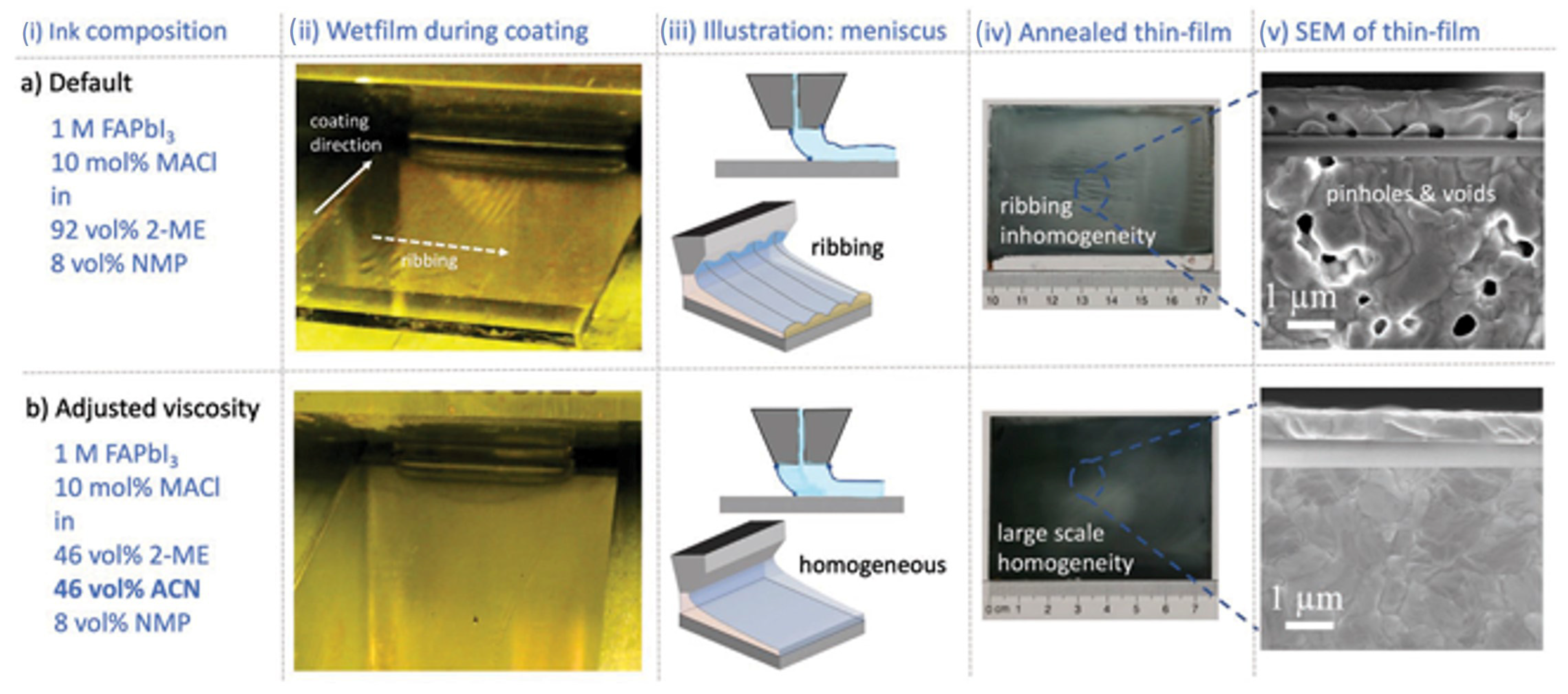
These studies underscore the critical role of ink formulation in achieving high-quality and crystalline perovskite layers, particularly crucial for large-area coatings. Li et al. demonstrated that the solvent composition for perovskite precursors significantly influences the homogeneity and quality of perovskite films deposited by slot-die coating, thereby impacting the performance of large-area PSCs [
59]. It was found that using a mixture of 2-ME and NMP (92:8 vol.%) for dissolving the FAPbI
3 perovskite precursor led to the formation of an uneven perovskite film due to ribbing defects caused by high ink viscosity. Introducing acetonitrile (ACN) as cosolvent reduced the ink viscosity and mitigated the ribbing defects. The optimal ink formulation containing 46 vol% ACN was identified (
Figure 21). Using this optimised ink, the authors fabricated a minimodule (eight sub-cells connected in a series) with an active area of 12.7 cm
2 and achieved an efficiency of 17.1%. The current densities generated by each sub-cell of the module were comparable to those obtained in smaller devices, indicating good homogeneity and quality of the absorber layer.
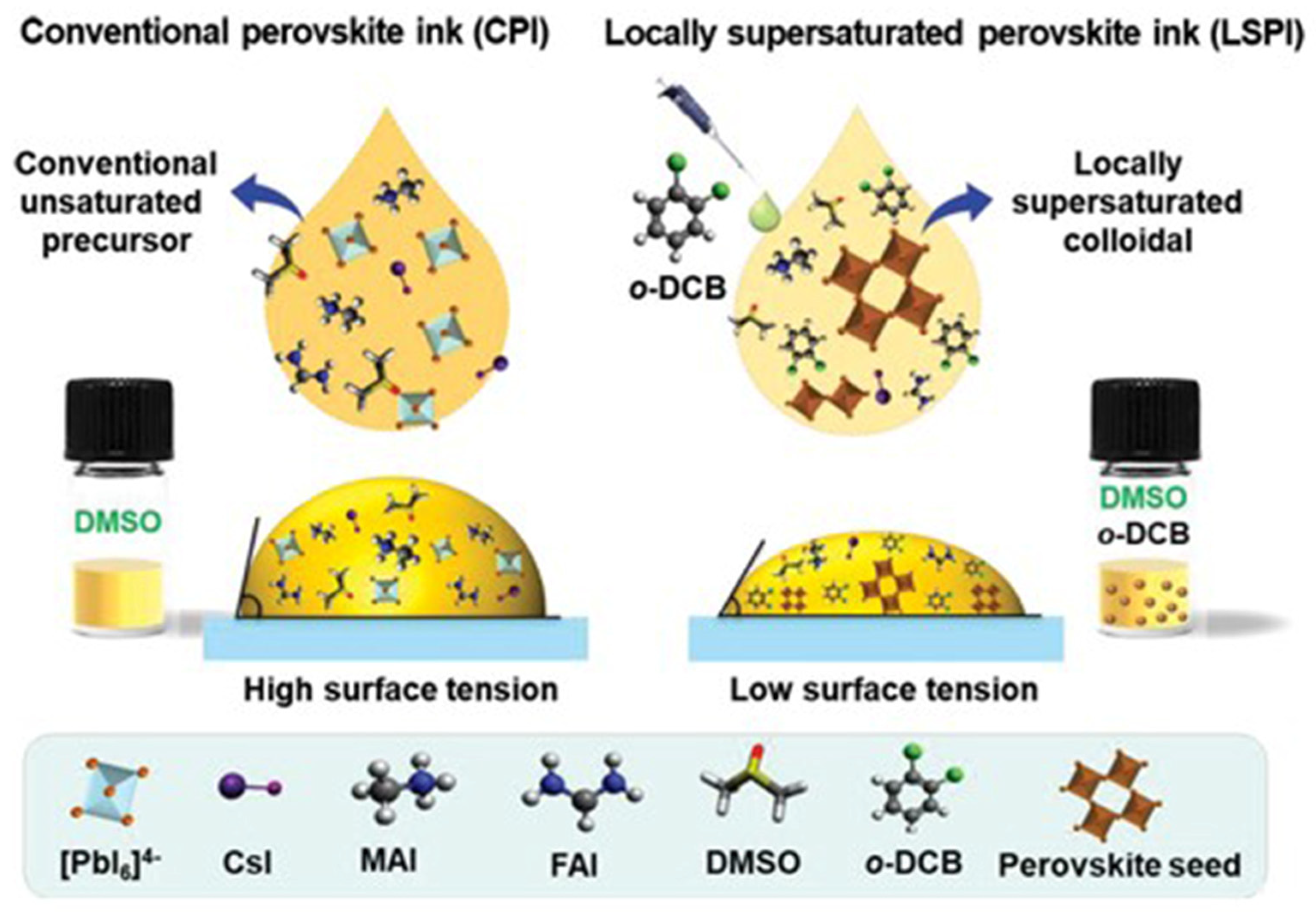
In addition to optimising the viscosity of the perovskite ink, the aim is also to replace the conventional solvents with low-toxicity alternatives suitable for scaling up. Sangale and co-workers added a small amount of 1,2-dichlorobenzene (DCB) into the DMSO-based perovskite precursor to improve the crystal growth of the perovskite layer [
59]. The addition of DCB reduces the ink surface tension and viscosity, facilitating the formation of a uniform wet film and promoting the formation of supersaturated perovskite colloids that act as nuclei for perovskite crystallisation (
Figure 22). This strategy is called engineering-based locally supersaturated perovskite ink (LSPI) and was used to produce the perovskite layer of minimodules by slot-die coating. A PCE of 17.66% was achieved with an active area of 8.64 cm
2. In another work, Abate investigated the effect of different ink-solvent mixtures on the morphology and optoelectronic properties of the perovskite films prepared by slot-die coating [
79]. In addition to the primary solvent (DMSO), a highly volatile solvent such as ACN and 2-ME was incorporated into the CsPbI
2.77Br
0.23 solution precursor. A solvent ratio of 0.8:0.2 (DMSO:ACN) yielded the best-performing PSC devices with enhanced reproducibility, attributed to reduced defects.
Within the topic solvent selection, it is important to consider factors such as viscosity, boiling point, and toxicity. These considerations are crucial not only for their impact on perovskite crystallisation but also for scalability purposes.
4.1.4. Additives and Surface Modification
It has been demonstrated that additives generally improve the performance and stability of PSCs [
80]. Strategies involving alkali metal additives have been shown to modify the trap densities and interfacial defects in spin-coated small-area PSCs, thereby improving crystallisation and reducing hysteresis [
81,
82,
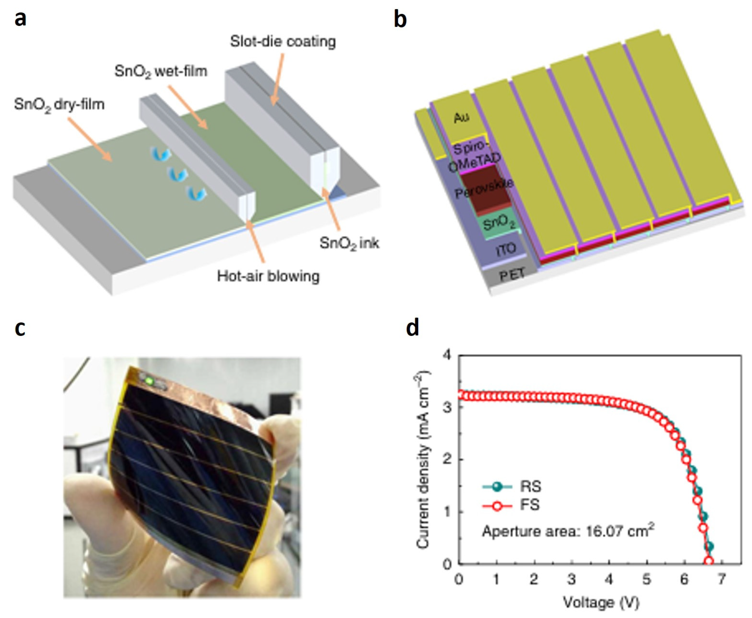
83]. Nevertheless, the role of these additives remains unclear. Therefore, for the fabrication of large-area devices using slot-die coating, it is essential to understand how additives affect the structural and optoelectronic properties of perovskite films. Bu and co-workers investigated the effects of potassium cations on the interfacial passivation between the ETL (SnO
2) and perovskite layer [
43]. They demonstrated that treating the ETL with KOH led to the elimination of hysteresis and improved device performance. It is proposed that potassium ions may react at the surface of the perovskite layer to form KBr. This resulted in the passivation of the halide vacancies at the ETL/perovskite interface, resulting in excellent-performing devices and hysteresis removal. By combining this interface passivation approach with mixed lead halide perovskite cations (MA, FA, and Cs), these authors fabricated a flexible large-area PSC module of 16.07 cm
2 using slot-die coating. A PCE of 14.89% was obtained with negligible hysteresis (
Figure 23).
In a different study, Rana and co-workers investigated how the alkali-based additives CsPbBr
3 and KPb
2Br
5 contribute to the crystallisation of large-area Cs
0.5FA
0.85Pb(I
0.83Br
0.17)
3 (CsFA) perovskite films, along with their effects on the photovoltaic and optoelectronic characteristics [
54]. It was shown that potassium ion segregation occurs at the ETL/perovskite interface, serving as a nucleation site for perovskite film crystallisation. Incorporating these additives into the perovskite ink solution resulted in uniform CsFA films with larger grains and improved optoelectronic properties, ensuring high reproducibility of the device fabrication. A slot-die-coated PSC module with an active area of 57.5 cm
2 was fabricated with a PCE of 16.22%. Moreover, it exhibited excellent stability, retaining 82% of its initial efficiency under 30% relative humidity for 4800 h without encapsulation.
Additionally, Lewis base additives such as diphenyl sulfoxide (DPSO) have been introduced into the perovskite precursor solution to improve the nucleation barrier and stabilise the wet perovskite precursor film on large-area PSC devices [
49]. The use of this additive, together with antisolvent extraction with
n-hexane, allowed the preparation of perovskite films with high quality and reproducibility via slot-die coating. A p-i-n-structured PSC module with a parallel design was prepared, and a certified efficiency of 16.63% was obtained for an active area of 20.77 cm
2. Furthermore, all-organic passivators have shown a facile way to tail steric and electric properties by means of chemical synthesis, structural functionalisation, and rational design [
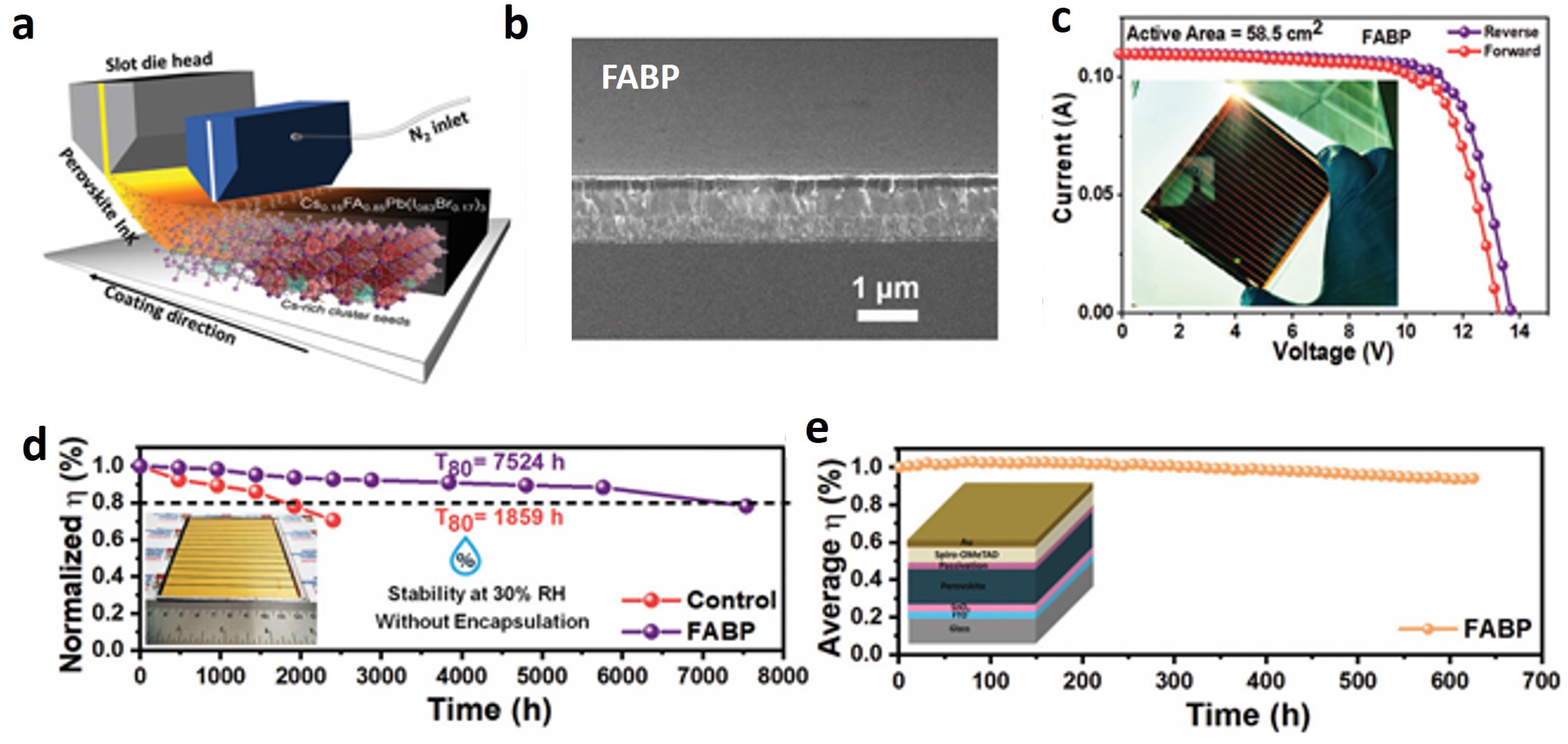
58]. Rana and co-workers introduced an organic passivator, the fluorinated anilinium benzylphosphonate (FABP), to enhance the moisture, thermal, and electrical stability of CsFA perovskite [
58]. The role of FABP was attributed to the defect passivation and inhibition of ion migration by binding to FA site vacancies and undercoordinated Pb ions. For an active area of 58.5 cm
2, the slot-die-coated modules with FABP post-treatment showed a PCE of 19.28% (
Figure 24). Excellent thermal stability was demonstrated by unencapsulated FABP-based modules, which maintained 70% of their initial efficiency at 85 °C for 1700 h. Additionally, under 30% relative humidity, they retained approximately 80% efficiency after 7500 h, and under continuous light illumination, they maintained over 90% of the initial efficiency for over 850 h.
In another study, phenylalanine (Phe), a natural amino acid, was used to control the nucleation and crystal growth process of large-area slot-die-coated FA-based perovskite films [
56]. The addition of Phe resulted in larger grain sizes and improved film coverage. Due to its strong interaction with undercoordinated Pb ions in the perovskite layer, Phe effectively passivates defects and prevents nonradiative recombination. Flexible modules were fabricated on PET/ITO substrates via slot-die coating, where Phe-based devices demonstrated exceptional efficiencies of 12.1% and 11.2% over aperture areas of 185 cm
2 and 300 cm
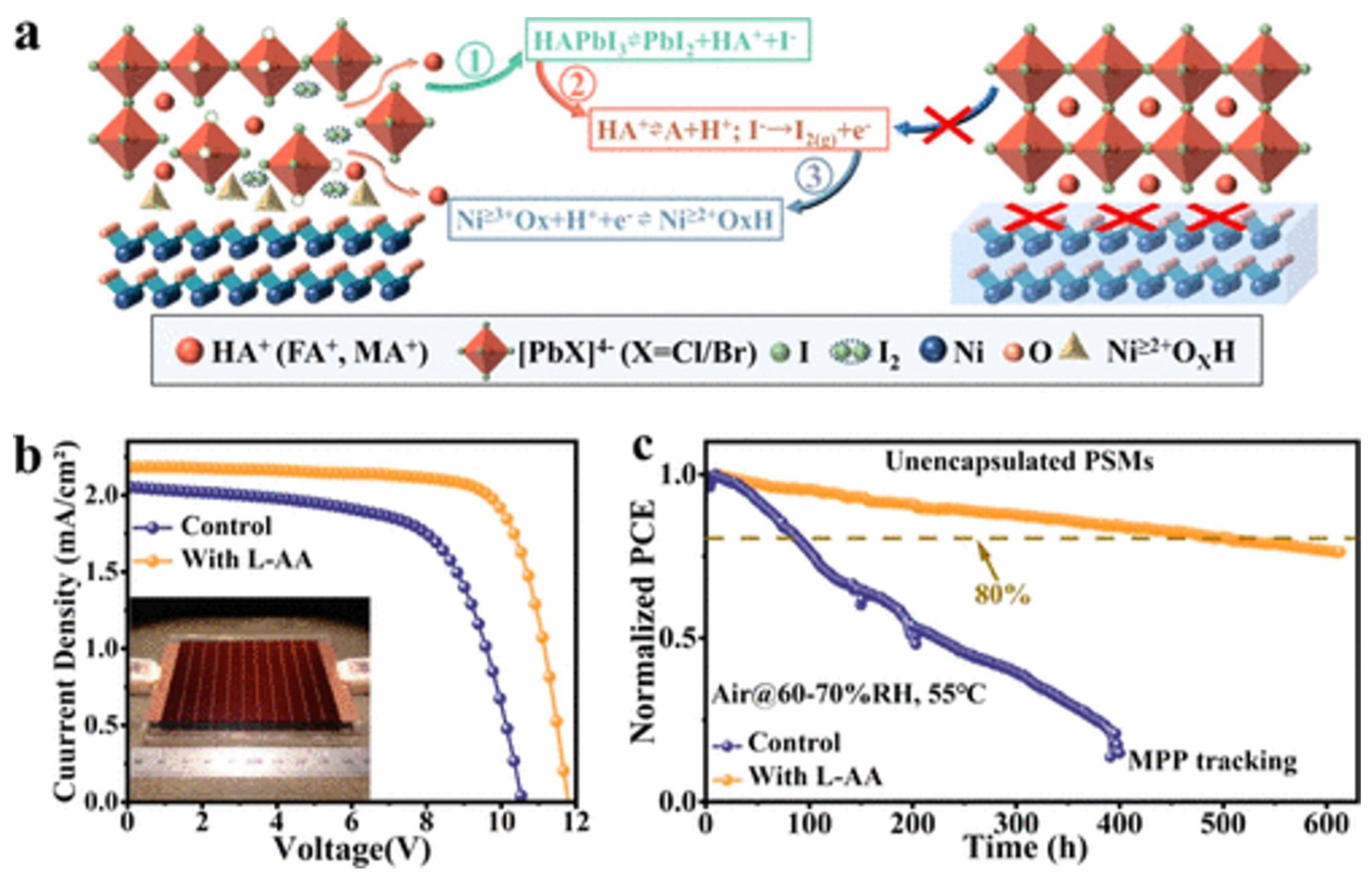
2, respectively. In addition, naturally occurring L-ascorbic acid (L-AA) was added to the perovskite precursor solution to mitigate chemical interfacial reactions of the Ni
≥3+ species between NiO
x ETL and lead cation salts of the perovskite [
64]. These reactions typically introduce additional defects at the NiO
x/perovskite interface, particularly problematic in large-area devices fabricated under air conditions. It was observed that L-AA converts I
2 to I
- in aged solutions and during the interfacial reactions (
Figure 25a). Furthermore, the hydroxyl groups of L-AA inhibit the deprotonation of organic cations, thereby enhancing perovskite layer crystallisation and acting as a barrier layer to prevent an interfacial reaction at the NiO
x/perovskite interface. The coordination of Pb
2+ cations of the perovskite with the C=C and C=O groups of L-AA stabilise the perovskite crystal structure. Utilising this additive, a 10 × 10 cm
2 PSC module was prepared via slot-die coating under ambient conditions, achieving a PCE of 19.17%. Notably, efficiency improvements (from 14.04 to 19.17%) and remarkable stability were also demonstrated (
Figure 25b,c).
Most additives used to improve perovskite morphology are added to the perovskite precursor solution, ensuring their application via slot-die coating alongside the perovskite solution. In this case, these additives directly influence the perovskite crystallisation process, although understanding their precise role can be challenging. Abate and co-workers employed a post-passivation method to modify the defects in slot-die-coated perovskite layers using an artificial amino acid-sulfonyl-γ-AA peptide (F-LYS-S) [
84]. They found that F-LYS-S effectively passivates perovskite defects through multiple interactions involving the -COOH, -C=O, -NH, and -NH
2 groups. Moreover, passivation increased the work function of the perovskite, enhancing the charge extraction and thereby suppressing nonradiative recombination. Large-area (10 × 10 cm
2) regular PSCs prepared with F-LYS-S-passivated perovskite exhibited uniform perovskite layers, as evidenced by UV–Vis analysis at various points, achieving a narrow distribution of PCE values (20.01 ± 0.58%) across the devices. Recently, Rana and co-workers used a benzylammonium iodide (BAI) to passivate slot-die-coated perovskite layers [
63]. The BAI passivation layer was applied at 40 °C and sintered at 100 °C for 1 min, resulting in a larger crystal size and reduced defect density and nonradiative recombination. A three-sub-cell module with a PCE of 14.7% (14.4 cm
2 area) was produced using the proposed strategy.
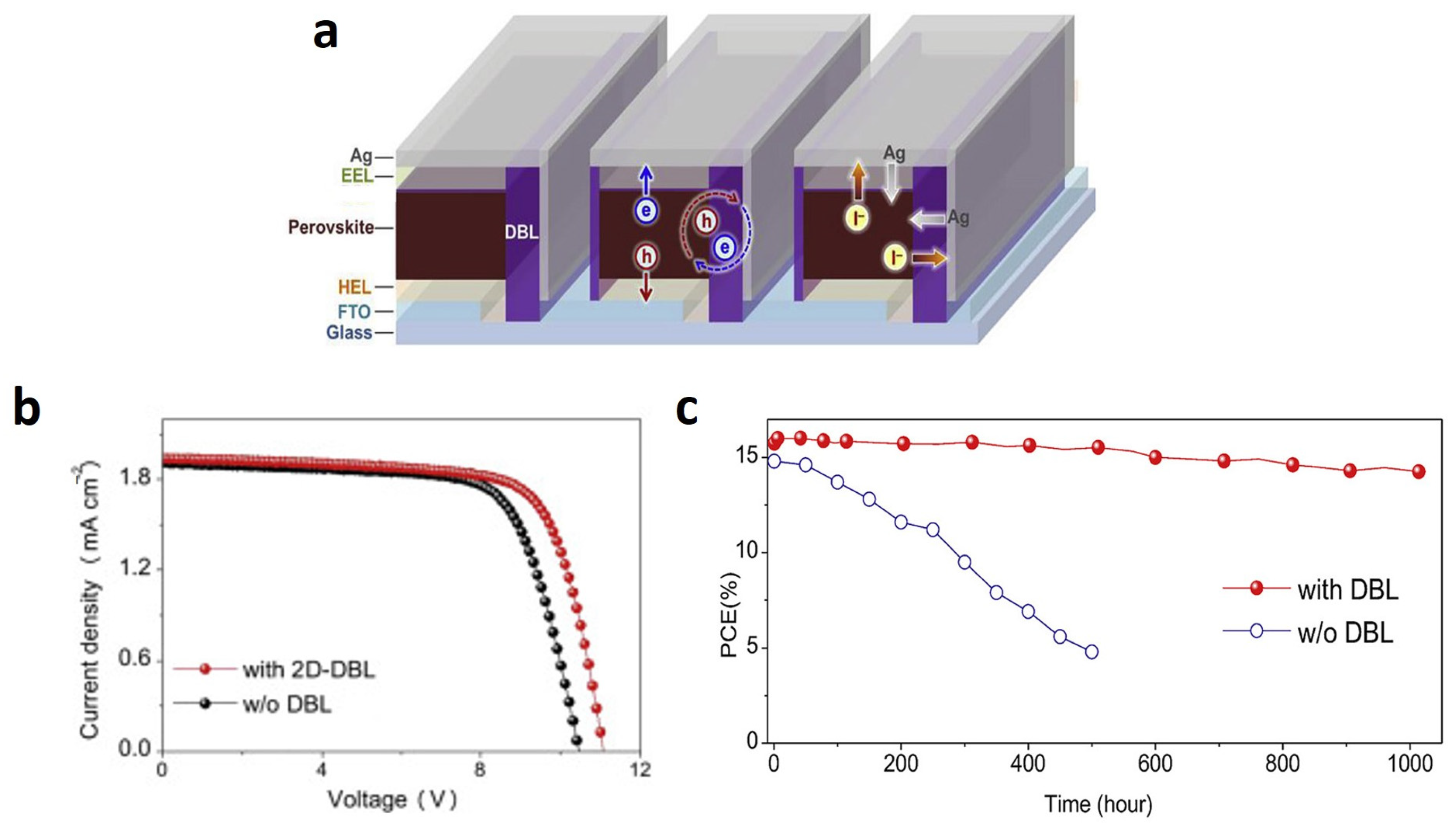
One of the major issues limiting the stability of PSCs is the diffusion of volatile iodide, which leads to irreversible device degradation. To mitigate this issue, Bi et al. introduced low-dimensional diffusion barriers (DBLs) made of inert silicon-based organic polymers, chemically and thermally stable metal oxide nanoparticles, and two-dimensional nanostructured inorganic materials [
44]. They demonstrated that a two-dimensional DBL, a
N-doped graphene fullerene derivative phenyl-C61-butyric acid methyl ester, significantly reduced the iodide leakage rates. Based on these findings, PSC modules with 10 sub-cells connected in a series (36.1 cm
2 of active area) achieved a PCE of 15.6% via slot-die coating for perovskite deposition. A 2D-DBL was strategically placed between the Ag electrode and the perovskite film edge to control lateral iodide diffusion (
Figure 26a). Additionally, DBLs reduced nonradiative carrier recombination at the perovskite surface, thereby enhancing the open-circuit voltage (
Figure 26b) and overall device performance. Even under rigorous testing conditions, the stability of PSC modules was greatly improved by using the 2D-DBL—
Figure 26c.
In conclusion, employing additives to regulate perovskite nucleation is crucial for minimising defects within the perovskite layer, thereby enhancing the device performance. Furthermore, ensuring device fabrication and stability under ambient conditions is critical when aiming for scalability.
4.1.5. Slot-Die Coating Parameters
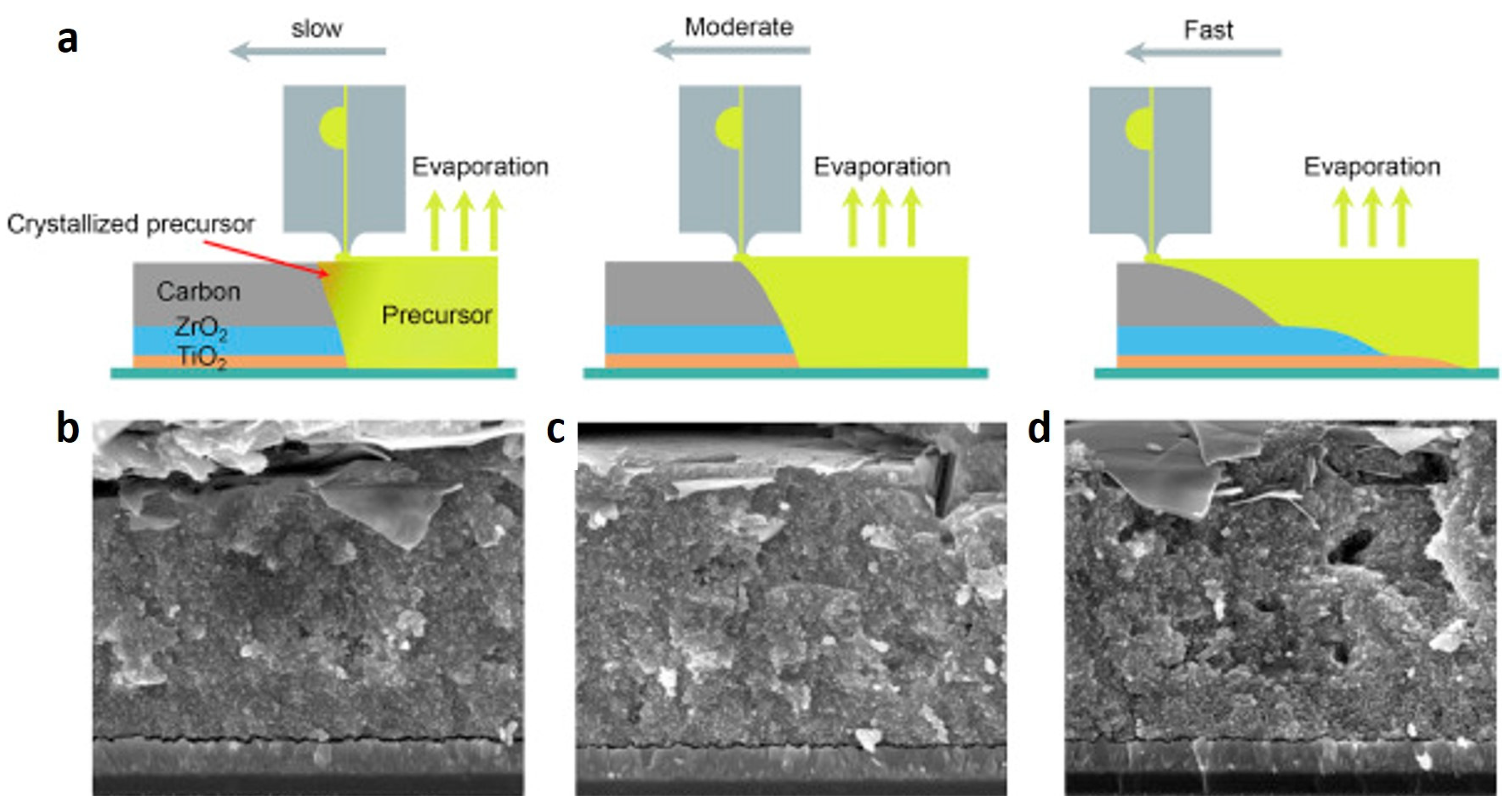
The coating parameters significantly influence substrate wetting and the uniformity of deposited layers. The speed coating, flow rate, and gap distance must be precisely adjusted to achieve homogeneous film deposition in slot-die coating. Xu and co-workers used slot-die coating to apply the perovskite layer on a mesoporous structure [
45]. Adjusting the coating parameters is a complex process, as solvent evaporation competes with perovskite precursor solution infiltration into the mesoporous scaffold (
Figure 27). Capillary forces, coupled with solvent evaporation, facilitate the diffusion and infiltration of the perovskite precursor through the mesopores of the TiO
2/ZrO
2/carbon triple layer, reaching the TiO
2 bottom layer, where perovskite nucleation and growth begin. Higher precursor concentration within the scaffold results from rapid evaporation at the coating edge. On the other hand, slower deposition may lead to solvent evaporation and premature crystallisation of the perovskite precursor, potentially hindering further infiltration. The best-performing PSC module had a PCE value of 12.87% (60.08 cm
2 active area) at a coating speed of 10 mm·s
−1.
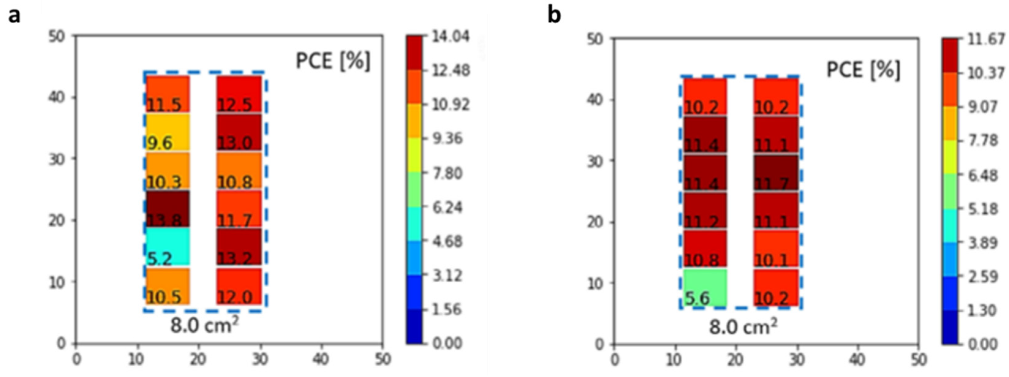
Furthermore, to achieve reproducible slot-die deposition of the perovskite layer on large-area substrates, not only an optimised ink but also a stable meniscus during coating are required. Among all the coating parameters, maintaining a stable flow within the slot-die head has proven to be crucial in preventing ink instabilities that could promote unstable layers and, consequently, inhomogeneous coatings. An ideal geometric design of the slot-die head ensures a uniform flow profile and avoids ink recirculation within the slot-die head. Velásquez and his team used computer fluid dynamics (CFD) simulations to determine the optimal shim thickness required for a uniform velocity distribution of the ink and then experimentally validated the best parameters [
85]. These optimised coating parameters enable the formation of a continuous wet film on the substrate. PSC minimodules, comprising 12 sub-cells of 0.4 cm
2 each, totalling 8 cm
2, were fabricated via slot-die coating. The efficiencies of these modules were compared with those of spin-coated devices. In contrast to spin-coated devices, which showed poor reproducibility and lower efficiencies, the slot-die-coated devices demonstrated consistent efficiency across individual cells within the module, showcasing excellent reproducibility over large areas (
Figure 28).
Recently, Peng and co-workers used CFD simulations to investigate how the formation of perovskite films when using low-viscosity inks is affected by the upper and lower coating limits, as well as the flow field’s stabilisation [
86]. These theoretical studies were then validated with experimental data. The findings indicated that a coating speed 0.7 times higher than the maximum speed of the Poiseuille flow component is required for successful coating.
In summary, optimising the slot-die coating parameters, such as coating gap and speed, ink flow rate, and slot-die head design, is crucial for controlling the thickness and morphology of the perovskite film on large-area substrates.
4.1.6. Mixed Strategies
Depositing hydrophilic perovskite inks on the hydrophobic surface of PTAA, the most used HTL in p-i-n PSCs, via slot-die coating has proven to be very difficult, often resulting in nonuniform perovskite layers. To circumvent this problem, Subbiah et al. combined three main strategies: solvent engineering, surfactant additives to enhance ink-wetting, and interfacial passivation to prepare efficient p-i-n PSCs using the slot-die coating technique [
47]. They showed that factors such as ink–substrate kinetics and solvent properties, which affect the drying process and crystallisation rate, are critical for producing high-quality slot-die-coated devices. First, low boiling point acetonitrile was added to a methylamine/methanol mixture to replace the conventional solvent (DMF) used to prepare the MAPbI
3 perovskite solution. This solvent system ensures rapid solvent evaporation and lowers the substrate temperature from approximately 150 °C to 70 °C, both essential for quick crystallisation without antisolvent extraction. Second, L-α-phosphatidylcholine (LP) was included as a surfactant to improve the wettability and contact with the hydrophobic PTAA HTL. The addition of a LP additive resulted in larger grain size, more uniform perovskite films, and reduced roughness. Third, cysteine hydrochloride (Cys.HCl) was used to passivate the perovskite MAPbI
3 surface, reducing open-circuit voltage losses. By combining these strategies and using slot-die coating, PSC modules with an active area of 6.8 cm
2 and a PCE of 14.4% were fabricated.
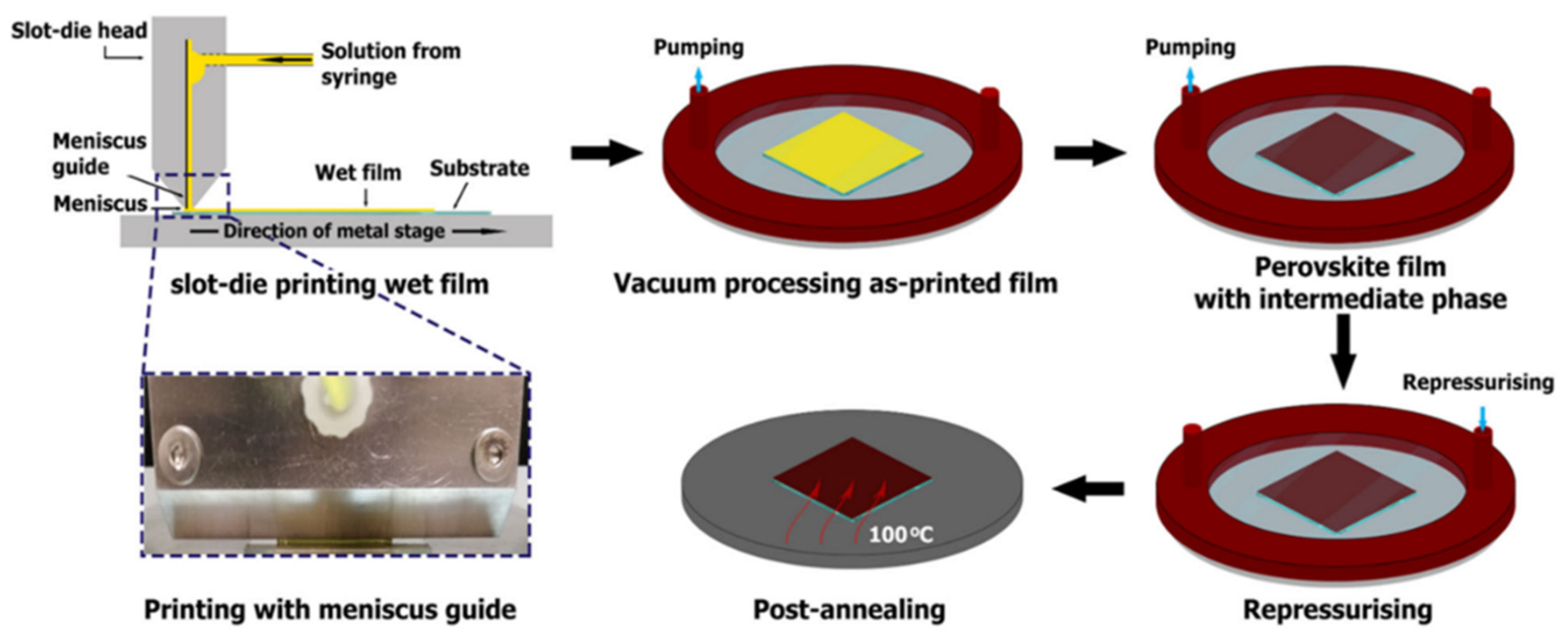
Another study focused on the use of vacuum quenching and Cl additives, such as MACl and FACl, to control perovskite film crystallisation [
52]. The addition of Cl additives resulted in highly crystalline and smooth perovskite films with large grains. The vacuum quenching was shown to be crucial for the formation of the perovskite intermediate phase, resulting in a good crystallisation and well-controlled removal of solvents (
Figure 29). It also benefited the morphology of the PCBM (ETL) and BCP layers. The corresponding slot-die-coated PSC modules with 2.1 cm
2 of active area showed a PCE of 14.9%.
More recently, Vesce et al. fabricated large PSC modules in ambient air by slot-die coating, where the deposition of the perovskite layer was assisted by air quenching and antisolvent strategies [
62]. Additionally, they implemented a perovskite passivation strategy using phenethylammonium iodide (PEAI), together with a low-boiling solvent, ACN, to the perovskite precursor solvent mixture to enhance the homogeneity of the perovskite layer. This combined approach suppressed nonradiative recombination and improved the extraction of the charge at the charge transport layer (CTL)/perovskite interface. The use of ACN also resulted in better quality and nucleation of the perovskite layer. The high homogeneity of the perovskite layer enabled a PCE of 16.1% for a PSC module with 186 cm
2 active area.
4.2. Charge Transport Layers
In addition to the strategies reported for controlling the morphology of the perovskite layer during its deposition, the material used as the charge transport layer below the perovskite layer also influences the quality of the perovskite crystals and the overall performance of the PSC devices. For this reason, CTLs should be chosen wisely, considering their charge selection ability, transparency, energy level alignment, environmental tolerance, and substrate compatibility. Concerning this topic, several works will be reviewed next.
4.2.1. Electron Transport Layers
In the n-i-p PSC architecture, TiO
2 is the most commonly used electron transport layer. This ETL has an energy level well aligned with the perovskite layer and exhibits excellent electron extraction capability [
87]. Additionally, TiO
2 serves as a scaffold for the formation of the perovskite layer [
88]. The deposition of TiO
2 using slot-die coating was first demonstrated by Burkit et al. [
89]. They deposited compact TiO
2 (
c-TiO
2) from a dilute methanolic solution of titanium diisopropoxide bis(acetylacetonate) and dried it at 105 °C. The devices fabricated with this compact TiO
2 layer showed better performance than the spin-coated devices (structures A and B,
Table 2) due to a higher short-circuit current density (
JSC) and fill factor (FF), which resulted from better surface coverage. Furthermore, the mesoporous TiO
2 layer (
m-TiO
2) was prepared by slot-die coating a dilute solution of DSL-18NRT titanium dioxide paste and sintering it at 550 °C. SEM analysis showed that slot-die-coated films were more uniform and flatter on the substrate compared to the spin-coated films, which exhibited striation defects and a rough surface (
Figure 30). Complete devices with the
m-TiO
2 layer produced by slot-die coating (structure C,
Table 2) were compared with the spin-coated devices (structure B,
Table 2). Despite an increase in the open-circuit voltage (
VOC), the slot-die-coated
m-TiO
2 devices performed worse, mainly due to the decrease in
JSC, ascribed to the inferior uniformity of the perovskite layer.
While these results suggest that slot-die coating is suitable for producing mesoporous TiO
2 and can even enhance the film quality, the need for high sintering temperatures (>450 °C) renders the scaling up of devices impractical. Alternatively, low-temperature TiO
2 processes have been reported. For instance, TiO
2 nanoparticles in the anatase phase enable the preparation of a highly uniform TiO
2 layer at 100 °C by slot-die coating [
90]. Additionally, rutile nanoparticles derived from the hydrolysis of TiCl
4 at 70 °C in a chemical bath offer another low-temperature option [
91].
Other promising alternatives to TiO
2 ETLs include tin oxide (SnO
2) and zinc oxide (ZnO). In recent years, SnO
2 has been widely employed as ETL in large-area PSCs prepared by slot-die coating. The most successful process involves the deposition of a colloidal SnO
2-water dispersion, followed by thermal annealing at 150 °C [
43,
78,
92], as proposed by Bu et al. [
43]. The rapid drying promoted by the air knife prevents aggregation of the SnO
2 crystals and forms a smooth and compact layer. Notably, the PSC devices fabricated with this ETL showed no hysteresis. Investigations revealed that the strong basicity of the aqueous colloidal SnO
2 dispersion, due to K ions in the solution, passivates the interface between SnO
2 and perovskite, thus eliminating hysteresis. The champion PSC module prepared with these SnO
2 nanoparticles achieved a PCE of 14.89% for an aperture area of 16.07 cm
2. Vijayan and co-workers examined the film quality of two commercial SnO
2 dispersions: a water-based dispersion (W-SnO
2) and a butanol-based dispersion (B-SnO
2), both deposited by slot-die coating [
93]. They discovered that, although controlling the W-SnO
2 dispersion was more challenging, the devices performed better. By carefully optimising the parameters of the slot-die coating, a PCE of 17.5% was achieved for a MAPI-based PSC. The main difficulty with water-based SnO
2 nanoparticles is the high surface tension, which typically leads to the formation of large pinholes due to dewetting during slot-die deposition. To prevent dewetting, plasma and ozone substrate treatments are commonly used, even if these methods require expensive equipment. As an alternative, low-surface tension solvents, such as isopropyl alcohol (IPA), have been used to prevent dewetting [
94]. The addition of IPA improved wetting and increased the aggregation of SnO
2 nanoparticles, resulting in a smooth SnO
2 film.
ZnO is another alternative to TiO
2; however, because of its thermal instability, it has received less attention. However, the low-temperature annealing of their nanoparticles (100–120 °C) is attracting interest. Khambunkoed and co-workers demonstrated that the PSC performance depends on the thickness of the ZnO layer [
95]. They found that the film thickness (
d) is related to the slot-die coating speed (
S), according to the following expression:
d α
S0.667. Films that are too thin have pinholes, leading to current leakage and recombination, while films that are too thick have a lower electron extraction efficiency. The optimal performance was obtained for ZnO films with a thickness of 38 nm. The ZnO layers produced with the optimised slot-die coating parameters were compared with the spin-coated layers. It was found that slot-die films exhibited better coverage and uniformity on the FTO substrates, resulting in the better performance of the fabricated PSC devices. The ZnO-based PSCs prepared using slot-die coating achieved a PCE value of 10.81% compared to 9.96% for spin-coated PSCs, which is due to the lower charge recombination.
In summary, while TiO2 has the largest electron extraction capacity among ETLs, the high-sintering temperatures required for the most common precursor formulations limit scalability. TiO2 nanoparticles may be an alternative, though their UV sensitivity poses a challenge for long-term stability. Compared to the other proposed alternatives, ZnO and SnO2, the latter could be a strong candidate to replace TiO2 if its charge extraction ability is improved.
4.2.2. Hole Transport Layers
In p-i-n devices, the HTL plays a crucial role in the formation of the perovskite layer, with PEDOT-PSS being the most commonly used material. PEDOT-PSS offers good electrical conductivity and light transmittance and is compatible with R2R deposition processes, making it suitable for large-area devices. However, its acidity and hygroscopicity can compromise the stability of PSC devices, and its mismatched energy band alignment with the perovskite layer leads to voltage losses. The use of additives can improve PEDOT:PSS properties; for instance, adding polymer electrolyte PSS-Na increases its work function, aligning it better with the perovskite layer and enhancing the voltage and power conversion efficiency [
96]. This modified PEDOT:PSS has been used to fabricate large-area PSC devices via slot-die coating, showing good surface coverage [
97,
98]. Despite these improvements, alternative materials are being explored. PTAA and poly-TPD are used for PSC fabrication by slot-die coating, offering excellent electrical properties, low processing temperatures, and high open-circuit voltages (>1 V). However, their hydrophobic surface can lead to wettability problems, especially when using polar solvents like DMF or DMSO for the perovskite precursor solution, leading to defects and nonuniform perovskite films. Bisconti and co-workers addressed this issue by treating the poly-TPD surface with mild oxygen plasma before perovskite deposition, reducing the contact angle from 62° to 45° [
99]. In PTAA, high surface hydrophobicity challenges slot-die coating due to solution flow dynamics, causing adhesion problems with the perovskite layer [
100,
101]. Adding surfactants to the perovskite precursor solution can mitigate this by altering the ink’s drying dynamics and increasing adhesion [
47,
102].
Copper thiocyanate (CuSCN) has emerged as a cost-effective and reliable HTL material. Zimmermann et al. reported for the first time the deposition of this HTL material by slot-die coating, using methyl ethyl sulphide as a cosolvent to enhance the solubility. This optimised ink enabled uniform CuSCN layer deposition on 5 × 10 cm
2 substrates and the fabrication of 9 cm
2 PSC minimodules with a PCE value of 14.7% [
103].
Despite the advantages of organic HTLs in charge extraction and processing, their high cost limits their scalability. Inorganic materials like NiO
x and graphene oxides (GOs) offer more attractive alternatives. NiO
x, in particular, matches the perovskite material’s energy level better, resulting in higher
VOC values. It can be produced by a sol–gel process or from a prefabricated nanoparticle ink, both requiring low sintering temperatures for slot-die coating. Huang and co-workers reported large area (12 × 12 cm
2) NiO
x HTL layer deposition via slot-die coating using a nickel acetate sol–gel solution, with drying and crystallisation achieved using a near-infrared lamp [
46]. Wang used NiO
x nanoparticles to prepare a uniform layer on 1.01 cm
2 rigid PSC devices, subsequently treating the layer with HI solution to improve the device performance from 17.86% to 20.51% [
104]. This strategy was also applied to flexible PSC modules, achieving a PCE of 16.15% (15 cm
2). In another work, the NiO
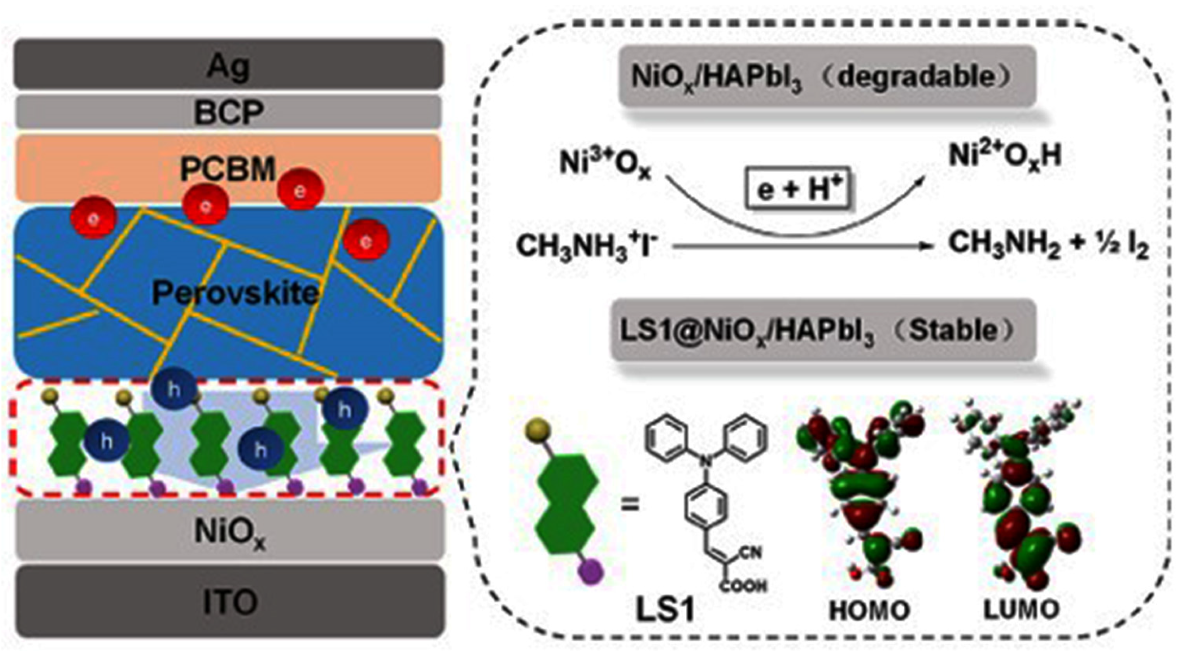
x/perovskite interface was passivated with a self-assembled donor–acceptor dyad molecule (named LS1), improving both performance and stability. The LS1 molecule enhances charge extraction at the HTL/perovskite interface and promotes perovskite crystal growth (
Figure 31). This approach resulted in a PSC module with an aperture area of 19.16 cm
2 and a PCE value of 14.90% using slot-die coating [
105].
A surface redox engineering (SRE) process has been proposed as an alternative approach to the use of additives for NiO
x films [
57]. In the first step, the NiO
x film is exposed to a nonthermal Ar-plasma environment, which improves the surface wettability. In the second step, the films are treated with a Brönsted acid (nitric acid), facilitating the reduction of NiO
x by eliminating Ni
4+ and neutralising the surface hydroxyl groups. The SRE method for NiO
x films significantly reduces pinholes and promotes larger perovskite crystal growth, resulting in a compact and uniform perovskite layer. The scalability of the SRE approach for PSCs was demonstrated by fabricating a large-area module (174 cm
2 active area) that achieved a PCE of 18.6%, where the perovskite layer was prepared by slot-die coating.
Reduced graphene oxides (rGOs) are a less common HTL material but with very interesting properties. They can be functionalised to modulate their properties and serve as a scaffold for crystalline perovskite film growth. Jung et al. [
106] demonstrated that replacing PEDOT:PSS HTL with fluorinated reduced graphene oxides (F-rGOs) in a fully slot-die-coated PSC device resulted in a higher PCE (12.52% vs. 9.57%), mainly due to the improved
VOC and
JSC.
Indeed, optimising the charge transport layer beneath the perovskite material (ETL for n-i-p devices or HTL for p-i-n devices) is of great importance for the fabrication of large-area PSC devices. Several considerations include (i) ensuring adequate wettability of the charge transport material for optimal surface coverage, crystallisation rate, and perovskite film quality; (ii) aligning the CTL energy level with the perovskite material to enhance the charge extraction and inhibit charge recombination at the CTL/perovskite interface; (iii) minimising defects at the CTL/perovskite interface to reduce VOC losses and improve device performance; (iv) ensuring compatibility with the perovskite material to prevent degradation; and (v) employing low-temperature deposition processes suitable for scalable production, preferably compatible with R2R processes.
5. Advancements in Roll-to-Roll (R2R) Slot-Die Coating
The R2R coating process imposes specific requirements and constraints on the materials and substrates that can be used. Flexible substrates are essential for high-throughput production, necessitating materials that can be processed at low temperatures (<140 °C). This requirement excludes mesoporous perovskite solar cells due to the high sintering temperatures required for TiO
2 layers (450 °C) [
107]. Therefore, achieving highly efficient R2R-processed PSCs involves considering three critical aspects: (1) using a scalable deposition technique for the active perovskite layer that is compatible with R2R processing, (2) fabricating PSC devices on flexible substrates requiring low processing temperatures (<140 °C), and (3) ensuring the back electrode is deposited effectively to establish good contact with the active material without damaging the underlying layers.
Schmidt and co-workers reported a fully scalable R2R-compatible fabrication process for PSCs under ambient conditions, marking a significant advancement [
108]. Their approach involved three key steps: first, replacing the rigid glass substrate with a flexible PET substrate; second, the perovskite solar cell stack was prepared via a R2R process using a slot-die coater; and third, the evaporated back electrode was replaced by a screen-printed back electrode. Detailed investigations revealed a 50% reduction in performance for both regular and inverted PSC architectures, highlighting the sensitivity of scaling to substrate changes. The study underscored the critical influence of ink formulation and sintering methods on back electrode deposition, with inverted PSC structures showing greater resilience to these challenges. Despite the initial setbacks, this research demonstrated the feasibility of scaling PSCs onto flexible substrates under ambient conditions using scalable deposition techniques like slot-die coating, paving the way for future developments.
Subsequent studies have explored R2R slot-die processing for layers other than the perovskite layer in PSC device stacks, encompassing both inverted and regular PSC structures. However, challenges remain, as back electrodes are still typically applied offline. One- and two-step procedures have also been used for R2R processing of the perovskite layer, such as the two-step approach used by Burkitt for the perovskite layer deposition, in which ethanol was used as a solvent for the MAI ink solution and DMSO as a solvent for the PbI
2 ink. An inverted PSC with the structure PET/ITO/PEDOT:PSS/MAPbI
3/PCBM/BCP/Ag was fabricated using R2R slot-die coating for preparing the HTL and perovskite layers [
36]. The champion device achieved a PCE of 9.4%, but challenges arose from the high temperature required to dry the wet film containing the low-volatile DMSO-PbI
2 ink, which damaged the PET substrate and caused significant variations in the performance of the devices. This highlights the urgent need for developing solvent systems that enable low-temperature drying, thereby enhancing the crystallisation and overall device performance. To improve the morphology and quality of MAPbI
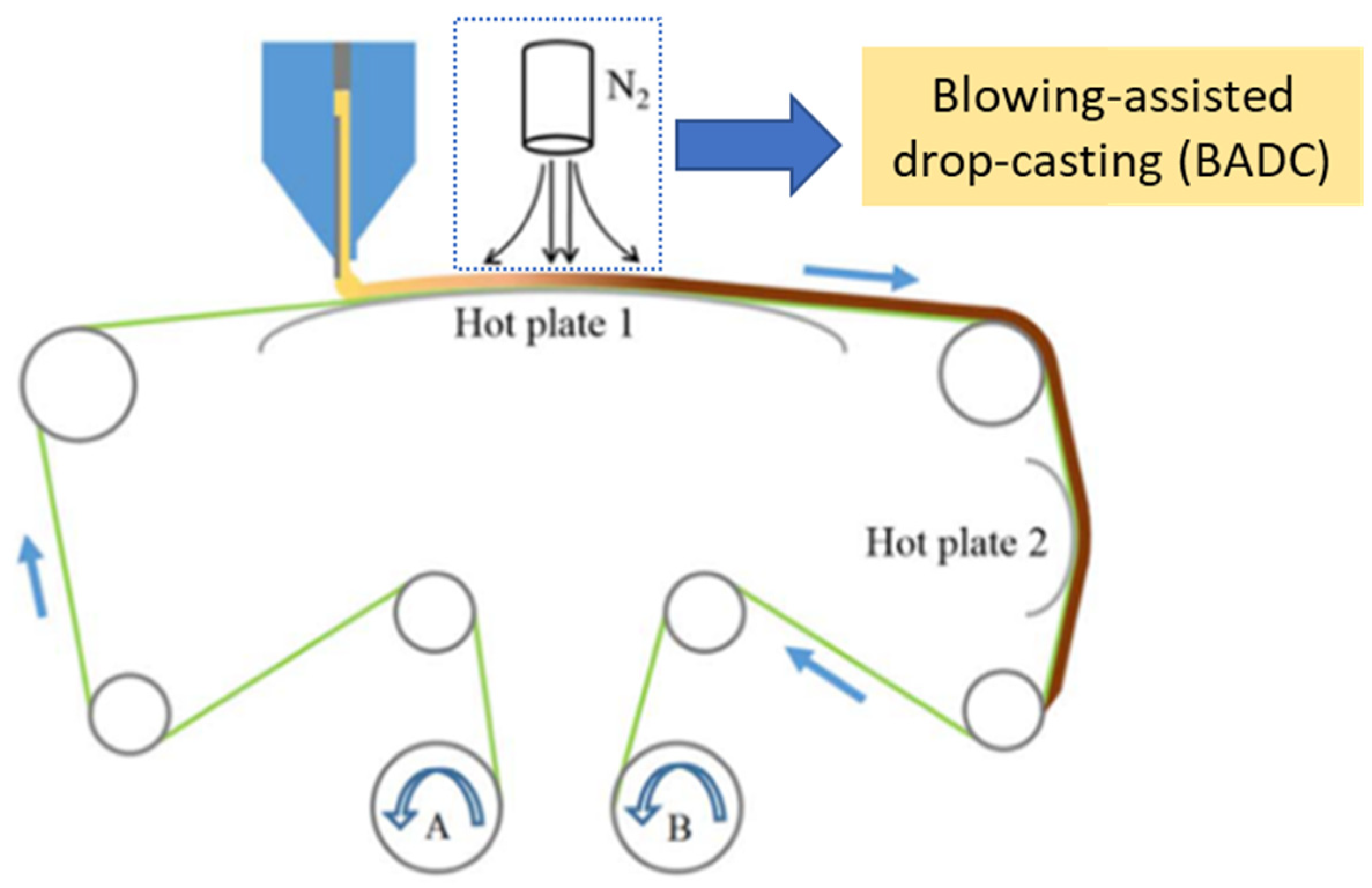
3 films in PSCs, Zuo reported a blowing-assisted drop-casting (BADC) approach compatible with R2R processing (
Figure 32). This method created a dry atmosphere around the substrate during MAPbI
3 film nucleation, preventing water ingress and resulting in superior film morphology. The addition of NH
4Cl significantly enhanced the film crystallinity and morphology, leading to improved device performance. The PSC device with the structure ITO/PEDOT:PSS/MAPbI
3/PCBM/Ca/Al had a maximum PCE of 11.16%. However, R2R slot-die coating remains limited to the HTL and perovskite layers in current applications.
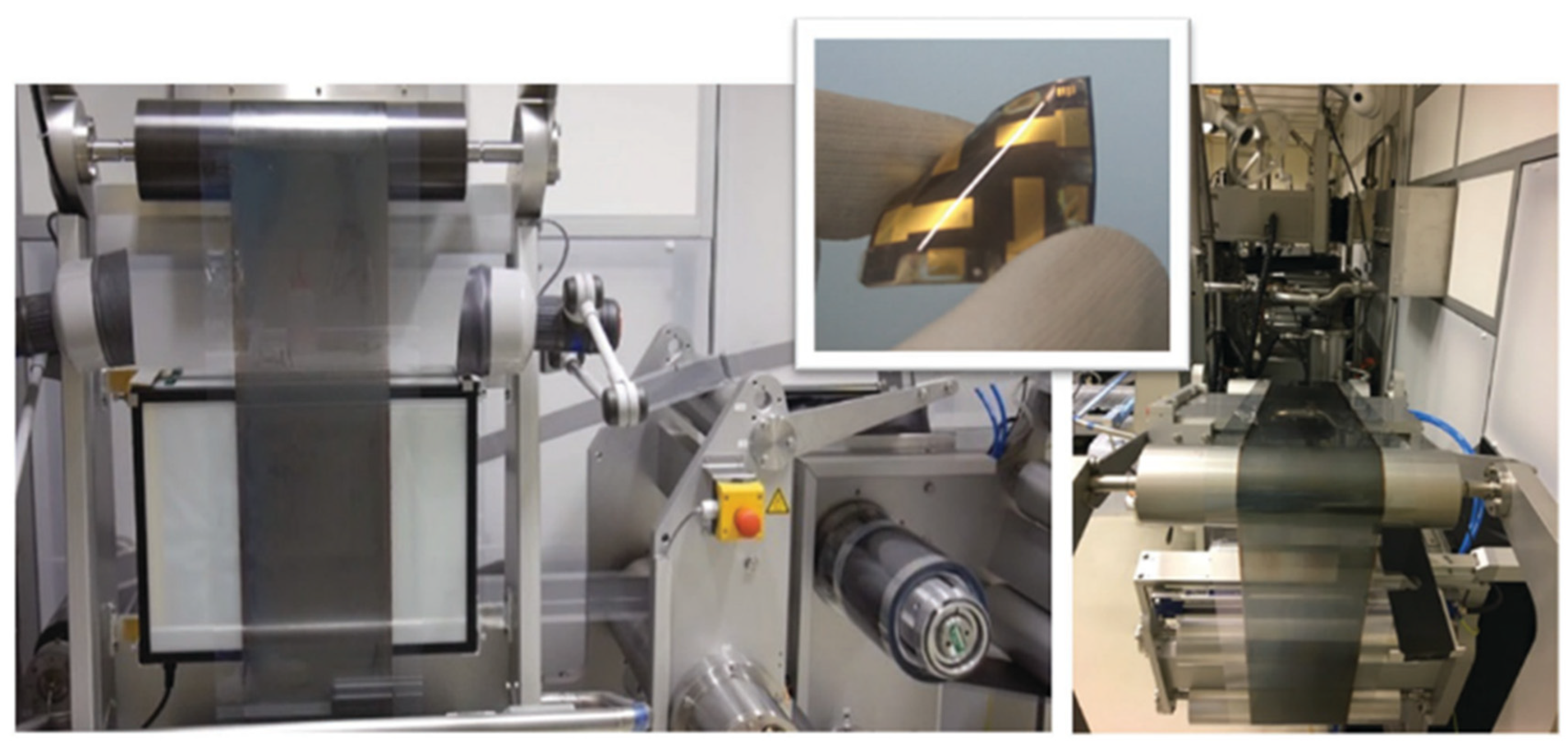
As previously mentioned, in addition to the perovskite layer, other active layers such as the ETL have been also prepared using R2R slot-die coating. Galagan showed that, under ambient conditions (RH 60% and 25 °C), R2R slot-die coating of both the ETL (SnO
2) and perovskite layers was achievable over large areas on flexible substrates (30 cm width)—
Figure 33 [
109]. Following the R2R procedure, segments of the PET foil were cut from the PET/ITO/SnO
2/perovskite roll. For device fabrication, the HTL (spiro-OMeTAD) was spin-coated onto these segments before the thermal evaporation of the Au back electrode. In an alternative approach, slot-die coating was used instead of spin-coating for depositing the spiro-OMeTAD HTL, yielding a comparable performance and thereby demonstrating its integration capability into the R2R process without compromising the PSC performance. The resulting planar PSC device achieved an efficiency of 13.5% (0.09 cm
2).
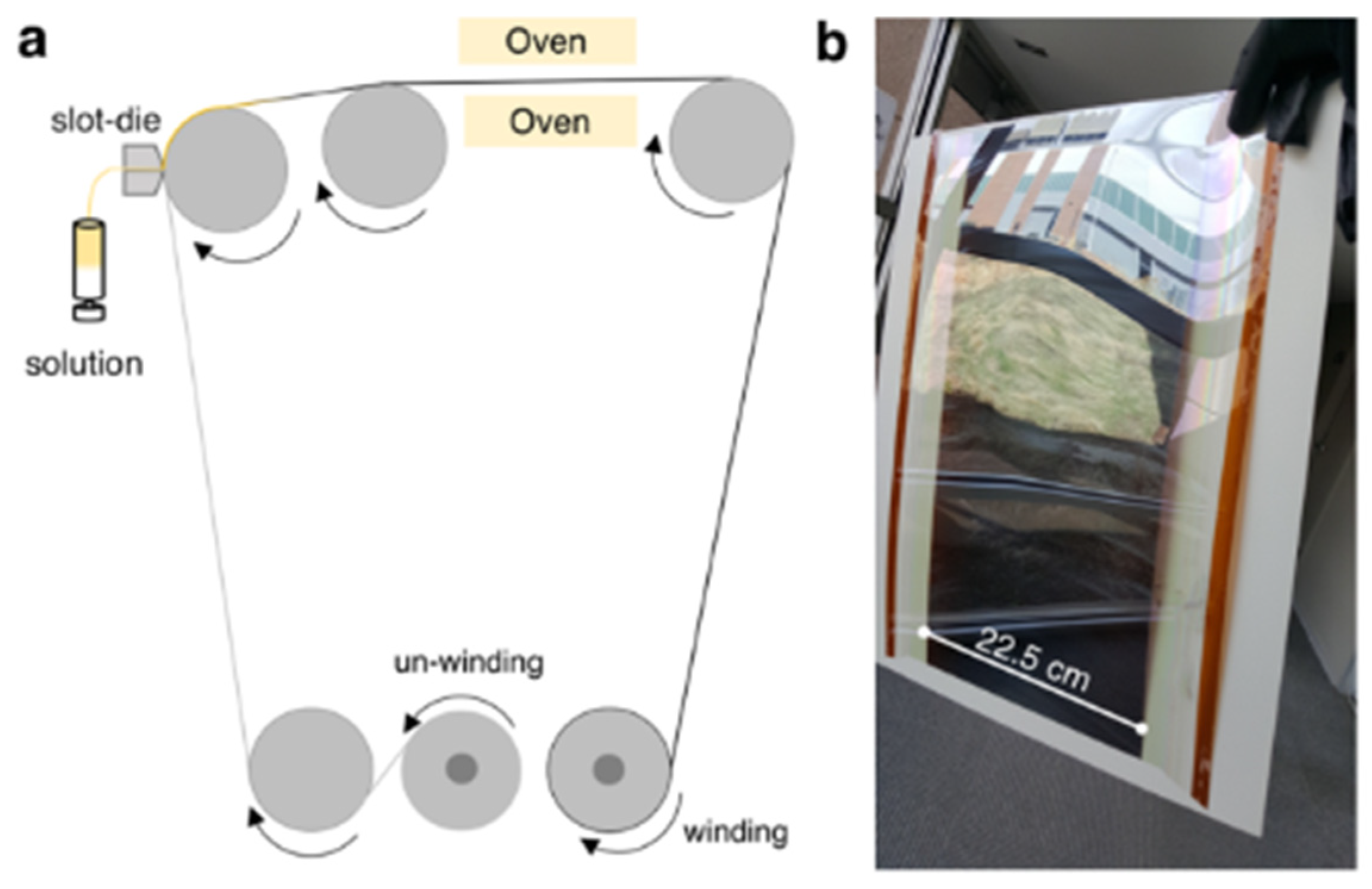
Dou and co-workers also used R2R slot-die coating for preparing both SnO
2 ETL and perovskite layers on a flexible glass substrate under ambient conditions [
110]—
Figure 34. The perovskite layer was formed using a precursor solution comprising acetonitrile:methylamine, facilitating rapid crystallisation of the perovskite films and enabling R2R fabrication at room temperature. Following R2R coating, the perovskite films were divided into square pieces, spin-coated with spiro-OMeTAD, and the devices finalised with Au thermal evaporation. An efficiency value of 14.1% was achieved. Furthermore, the study demonstrated that these deposition conditions are not limited to the MAPbI
3 perovskite material but can also be extended to other perovskite compositions, such as FA and Br systems.
Despite the enormous potential of R2R for scaling PSCs, the efficiency of devices fabricated using this method still lags behind that of devices produced on rigid substrates via slot-die coating. One of the limitations of R2R processing is the restricted flexibility in adjusting the coating parameters, while the processing times and temperatures are major constraints, particularly when using polymer substrates. Kim et al. [
97] used a heated deposition approach to fabricate PCSs via R2R slot-die coating under ambient conditions. They demonstrated that heating the coating bead to 130 °C without gas blowing enables the formation of high-quality perovskite layers with large crystals. This approach was applied to fabricate inverted PSCs entirely coated using R2R slot-die coating, with a structure of PET/ITO/PEDOT:PSS/perovskite/PCBM/PEIE/Ag, achieving a PCE of 11.7%. Later, a similar high-quality perovskite film was obtained with the structure OPV8/SnO
2/FA
0.91Cs
0.09PbI
3/spiro-OMeTAD/Au, incorporating FEAI as an additive to the perovskite layer and conjugating a N
2 flow with thermal annealing [
111]. Except for the back electrode, which was thermally evaporated, the entire PSC device was slot-die-coated in a R2R process, and a PCE of 15.4% was achieved.
The two-step perovskite deposition method, known for improving the perovskite layer morphology in slot-die deposition, has also proven effective in R2R processes. Hwang and co-workers [
38] fabricated regular PSCs in a R2R slot-die deposition process, using the two-step perovskite film deposition method to prepare PSCs with the PET/ITO/ZnO/MAPbI
3/P3HT/Ag configuration (
Figure 35). To form uniform and dense films, a PbI
2 solution was first deposited on the flexible PET/ITO/ZnO substrate and dried under N
2. Subsequently, the perovskite layer was formed by coating the PbI
2 layer with a MAI solution. Despite initial challenges resulting in a low PCE (≈1%) for a 10 × 10 cm
2 module, due to difficulties in achieving high-quality perovskite layers over large areas, subsequent improvements were made by Heo, who introduced a PbI
2:MAI (1:0.4) mixture in the first perovskite deposition step [
112]. MAI acts as an additive, retarding the crystallisation of PbI
2. An unstable intermediate phase was generated, facilitating the rapid conversion to perovskite upon MAI coating (second step in the perovskite deposition). As a result, the homogeneity of the perovskite film increased, and a PCE of 11% was attained. Li and co-authors further enhanced the perovskite crystallinity and morphology by optimising the N
2 flow and substrate temperature [
113]. They used a two-step sequential procedure for the perovskite layer deposition, initially slot-die coating PbI
2:CsI, followed by an organic cation solution, demonstrating a R2R slot-die coating under ambient conditions. The resulting porous PbI
2:CsI layer promoted rapid and complete conversion into a perovskite film, resulting in a PSC device with a structure PET/ITO/SnO
2/MAPbI
3/spiro-OMeTAD/Ag, achieving a PCE of 13%.
The two-step perovskite deposition method has proven to be effective in enhancing the perovskite film quality, but its integration into a R2R process presents significant challenges. The high temperatures required for sintering the PbI
2 layer and the long sintering time pose risks to the integrity of the polymer substrates and can reduce the production rate. Park and co-workers introduced a novel annealing technique known as intensive pulse light (IPL) to achieve the rapid conversion of PbI
2 into perovskite crystals [
114]. Following R2R deposition of the SnO
2 ETL, a PbI
2 solution was deposited using the same R2R process and dried with an air stream. In a second step, the FAI precursors were deposited on the PbI
2 layer and annealed with the IPL (
Figure 36). These authors also showed that the addition of cesium formate and cesium iodide to the PbI
2 solution improved the device efficiency. Moreover, an enhanced quality of the perovskite layer was achieved by following IPL with a 2 min sintering process at 150 °C, which significantly reduced hysteresis. This dual-sintering approach resulted in a PCE of 11.25% for a 10 × 10 cm
2 module with an active area of 94.6 cm
2 (20 sub-cells).
Within the Solliance Consortium, Giacomo customised the ink formulation and drying procedure to control the perovskite crystallisation, thereby preventing efficiency losses during the upscaling of PSC devices with the structure ITO/SnO
2/perovskite/spiro-OMeTAD/Au [
42]. The perovskite layer was deposited using R2R slot-die coating, resulting in a flexible module of 160 cm
2 with a PCE of 10.1%. Furthermore, small PSC devices fully coated via R2R achieved efficiencies of up to 16%. To enhance the perovskite crystal quality and facilitate R2R processing of PSCs, additives are being explored. Baek and co-workers incorporated cesium formate into the PbI
2 solution for the two-step perovskite deposition process [
115]. This addition led to a uniform and smooth perovskite surface after FAI deposition (second step), with cesium formate acting as a pseudo-halide material that fills the iodine vacancies and reduces nonradiative recombination. The effectiveness of this method was demonstrated by achieving 14.22% efficiency in R2R-processed PSCs.
Table 3 provides an overview of the current research on R2R slot-die-coated perovskite solar cells.
As discussed before, significant efforts have been made to scale PSCs through R2R slot-die coating on flexible devices. However, all the demonstrations have focused on solution-processable layers, with the back electrode deposition typically performed outside the R2R process, often using thermal evaporation. Alongside scalability, the challenge of more economical alternatives must be addressed to facilitate the adoption of PSCs in the PV market. The costliest components are the vacuum-deposited metallic back electrodes, followed by the transparent conductive electrodes. Hence, transitioning from vacuum deposition to less expensive processes compatible with R2R manufacturing is crucial. Carbon electrodes have emerged as a cost-effective alternative to the very expensive metal back electrodes. However, most deposition methods for carbon electrodes are not compatible with R2R processing. Beyon and co-workers developed a carbon ink that is fully compatible with the active layers of the PSC stack and has rheological properties suitable for R2R slot-die coating. This pioneering work demonstrated the first fully R2R slot-die-coated PSC device using carbon as the back electrode [
128] (
Figure 37). The PSC structure of ITO/SnO
2/perovskite/PEDOT/C achieved 10% efficiency, and the encapsulated devices retained 84% of their initial efficiency after 1000 h at 70% relative humidity and 25 °C. While this achievement marks a significant milestone in PSC manufacturing, the efficiency attained is still lower than that of devices using evaporated back electrodes, and only small cells were demonstrated. Only recently, a PSC module with an area of 49.5 cm
2 was fully fabricated using the R2R process with an efficiency of up to 11% [
129], representing a significant step forward in the transition of PSCs from laboratory to production.
Importantly, all processing steps in the R2R slot-die coating process utilise low-cost materials and scalable processes at temperatures below 120 °C, enabling the cost-effective and high-throughput production of PSC devices.
6. Summary and Outlook
The increasing demand for clean and efficient energy sources is predominantly being met by renewable energy technologies. Among these, perovskite solar cells have emerged as a promising technology with the potential to revolutionise the photovoltaic industry. Extensive research has shown that PSCs can achieve efficiencies comparable to silicon-based panels. However, their commercialisation faces challenges due to stability issues and difficulties in scaling up production. Overcoming these scaling challenges is pivotal for the industrial adoption of PSC technology. Therefore, developing a scalable coating process that ensures quality control and reduces production costs is essential to accelerate PSC manufacturing. Slot-die coating has garnered significant attention for PSC preparation due to its ability to provide uniform coatings over large areas, minimise material wastage, and integrate with R2R systems. This pre-metered coating technique allows precise control over layer thickness, making it ideal for high-precision coatings.
This review aims to showcase recent advancements in the fabrication of large-area PSCs using the slot-die coating process and its application in R2R manufacturing. It begins with an introduction to slot-die coating, outlining its operational parameters and the importance of understanding its operating limits to achieve uniform and defect-free films. The review then summarises the application of slot-die coating in preparing large-area PSCs, highlighting initial reports and subsequent efforts to enhance the quality of perovskite films. Apart from the conventional one-step and two-step deposition procedures, several approaches have been devised to improve and regulate the quality of the perovskite layers. These include drying methods, selecting suitable precursors and solvents, utilising perovskite additives and surface modification, and, finally, optimising the slot-die coating parameters. The most relevant studies were presented and discussed. The work on the R2R slot-die coating process is finally compiled.
A major challenge in perovskite layer deposition is to achieve defect-free films with large grains, pure crystal phases, and optimal layer coverage to ensure high performance and stability of the PSCs. While much of the research has focused on slot-die coating for the perovskite layer, traditional deposition methods are still employed for the deposition of the hole transport layer and the electron transport layer. Significant advancements have been made, achieving high efficiencies in PSC devices with large active areas (e.g., 19.54% for 65 cm2) and demonstrating modules as large as 333 cm2 with efficiencies of 11.2% fully fabricated via slot-die. These achievements underscore the effectiveness of slot-die coating for large-area PSC preparation and its successful integration into R2R processes.
The main requirements for this high-throughput fabrication technique include the flexibility of the substrate (e.g., PET and PEN) and the low processing temperature of the materials, which can be achieved with planar PSC architectures (p-i-n or n-i-p). Most reports have demonstrated the deposition of solution-processable layers, while typically excluding the back electrode deposition from the R2R process. However, substituting thermally evaporated metals used as back electrodes (e.g., Ag, Au, and Cu) with cost-effective carbon materials allows the integration of this layer into the R2R process, thereby enabling the fabrication of fully R2R PSC devices. Although the performance and stability of PSC devices still require improvement, recent studies indicate that slot-die coating holds significant potential for scaling up PSCs towards industrialisation. Furthermore, leveraging the high-throughput and cost-effectiveness of R2R processing suggests that PSCs could become the most economical PV materials by replacing expensive charge transport layers and back electrodes with more affordable alternatives. Additionally, the low material consumption achieved through slot-die coating minimises the potential environmental impacts.

