Article

Design and Implementation of Three-Winding Coupled Inductor Applied in High Step-Up DC/DC Converter Combined with Voltage Multipliers

1
School of Electronic Engineering, Xi’an Shiyou University, Xi’an 710065, China
2
Department of Mobile Equipment, Fushun Petrochemical Company, Fushun 113000, China
3
School of Engineering, University of Leicester, Leicester LE1 7RH, UK
*
Author to whom correspondence should be addressed.
Energies 2025, 18(8), 1938; https://doi.org/10.3390/en18081938
Submission received: 28 February 2025 / Revised: 25 March 2025 / Accepted: 8 April 2025 / Published: 10 April 2025
(This article belongs to the Section F: Electrical Engineering)

Abstract

:
By combining a coupled inductor with voltage multipliers, the voltage gain of a boost converter can be improved significantly. This method has good application prospects in renewable energy generation and in DC microgrids. A coupled inductor is the core component of the high step-up DC/DC converter and has serious impact on its performance. However, shortage in the methods used to design the coupled inductor have limited the applications of such converters. By analyzing the operating modes of the high step-up DC/DC converter with a three-winding coupled inductor combined with two voltage multipliers, accurate and simplified models of currents in the three windings are established. Furthermore, a design methodology for a multi-winding coupled inductor is put forward, in which a method of calculating the boost inductance and product areas (AP) and a method for selecting the magnetic core are established. The influence of winding arrangements and loss evaluations of the coupled inductor are also investigated. Finally, a 200 W prototype converter with an input of 20 V and output of 200 V is prepared and tested. The correctness of the current models of and design methods used on coupled inductor are verified. More important, the method proposed to design multi-winding coupled inductors can be applied to design high step-up DC/DC converters with different topologies.

1. Introduction

Traditional fossil energies are facing the crises of exhaustion and causing serious environmental problems. Renewable energies have been developed rapidly and used more and more widely in recent years. However, the voltage generated by renewable sources, such as photovoltaic (PV) panels and fuel cells (FCs), is relatively low, with a value less than 60.0 V. This is a big challenge to their applications. High step-up DC/DC converters are usually used as the interface between renewable energy sources and the alternating current (AC) grid or direct current (DC) microgrids. Due to these applications, high step-up DC/DC converters have attracted tremendous research interest [1,2,3].
Different methods have been developed to improve the voltage gains of traditional DC/DC converters, such as multi-stage, voltage multiplier (VM) and coupled inductors. A quadratic boost converter is also formed with two cascaded boost converters [4,5]. In cascaded and quadratic converters, power semiconductor devices suffer from high voltage stress equal to the output voltage. VM techniques can be divided into two categories, switched-capacitor and switched-inductor [6,7,8,9,10]. The large volume of the switched-inductor limits its application in high step-up converters. Current spikes in the charging and discharging processes of switched-capacitors may threaten power switches and result in more difficulties in designing against electromagnetic interference (EMI). Current spikes can be depressed by inserting a resistor or inductor into the charge and discharge circuits for the switched-capacitor [11]. The efficiency and voltage gain of the converter may be decreased by the inserted resistors and inductors.
Including the advantages of simplicity in structure and the low cost of the high step-up DC/DC converters based on coupled inductors, the voltage conversion ratio of the converter can be adjusted by changing the turn ratios of the coupled inductor. A large number of high step-up DC/DC converters have been developed based on double-winding coupled inductors [12,13,14,15,16,17,18] and three-winding coupled inductors [19,20,21,22,23,24,25,26,27,28]. In these converters, the winding connected to the voltage source can be considered the boost inductor, and other windings integrated with voltage multipliers have the function of booster transformers to increase the voltage gain. Using combinations of coupled inductors with voltage multipliers is the most promising technology to realize high voltage gains.
In a traditional DC/DC converter, the magnetic element has serious impacts on the efficiencies and volume [29,30,31,32,33]. More seriously, an inappropriately designed magnetic element may result in the core entering a saturation state and an abnormal temperature rise, which seriously threaten the stability of the converter. In high step-up DC/DC converters based on coupled inductors, the influence of the magnetic element on the performance of the converter becomes more significant. However, complexity in the operating modes of the high step-up DC/DC converter results in more difficulties in the design of the coupled inductor. Up to the present, no report on methods of designing coupled inductors has been found. This has become one of the most serious restrictions in the applications of high step-up DC/DC converters.
In this paper, a design method for the three-winding coupled inductor applied in a high step-up DC/DC boost converter is put forward and verified with a 200 W prototype converter. The following contributions are achieved.
  • With analysis of the operating modes of the converter, accurate models and simplified models for currents in the three windings are established. (Section 2)
  • A design methodology for the coupled inductor is established. The boost inductance of the converter is determined based on the ripple in the input current of the converter. Furthermore, a product areas (AP) method of selecting the magnetic core is obtained. The impact of the winding arrangement on the coupled inductor and a method of estimating losses in the three windings are achieved also. (Section 3)
  • A prototype of a 200 W DC/DC converter with an input of 20 V and output of 200 V is prepared and tested. The correctness of the current models and design method are verified. (Section 4)
The method proposed in this paper can be also used to design multi-winding coupled inductors applied in high step-up DC/DC converters with different topologies. Application studies on these converters can be promoted.

2. Current Models of the Three-Winding Coupled Inductor

Accurate models of currents in the windings of the coupled inductor are the foundation of the design of magnetic elements and selecting power semiconductor devices. Accurate modeling can be achieved by analyzing the operating modes of the high step-up DC/DC converter. A high step-up boost converter with a three-winding coupled inductor and two voltage multipliers is presented in Figure 1. Winding W3, diode D2 and clamping capacitor C3 form the basic voltage multiplier (labeled with orange dashed line). Winding W2, capacitors C1 and C2, switch S and the basic voltage multiplier compose the extended voltage multiplier, which is labeled with a green dashed line in Figure 1. n1, n2 and n3 are the turn numbers of windings W1, W2 and W3, respectively.
Equivalent circuits and waveforms for the high step-up DC/DC converter operating in continuous conduction mode (CCM) in a complete switching circle are presented in Figure 2 and Figure 3, respectively.

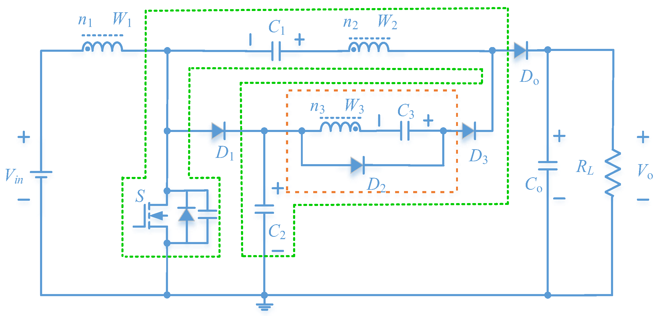
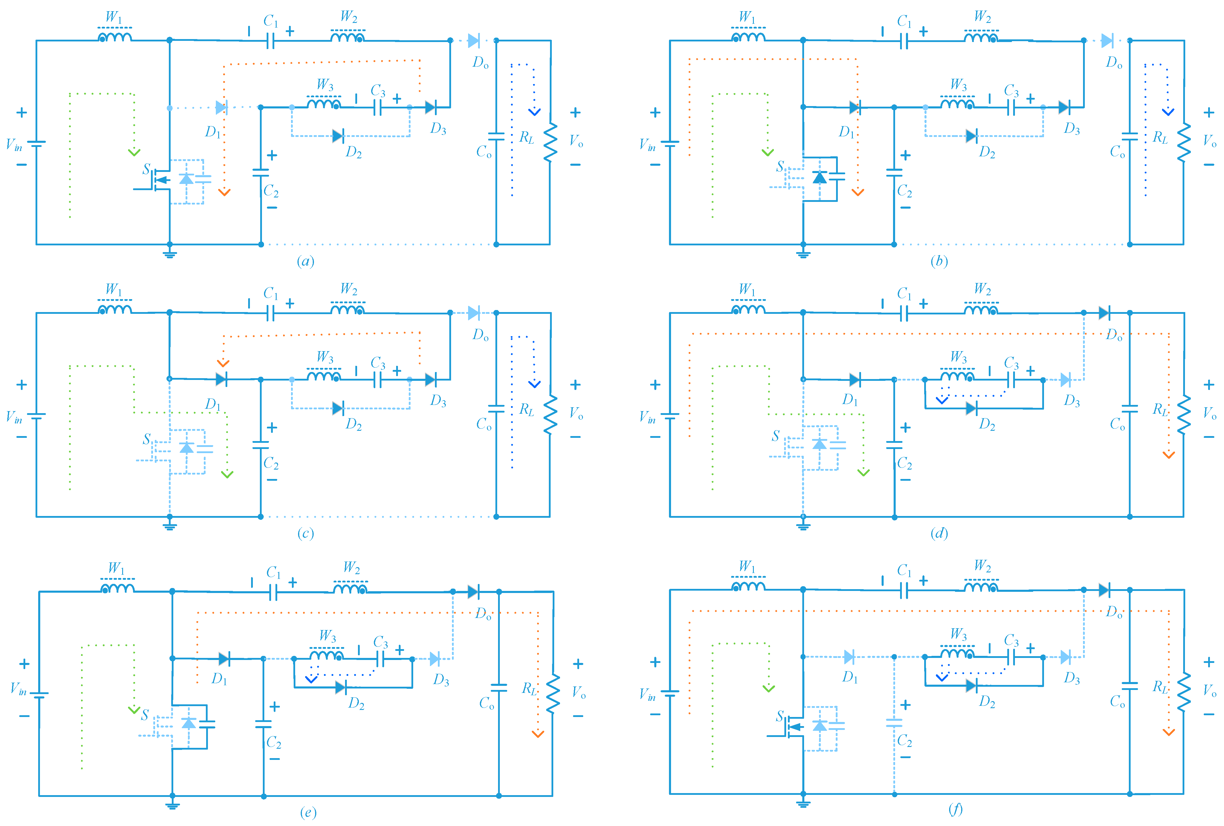
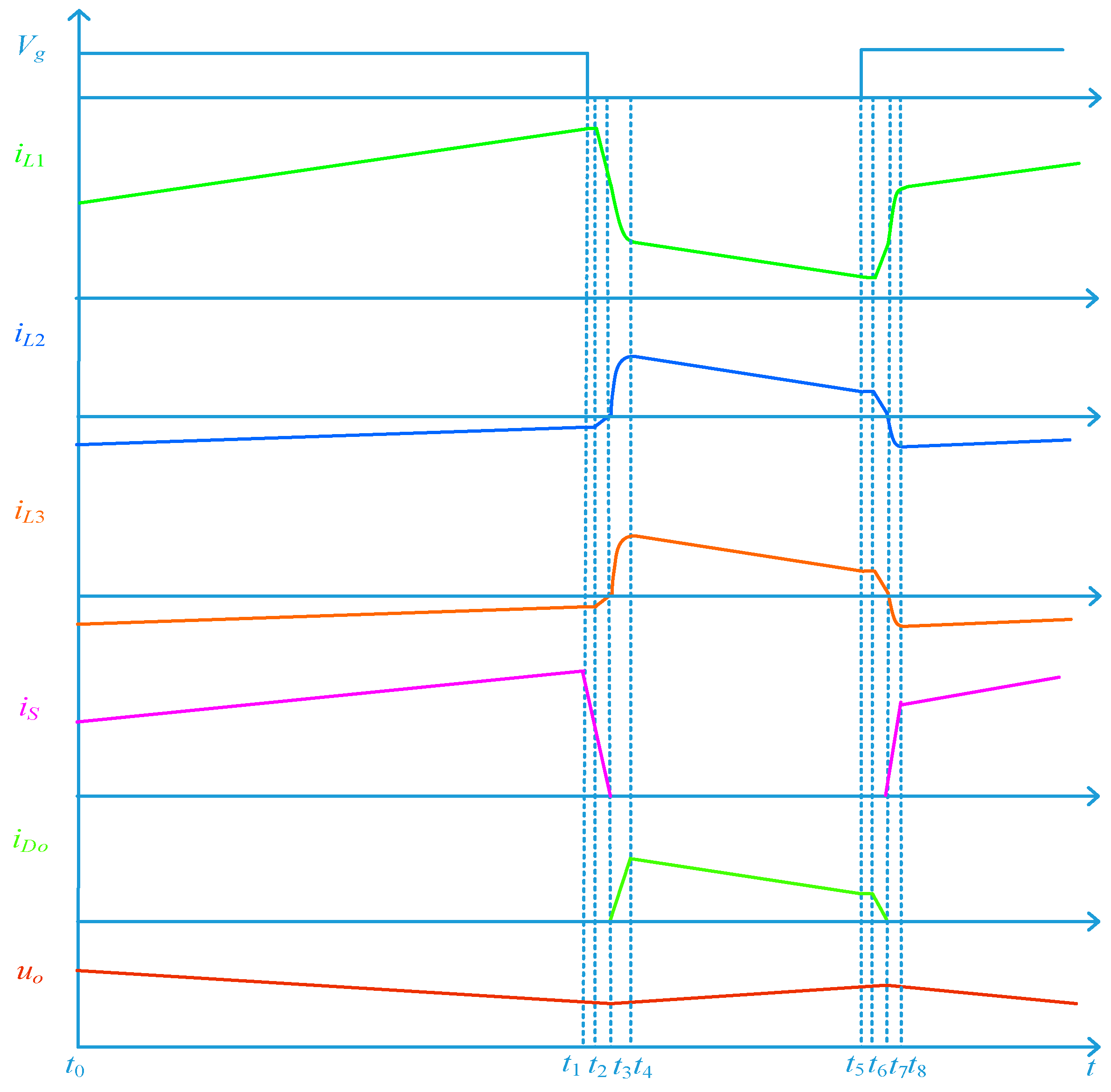
2.1. Operating Modes of the High Step-Up DC/DC Boost Converter

Mode 1 (t0-t1): Switch S and diode D3 are on, while diodes D1, D2 and Do are off. The energy of the load resistor RL originates from the output capacitor Co and the variation of the voltage of the capacitor Co can be neglected (right blue loop in Figure 2a). Energy from the voltage source Vin is stored in the coupled inductor (left green loop). Energy stored in capacitors C2 and C3 is transferred to the clamping capacitor C1 (center orange loop).
The conducting of diode D3 results in the windings W2 and W3 being in series, and the equivalent inductance can be calculated as L23 = L2 + L3 + M23. L2 and L3 are inductances for the windings W2 and W3. M23 is the mutual inductance between the two windings. By applying Kirchhoff’s voltage law to the left green loop and center orange loop in an equivalent circuit in Figure 2a, the following equation set is obtained
      V i n     =       L 1 × d i 1 d t M 1     M 1 , 23 × d i 2 d t M 1 V L 23 M 1 = M 1 , 23 × d i 1 d t M 1     L 23 × d i 2 d t M 1
where L1 is the inductance for the winding W1 and M1,23 is the mutual inductance between winding 1 and the equivalent inductance for windings W2 and W3 in series. VL23M1 is the voltage across the equivalent inductance L23 and can be calculated as the difference between the voltage across the clamping capacitor C1 and the summation of voltages across the capacitors C2 and C3. By solving Equation (2), slopes for the currents in the three windings can be achieved
d i 1 d t M 1 = V i n × L 23 V L 23 M 1 × M 1 , 23 L 1 × L 23 M 1 , 23 2   d i 2 d t M 1 =   V i n × M 1 , 23 V L 23 M 1 × L 1 L 1 × L 23 M 1 , 23 2
Mode 2 (t1-t2): Switch S is turning off and diode D1 is turning on. The energy of the load resistor RL is provided by capacitor Co. Energies stored in the leakage inductances for the three windings of the coupled inductor are transferred to the three clamping capacitors. High frequency oscillations and ripples are formed across these capacitors. The lasting time of this mode is very short and the currents for the three windings can be regarded as constant. This mode is usually neglected in most studies.
Mode 3 (t2-t3): The origin of the energy of the load RL is the output capacitor Co, which is the same as those in the two previous modes. The polarities of the three windings are reversed and two novel loops are formed (green loop and orange loop in Figure 2c). The voltage across the winding W1 in this mode Vdis can be calculated using amp-second balance.
V d i s = V i n × D 1 D = V i n × D D
where D is the duty ratio and equal to the ratio of the conduction time to the period. Similar to the analysis of Mode 1, Kirchhoff’s voltage law is applied to the left green loop and center orange loop in an equivalent circuit. Decreasing slopes for the currents in the three windings of the coupled inductor can be achieved
d i 1 d t M 3 = V d i s × L 23 V L 23 M 3 × M 1 , 23 L 1 × L 23 M 1 , 23 2   d i 2 d t M 3 = V d i s × M 1 , 23 + V L 23 M 3 × L 1 L 1 × L 23 M 1 , 23 2
where VL23M3 is the difference between the voltages across the capacitors C1 and C3, VL23M3 = VC1 − VC3. In the ending time of Mode 3, the currents in windings W2 and W3 of the coupled inductor are decreased to zero.
Mode 4 (t3-t4): Switch S and diode D3 are off. Diode D1 is on. From time t3, diodes D2 and Do enter a conducting state, and energy dissipated by the load RL mainly originates from the coupled inductor. In the end of this mode t4, the current in winding W1 is equal to the summation of the currents in windings W2 and W3. The conduction of the diodes D2 and Do can be considered resonant processes determined by the junction capacitances of diodes and the leakage inductances of the windings W2 and W3. These processes will be studied intensively.
In the loop formed by winding W3, diode D2 and a clamping capacitor C3 (labeled with a blue dashed line in Figure 2d), the junction capacitance for the diode D2, CJD2, is significantly smaller than the capacitance of the clamping capacitor C3, and the leakage inductance of the winding W3, L3Lk, is also smaller than the conductance of the winding. The current in the loop (the same current following through winding W3) increases with the resonance process formed by the junction capacitance and the leakage inductance. The lasting time for this mode is one quarter of the period of the resonance, which can be calculated as T R e s 1 M 3 = 2 π × L 3 L k × C J D 2 .
Similarly, in the increasing process for the current following through the winding W3 determined by the loop formed by diodes Do and D1, clamping capacitors C1 and C2 and winding W2 are in a resonance process. The period for the resonance is T R e s 2 M 3 = 2 π × L 2 L k × C J D o . CJD0 and L2Lk are the junction capacitor of diode Do and the leakage inductance of the winding W2. This means that the currents in windings W2 and W3 reach their positive maximum values at the same time as t4.
Neglecting the difference in the impedances of the above two loops, the currents in the windings of W2 and W3 in the end of this mode t4 are
i 2 ( t 4 ) = i 3 ( t 4 ) = 1 2 i 1 ( t 4 )
Mode 5 (t4-t5): The equivalent circuit for this mode is the same as that of the Mode 4 (Figure 2d) and no change of the switching states for the power devices has occurred. Energy stored in the coupled inductor and clamping inductor C1 are transferred to the output capacitor Co and load RL in this mode, and the current in winding W1 is the same as the summation of the currents of windings W2 and W3. Windings W2 and W3 are in parallel, and the equivalent inductance can be calculated as
L 23 = L 2 × L 3 M 23 2 L 2 + L 3 2 × M 23
where M23 is the mutual inductance between windings W2 and W3. In most prepared coupled inductors with the same turn number for the two windings W2 and W3, L 23 is equal to the inductance of winding W2 or winding W3. The inductance of winding W1 is in series with the equivalent inductance L 23 . The equivalent inductance of the three windings of the coupled inductance is L e q M 5 = L 1 + L 23 + M 1 , 23 . M 1 , 23 is the mutual inductance between the inductance of winding W1 and equivalent inductance L 23 . The slope for the current in winding W1 is
d i 1 d t M 5 = V o V i n V C 1 L e q M 5
The summation of the slopes of the currents in windings W2 and W3 is the same as that of winding W1. The ratio of the slopes of the windings W2 and W3 is determined by the impedances of two loops formed by the winding W3, diode D2 and clamping capacitor C3 (labeled with a dashed blue line), and winding W2, clamping capacitors C1 and C2, diodes Do and D1, output capacitor Co and load RL (in the orange dashed line) (in Figure 2d), respectively. In the following analysis, this difference is neglected.
Mode 6 (t5-t6): Switch S is in the transient process of turning on and diode D1 is in the transient process of turning off. The equivalent circuit for the converter is presented in Figure 2e. High frequency ripples originating from the oscillations between the leakage inductances of the three windings in the coupled inductor and the junction capacitors of the power devices are formed. Due to the short time of this mode, it can be neglected, which is similar to Mode 2.
Mode 7 (t6-t7): Switch S and diodes Do and D2 are on. Diodes D1 and D3 are off. Three loops are formed in this mode (Figure 2f). Comparing with Mode 5, the polarities of voltages across the three windings of the coupled inductor are reversed. From the left loop in Figure 2f (in green), it can be seen that the voltage across the winding W1 is Vin. The voltages across the windings W2 and W3 are Vo  VC1 and VC3, respectively. Slopes for the currents in the three windings of the coupled inductor can be calculated with the following equation set
        V i n = L 1 × d i 1 d t M 7 M 12 × d i 2 d t M 7 M 13 × d i 3 d t M 7 V o V C 1 = M 21 × d i 1 d t M 7 L 2 × d i 2 d t M 7 + M 23 × d i 3 d t M 7         V C 3 = M 31 × d i 1 d t M 7 + M 32 × d i 2 d t M 7 L 3 × d i 3 d t M 7
where Mij (1 ≤ i,j ≤ 3 and ij) is the mutual inductance between winding i and winding j and Mij = Mji. The achieved slopes for the currents in the three windings of the coupled inductor are listed in Equation (9).
d i 1 d t M 7 = V i n ( L 2 L 3 M 23 2 ) ( V o V C 1 ) ( L 3 M 12 + M 12 M 23 ) V C 3 ( L 2 M 13 + M 12 M 23 ) L 1 L 2 L 3 L 1 M 23 2 M 13 2 L 2 M 12 2 L 3 2 M 12 M 13 M 23 d i 2 d t M 7 = V i n ( L 3 M 12 + M 13 M 23 ) ( V o V C 1 ) ( L 1 L 3 M 13 2 ) V C 3 ( M 12 M 13 + L 1 M 23 ) L 1 L 2 L 3 L 1 M 23 2 M 13 2 L 2 M 12 2 L 3 2 M 12 M 13 M 23 d i 3 d t M 7 = V i n ( L 2 M 13 + M 12 M 23 ) ( V o V C 1 ) ( L 1 M 23 + M 12 M 13 ) V C 3 ( L 1 L 2 + M 12 2 ) L 1 L 2 L 3 L 1 M 23 2 M 13 2 L 2 M 12 2 L 3 2 M 12 M 13 M 23
Mode 8 (t7-t8): Switch S is on, and diodes D1, D2 and Do are off. The currents in windings W2 and W3 are decreased to negative maximal values in resonance transient processes, which are similar to the resonances in Mode 4. The lasting time for this mode can be calculated as one quarter of the period determined by the junction capacitance of diode D2. The equivalent inductance L23 formed by windings W2 and W3 in series. The period of the resonance can be calculated with Equation (10).
T R e s 3 M 8 = 2 π × L 23 × C J D 3
where CJD3 is the junction capacitor for diode D3. L23 is the equivalent inductance with a value of L23 = L2 + L3 + M23, which is the same as that of Mode 1. In the ending time of this mode t8, the operating of the converter enters Mode 1 and the complete cycle is realized.

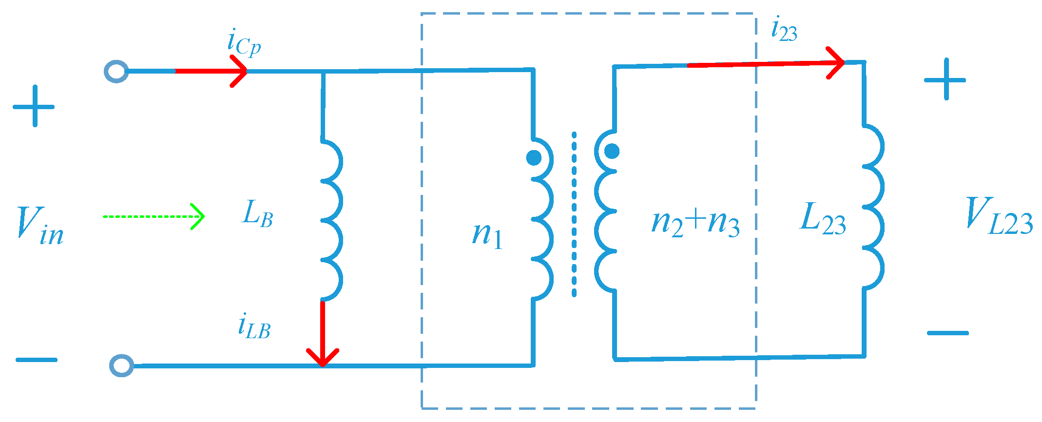
2.2. Simplified Models for Currents in the Three Windings of the Coupled Inductor

Current in the three windings of the coupled inductor can be divided into two parts, the alternating current (AC) component and direct current (DC) component. As energies in the coupled inductor are stored in Mode 1 and released in Mode 5, other transient modes are neglected. The simplified waveforms for these currents are presented in Figure 4. The AC components of these currents can be calculated with the slopes obtained in the previous analysis of the operating modes. However, the DC components for these currents are still unclear, and the design requirements of the inductor can not be satisfied.
The DC components for currents in the three windings are calculated first. The charge balance of a capacitor in DC/DC converters means that the quantity of charge injected into the capacitor is equal to that released in a switching period, which is another form of amp-second balance [35]. By applying a charge balance to the capacitor Co, the capacitor can be neglected in calculations of the quantity of charges following through the load RL. The charges through the load RL in a switching period (presented with a green dashed line in the bottom of Figure 4) are
Q o = I o × T s = V o R L × T s
where Vo is the output of the high step-up converter, Io is the output current of the converter and Ts is the switching period. The charges through the RL are the same as those following through diode Do (orange dashed line in Figure 4), QDo = Qo. The current of the diode Do in conducting state IDo is
I D o = Q D o ( 1 D ) × T s = I o 1 D
The charges following through winding W2 in Mode 5 are the same as those following through diode Do. Moreover, the quantities of the charges through winding W2 in Mode 1 and Mode 5 are the same. These relationships in the charges are also suitable for analysis on winding W3. Models for estimating the DC currents in the windings W2 and W3 are listed as follows
I L 23 o n = I o D I L 23 o f f =     I D o
where IL23on and IL23off are the DC components for currents in windings W2 and W3 in Modes 1 and 5, respectively.
As charges following through winding W1 in Mode 5 QL1off are the summation of those in windings W2 and W3, this current can be calculated with Equation (18). The power balance means that the input power of a DC/DC converter is equal to the output power in a switching cycle. The DC current in winding W1 in a switching cycle is M × Io. M is the voltage gain of the converter. The charges through winding W1 in Mode 1 are (M − 2) × Io. The DC component of the current in winding W1 in Mode 1 can be calculated.
I L 1 o n = I L 1 I L 1 o f f = M 2 D × I o     I L 1 o f f = 2 × I D o = 2 1 D × I o
Ripples in the currents of the three windings of the coupled inductor will be investigated in the following section. Ripples in the three currents (in Figure 4) are formed by the differences in the DC components and AC components in Mode 1 and 5. Differences in the DC components of the three windings can achieved
i L 1 r i p D C =     I L 1 o n I L 1 o f f   = ( M 2 D 2 1 D ) × i o i L 23 r i p D C = I L 23 o n I L 23 o f f = ( 1 D + 1 1 D ) × i o
Although the AC components of the currents in the three windings of the coupled inductor can be calculated with their slopes in Modes 1 and 5 (Equations (2) and (7)), these calculations are complicated, and the characteristics of the coupled inductor are not included. Most coupled inductors are prepared with magnetic cores, and the coupled coefficients between different windings in the inductor are close to 1. A simplified model of the coupled inductor in Mode 1 is presented in Figure 5.
The three-winding coupled inductor operating in Mode 1 is modeled with a two-terminal network (from the green arrow in the left of Figure 5). LB is the boost inductance and L23 is the inductance of the windings W2 and W3 in series. Inductance L23 is coupled to the boost inductance with an ideal transformer with a turn ratio of n1:(n2 + n3). Inductances for the isolated winding W1 and the two windings W2 and W3 in series are L1 and L23, respectively. The relationship between the two inductances is
L 23 = L 1 × ( n 2 + n 3 n 1 ) 2
L 23 is the inductance of L23 transformed to the primary side of the ideal transformer with a value of L1, which is the same as that of winding W1. This is attributed to the tight coupling between the three windings and the same magnetic flux in these windings.
From analysis of the operating modes of the coupled inductor in an entire switching period, it can be confirmed that the variations of the currents following through windings W1 and W2 are zero, and the energy is mainly stored in winding W1. The slope for the current following in the two-terminal network is diCp/dt = Vin/L1. This current slope is divided into two equal parts, the slope for the current in the boost inductance and the slope for the current in the inductance L 23 . The same inductance leads to the equal current slope with a value of Vin/(2 × L1).
The slope for the current in the boost inductance means that its equivalent value is two times the inductance of winding W1. This is beneficial to depress the AC component in the ripple in the current of winding W1. Similarly, the current slope for the equivalent inductance L23 can be achieved and presented in Equation (17).
      d i 1 d t M 1 = V i n 2 × L 1 d i 23 d t M 1 = V i n 2 × L 1 × n 1 n 2 + n 3
The slopes of the three windings in Mode 1 can be estimated with the inductance of winding W1 and turn ratios of the three windings, which can reduce the difficulty of designing the coupled inductor significantly.
Energies stored in the coupled inductor are transferred to the load of the converter in Mode 5. Windings W2 and W3 are in parallel, and their equivalent inductor is in series with winding W1. To balance the currents in windings W2 and W3, the two windings have the same turn numbers. The equivalent inductance of the three windings of the coupled inductor can be estimated with the following equation
L c p M 5 = ( n 1 + n 2 n 1 ) 2 × L 1
Voltage across the equivalent inductance can be calculated as
V L c p M 5 = ( n 1 + n 2 n 1 ) × V d i s
The slope for current in winding W1 in Mode 5 is
    d i 1 d t M 5 = V d i s L 1 × n 1 n 1 + n 2 d i 23 d t M 5 = V d i s 2 × L 1 × n 1 n 1 + n 2
The slopes for currents in windings W2 and W3 are half of the slope of current in winding W1.
Finally, a model of the current in winding W1 is established
i 1 ( t ) =             M 2 D × i o + V i n 2 × L 1 × ( t D × T s 2 )                                   0 < t D × T s 2 D × i o V d i s L 1 × n 1 n 1 + n 2 × [ t ( 2 D + D ) × T s 2 ]     D × T s < t T s
Similarly, models of the currents in windings W2 and W3 are obtained
i 23 ( t ) =       1 D × i o + V i n 2 × L 1 × n 1 n 2 + n 3 × ( t D × T s 2 )                           0 < t D × T s 1 D × i o V d i s 2 × L 1 × n 1 n 1 + n 2 × [ t ( 2 D + D ) × T s 2 ]       D × T s < t T s
With the established models, currents in the three windings of the coupled inductor can be estimated, with the boost inductance determined by winding W1 and the turn numbers of the three windings, which can significantly reduce the difficulty of designing the coupled inductor. High-frequency parasitic effects, such as the leakage inductances and parasitic capacitors in the three windings of the coupled inductor, are neglected in the current models. The errors of the models cannot be neglected in the analysis of the converter operating at high frequencies.

3. Design on the Three-Winding Coupled Inductor

In the previous analyses, accurate and simplified models of the currents in the three windings of the coupled inductor were established. These are foundation of design of the coupled inductor. A novel method of designing the inductor will be proposed in the following section. The method is divided into four parts: determining the required conductance for winding W1 in the coupled inductor, selecting a magnetic core with the product areas (AP) method, determining the windings’ arrangement and evaluating the loss of the coupled inductor.

3.1. Determining the Required Inductance of Winding W1 in the Coupled Inductor

Ripples in the current following through winding W1 (in Equation (23)) can be divided into two parts: the difference in the DC components for currents in Modes 1 and 5 and the AC component determined by the boost inductance.
i L 1 r i p = ( M 2 D 2 1 D ) × I o + V i n L 1 × D × T s 2 + V d i s L 1 × n 1 n 1 + n 2 × D × T s 2                 = ( M 2 D 2 1 D ) × I o D i f f e r e n c e   i n   D C   C u r r e n t s + V i n × D × T s L B × ( 1 + n 1 n 1 + n 2 ) A C   c o m p n e n t s
From Equation (23), it can be found that the DC components of the current in winding W1 play an important role in the formation of its ripple, and this ripple can be depressed by properly increasing the duty of the converter. More important, a high duty is also required by the high voltage gain. The voltage gain of the high step-up converter in Figure 1 can be calculated with the following equation
M = N 1 + N 2 + 2 1 D
where N1 and N2 are the turn ratios for windings W2 and W3 to winding W1. More details of calculating the voltage gain of the high step-up converter can be found in the Appendix A. To decrease the ripple in the current of winding W1 and improve the voltage gain of the converter, the duty is chosen as 0.60. With a parallel coiling structure for windings W2 and W3, the leakage flux can be depressed significantly. This means that the two windings have the same turn numbers and turn ratios N1 and N2 have the same value. Using Equation (24), the turn ratios N1 and N2 can be estimated at a value of 1.00. Finally, the achieved turn ratio for the three windings of the coupled inductor is 1:1:1, which is also found in refs. [19,20,24,27,28].
Furthermore, the required inductance for winding W1 of the coupled inductor can be achieved, which is half of the boost inductance
L 1 = V i n × D × T 2 × ( i L 1 r i p i L 1 r i p D C ) × ( 1 + n 1 n 1 + n 2 )
where iL1rip is the total ripple of the current in winding W1 and iL1ripDC is the difference between the DC components of the currents in Modes 1 and 5 (right item in Equation (22)).
The parameters of the high step-up DC/DC converter are listed in Table 1. They are the foundation of the design of the three-winding coupled inductor. The difference in the DC components of the ripple of the current in winding W1 is 7.88 A, and the AC component in the current is 2.12 A. Furthermore, the required inductance for winding W1 can be obtained with Equation (25). The achieved result is 109.67 µH.

3.2. Product Areas (AP) Method for Magnetic Core Selecting

Selecting an appropriate core is an important work in the design of the magnetic elements. The product areas (AP) method has been widely used in designs of traditional transformers and inductors. However, no report on the AP method being used to design a multi-winding coupled inductor has been found. In Mode 1 (Figure 2a), the voltage is applied to winding W1 and the following relation is formed
V i n = L 1 × d i 1 / d t   = n 1 × d ϕ / d t   = n 1 × Δ B × A e D × T s
where n1 is the turn number for winding W1. ΔB is the variation of the magnetic induction intensity. Ae is the effective area of the magnetic core.
Assuming the converter operates in the linear region of the hysteresis loop, the following relationship can be established
Δ B B m = Δ I L 1 I L 1
where Bm is the peak magnetic induction intensity. ΔIL1 is the ripple of the current in winding W1 and IL1 is the peak value for the current. By defining kIL1 = ΔIL1/IL1, the variation of the magnetic induction intensity can be calculated as ΔB = Bm × kIL1. The desired effective area of the magnetic core Ae is
A e = V i n × D × T n 1 × k I L 1 × B m
The winding area of the magnetic core is determined by the root-mean-square (RMS) values of the currents in the three windings
A w = n 1 × I L 1 r m s + n 2 × I L 2 r m s + n 3 × I L 3 r m s j × k w
where ILirms is the RMS value of the current in the winding i. j is the current density of the three windings. kw is the utilization factor of the winding window.
The areas product formula for selecting the magnetic core of the coupled inductor can be established
A P = A e × A w = D × V i n × 1 i 3 n i n 1 × I L i r m s f × k I L 1 × B m × j × k w
Using the simplified models of currents in the three windings of the coupled inductor in Equations (21) and (22), RMS values for these currents are calculated and listed in Table 2. Furthermore, the peak magnetic induction intensity, current density and utilization factor of the winding window are set as 0.36 T, 7.50 A/mm2 and 0.60, respectively. The obtained AP value for the three-winding coupled inductor is 28,262.60 mm4. The corresponding value for the ETD39 core manufactured by the Ferroxcube company using the material 3C95 is 29,287.50 mm4.

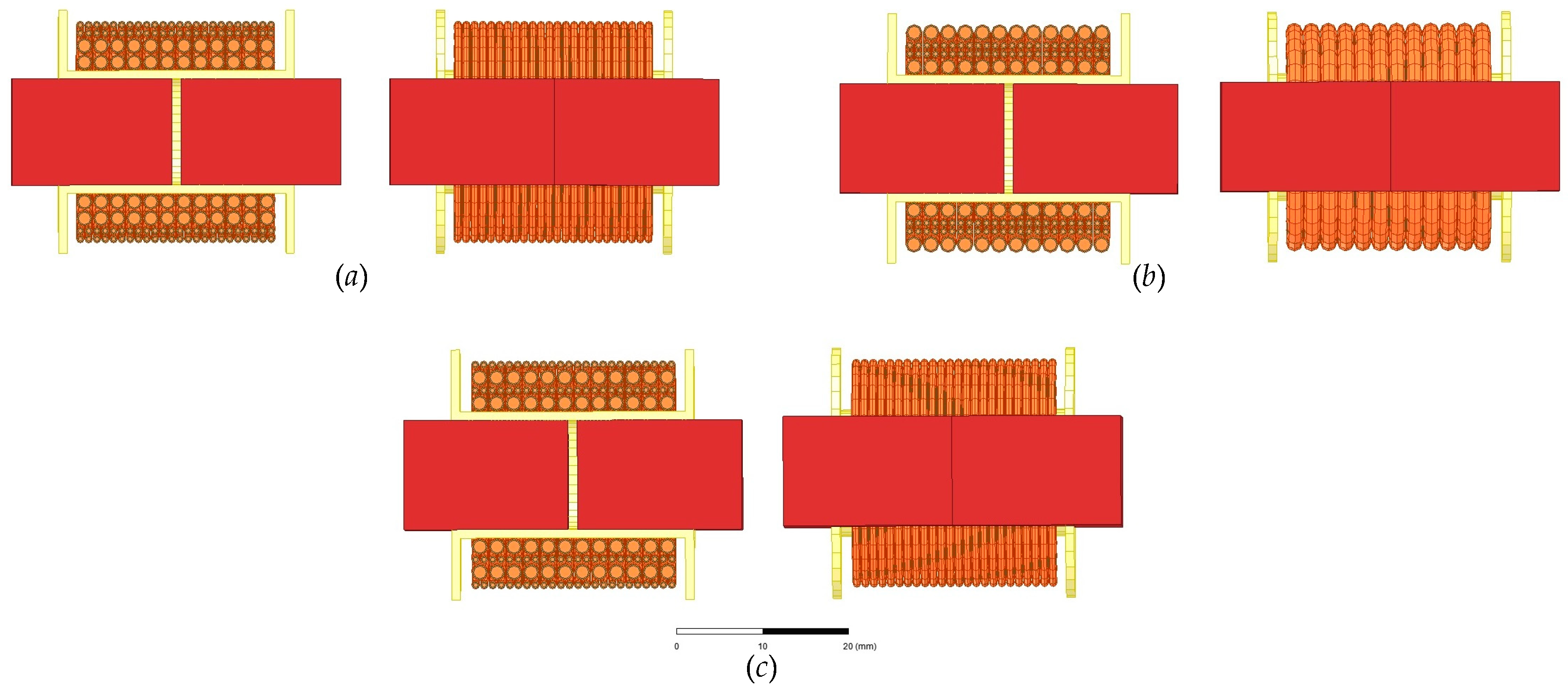
3.3. Winding Arrangement for the Coupled Inductor

With the selected magnetic core, the turn number for the winding W1 can be estimated using Equation (34). Furthermore, the turn numbers for the other two windings are calculated with the turn ratios of N1 and N2 calculated using Equation (24).
n 1 = V i n × D × T s k I L 1 × B m × A e
To avoid the core entering a saturation state, the variation of the magnetic induction intensity is set as 0.25 T and smaller than the peak magnetic induction intensity in Equation (28). The effective area of the ETD 39 core is 125.0 mm2. The turn number for winding W1 in Equation (31) is 24.25. In preparing the coupled inductor, the three windings are coiled with the same turns number of 24.0.
The boost inductance L1 based on the achieved turn number and magnetic core without an air gap can be estimated as
L 1 = n 1 2 × u × A e l e
where u and le are the permeability and effective length of the magnetic circuit of the magnetic core. The achieved inductance is 2.12 mH. An air gap must be implemented in the center leg of the magnetic core. The length of the gap δ can be calculated as
L 1 = n 1 2 1 / A L + δ / ( μ 0 × A × δ )
where u0 is the permeability of the vacuum and A is the area of center leg of the core. AL can be calculated as AL = u × Ae/le. The obtained length of the air gap is about 1.00 mm.
Selecting the appropriate copper wires to coil windings in the coupled inductor is another important work. To reduce losses caused by eddy effects, Litz wires are usually used to prepare transformers and inductors. The required effective sectional areas of the Litz wires for coiling the three windings are 1.44 mm2 and 0.27 mm2, respectively. Considering the actual dimensions of the ETD39 core former, round Litz wire of 200 strands/AWG40 with an effective sectional area of 1.54 mm2 and diameter of 1.90 mm is adopted to coil winding W1. Windings W2 and W3 are coiled with Litz wire of 50 strands/AWG40. The diameter of the Litz wire and its effective sectional area are 1.00 mm and 0.38 mm2.
The winding arrangement has significant impacts on the performance of the coupled inductor. A concentric winding structure is used. Three windings of the coupled inductor are coiled on the central leg of the core in a sequence of W1-W2-W3 (presented in Figure 6a). The two inner layers are winding W1 and the two outer layers are windings W2 and W3. No interleaving is formed between winding W1 and the other two windings. Weak coupling may lead to a large leakage inductance. By dividing winding W1 into two parts, two different winding arrangements with a strong coupling are formed. Corresponding coiling sequences for the four layers of the windings are 1/2W1-W2-W3-1/2W1 and 1/2W1-W2-1/2W1-W3 (in Figure 6b,c).
To investigate the impact of winding arrangement on the performance on the coupled inductor, a finite element analysis (FEA) on the coupled inductors was implemented with Maxwell package. In simulations, the eddy current was selected as a solution type to calculate the inductances and magnetic induction intensity vectors. In the meshing processes, the maximum lengths for the elements in the core and the windings were set as 1.0 mm and 0.5 mm, respectively. The convergence criterion was that the difference for the energies in two adjacent calculations had to be smaller than 0.5% of the total energy. The achieved inductances for winding W1 and the leakage inductances with different winding arrangements are listed in Table 3. From Table 3, it can be found that the difference in the inductances of windings W1 with different winding arrangements can be neglected. The inductance is determined by the turn number of winding W1 and the length of the air gap in the center leg of the magnetic core. Interleaving between the three windings of the coupled inductor can suppress magnetic flux leakage and decrease the leakage inductance. The minimum leakage inductance for the coupled inductor is 2.91 µH in a winding sequence of 1/2W1-W2-1/2W1-W3, which is about 55.2% of the leakage inductance with a winding sequence of W1-W2-W3.
Comparing the current density in the three windings of the coupled inductor with different coiling sequences (in Figure 7), it can be found that the interleaving between adjacent layers of different windings can improve the uniformity of current in the coupled inductor. The highest current density in the coupled inductor with a winding sequence of W1-W2-W3 is located at the interface between winding W1 and winding W2, which originates from the proximity effect in the two windings (in bottom of Figure 7a). This is consistent with the highest magnetic induction intensity for the magnetic leakage (in the top of Figure 7a). The uniformity of the current densities of the coupled inductor with the coiling sequences 1/2W1-W2-W3-1/2W1 and 1/2W1-W2-1/2W1-W3 is improved significantly (at the bottom of Figure 7b,c). The highest magnetic induction intensity of the magnetic leakage in the coupled inductors in the two winding sequences is depressed significantly (at the top of Figure 7b,c). This is consistent with the achieved leakage inductances in Table 3. The coiling sequence of 1/2W1-W2-1/2W1-W3 is an appropriate choice to prepare the coupled inductor.

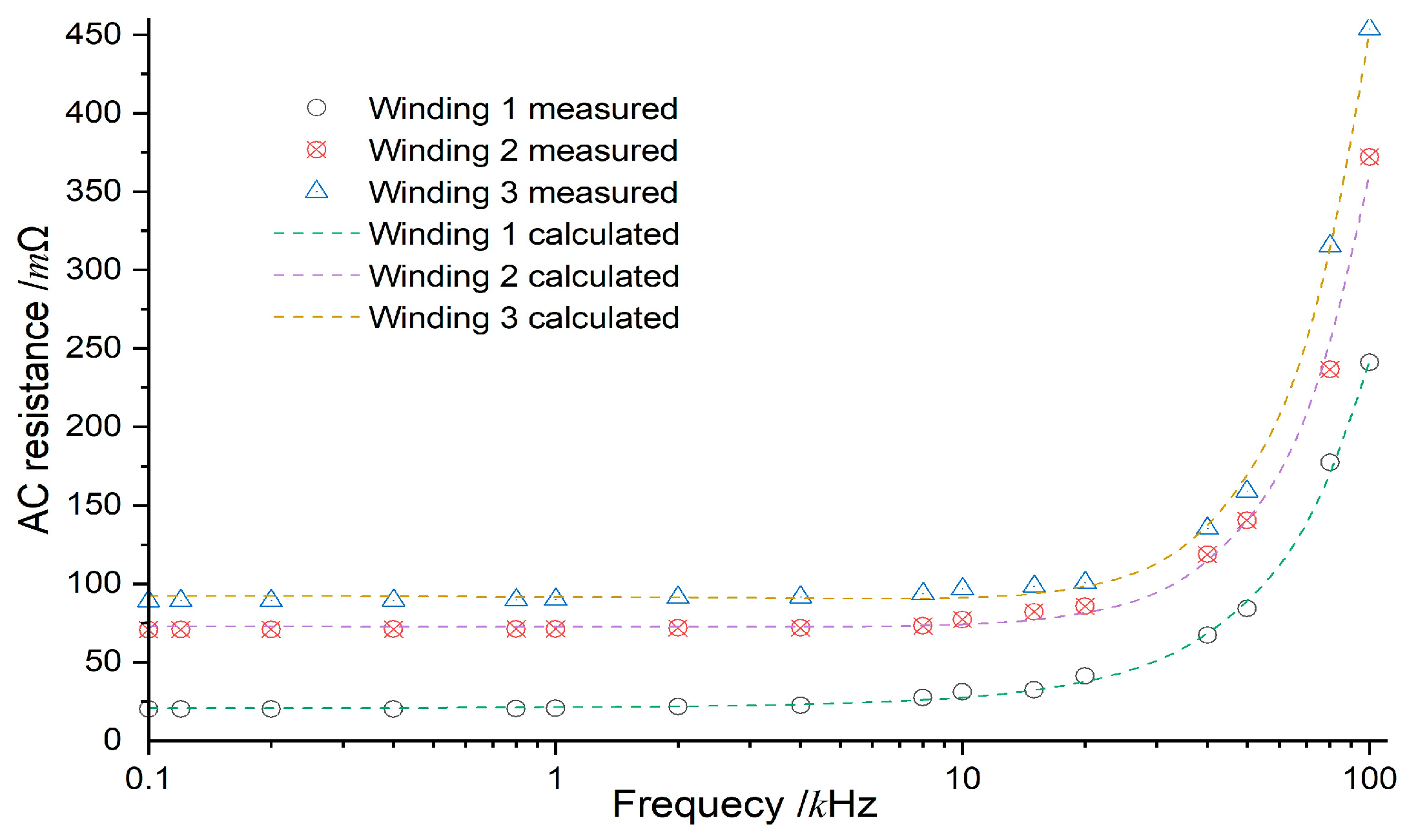
3.4. Loss Evaluation for the Three-Winding Coupled Inductor

Losses in the coupled inductor can be divided into two parts, winding loss Pwind and core loss Pcore. Winding loss mainly originates from the energy dissipations by AC resistances of the windings and can be calculated as
P w i n d = 1 2 1 i 3 R A C W i × I L i r m s 2
where RACWi is the AC resistance of the winding i of the coupled inductor and ILirms is the RMS value of the current in the winding i. The ratio of the AC resistance to the DC resistance of the winding realized with multilayer foils is defined as FR and calculated with the Dowell equation [36].
F R = R s k i n + R p r o x R d c = F R s k i n + F R p r o x = A sinh ( 2 A ) + sin ( 2 A ) cosh ( 2 A ) cos ( 2 A ) + A 2 ( N l 2 1 ) 3 sinh A sin A cosh A + cos A = A φ 1 + A 2 ( N l 2 1 ) 3 φ 2
where FRskin and FRprox are ratios for the resistances caused by the skin effect and the proximity effect. A is the thickness of the foil and Nl is the layer number of the foils. For windings realized with Litz wire, effective layer number Nll for the winding is modeled by the strand number k and Nl is the real layer number of the winding [37]
N l l = k N l
Considering the skin depth, the effective thickness for the strand layers in Litz wire Aef is modeled
A e f = ( π 4 ) 0.75 η d s t r δ η = d p = k d s t r p   δ = 1 π f μ 0 σ
where η is the equivalent porosity factor for the Litz wire windings, p is the sum of the diameter and the distance between two adjacent wires, δ is the skin depth, μ0 is the free space permeability, f is the operating frequency, and σ is the conductivity. With the effective layer number Nll and effective thickness Aef (in Equations (36) and (37)) for Litz wire, the AC resistances of the three windings in the coupled inductor with winding sequences of 1/2W1-W2-1/2W1-W3 are calculated and presented in Figure 8 with dashed lines.
The Steinmetz equation is widely used in calculating core loss, which is listed as follows [38].
P c o r e = K × f α × Δ B β × C T
where K, α, and β are parameters related to the core material, f is the switching frequency of the converter (in kHz) and ΔB is the peak-to-peak magnetic induction intensity (in mT) of the converter with the maximum output power. CT is the temperature coefficient for core loss.
C T = c 0 c 1 t c 2 t 2 + c 3 t 3
In the switching frequency range from 20.0 to 200.0 kHz, K, α and β are 5.46 × 10⁻¹⁴, 1.70 and 2.74, respectively. The parameters for the temperature coefficient CT, c0, c1, c2 and c3 are 1.00, 2.27 × 10⁻³, 1.28 × 10⁻⁵ and 3.88 × 10⁻⁷. The unit of the core loss is mW/cm3.

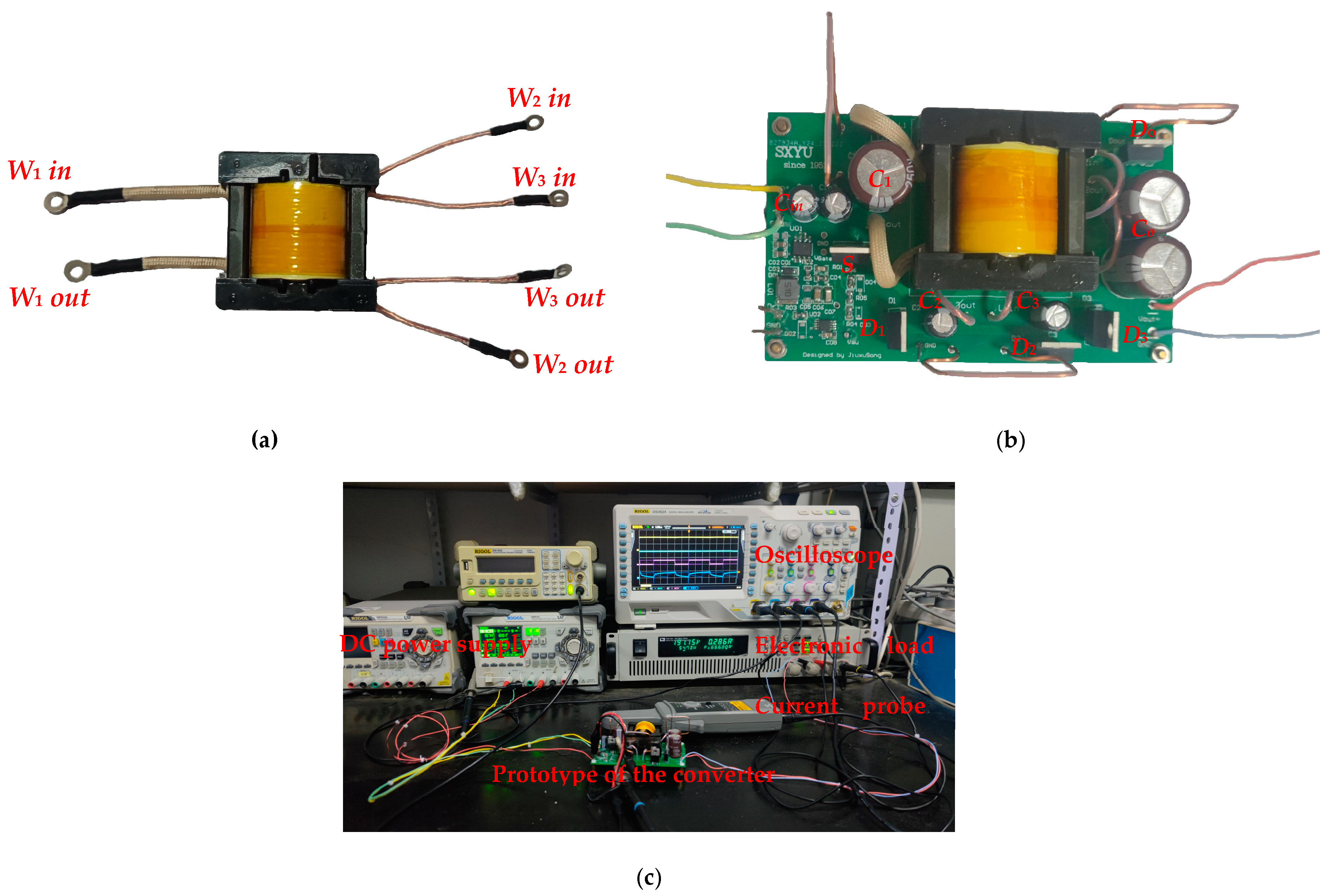
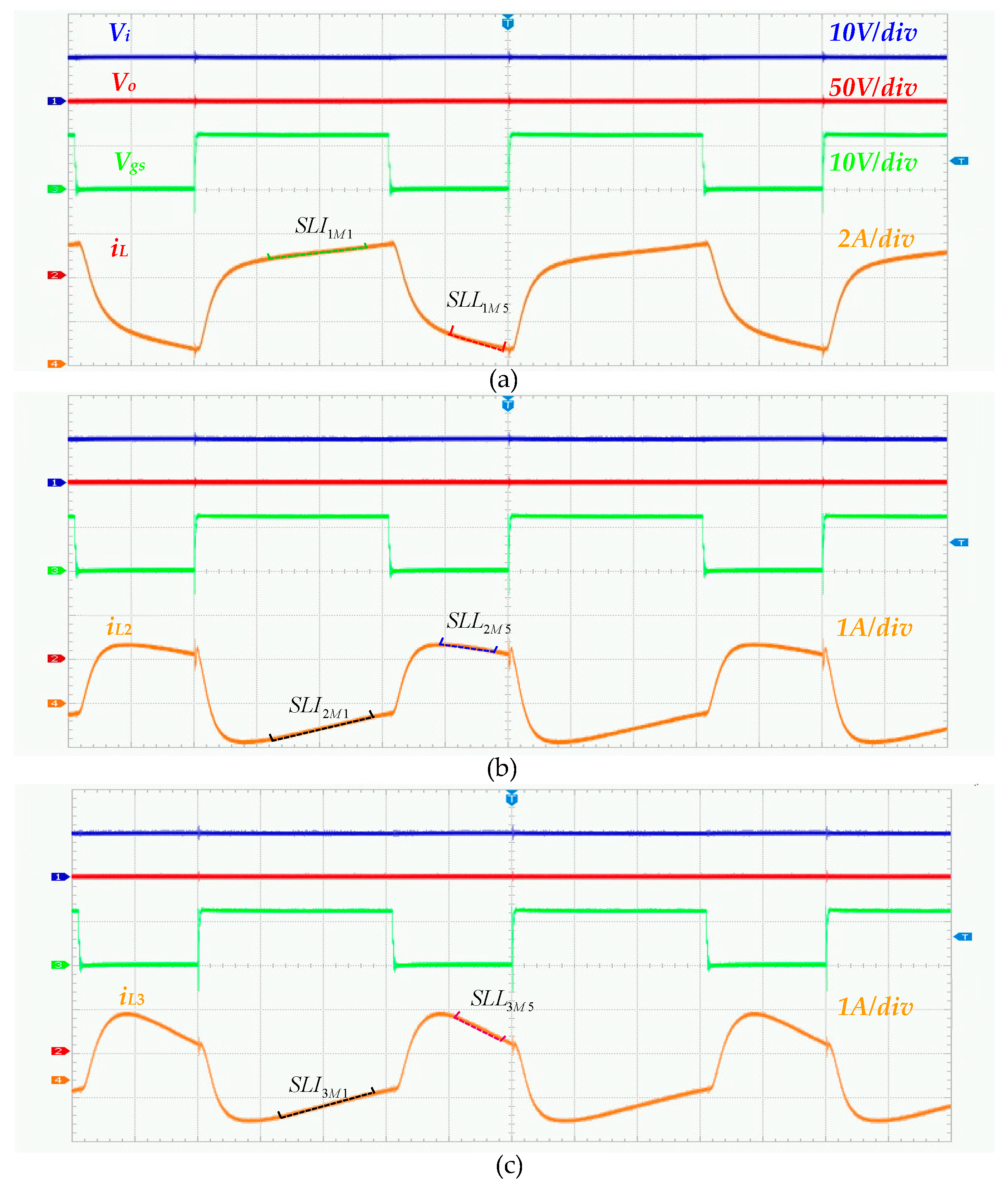
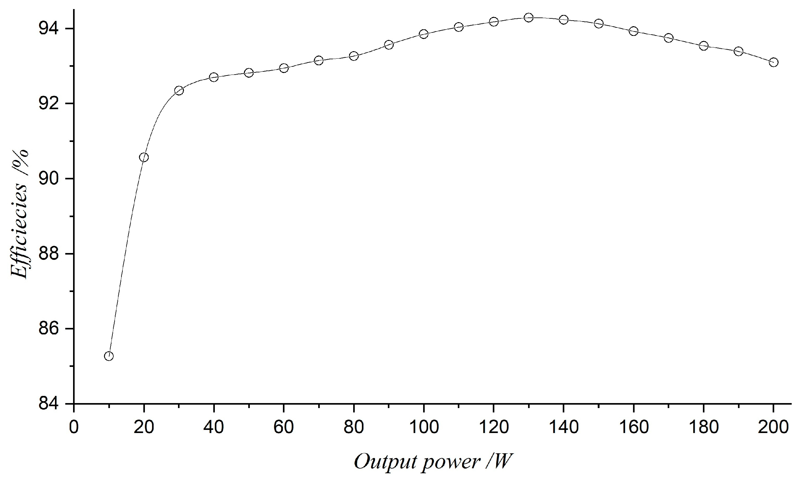
4. Experimental Results

A coupled inductor with coiling sequence of 1/2W1-W2-1/2W1-W3 and air gap length of 1.05 mm in the center leg was prepared and is presented in Figure 9a. The inductor was measured with LCR meter Chroma 11025 (Chroma, Burlington, VT, USA). Under the frequency of 40.0 kHz, the inductance for winding W1 was 105.04 µH, which is consistent with the results of theoretical calculations in a value of 106.65 µH (in Table 3). The error for the inductor was about 1.53% of the measured result. The measured leakage inductance at 40.0 kHz was 3.46 µH and slightly larger than the results of theoretical calculations with a value of 0.58 µH. The difference between the leakage inductance as measured and calculated was about 16.76%. The measured AC resistances at the frequency of 40.0 kHz for the three windings of the coupled inductor were 67.2, 118.7 and 135.5 mΩ (in Figure 8). Due to the resistances of the cables and the kelvin clip of the LCR meter, the measured results were slightly larger than the real resistances. These are consistent with the results of theoretical calculations at values of 68.5, 114.8 and 137.6 mΩ made with the improved Dowell equation for Litz wires.
To compare with other coupled inductors applied in high step-up DC/DC converters, the parameters for the converters and coupled inductors are listed in Table 4. The turn ratios for the coupled inductors in refs. [20,27] were normalized. The switching frequency had a significant impact on the volume of the magnetic element. The switching frequencies for these converters (Table 4) range from 40 kHz to 70 kHz, and the difference can be neglected. Parameter Urcore, which describes the utilization rate of the magnetic core, can be defined as
U r c o r e = P o / V e
where Po is the rated output power of the converter and Ve is the effective volume of the core. A lower Urcore means a lower utilization rate of the magnetic core. The Urcore for the coupled inductor designed in this paper is higher than those of other coupled inductors listed in Table 4. This means that the proposed design method for a coupled inductor is correct.
To further verify the designed coupled inductor, a prototype of the high step-up DC/DC converter was prepared (Figure 9b). Its testing platform is presented in Figure 9c. The coupled inductor is presented in the upper part of the PCB board (Figure 9b). An N channel MOSFET IRFB38N20DPBF from the Infineon company (Neubiberg, Germany) was used as the switch S. To reduce the number of types of components, all diodes D1, D2, D3 and Do were realized with ultra-fast recovery diodes MUR1640CTG manufactured by the Onsemi semiconductor company. The capacitance for the clamping capacitor C1 was 100.0 μF and the capacitance for C2 and C3 were adopted with the same value of 47.0 μF. The capacitances for input filter and output filter capacitors (Cin and Co) were 94.0 Μf and 200.0 μF, respectively. The main components of the converter are listed in Table 5.
The measured waveforms of the high step-up converter with an output power of 80.0 W are presented in Figure 10. The duty of the driving signal of the switching MOSFET S was about 0.61 and the output of the converter was 199.74 V (waveforms in green and wine in Figure 10a). These are consistent with the results of the analysis of the operating modes. The correctness of the operating principle of the converter is preliminarily validated.
The average value of the current in winding W1 (orange waveform in Figure 10a) was about 4.39 A, which is slightly larger than the theoretical value (4.28 A with an efficiency of 93.27%). This difference can be neglected. The RMS value for the measured current in winding W1 was 4.86 A. The theoretical value obtained with the model proposed in this paper is 4.56 A. The measured ripple in the current of winding W1 was 5.31 A. The difference in the DC components of this current between Mode 1 and Mode 5 is 3.96 A. The AC component for the ripple was 1.62 A (in Equation (21)). The ripple in the theoretical calculation is 5.58 A. The difference in the ripples between measured and theoretically calculated is 0.27 A, which is about 5.08% of the measured ripple. The correctness of the current model for the current in winding W1 is verified.
The measured rising slope of the current in winding W1, SLL1M1 (labeled with a green dashed line in the waveform in Figure 10a) is 89.36 mA/µs, and the slope form model established in this paper is 94.88 mA/µs. The difference between the measured and theoretically calculated slope is 6.18 mA/µs (about 6.2% of the measured slope). Similarly, the measured descending slope SLL1M5 (labeled with a dashed red line) and the calculated slope are 149.53 mA/µs and 142.32 mA/µs, respectively. The measured rising slope and falling slopes for the current in winding W1 are consistent with the results from the model in Equation (21). The correctness of the model of the current in winding W1 and the design method for the three-winding coupled inductor are verified.
The waveforms for currents in windings W2 and W3 are presented in the middle and at the bottom of Figure 10b,c). The average values for the two currents are zero, which is consistent with the results of analysis of the operating modes of the high step-up DC/DC converter in Section II. The measured rising slopes of the two currents in Mode 1 (SLL2M1 and SLL3M1, labeled with a black dashed line) are −52.16 mA/µs, which are similar to the established model, which had a value −47.44 mA/µs. The negative sign means that the currents follow out the dotted terminals of the two windings. The measured falling slopes in the two windings are 46.15 mA/µs and 102.13 mA/µs (SLL2M5 and SLL3M5, labeled with blue and purple dashed lines). The summation of the two slopes is equal to the corresponding slope of the current in winding W1 (142.32 mA/µs). This is consistent with the results of operating mode analysis on the Mode 5.
The efficiencies of the prototype of the high step-up converter were tested with loads from 10 W to 200 W. The results are presented in Figure 11. The efficiencies of the high step-up DC/DC converter are higher than 90.0% in the tested range from 20 W to 200 W, in which the appropriately designed coupled inductor plays an important role. The peak efficiency of the converter is about 94.3%. The losses in the coupled inductor with an output of 80.0 W were analyzed in detail. The RMS values for currents in the three windings W1, W2 and W3 of the coupled inductor were 4.86 A, 0.86 A and 0.87 A, respectively. With the measured AC resistances of these windings at 40 kHz, the power loss in the three windings of the coupled inductor in the windings was 1.78 W. With the variation of 100 mT of the magnetic induction intensity in the coupled inductor, the power loss of the magnetic core could be restrained to a value of 1.20 W. The total loss of the converter is about 2.98 W, which is about 55.4% of the total power loss of the converter.

5. Conclusions

Due to the prospects for application in renewable energy generation and DC microgrids, high step-up DC/DC converters have attracted tremendous research interest. By combining a multiple-winding coupled inductor with voltage multipliers, the voltage gain of a boost converter can be improved significantly. However, the lack of a method of designed multi-winding coupled inductors has become an important restriction on the applications of high step-up DC/DC converters.
By analyzing the operating modes of a boost converter combined with a three-winding coupled inductor and double voltage multipliers, accurate models of currents in the three windings of the coupled inductor are established. Furthermore, simplified models of these currents are proposed. The relationship between the ripple in the input current of the coupled inductor (Winding W1) and the boost inductance is established.
A method of designing a coupled inductor is proposed, in which a method of estimating the required inductance for winding W1 of the coupled inductor, an improved product areas (AP) method to select a magnetic core, the influence of the windings’ arrangement and a loss evaluation for the coupled inductor are investigated in detail.
A prototype of the 200 W DC/DC converter with an input of 20 V and an output of 200 V was prepared and testified. The results indicate that the measured waveforms are consistent with the established models of currents in a coupled inductor. The efficiency of the converter is higher than 90.0% in the testing range for outputs from 20 W to 200 W. The correctness of the method of designing a multi-winding coupled inductor has been verified. The proposed method can be applied to the design of multi-winding coupled inductors, especially inductors applied in high step-up DC/DC converters operating as interfaces between renewable sources and DC microgrids.

Author Contributions

Conceptualization, J.S.; methodology, J.S., J.W., S.D. and B.J.; software, J.W. and S.D.; validation, J.S., J.W. and S.D.; formal analysis, J.S., J.W., Y.Q., S.D. and B.J.; investigation, J.S. and B.J.; resources, J.S., Y.Q. and B.J.; data curation, J.S., J.W., Y.Q., S.D. and B.J.; writing—original draft preparation, J.W. and S.D.; writing—review and editing, J.S., J.W., Y.Q., S.D. and B.J.; visualization, J.S., J.W. and S.D.; funding acquisition, J.S. and B.J. All authors have read and agreed to the published version of the manuscript.

Funding

This work was supported by the Marie Skłodowska-Curie Actions (MSCA) under the European Union’s Horizon 2020 Research and Innovation Staff Exchange (RISE) under Grant 872001. This work was supported Key Research and Development Program of Shaanxi Province under Grant No. 2022GY-135.

Data Availability Statement

The data that support the findings of this study are available from the authors, Jiuxu Song and Bing Ji, upon reasonable request.

Conflicts of Interest

Author Yuanzhong Qin is currently employed at Fushun Petrochemical Company. The remaining authors declare that the research was conducted in the absence of any commercial or financial relationships that could be construed as a potential conflict of interest.

Appendix A. Voltage Gain of the High Step-Up DC/DC Converter

With the equivalent circuit of the high step-up DC/DC converter in Mode 3 (Figure 2c), the voltage across the capacitor C2 can be calculated as
V C 2 = V i n + V d i s = V i n × 1 1 D
The voltage across capacitor C1 is
V C 1 = V C 2 + V V M C + N 2 V i n = V i n × ( 1 + N 3 1 D + N 2 )
where VVMC is the voltage across the voltage multiplier formed by winding W3. Diode D2 and clamping capacitor C3 form the basic voltage multiplier. N2 and N3 are the turn ratios of windings W2 to W1 and of windings W3 to W1.
The output of the converter can be calculated with the equivalent circuit operating in Mode 5 (Figure 2d), and the achieved result is
V o = V i n + V d i s + V C 1 + N 2 V d i s = V i n × ( 2 + N 2 + N 3 1 D )
The voltage gain of the converter can be simplified as
M = V o V i n = 2 + N 2 + N 3 1 D

References

  1. Tseng, K.-C.; Hsu, H.-L.; Su, Y.-H.; Cheng, C.-A. A Novel Isolated High-Step-Up Interleaved Converter for Renewable Energy Systems. IEEE J. Emerg. Sel. Top. Ind. Electron. 2023, 4, 1235–1243. [Google Scholar] [CrossRef]
  2. Akhlaghi, Z.; Karimi, A.; Adib, E. High step up DC–DC converter with low conduction losses and reduced switching losses. IET Renew. Power Gener. 2024, 18, 654–662. [Google Scholar] [CrossRef]
  3. Karimi Hajiabadi, M.; Lahooti Eshkevari, A.; Mosallanejad, A. A bidirectional two-input step-up DC–DC converter with high gain, continuous input current, and common-ground for EVs and renewable energy systems. IET Power Electron. 2023, 16, 458–471. [Google Scholar] [CrossRef]
  4. Izadi, M.; Mosallanejad, A.; Lahooti Eshkevari, A. A non-isolated quadratic boost converter with improved gain, high efficiency, and continuous input current. IET Power Electron. 2023, 16, 193–208. [Google Scholar] [CrossRef]
  5. Karimi Hajiabadi, M.; Mosallanejad, A.; Salemnia, A. Ultra-high gain quadratic boost DC–DC converter based on a three-winding coupled inductor with reduced voltage stress for fuel cell-based systems. IET Power Electron. 2023, 16, 2666–2681. [Google Scholar] [CrossRef]
  6. Liu, H.; Li, F. A Novel High Step-up Converter with a Quasi-active Switched-Inductor Structure for Renewable Energy Systems. IEEE Trans. Power Electron. 2016, 31, 5030–5039. [Google Scholar] [CrossRef]
  7. Tang, Y.; Fu, D.; Wang, T.; Xu, Z. Hybrid switched-inductor converters for high step-up conversion. IEEE Trans. Ind. Electron. 2015, 62, 1480–1490. [Google Scholar] [CrossRef]
  8. He, L.Z.; Zheng, Z.P. High step-up DC-DC converter with switched-capacitor and its zero-voltage switching realization. IET Power Electron. 2017, 10, 630–636. [Google Scholar] [CrossRef]
  9. Salvador, M.A.; De Andrade, J.M.; Lazzarin, T.B.; Coelho, R.F. Nonisolated high-step-up DC-DC converter derived from switched-inductors and switched-capacitors. IEEE Trans. Ind. Electron. 2020, 67, 8506–8516. [Google Scholar] [CrossRef]
  10. Zhu, X.; Jiang, L.; Zhang, B.; Jin, K. The Resonant Modular Multilevel DC-DC Converter Adopting Switched-Inductor Cells for High Step-Up Ratio. IEEE J. Emerg. Sel. Top. Power Electron. 2022, 10, 6634–6647. [Google Scholar] [CrossRef]
  11. Gu, Y.; Chen, Y.; Zhang, B.; Qiu, D.; Xie, F. High Step-Up DC-DC Converter with Active Switched LC-Network for Photovoltaic Systems. IEEE Trans. Energy Convers. 2019, 34, 321–329. [Google Scholar] [CrossRef]
  12. Narayana, C.L.; Suryawanshi, H.M.; Nachankar, P.; Vijaya Vardhan Reddy, P.; Govind, D. A Quintupler Boost High Conversion Gain Soft-Switched Converter for DC Microgrid. IEEE Trans. Circuits Syst. II Express Briefs 2022, 69, 1287–1291. [Google Scholar] [CrossRef]
  13. Rezaie, M.; Abbasi, V. Ultrahigh Step-Up DC-DC Converter Composed of Two Stages Boost Converter, Coupled Inductor, and Multiplier Cell. IEEE Trans. Ind. Electron. 2022, 69, 5867–5878. [Google Scholar] [CrossRef]
  14. Lu, F.; He, L.; Cheng, B. High Step-Up IPOS DC/DC Converter Based Efficiency Optimization Control Strategy. IEEE Trans. Ind. Electron. 2023, 70, 3674–3684. [Google Scholar] [CrossRef]
  15. Kumar, M.; Yadav, V.K.; Mathuria, K.; Verma, A.K. A Soft Switched High Gain Boost Converter With Coupled Inductor for Photovoltaic Applications. IEEE J. Emerg. Sel. Top. Ind. Electron. 2023, 4, 827–835. [Google Scholar] [CrossRef]
  16. Semiromizadeh, J.; Adib, E.; Izadi, H. A ZVS High Step-Up DC-DC Converter for Renewable Energy Systems With Simple Gate Drive Requirements. IEEE Trans. Ind. Electron. 2022, 69, 11253–11261. [Google Scholar] [CrossRef]
  17. Schmitz, L.; Martins, D.C.; Coelho, R.F. Three-Terminal Gain Cells Based on Coupled Inductor and Voltage Multiplers for High Step-Up Conversion. IEEE Trans. Circuits Syst. II Express Briefs 2023, 70, 236–240. [Google Scholar] [CrossRef]
  18. Ajami, A.; Ardi, H.; Farakhor, A. A Novel High Step-up DC/DC Converter Based on Integrating Coupled Inductor and Switched-Capacitor Techniques for Renewable Energy Applications. IEEE Trans. Power Electron. 2015, 30, 4255–4263. [Google Scholar] [CrossRef]
  19. Ding, J.; Zhao, S.; Gao, S.; Yin, H. A Single-Switch High Step-Up DC-DC Converter Based on Three-Winding Coupled Inductor and Pump Capacitor Unit. IEEE Trans. Power Electron. 2022, 37, 3053–3061. [Google Scholar] [CrossRef]
  20. Rao, B.T.; De, D. A Coupled Inductor-Based High-Gain ZVS DC-DC Converter With Reduced Voltage Stresses. IEEE Trans. Power Electron. 2023, 38, 15956–15967. [Google Scholar] [CrossRef]
  21. Asghari, A.; Yegane, Z.J. A High Step-Up DC-DC Converter with High Voltage Gain and Zero-Voltage Transition. IEEE Trans. Ind. Electron. 2024, 71, 6946–6954. [Google Scholar] [CrossRef]
  22. Yang, M.; Weng, Y.; Li, H.; Lin, J.; Yan, X.; Jin, T. A Novel Three-Winding Coupled Inductor-Based High-Gain DC-DC Converter With Low Switch Stress and Continuous Input Current. IEEE Trans. Power Electron. 2023, 38, 15781–15791. [Google Scholar] [CrossRef]
  23. Sarvghadi, P.; Varjani, A.Y.; Shahparasti, M. A High Step-Up Transformerless DC-DC Converter With New Voltage Multiplier Cell Topology and Coupled Inductor. IEEE Trans. Ind. Electron. 2022, 69, 10162–10171. [Google Scholar] [CrossRef]
  24. Nouri, T.; Nouri, N.; Vosoughi, N. A Novel High Step-Up High Efficiency Interleaved DC-DC Converter with Coupled Inductor and Built-In Transformer for Renewable Energy Systems. IEEE Trans. Ind. Electron. 2020, 67, 6505–6516. [Google Scholar] [CrossRef]
  25. Habibi, S.; Rahimi, R.; Ferdowsi, M.; Shamsi, P. Coupled Inductor-Based Single-Switch Quadratic High Step-Up DC-DC Converters With Reduced Voltage Stress on Switch. IEEE J. Emerg. Sel. Top. Ind. Electron. 2023, 4, 434–446. [Google Scholar] [CrossRef]
  26. Mohseni, P.; Rahimpour, S.; Dezhbord, M.; Islam, M.R.; Muttaqi, K.M. An Optimal Structure for High Step-Up Nonisolated DC-DC Converters with Soft-Switching Capability and Zero Input Current Ripple. IEEE Trans. Ind. Electron. 2022, 69, 4676–4686. [Google Scholar] [CrossRef]
  27. Hasanpour, S.; Siwakoti, Y.P.; Blaabjerg, F. A New High Efficiency High Step-Up DC/DC Converter for Renewable Energy Applications. IEEE Trans. Ind. Electron. 2023, 70, 1489–1500. [Google Scholar] [CrossRef]
  28. Li, H.; Li, C.; Sun, X.; Cheng, L.; Li, W. An Interleaved High Step-Up DC/DC Converter-Based Three-Winding Coupled Inductors With Symmetrical Structure. IEEE Trans. Power Electron. 2023, 38, 6642–6652. [Google Scholar] [CrossRef]
  29. Guo, X.; Wu, S.; Zhang, Y.; Dou, C.; Chi, Y. Optimal Design of High Frequency Transformer for High Power Density Flyback Converter. IEEE Trans. Circuits Syst. II Express Briefs 2022, 69, 4399–4403. [Google Scholar] [CrossRef]
  30. Liu, Y.-C.; Chen, C.; Chen, K.-D.; Syu, Y.-L.; Lu, D.-J.; Kim, K.A.; Chiu, H.-J. Design and Implementation of a Planar Transformer with Fractional Turns for High Power Density LLC Resonant Converters. IEEE Trans. Power Electron. 2021, 36, 5191–5203. [Google Scholar] [CrossRef]
  31. Guo, Z.; Yu, R.; Xu, W.; Feng, X.; Huang, A.Q. Design and Optimization of a 200-kW Medium-Frequency Transformer for Medium-Voltage SiC PV Inverters. IEEE Trans. Power Electron. 2021, 36, 10548–10560. [Google Scholar] [CrossRef]
  32. Yao, P.; Jiang, X.; Xue, P.; Li, S.; Lu, S.; Wang, F. Design Optimization of Medium-Frequency Transformer for DAB Converters with DC Bias Capacity. IEEE J. Emerg. Sel. Top. Power Electron. 2021, 9, 5043–5054. [Google Scholar] [CrossRef]
  33. Zhou, X.; Tian, Y.; Quan, Y.; Zhang, X.; Liu, T.; Feng, J.; Wang, D.; Cheng, X.; Zheng, L.; Yu, Y. A Design Method of Partially Interleaved Winding Structure With Low Leakage Inductance for Planar Transformer Application. IEEE Trans. Power Electron. 2023, 38, 6366–6379. [Google Scholar] [CrossRef]
  34. Liang, W.; Hu, X.; Chen, H.; Wu, G.; Zhang, M.; Tan, G. High-voltage-gain DC-DC converter with three-winding coupled inductor. Chin. J. Electr. Eng. 2019, 5, 10–23. [Google Scholar] [CrossRef]
  35. Erickson, R.W.; Maksimović, D. Fundamentals of Power Electronics, 3rd ed.; Springer Nature: Cham, Switzerland, 2020; pp. 23–24. [Google Scholar]
  36. Dowell, P.L. Effects of Eddy Currents in Transformer Windings. Proc. Inst. Electr. Eng. 1966, 113, 1387. [Google Scholar] [CrossRef]
  37. Geng, S.Q.; Chu, M.H.; Wang, W.S.; Wan, P.Y.; Peng, X.H.; Lu, H.; Li, P.K. Modelling and optimization of winding resistance for litz wire inductors. IET Power Electron. 2021, 14, 1834–1843. [Google Scholar] [CrossRef]
  38. Steinmetz, C.P. On the Law of Hysteresis. Proceeding IEEE 1984, 72, 197–221. [Google Scholar] [CrossRef]
  39. Hasanpour, S.; Forouzesh, M.; Siwakoti, Y.; Blaabjerg, F. A Novel Full Soft-Switching High-Gain DC/DC Converter Based on Three-Winding Coupled-Inductor. IEEE Trans. Power Electron. 2021, 36, 12656–12669. [Google Scholar] [CrossRef]
  40. Farsijani, M.; Abbasian, S.; Hafezi, H.; Abrishamifar, A. A High Step-Up Cost Effective DC-to-DC Topology Based on Three-Winding Coupled-Inductor. IEEE J. Emerg. Sel. Top. Ind. Electron. 2023, 4, 50–59. [Google Scholar] [CrossRef]
Figure 1. High step-up boost converter with a three-winding coupled inductor and two voltage multipliers [34]. Basic voltage multiplier and extended voltage multiplier are labeled with orange and green dashed lines.
Energies 18 01938 g001
Figure 2. Equivalent circuits for the high step-up DC/DC converter in different operating modes. (a) Mode 1 and Mode 8; (b) Mode 2; (c) Mode 3; (d) Mode 4 and Mode 5; (e) Mode 6 (f) Mode 7.
Energies 18 01938 g002
Figure 3. Waveforms for the currents following through the three windings of the coupled inductor, switch S, diode Do and the output of the high step-up converter.
Energies 18 01938 g003
Figure 4. Simplified models of the currents following in the three windings of the coupled inductor.
Energies 18 01938 g004
Figure 5. Simplified model of the coupled inductor in Mode 1. The turn ratio of the ideal transformer (in dotted box) is (n2 + n3)/n1.
Energies 18 01938 g005
Figure 6. Winding arrangements for a coupled inductor with different coiling sequences of W1-W2-W3 (a), 1/2W1-W2-W3-1/2W1 (b) and 1/2W1-W2-1/2W1-W3 (c).
Energies 18 01938 g006
Figure 7. Magnetic induction intensity vectors and current densities in the coupled inductor with different winding arrangements. To improve the clarity of the figures, windings W2 and W3 are set as invisible. (a) W1-W2-W3; (b) 1/2W1-W2-W3-1/2W1; (c) 1/2W1-W2-1/2W1-W3.
Energies 18 01938 g007
Figure 8. Calculated and measured AC resistances for windings in the coupled inductor with winding sequence of 1/2W1-W2-1/2W1-W3.
Energies 18 01938 g008
Figure 9. Prepared coupled inductor with coiling sequence of 1/2W1-W2-1/2W1-W3 (a), Experimental prototype of high step-up converter (b) and testing platform (c).
Energies 18 01938 g009
Figure 10. Experimental waveforms for high step-up converter. Waveforms for currents following through the three windings of the coupled inductor are presented in the bottom of (ac).
Energies 18 01938 g010
Figure 11. Efficiencies of a high step-up DC/DC converter with coupled inductor with different outputs.
Energies 18 01938 g011
Table 1. High step-up DC/DC converter specifications.
SpecificationsValues
Input voltage Vin20 V
Ripple in current of winding W1 iL1rip10 A
Output voltage Vo200 V
Switching frequency fs40 kHz
Output maximum power Po200 W
Table 2. RMS values for currents in the three windings and Litz wires to coil these windings.
WindingsRMS Value of CurrentLitz Wires
W110.81 A200 strands/AWG40
W2 and W32.05 A50 strands/AWG40
Table 3. Inductance of winding W1 and leakage inductances of the coupled inductor with different winding arrangements.
Winding StructureInductance of Winding W1Leakage Inductance
W1-W2-W3105.94 µH5.27 µH
1/2W1-W2-W3-1/2W1107.33 µH3.03 µH
1/2W1-W2-1/2W1-W3106.65 µH2.91 µH
Table 4. Comparison between designed inductor and other coupled inductors applied in high step-up DC/DC converters.
ConverterVoltage GainRated PowerSwitching FrequencyMagnetic CoreTurn Ratio n1:n2:n3Inductance of Winding W1Urcore
[39] 1 + 2 N 31 N 21 ( N 31 N 21 ) ( 1 D ) 160 W50 kHzEE42/21/2029:11:24220 µH7.05 W/cm3
[27] 2 + D + N 31 N 21 ( 1 N 21 ) ( 1 D ) 200 W60 kHzEE42/21/201:0.61:0.63200 µH8.81 W/cm3
[40] ( 1 + N 2 ) ( 1 D ) + 2 + N 3 1 D 200 W50 kHzETD44/22/1520:40:40130 µH11.23 W/cm3
[20] 2 + N 21 + 3 N 21 D + 2 N 31 2 N 31 D ( 1 D ) 2 250 W70 kHzEE42/21/151:1:116 µH14.45 W/cm3
[19] 3 + 2 N 21 + N 31 ( 2 + D ) 1 D 500 W50 kHzEE55/28/2118:7:780 µH9.61 W/cm3
This paper N 1 + N 2 + 2 1 D 200 W40 kHzETD39/20/1324:24:24105 µH17.39 W/cm3
Table 5. Main components in prepared high step-up converter.
ComponentsParameters
Magnetic CoreETD39/PC95
n1:n2:n324:24:24
Inductance of winding 1105.04 μF
MOSFET SIRFB38N20DPBF
D1, D2, D3 and DoMUR1640CTG
Cin94.0 μF
Co200.0 μF
C1100.0 μF
C2 and C347.0 μF
Disclaimer/Publisher’s Note: The statements, opinions and data contained in all publications are solely those of the individual author(s) and contributor(s) and not of MDPI and/or the editor(s). MDPI and/or the editor(s) disclaim responsibility for any injury to people or property resulting from any ideas, methods, instructions or products referred to in the content.

