Article

A Monotonic and Continuous Frequency Control Method Covering Constant-Current and Constant-Voltage Charging Processes for Series-Series WPT Systems

1
College of Electrical Engineering, Zhejiang University, Hangzhou 310027, China
2
College of Energy and Electrical Engineering, Hohai University, Nanjing 210098, China
3
Faculty of Electrical Engineering and Computer Science, Ningbo University, Ningbo 315211, China
*
Author to whom correspondence should be addressed.
Energies 2025, 18(24), 6489; https://doi.org/10.3390/en18246489
Submission received: 14 November 2025 / Revised: 3 December 2025 / Accepted: 5 December 2025 / Published: 11 December 2025
(This article belongs to the Special Issue Optimization of DC-DC Converters and Wireless Power Transfer Systems)

Abstract

In this paper, a monotonic and continuous frequency control method is proposed for series-series (SS) compensated wireless power transfer (WPT) systems with wide misalignment. The requirements for the operating frequency path through the whole constant-current (CC) and constant-voltage (CV) charging process and the whole coupling range are given as follows: (1) maintain a monotonic and continuous regulation; (2) maintain zero-voltage switching (ZVS) of the inverter; (3) the operating frequency of the CC mode should be closed to the resonant frequency for a higher power transfer efficiency. Based on mathematical derivations, the conditions for enabling an operating frequency path meeting the above requirements are visualized with graphical representations. Then, a comprehensive design framework and implementation steps are provided with the identified conditions. Finally, a prototype is designed with the proposed method, and then, it is built for experimental measurements with power ratings of 3.3 kW and 2.4 kW, respectively, and a coupling coefficient range of 0.1–0.3.

1. Introduction

Wireless power transfer (WPT) has been widely used in different scenarios, such as implantable devices [1], industrial robots [2], and electric vehicles [3]. Usually, a WPT system is used for charging a battery, which typically includes two modes: constant current (CC) and constant voltage (CV). On the other hand, the most attractive feature of WPT is the freedom of the receiver. However, this freedom leads to coupling variation in coils and imposes additional control complexity. Many methods have been proposed to realize the CC/CV control for WPT systems. Generally, they can be classified into the following groups:
(1)
Additional DC/DC converters can be used in the WPT system to regulate the output voltage/current [4], which is a simple method in terms of control but will increase power conversion stages.
(2)
Phase-shift modulation or pulse density modulation can be applied to the inverter for output regulation. As a basic control method, phase-shift control [5] is widely used in WPT systems. However, it is challenging to maintain soft-switching in the whole charging process and under various coupling conditions for phase-shift control. Pulse density modulation is used to regulate the output power of a WPT system in [6]. However, pulse density modulation tends to introduce low-order harmonics and eventually may lead to large fluctuations in the output current.
(3)
Active rectifier can be used to regulate output power [7], and it can achieve a fast response compared to passive rectifier [8]. This can address the delay issue caused by the wireless communication between the transmitter side and the receiver side. However, synchronization between the two sides will increase the complexity of the control system, which may degrade the robustness of the system operation.
(4)
Variable parameters (usually inductance [9], capacitance [10], or the combination of inductance and capacitance [11]) and variable topology [12] are introduced to adjust the output characteristics of WPT systems for different charging conditions. However, this kind of method suffers from extra switches and also high voltage/current stresses of the additional switches.
(5)
Frequency control is another widely adopted method for realizing output regulation [13,14,15,16,17,18,19,20,21,22] for WPT systems, especially for series-series (SS) compensated WPT systems. Compared with other methods, frequency control requires no additional devices and may achieve zero-voltage switching (ZVS) in the whole charging process and in a wide coupling range.
However, for an SS WPT system, frequency splitting (FS) [13] occurs as the coupling strength increases and/or the equivalent load resistance decreases, which turns the output-power-versus-operating-frequency curve from a single-peak curve to a double-peak-single-bottom curve. This means there are two operating frequencies, which correspond to two peaks of the output power. These two frequencies are termed the even splitting frequency (higher than the resonant frequency) and the odd splitting frequency (lower than the resonant frequency) [14]. For simplicity, even and odd splitting frequencies are called higher and lower splitting frequencies in this study.
For the single-peak power curve, the peak frequency is close to the resonant frequency, and ZVS can be achieved when the operating frequency is higher than the resonant frequency. Therefore, by restricting the operating frequency in the region higher than the resonant frequency, a monotonic control with ZVS is realized. However, a monotonic control becomes complicated with a double-peak-single-bottom power curve, especially when considering ZVS and high transfer efficiency [15]. Generally, existing solutions can be categorized into the following four groups:
(1)
The WPT system is designed to avoid frequency splitting. Thereby, a non-monotonic control is also avoided. For example, frequency splitting is avoided in [16] by limiting the inductance and the receiving coil. While this method ensures that frequency splitting will not occur in the strong coupling region, it will also weaken the coupling, which will eventually lead to a higher voltampere rating of the inverter and lower power transfer efficiency.
(2)
Restricting the operating frequency below the lower splitting frequency or above the higher splitting frequency. Since operating below the lower splitting frequency usually results in hard switching of the inverter, restricting the frequency above the higher splitting frequency is preferred [17,18]. However, as the equivalent load resistance decreases, the splitting frequencies move farther away from the resonant frequency of the resonators, inevitably leading to a significant amount of reactive power transfer between the primary and secondary sides. Therefore, even though a monotonic control with ZVS is achieved through the whole charging process and in the coupling range, the power transfer efficiency of the CC mode (low equivalent load resistance) is degraded when using this approach.
(3)
Restricting the operating frequency between the lower splitting frequency and the resonant frequency of the resonator [19,20]. Within this range, the output power varies monotonically with the operating frequency while maintaining ZVS for the inverter. However, the minimum achievable output power in this frequency range increases as the coupling weakens. This means that, at weaker coupling positions, CV charging under light load conditions may not be realized through frequency control alone. Additional inverter phase shift modulation or pulse width modulation is required, and this results in the loss of ZVS.
(4)
The CC/CV charging process transitions from the region between two splitting frequencies to the frequency-splitting-free region [21,22]. At the beginning of the CC mode, both the equivalent load resistance and the load voltage are low, and the operating frequency is set between the two splitting frequencies to achieve higher transfer efficiency. As the equivalent load resistance and load voltage increase, the system working region gradually transitions from the frequency-splitting region to the frequency-splitting-free region [21], theoretically deriving the condition to avoid frequency splitting under the constant-voltage load condition, thereby preventing non-monotonic control. However, only the case with identical primary and secondary resonant frequencies is considered. In practice, the primary resonant frequency is usually slightly lower than the secondary resonant frequency to facilitate ZVS, which is adopted in [22]. In [22], a transition from the region between two splitting frequencies to the frequency-splitting-free region is achieved in the CV mode. However, both [21,22] do not provide enough information for designing a system to ensure CC charging can be realized in the operating frequency range between two splitting frequencies and, at the same time, to ensure ZVS of the inverter.
The main objective of this study is to achieve a seamless transition from the region between two splitting frequencies to the frequency-splitting-free region during the CC/CV charging process while maintaining ZVS. By restricting the operating frequency for the CC mode between two splitting frequencies, a higher power transfer efficiency can be achieved. By combining mathematical derivations and graphical representations, the constraints under which the CC/CV charging process can transition from the region between two splitting frequencies to the frequency-splitting-free region without losing control monotonicity and ZVS are given. A comprehensive design framework and implementation steps are provided, through which a WPT system adaptable to various charging specifications and various coupling conditions can be developed with optimized power transfer efficiency. To compare the differences between this article and previous research, Table 1 is provided below. In Table 1, fp and fs represent the primary-side and secondary-side resonant frequencies, respectively.
The rest of this paper is organized as follows. In Section 2, the theory of zero-phase angle (ZPA) boundary, power variation, and charging frequency path with frequency control is introduced. Section 3 gives the design procedure of system parameters based on the selected frequency path. Section 4 adopts the proposed theory to design and implement a ZVS and high efficiency wireless power transfer system, which supports both 3.3 kW and 2.4 kW charging. Experimental results are also given in this section. Finally, concluding remarks are given in Section 5.

2. Zero-Phase Angle and Power Characteristics

2.1. Zero-Phase Angle of Different τc

Figure 1a is the circuit diagram of the SS WPT system. In this model, VDC is the input DC voltage source; L1, L2 are the self-inductances of the primary and secondary coils, respectively; M is the mutual inductance (i.e., M = k L 1 L 2 , where k is the coupling coefficient); C1, C2 are the compensating capacitances; R1 and R2 are the parasitic resistances of the primary and secondary resonators, respectively; RLDC is the equivalent DC load resistance; and v1 and i1 are the inverter output voltage and output current, respectively. According to [19], fundamental harmonic approximation can be applied to the SS WPT system, and the simplified equivalent circuit is given in Figure 1b. Vin and RL are the sinusoidal input voltage and the equivalent AC load resistance, respectively. As mentioned in [18], V in = 2 2 V D C / π and R L = 8 R L D C / π 2 . As reported in [5], the input impedance Zin is given by
Z i n = ω 2 M 2 R 2 + R L R 2 + R L 2 + X 2 2 + R 1 + j X 1 ω 2 M 2 X 2 R 2 + R L 2 + X 2 2
where ω = 2πf is the angular frequency, f is the operating frequency, and X i = ω L i 1 / ω C i (i = 1 or 2). For WPT systems, zero-phase angle is the boundary that determines whether the primary-side inverter can achieve ZVS, which can be obtained when the imaginary part of Zin is 0. By neglecting the effect of R1 and R2 on the input impedance angle, when R L 2 + X 2 2 0 , the zero-phase angle boundary can be simplified as
R L 2 = 4 π 2 L 2 2 1 f s 2 f 2 k 2 1 f p 2 f 2 1 f s 2 f 2 1 f 2 1 f p 2 f 2
where fp and fs are primary resonating frequency and secondary resonating frequency. It can be seen from (2) that the zero-phase angle boundary is related to both fp and fs. A parameter τc introduced in [22] (i.e., x c in [23]) is adopted in this paper, whose definition is given by
τ c = f s f p f s = 1 2 π L 2 C 2 f p = 1 2 π L 1 C 1
With different values of τc, the zero-phase angle boundary can be summarized into three conditions as shown in Figure 2.
In Figure 2, positive input impedance angles as well as ZVS can be achieved in the shaded areas. As described in [24], fτZL and fτZH are the zero-phase angle frequencies when RL equals 0, i.e.,
f τ ZL = 2 f p 2 f s 2 f p 2 + f s 2 + f p 2 - f s 2 2 + 4 k 2 f p 2 f s 2 f τ ZH = 2 f p 2 f s 2 f p 2 + f s 2 - f p 2 - f s 2 2 + 4 k 2 f p 2 f s 2
It should be noted that, at the three points (0, fs) in Figure 2a, (0, f0) in Figure 2b, and (0, fs) in Figure 2c, the condition R L 2 + X 2 2 0 is no longer satisfied, and the imaginary part of Zin at these points is not 0. Therefore, the zero-phase angle curve is marked with hollow points at these three points.
As described in [4], the efficiency of the system is given by
η = ω 2 M 2 R L R 1 R 2 + R L 2 + ω L 2 - 1 ω C 2 2 + ω 2 M 2 R 2 + R L
With (5), the optimal frequencies at which maximum efficiencies can be achieved can derived as
f = 1 1 f s 2 - 2 π 2 C 2 2 R 2 + R L 2
In Figure 2, optimal frequency path (OFP) is defined by (6). In CC mode, the optimal frequency is close to fs. To achieve ZVS within the whole CC/CV charging process, the operating frequency of the system should be adjusted continuously in the shaded areas. Thus, τc > 1 is the only case in which ZVS and high CC efficiency (the operating frequency close to fs) can be simultaneously achieved.

2.2. Power Variation with τc > 1

By neglecting R1 and R2, the output power of the system can be derived as [4]
P = ω 2 M 2 V i n 2 R L ω 2 M 2 - X 1 X 2 2 + R L 2 X 1 2
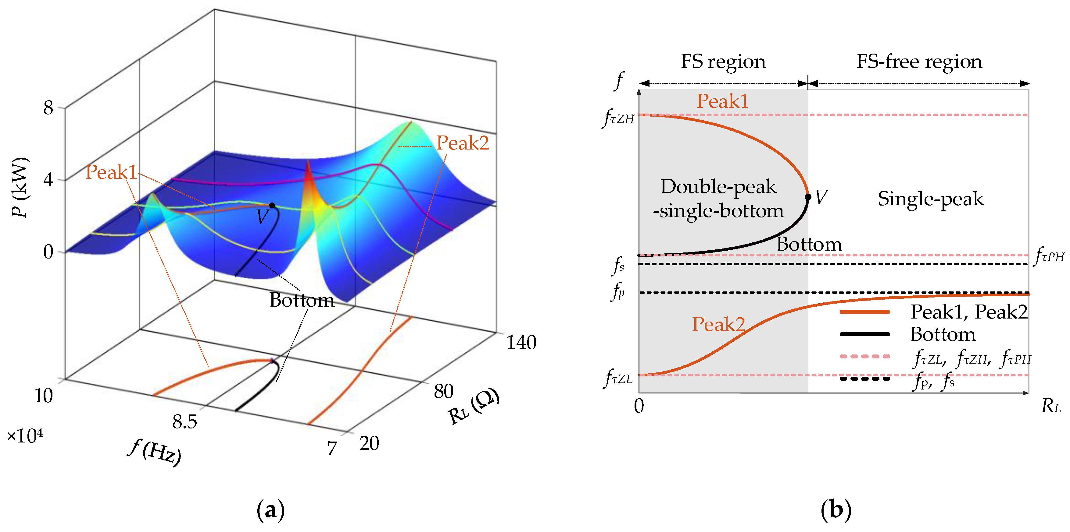
Taking f and RL as the variables, the 3D and 2D plots of the output power are given in Figure 3. On this power surface, there are two “mountains” with two peaks (denoted as Peak1 and Peak2 in the figure, corresponding to higher and lower splitting frequency, respectively) and one “valley” with one bottom line (denoted as Bottom in the figure). This aligns with the theory of frequency splitting, which is frequency splitting appears when the equivalent load resistance becomes lower, for a given coupling position (i.e., given k) [13]. Therefore, when RL is low, the output power has two peaks while scanning the operating frequency as shown in Figure 3. With larger RL, the output power has only one peak. The exact curves that describe the peaks and the bottom can be obtained by setting ∂P/∂f equal to 0, which is given by (8), and the detailed derivation process of (8) is provided in Appendix A.
R L 2 = L 2 2 k 2 - 1 - f p 2 f 2 1 - f s 2 f 2 k 2 - 1 - f p 2 + f s 2 f 2 + 3 f p 2 f s 2 f 4 f p 2 2 π 2 f 4 f p 2 f 2 - 1
In Figure 3, point V is the cross point of the Peak1 curve and the Bottom curve. The zone where RL < RV is the frequency splitting region, characterized by a double-peak-single-bottom feature, while the remaining area constitutes the frequency splitting-free zone exhibiting a single peak.

2.3. The Possible Charging Frequency Paths

Because the charging power is increasing in the CC mode as the battery voltage increases gradually, the operating frequency variation path of the CC mode should be like climbing one of the “mountains” in Figure 3. In other words, the operating frequency should be approaching one of the peak curves when the battery voltage increases (and also RL increases). In contrast, as the charging power is decreasing in the CV mode, the operating frequency path of the CV mode should walk down from the mountain, which means the operating frequency should shift away from the “peak” curve.
In Figure 4, three possible scenarios are given. In each scenario, the operating frequency paths lie within the shaded area, which guarantees the realization of ZVS. Point A and point B are the beginning of the CC and CV modes, respectively. Point C is the end of the CV mode. Point E is the cross point of the Bottom curve and the zero-phase angle curve. However, point E may not be reached in some cases, which will be discussed in Appendix B. fτPH is the frequency value of the cross point of the Bottom curve and vertical axis, which can also be obtained with (8).
In Figure 4a, the CC curve is above the Peak1 curve, and a monotonic control can be achieved. However, the frequency path is away from the optimal frequency path curve, which implies low system efficiencies.
In Figure 4b, the CC curve is between the Bottom curve and the Peak1 curve, while the CV curve shifts away from the Peak1 curve as RL increases. Point BCC and point BCV are the end of the CC mode and the beginning of the CV mode, respectively, which have the same RL value. At a certain coupling position with a certain coupling coefficient, point BCC and point BCV overlap on the Peak1 curve, and a monotonic and continuous control can be realized. However, at other different coupling positions, point BCC and point BCV are separated by the Peak1 curve, and thus, a continuous control becomes impossible.
In Figure 4c, both the CC curve and part of the CV curve are between the Bottom curve and the Peak2 curve, which makes it possible to achieve a monotonic and continuous control while staying close to the OFP curve. Therefore, the operating frequency path in the last scenario is chosen as the optimal one for the CC/CV control of SS WPT systems.

2.4. CC f-RL Path of Charging Frequency Path

The CC f-RL curve of the CC mode can be derived as
ω 2 M 2 V i n 2 R L ω 2 M 2 - X 1 X 2 2 + R L 2 X 1 2 = I c c 2 R L
where Icc is the constant current value. Then, (10) can be derived from (9), and the derivation process appears in Appendix C.
R L 2 = k 2 L 2 V in 2 - 4 π 2 f 2 L 1 L 2 2 I cc 2 k 2 - 1 - f p 2 f 2 1 - f s 2 f 2 2 L 1 I cc 2 1 - f p 2 f 2 2
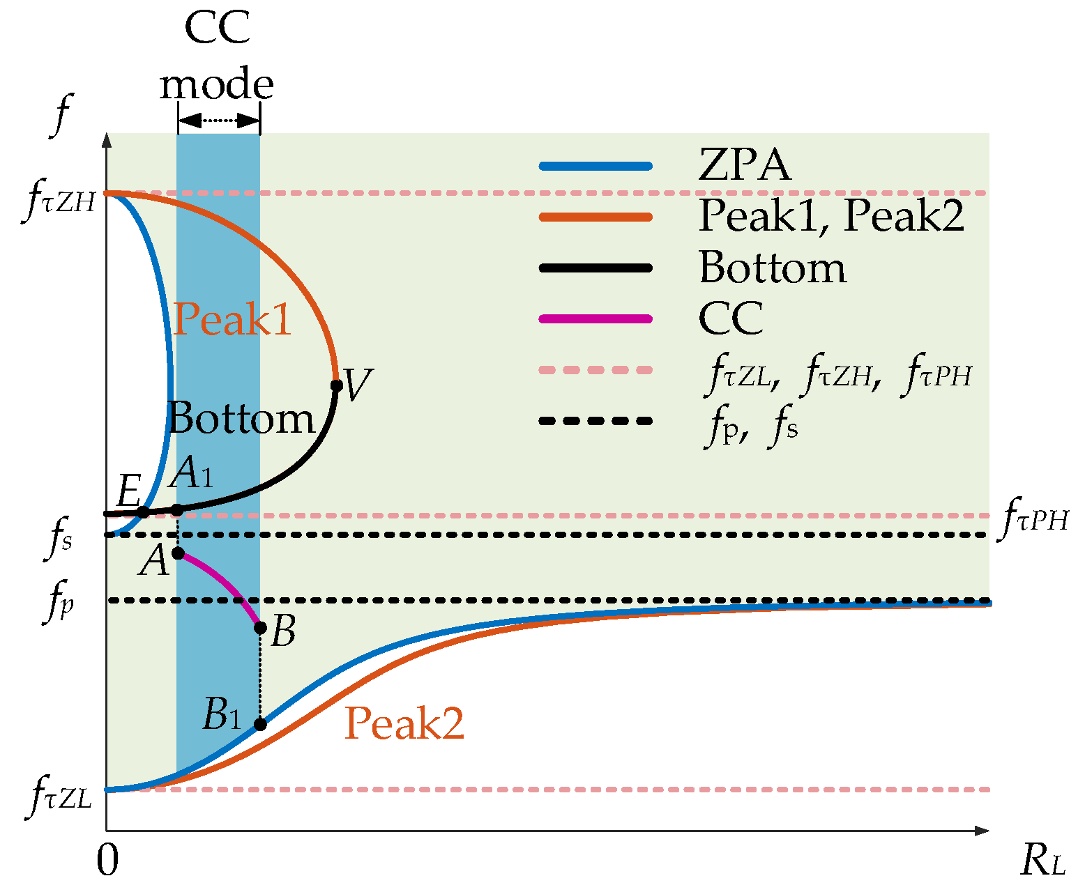
A typical CC f-RL curve (AB) is plotted in Figure 5 based on (10). Point A1 is on the Bottom curve and has the same RL as point A. Similarly, point B1 has the same RL as point B. In another case, when RA < RE, point A1 should be on the zero-phase angle curve.
In the CC mode, as RL increases, the CC f-RL curve approaches the Peak2 curve, resulting in a rising output power. In Figure 5, when RARV, point A is located within the region between the Bottom curve and the Peak2 curve, where fA is close to fs, which helps to increase the system efficiency.
Therefore, to achieve a monotonic frequency control and a high-efficiency operation in the CC mode, there are three constraints given as follows:
(1)
PA1Pstart, where PA1 means the output power at point A1, which is the minimum output power that can be achieved by the system at RA; Pstart means the required output power at the start point of the CC mode.
(2)
PB1Prated, where PB1 means the output power at point B1, which is the maximum output power that can be achieved by the system at RB; Prated means the required output power (i.e., the rated power) at the end of the CC mode.
(3)
RARV.

2.5. CV f-RL Path of Charging Frequency Path

The relationship between RL and f in the CV mode is given by
ω 2 M 2 V i n 2 R L ω 2 M 2 - X 1 X 2 2 + R L 2 X 1 2 = U c v 2 R L
where Ucv is the constant voltage value. Similarly, (12) can be derived from (11), and Appendix C gives the full derivation.
R L 2 = 4 π 2 f 2 L 1 L 2 2 U cv 2 k 2 - 1 - f p 2 f 2 1 - f s 2 f 2 2 k 2 L 2 V i n 2 L 1 U c v 2 1 f p 2 f 2 2
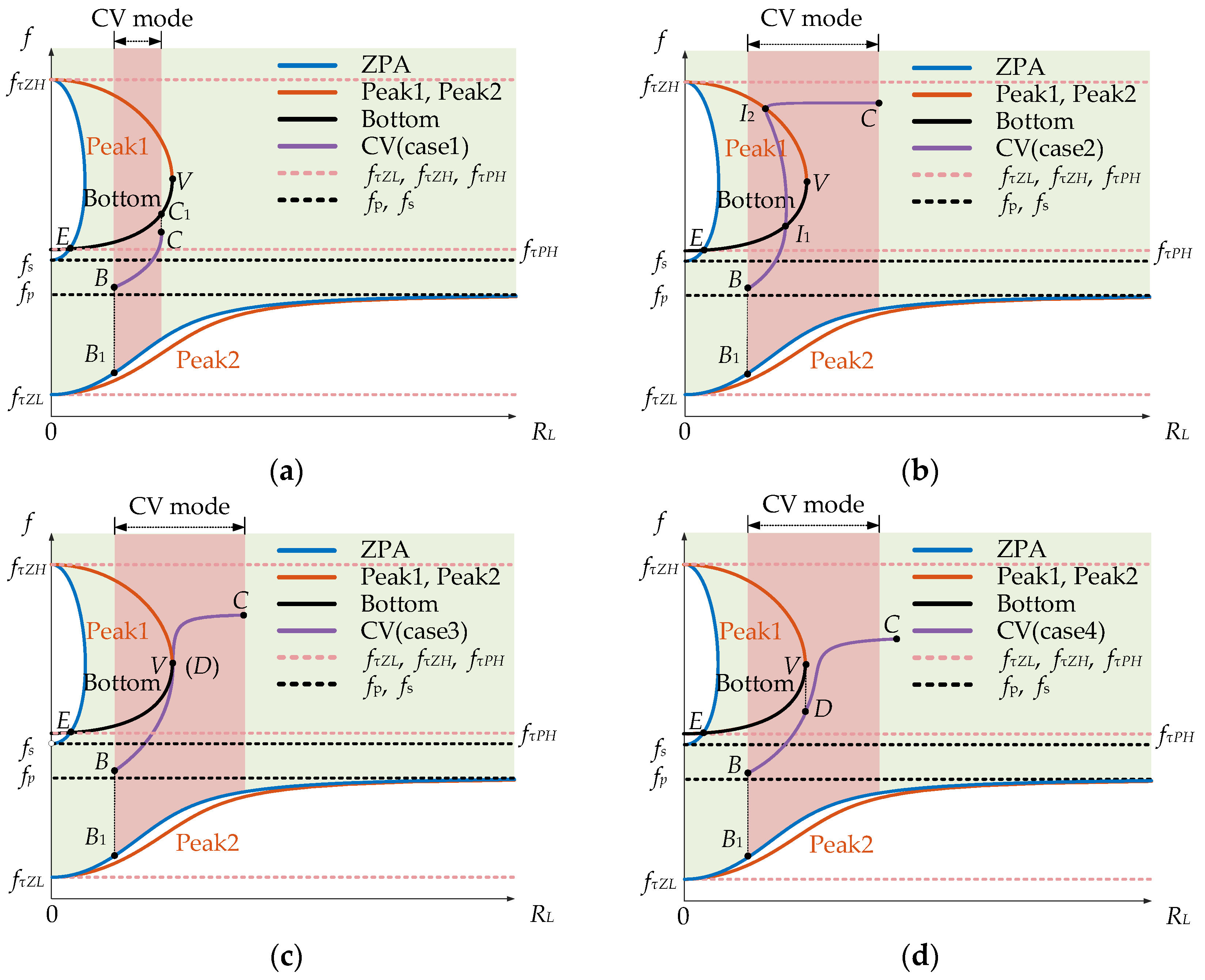
Four typical CV f-RL curves are plotted in Figure 6 based on (12). Point I1 and point I2 are the cross points of the CV f-RL curves with the Bottom curve and the Peak1 curve, respectively. Point C1 is on the Bottom curve, and it has the same RL as point C, while point D is on the CV curve, and it has the same RL as point V.
  • When RC < RV, the possible f-RL curve is given in Figure 6a. In this case, the CV f-RL curve lies between the Bottom curve and the Peak2 curve, and the power decreases as the frequency increases. Then, the constraints can be summarized as follows:
    (1)
    fCfC1.
    (2)
    PC1Pend, where PC1 means the output power of the system at point C1, which is the minimum achievable power of the system at RC; Pend means the required output power at the end of the CV mode (i.e., at point C).
  • When RCRV, there are three possible CV f-RL curves:
    (1)
    For case2 (Figure 6b), the f-RL curve penetrates the Peak1, which implies a continuous control is not possible.
    (2)
    For case3 (Figure 6c) and case 4 (Figure 6d), RL and f increase simultaneously, and the CV f-RL curves move away from the Peak2 curve. Case3 can be regarded as a critical case between case2 and case4.
  • In summary, when RCRV, there is only one requirement to meet to realize monotonic and continuous frequency control, which is fDfV.

3. Parameter Design

According to the theory described in Section 2, the charging frequency path lies entirely within the shaded region; the problem of ZVS loss will consequently be solved. Hence, to achieve monotonic and continuous frequency control, there are a total of four constraints, given as
(1)
PA1Pstart.
(2)
PB1Prated.
(3)
RARV.
(4)
PC1Pend when RC < RV or fDfV when RCRV.
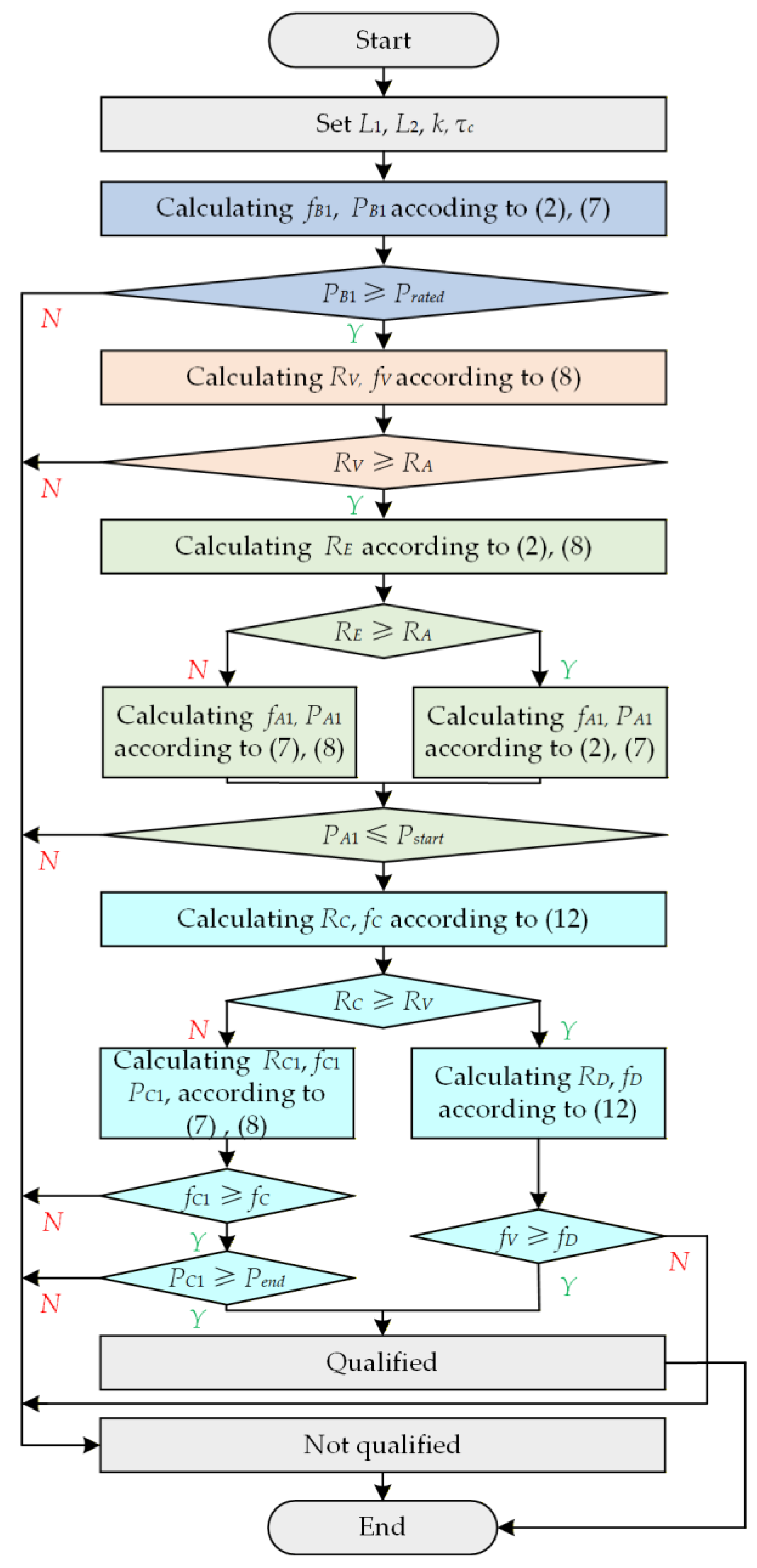
In this paper, fp is set to 80 kHz. The coupling coefficient k varies in the range of [0.1, 0.3]. With certain step sizes, every combination of [L1, L2, k, τc] will be tested through the flowchart in Figure 7 to judge whether the combination meets the above constraints. According to the finite element analysis simulation, the maximum inductance value that can be achieved after the coil is tightly wound is approximately 813.6 μH. To simplify the winding of coils, both L1 and L2 are assumed to be in the range of [300 μH, 810 μH]. The specifications of the prototype system are given in Table 2.
From (4), it can be known that fτzL increases as τc decreases, which means that the region between the Bottom curve and the Peak2 curve becomes narrower with a smaller τc, making the CC f-RL curve more likely to approach the curve f = fs and improve system efficiency. Therefore, the minimum τc is set to 1.01.
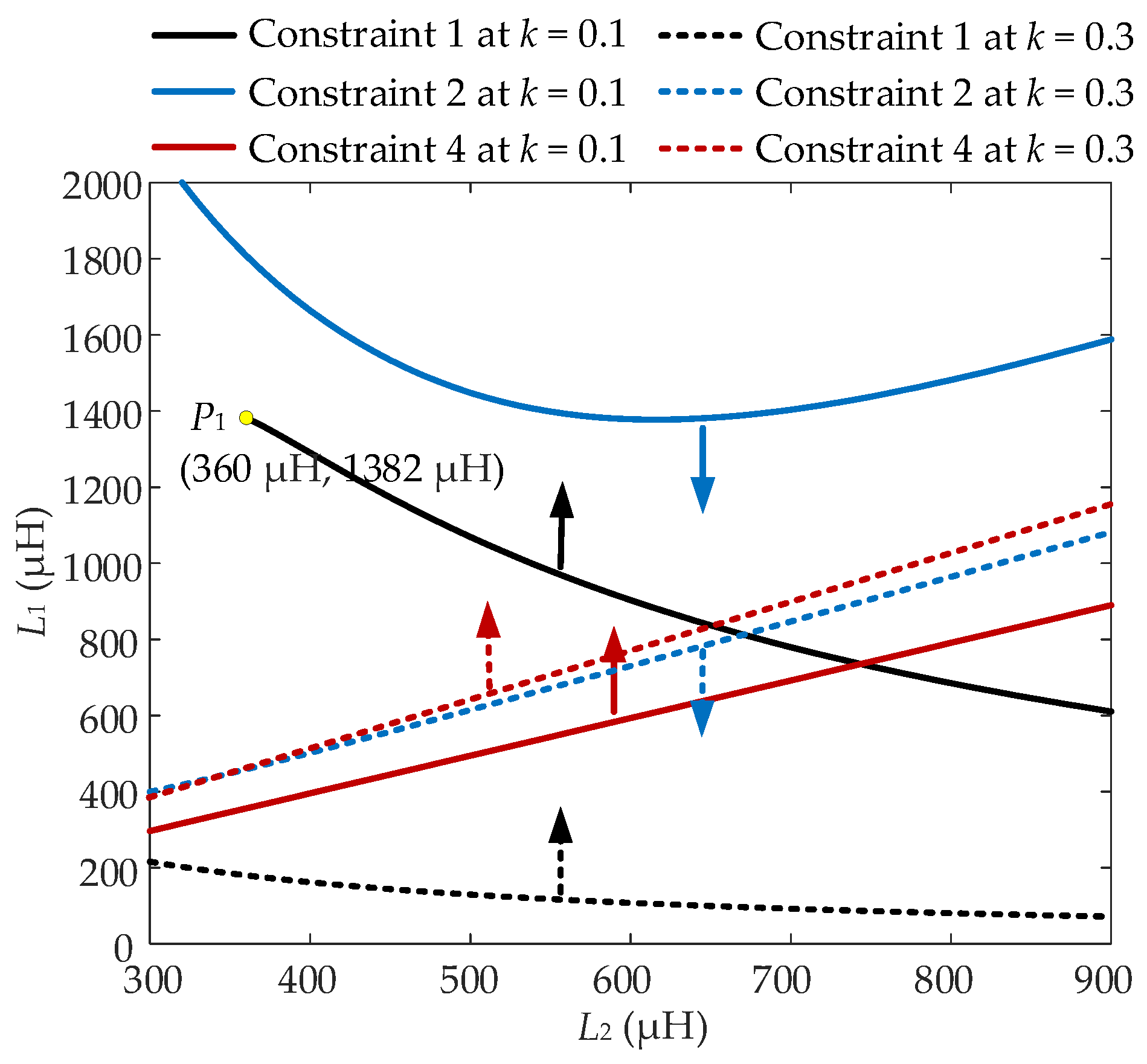
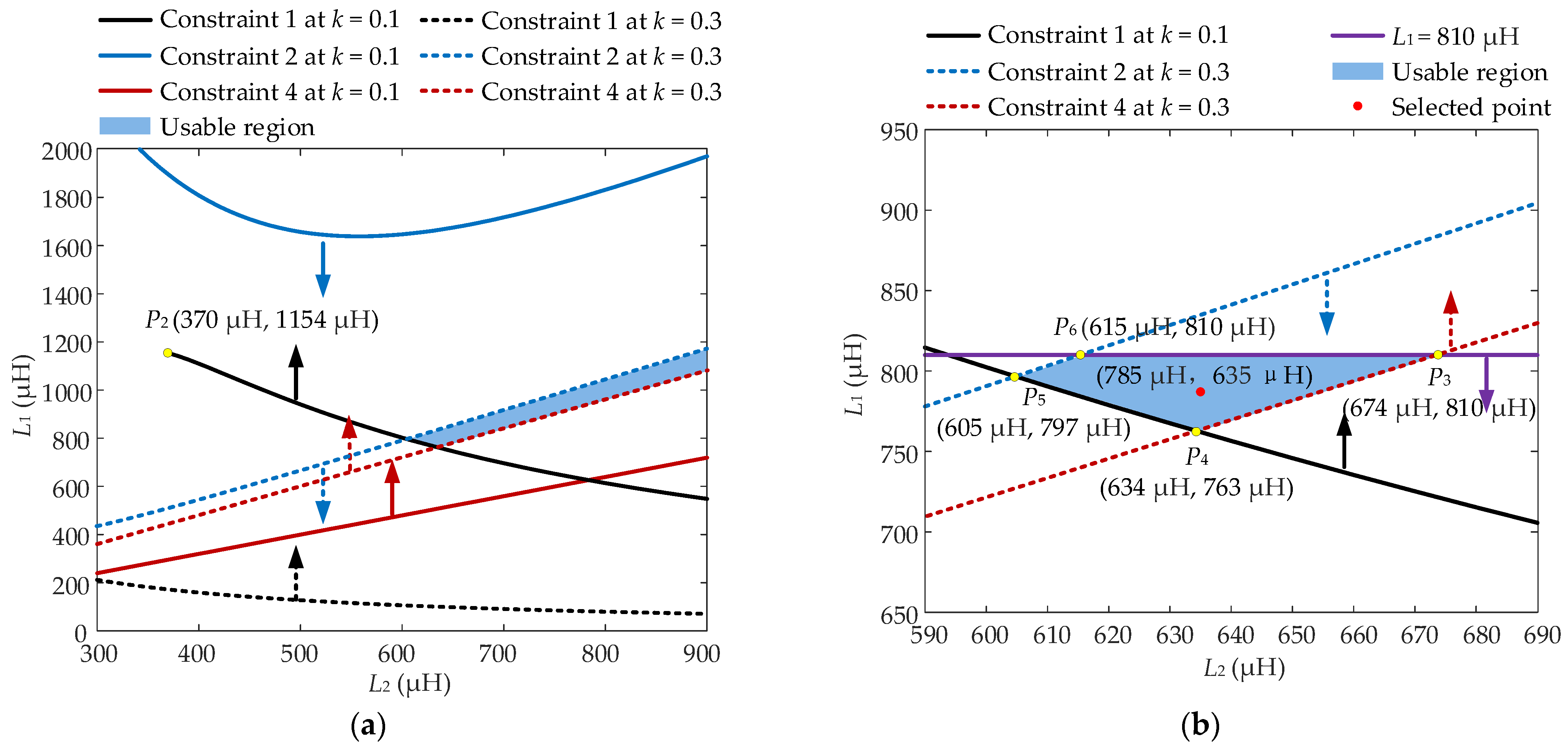
In this paper, the minimum value of L2 required to achieve RC < RV is denoted as L2C-V, while the minimum value of L2 required to achieve RARV is denoted as L2A-V, which are given in Table 3. Table 3 indicates that, within the inductance range of [300 μH, 810 μH], only RCRV needs to be taken into consideration. The results of Figure 7 indicate that no parameter combinations can be found to meet the above four requirements when τc is 1.01 or 1.02. The constraint curves with τc values of 1.02 and 1.03 are shown in Figure 8 and Figure 9, respectively. The regions aligned with the arrow directions and enclosed by the constraint curves in Figure 8 and Figure 9 indicate the areas where the corresponding constraint conditions are met. Figure 2 indicates that τc = 1 represents the critical state of the zero-phase angle boundary, where the two ZVS regions just become connected. As τc increases, the connecting channel between two regions widens, resulting in an expanded design space. This explains why no feasible region can be identified until τc reaches 1.03. Eventually, a usable design is determined as L1 = 785 μH and L2 = 635 μH, which is within the usable region.

4. Experimental Verification

4.1. Description of the Prototype

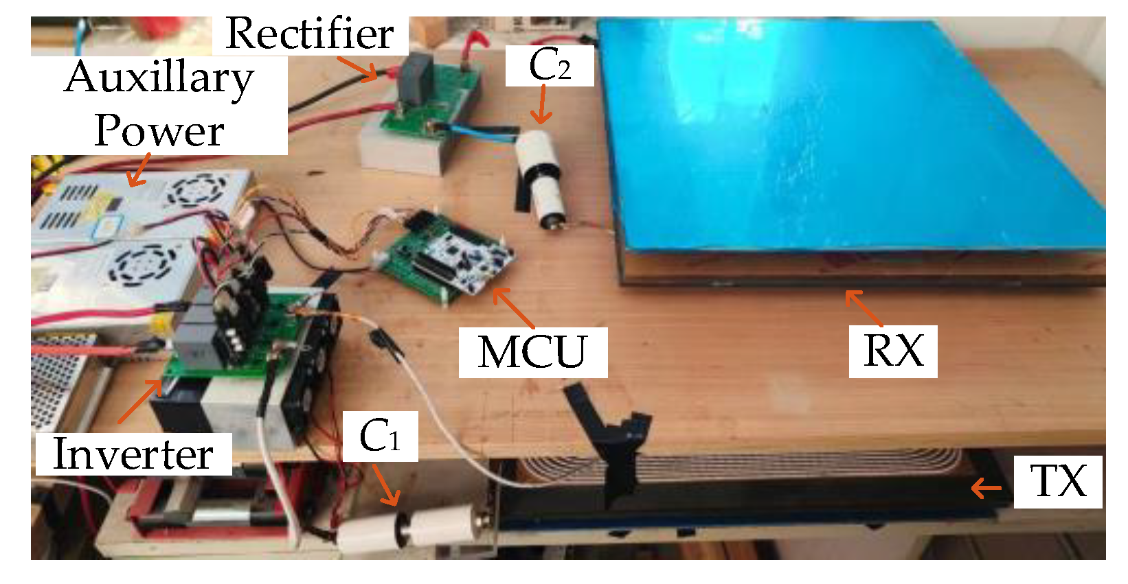
According to Figure 1a, a prototype is built as shown in Figure 10. The SiC MOSFET C3M0021120D from CREE is used for the inverter, and the diode RURG80100 from ON Semiconductor is used for the rectifier. The system parameters are given in Table 4. The values of L1 and L2 were obtained in Section 3. With (3), the values of C1 and C2 can, therefore, be calculated. By performing finite element simulations with different numbers of turns, as shown in Figure 11, the primary and secondary coil turns, N1 and N2, that most closely match the required L1 and L2 values, respectively, can be determined.
Figure 11 shows the transmitting side and the receiving side of the prototype system. The parameters of the coils are given in Table 5, where dcf is the distance between the coil and the ferrite core and daf is the distance between the aluminum layer and the ferrite core.

4.2. Experimental Results

To verify the proposed control and design method, 30 operation points (10 for kmax = 0.3, 10 for kmid = 0.2, and 10 for kmin = 0.1) are selected for the 3.3 kW experiment group. RLDC at 3.3 kW is 48.5 Ω, which is denoted as RLrated. RLDC for different operating points are 0.5RLrated, 0.6RLrated, 0.7RLrated, 0.8RLrated, 0.9RLrated, RLrated, 2RLrated, 3RLrated, 4RLrated, and 5RLrated, respectively. These load resistance values can be accurately obtained using the constant resistance mode of the electronic load.
To enhance the practicality of the proposed method, the designed system should be able to work with different specifications. As introduced in Section 3, the charging process can be accomplished as long as the system meets the four constraints of the target charging condition. To verify this, another 30 operation points are conducted for the 2.4 kW experiment group. The CV mode of electronics load is used, which can better simulate the real charging process, and the parameters are listed in Table 6.
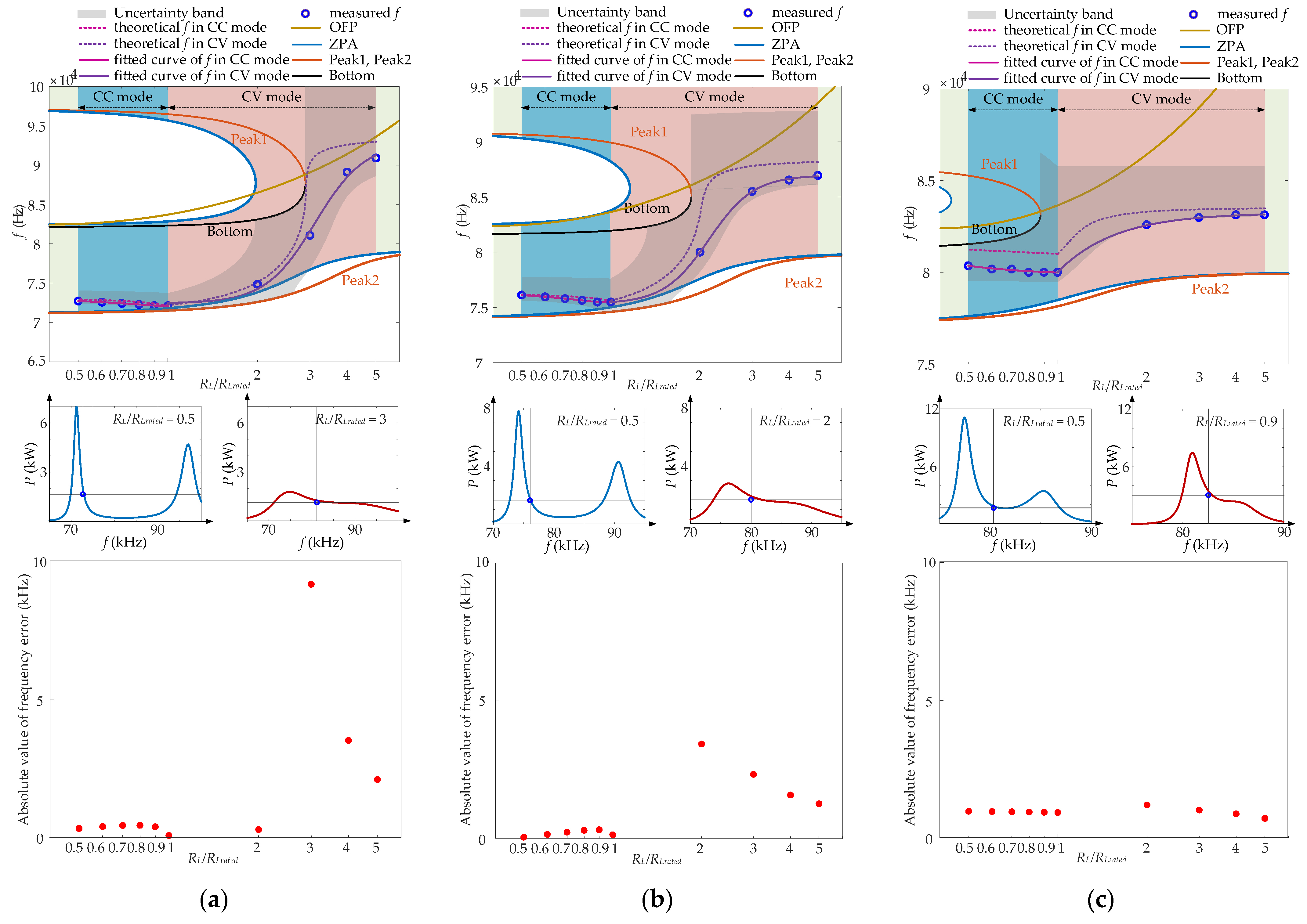
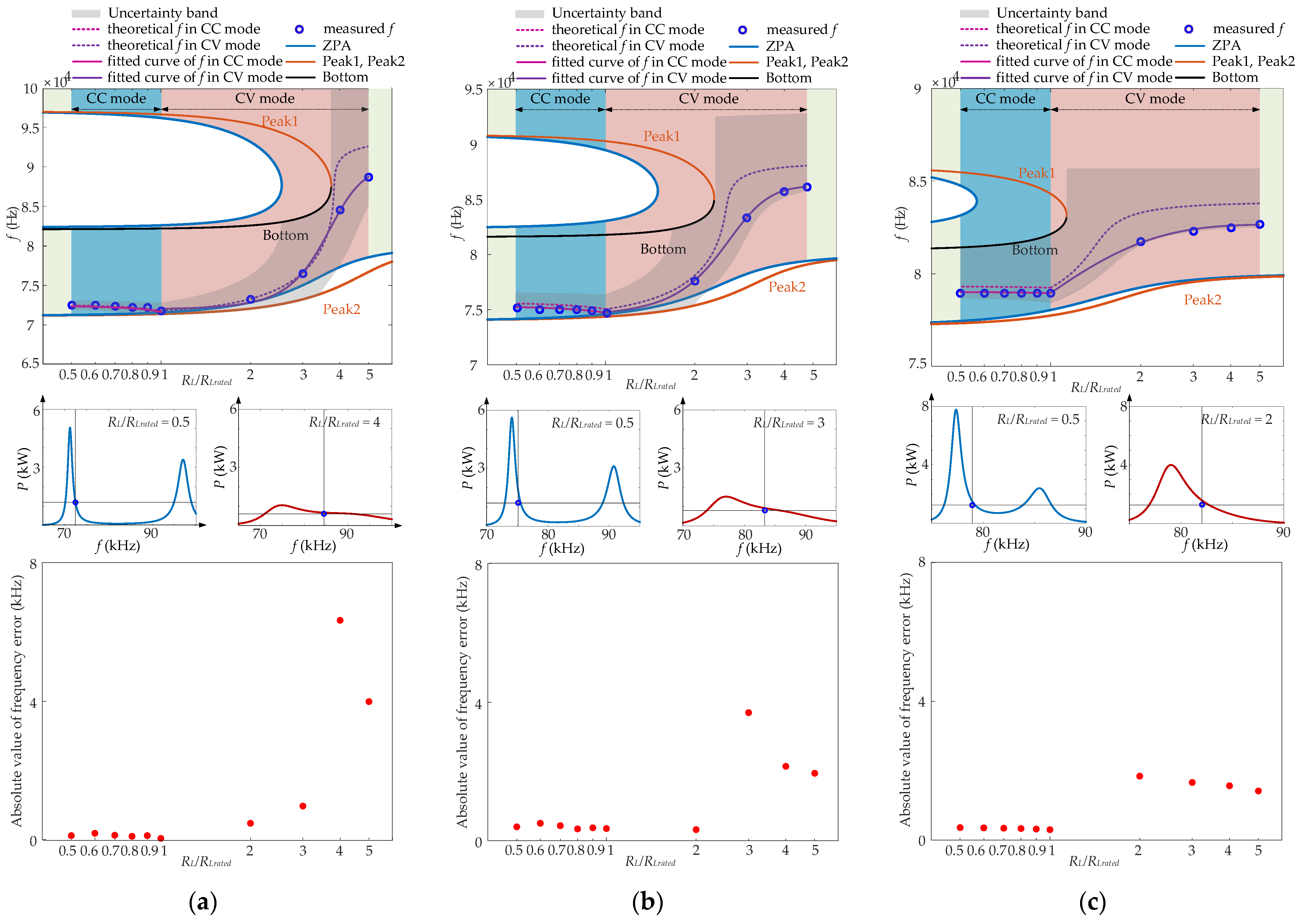
Figure 12 and Figure 13 give the theoretical operating frequency curves and the measured operating frequency points for both 3.3 kW and 2.4 kW experiment groups, respectively. As shown in Figure 12, the OFP curve is presented. Compared to the cases of k = 0.3 and k = 0.2, the constant current curve for k = 0.1 is closer to the OFP curve. This characteristic, to some extent, mitigates the efficiency drop caused by weak coupling and demonstrates the necessity of the constraint RARV. The theoretical P-f variation curves corresponding to the loads at both the CC charging initiation point and the experimental point near point V are also provided in Figure 12 and Figure 13, which verifies that the frequency path indeed crosses from the frequency splitting region between two splitting frequencies to the frequency splitting-free region. The measured CC/CV f-RL curves are all located at the designated area, which guarantees the monotonicity and continuity of the control. The actual operating frequencies are slightly lower than the theoretical values because losses are not included in the calculation in (7). Compared to the cases with k = 0.2 and 0.3, the f-RL curve of k = 0.1 in CC mode is closer to the Bottom curve (see the P-f curve with RL/RLrated = 0.5 in Figure 12c), where the output power changes more slowly with the operating frequency. As a result, the power losses neglected in the calculation will lead to larger differences between the measured frequency values and the theoretical frequency values.
To better demonstrate the stability of the proposed method, the frequency errors between theoretical and measured frequency values, along with the corresponding uncertainty bands (grey shaded regions), have been added to Figure 12 and Figure 13. The grey shaded region surrounding the theoretical curve represents the 99% confidence interval of the predicted values, quantifying the combined uncertainties from measurement systems and parameter estimation. The upper and lower boundaries are calculated through the expressions Pupperbound = P + Zvalue × stderror and Plowerbound = PZvalue × stderror, where P denotes the theoretical output power and stderror corresponds to a 20% relative uncertainty of the theoretical power value. This is because the minimum measured efficiency in the experiment is close to 80%, implying that a maximum of 20% of the power is dissipated as losses in the experimental points. Zvalue = 2.58 defines the 99% confidence level under normal error distribution assumptions. With (7), the frequencies corresponding to Pupperbound and Plowerbound, namely flowerbound and flowerbound, can be derived. The partial overlap of the grey shaded region’s boundary with the Peak2 curve indicates that even the power along Peak2 also cannot exceed 120% of the required power. Similarly, the overlap with the Bottom curve signifies that the power on the Bottom curve cannot fall below 80% of the required power. For the remaining boundaries that do not coincide with these curves, the corresponding frequencies have a 99% probability of delivering power precisely within the range of ±20% of the required value. All experimental points are in the grey shaded region. The experimental points that have large frequency errors correspond to load resistances where the output power changes very gradually with frequency. In such operating regimes, even minor variations in power loss can lead to proportionally larger shifts in the operating frequency. It can be found that the frequency errors for most experimental points are acceptable, which validates the effectiveness of the proposed method.
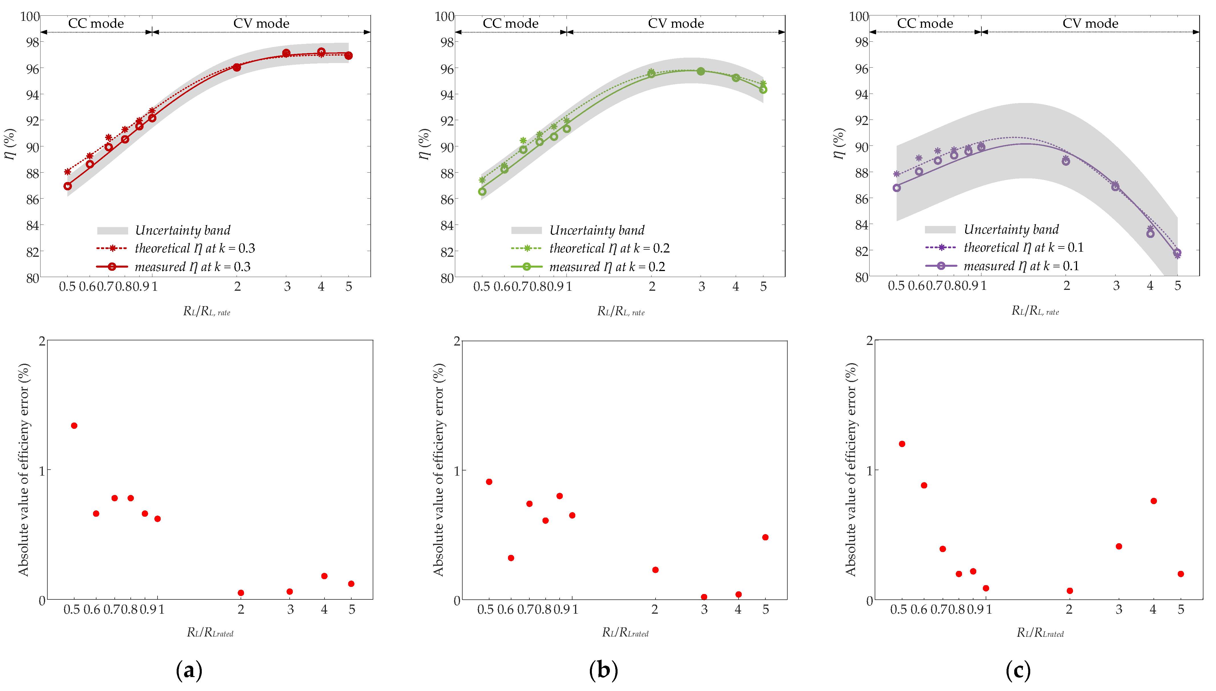
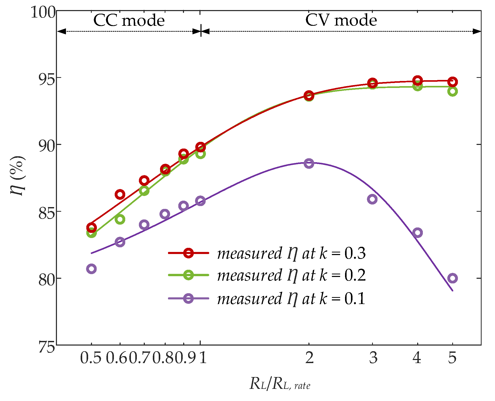
The DC-DC efficiencies for both 3.3 kW and 2.4 kW experiment groups are given in Figure 14 and Figure 15, respectively. The measured DC-DC efficiency ranges for rated power are 89.9–92.1% and 85.8–89.8%, respectively. The theoretical efficiencies for the 3.3 kW experiment group in Figure 14 are derived from the loss analysis presented in the following Part. Since the loss analysis for the 3.3 kW experimental group has been thoroughly conducted, the theoretical efficiency calculation is not repeated for the 2.4 kW experiment group.
Uncertainty bands and efficiency deviations have also been incorporated into Figure 14. The uncertainty bands are computed using the formula y f i t ± t α / 2 , n 1 s 1 + 1 / n , where yfit represents the values of the measured efficiency fitted curve; tα/2,n−1 is the critical value from the Student’s t-distribution, where α = 0.01 (99% confidence level, tα/2,n−1 = 3.25 in this paper) and n is the number of experimental data points (n = 10 in this study); s is the standard deviation of residuals between experimental data points and the fitted curve; and the term 1 + 1/n incorporates the additional uncertainty when predicting new observations beyond the existing dataset. There are only a few individual theoretical points, particularly in the low-resistance region. The reason is that the switching frequency in this work ranges from 72 to 91 kHz, whereas the equivalent series resistance (ESR) values of the coils and capacitors used for the efficiency calculation are measured at a fixed frequency of 80 kHz. The frequencies corresponding to the theoretical points outside the grey shaded region deviate from 80 kHz, leading to a discrepancy between the actual ESR and the value used in the theoretical efficiency calculation model. Consequently, a small number of theoretical efficiency points fall outside the grey uncertainty bands. It can be observed that the discrepancy between the theoretical and measured efficiency does not exceed 1.4% for all measurement points. This finding further attests to the effectiveness and reliability of the proposed method. To avoid redundancy, the efficiency errors and uncertainty bands are not calculated for Figure 15.
The measured and the theoretical input impedance angles, i.e., θin, for each operation point in the 3.3 kW experimental group are summarized in Table 7. The measured range of θin is 8–72°, which is in good agreement with the theoretical values considering that the losses in the inverter, rectifier, shield, core, etc., are not included in the theoretical model. The minimum input impedance angle required for robust ZVS is determined by the energy balance during dead time. The critical angle θZVSmin is calculated to ensure sufficient inductor current to discharge the MOSFET junction capacitances. The critical angle can be calculated as θZVSmin = arcsin(2CossVDC/tdeadAm), where Coss is the MOSFET output capacitance, VDC is the DC input voltage, tdead is the dead time, and Am is the amplitude of the primary current. In this paper, for the rated power, the four system parameters are given as Coss = 200 pF, VDC = 400 V, tdead = 450 ns, and Am = 13.4 A (13.4 A is the minimum measured current value). Then, θZVSmin can be derived as 1.5°. From Table 7, it is clear that ZVS can be achieved over the entire coupling range and load range, as the minimum angle (8°) provides a sufficient margin to ensure its realization. The waveforms of the inverter output voltage and output current are given in Figure 16 at the rated power for the 3.3 kW experimental group, also verifying ZVS operation.

4.3. Loss Analysis

Figure 17 gives the system loss breakdown of rated power at kmax, kmid, and kmin for the 3.3 kW experimental group, which indicates that the main losses are from the resonators. The core loss and shield loss are obtained through the volume integral of ohmic loss over the ferrite core and aluminum shield with finite element analysis simulation. According to the RURG80100 datasheet, the voltage–current relationship of the diode at 100 °C can be expressed as (13), where IF represents the diode forward current and VF represents the diode forward voltage. Meanwhile, IF also represents the sinusoidal current flowing through the secondary coil, which can be expressed as (14), where Am denotes the current amplitude, and it can be calculated with the method introduced in [25]. For the 3.3 kW prototype, Am is 12.96 A at rated power. Within a single operating cycle of one diode, the power loss can be calculated as the integral of IF multiplied by VF over the interval [0, π/ω]. During each full operating cycle, this heat generation process is repeated across four diodes. Therefore, (15) can be employed to compute the total rectifier losses. The ZVS turn-on is achieved; thus, the MOSFET turn-on losses are neglected. The amplitudes of i1 in Figure 16a–c for 3.3 kW experimental group are 13.4 A, 14.6 A, and 17.4 A, respectively. The dead time accounts for a very small portion of the entire current variation cycle. For simplicity, the current during the dead time is treated as a constant value in this work. With the i1 amplitudes and the θin values in Table 7, the MOSFET current values at turn-off can be calculated to be less than 10 A. According to the C3M0021120D datasheet, the turn-off losses of the MOSFET at these current values can also be neglected. The calculation methods for the conduction losses of the MOSFET Pcon are given by (16). According to [26], the conduction losses of the parallel diode PDcon and the reverse recovery losses Pres are provided by (17) and (18). The loss of the capacitors and the coils can be directly calculated with the data given in Table 8, using P = I r m s 2 R , where R can represent the equivalent series resistance of coil or capacitor. The calculated loss values corresponding to kmax, kmid, and kmin are 259 W, 289 W, and 367 W, respectively, while the measured loss values are 283 W, 314 W, and 371 W. The difference between the two is acceptable.
V F = 0.000152384 I F 3 - 0.00481 I F 2 + 0.06724 I F + 0.57539
I F = A m sin ω t
P r e c t i f i e r = 2 f 0 ω π V F I F dt
P c o n = A m 2 R D S ( O N ) - 4 A m 2 sin ( θ ) 2 R D S ( O N ) t d e a d f
P Dcon = 4 A m sin ( θ ) V D M t d e a d f
P r e s = 2 Q r r V D M

5. Conclusions

In this article, the secondary-side resonant frequency is designed to be higher than the primary-side resonant frequency to facilitate the realization of ZVS in the SS WPT system. Following the derivation of the power transfer characteristics, a key conclusion for achieving high efficiency is that the operating frequency in CC mode should be as close as possible to the secondary-side resonant frequency. Based on these principles, a systematic parameter design flow is established, and an experimental prototype is constructed. A monotonic and continuous frequency control can be achieved to output the required power in both CC and CV modes, even with coil misalignment. Using the same experimental setup, both 3.3 kW and 2.4 kW experiment groups are conducted to demonstrate the effectiveness and performance of the proposed method. The experimental results show that the WPT system can maintain ZVS across a coupling coefficient range of [0.1, 0.3] and a load resistance variation of up to 10:1. The overall efficiency of the 3.3 kW experiment group ranges between 81.8% and 97.2%, and the efficiency drop is only 2.2% under a 3:1 coupling variation at rated power. Several aspects of the present work can be further improved. For example, to ensure accuracy in theoretical efficiency calculations across a broad frequency range, the frequency-dependent ESR of components must be accounted for at each specific operating point. Using a fixed set of ESR values measured at one frequency can otherwise lead to substantial deviations from the measured results. For practical WPT applications, parameter drift and temperature variations are critical factors that must be considered. In future work, these aspects will be incorporated prior to the system parameter design phase.

Author Contributions

Y.L., W.Z. and K.Y. developed the idea of this study; Y.L. conducted the calculations, experiments, and data analysis; Y.L., M.L. and W.Z. revised the manuscript. All authors have read and agreed to the published version of the manuscript.

Funding

This research received no external funding.

Data Availability Statement

Data are contained within the article.

Conflicts of Interest

The authors declare no conflicts of interest.

Appendix A

X1 and X2 can be expressed as
X 1 = ω L 1 1 - ω p 2 ω 2 X 2 = ω L 2 1 - ω s 2 ω 2
Then, ∂P/∂ω can be calculated as (A2),
P ω = - 2 k 2 L 2 R L V i n 2 A L 1 R L 2 ω 3 - ω p 2 ω 2 + L 2 2 k 2 - 1 ω 4 + ω p 2 + ω s 2 ω 2 - ω p 2 ω s 2 2 2 A = ω 5 2 R L 2 ω 2 ω p 2 ω 2 - ω p 2 + L 2 2 k 2 - 1 ω 4 - ω p 2 + ω s 2 ω 2 + 3 ω p 2 ω s 2 k 2 - 1 ω 4 + ω p 2 + ω s 2 ω 2 - ω p 2 ω s 2
and (8) can be obtained through setting A = 0.

Appendix B

The coordinates of point E can be obtained from the ZPA Equation (2) and the Bottom curve Equation (8), as shown below:
f E = f p 2 - f s 2 + f p 2 + f s 2 2 - 4 k 2 f p 2 f s 2 2 1 - k 2 R E = 8 π 2 f s 2 L 2 2 f p 2 + 2 k 2 f s 2 - 3 f s 2 + f p 2 + f s 2 2 - 4 k 2 f p 2 f s 2 f p 2 - f s 2 + f p 2 + f s 2 2 - 4 k 2 f p 2 f s 2
The numerator of fE and the denominator of RE are identical and always positive. Due to space limitations, the proof is omitted here. When RE > 0, it follows that τ c < 2 2 k 2 . Therefore, for k ∈ [0.1, 0.3], as long as τc > 1.024, the zero-phase angle curve will not intersect with the Bottom curve, and point E will not exist.

Appendix C

Equation (A4) can be directly derived from (9):
R L 2 = k 2 L 2 V i n 2 ω 6 I c c 2 L 1 L 2 2 k 2 1 ω 4 + ω p 2 + ω s 2 ω 2 ω p 2 ω s 2 2 L 1 I c c 2 ω 2 ω 2 ω p 2 2
Similarly, (A5) can be obtained from (11):
R L 2 = L 1 L 2 2 U c v 2 k 2 ω 4 - ω 2 - ω p 2 ω 2 - ω s 2 2 k 2 L 2 V i n 2 ω 6 - L 1 U c v 2 ω 2 ω 2 - ω p 2 2
Equation (10) can be derived by dividing both the numerator and denominator of (A1) by ω6, and (12) can be obtained from (A5) in the same way.

References

  1. Si, P.; Hu, A.P.; Malpas, S.; Budgett, D. A Frequency Control Method for Regulating Wireless Power to Implantable De-Vices. IEEE Trans. Biomed. Circuits Syst. 2008, 2, 22–29. [Google Scholar] [CrossRef] [PubMed]
  2. Narayanamoorthi, R.; Juliet, A.V.; Chokkalingam, B. Frequency Splitting-Based Wireless Power Transfer and Simultaneous Propulsion Generation to Multiple Micro-Robots. IEEE Sens. J. 2018, 18, 5566–5575. [Google Scholar] [CrossRef]
  3. Panhwar, I.H.; Mekhilef, S.; Seyedmahmoudian, M.; Soon, T.K.; Mokhlis, H.; Stojcevski, A. Digital Phase Synchronization and Wireless Communication in a Bidirectional SS-Compensated Wireless Power Transfer System for Electric Vehicles. IEEE Trans. Transp. Electrif. 2025, 11, 13619–13630. [Google Scholar] [CrossRef]
  4. Zhong, W.X.; Hui, S.Y.R. Maximum Energy Efficiency Tracking for Wireless Power Transfer Systems. IEEE Trans. Power Electron. 2015, 30, 4025–4034. [Google Scholar] [CrossRef]
  5. Jiang, Y.; Wang, L.; Fang, J.; Li, R.; Han, R.; Wang, Y. A High-Efficiency ZVS Wireless Power Transfer System for Electric Vehicle Charging with Variable Angle Phase Shift Control. IEEE J. Emerg. Sel. Topics Power Electron. 2021, 9, 2356–2372. [Google Scholar] [CrossRef]
  6. Li, H.; Fang, J.; Chen, S.; Wang, K.; Tang, Y. Pulse Density Modulation for Maximum Efficiency Point Tracking of Wireless Power Transfer Systems. IEEE Trans. Power Electron. 2018, 33, 5492–5501. [Google Scholar] [CrossRef]
  7. Li, Y.; Hu, J.; Chen, F.; Li, Z.; He, Z.; Mai, R. Dual-Phase-Shift Control Scheme with Current-Stress and Efficiency Optimization for Wireless Power Transfer Systems. IEEE Trans. Circuits Syst. I Reg. Pap. 2018, 65, 3110–3121. [Google Scholar] [CrossRef]
  8. Cheng, L.; Ki, W.-H.; Lu, Y.; Yim, T.-S. Adaptive On/Off Delay-Compensated Active Rectifiers for Wireless Power Transfer Systems. IEEE J. Solid-State Circuits 2016, 51, 712–723. [Google Scholar] [CrossRef]
  9. Meshram, V.S.; Corti, F.; Solimene, L.; Musumeci, S.; Ragusa, C.S.; Reatti, A. Variable Inductor Control Strategy in LCC-S Compensated Wireless Power Transfer Application. In Proceedings of the 2023 AEIT International Annual Conference (AEIT), Rome, Italy, 5–6 October 2023; pp. 1–6. [Google Scholar]
  10. Lai, C.-M.; Hsu, C.-H.; Lin, Y.-C.; Chen, M.-Z.; Zheng, T.-Z. A High-Efficiency Wireless Power Transfer System with Variable Capacitor Technique for Compensating Coil Misalignment. In Proceedings of the 2024 IEEE Wireless Power Technology Conference and Expo (WPTCE), Seoul, Republic of Korea, 4–7 June 2024; pp. 688–692. [Google Scholar]
  11. Deng, S.; Liao, J.; Chen, Q.; Luo, P.; Zhang, G. Variable-inductance/capacitance-based Control Strategy for on-road EV with Constant Power Wireless Charging. In Proceedings of the 2023 IEEE PELS Students and Young Professionals Symposium (SYPS), Nanjing, China, 5–6 August 2023; pp. 1–5. [Google Scholar]
  12. Mai, R.; Chen, Y.; Li, Y.; Zhang, Y.; Cao, G.; He, Z. Inductive Power Transfer for Massive Electric Bicycles Charging Based on Hybrid Topology Switching with a Single Inverter. IEEE Trans. Power Electron. 2017, 32, 5897–5906. [Google Scholar] [CrossRef]
  13. Sample, A.P.; Meyer, D.T.; Smith, J.R. Analysis, Experimental Results, and Range Adaptation of Magnetically Coupled Resonators for Wireless Power Transfer. IEEE Trans. Ind. Electron. 2011, 58, 544–554. [Google Scholar] [CrossRef]
  14. Niu, W.-Q.; Chu, J.-X.; Gu, W.; Shen, A.-D. Exact Analysis of Frequency Splitting Phenomena of Contactless Power Transfer Systems. IEEE Trans. Circuits Syst. I Reg. Pap. 2013, 60, 1670–1677. [Google Scholar] [CrossRef]
  15. Zheng, C.; Ma, H.; Lai, J.; Zhang, P. High-Efficiency Contactless Power Transfer System for Electric Vehicle Battery Charging Application. IEEE J. Emerg. Sel. Topics Power Electron. 2015, 3, 65–74. [Google Scholar] [CrossRef]
  16. Onai, M.; Ojo, O. Performance Analysis and Design of Frequency Controlled Series-Series Compensated Inductive Power Transfer System for Electric Vehicle Battery Charging. IEEE Trans. Ind. Appl. 2022, 58, 962–973. [Google Scholar] [CrossRef]
  17. Chen, W.; Liu, Z.; Liu, J.; Su, H. Analysis and Design of Wireless Charging Systems Without Extra Components for Load-Independent Constant Current and Voltage Battery Charging. IEEE J. Emerg. Sel. Topics Power Electron. 2024, 12, 3200–3210. [Google Scholar] [CrossRef]
  18. Aditya, K.; Williamson, S.S. Design Guidelines to Avoid Bifurcation in a Series–Series Compensated Inductive Power Transfer System. IEEE Trans. Ind. Electron. 2019, 66, 3973–3982. [Google Scholar] [CrossRef]
  19. Vulfovich, A.; Kuperman, A. Design Space of Sub-Resonant Frequency-Controlled Series–Series-Compensated Inductive Wireless Power Transfer Links Operating With Constant Output Current Under Frequency Constraints. IEEE J. Emerg. Sel. Topics Power Electron. 2022, 10, 5414–5422. [Google Scholar] [CrossRef]
  20. Vulfovich, A.; Kuperman, A. Increasing tolerable coupling coefficients range of series-series compensated inductive wireless power transfer systems operating in restricted sub-resonant frequency region with constant current output. Energy 2024, 292, 130572. [Google Scholar] [CrossRef]
  21. Zhou, J.; Jiang, C.Q.; Ma, T.; Guidi, G.; Zhang, X.; Suul, J.A. Comprehensive Analysis of Bifurcation and Frequency Splitting Phenomena in Inductive Battery Charging Systems. IEEE Trans. Power Electron. 2024, 39, 15329–15341. [Google Scholar] [CrossRef]
  22. Yao, Z.; Li, S.; Zhu, Q.; Hu, J.; Wang, L.; Tang, C.S. Minimizing Current in Inductive Power Transfer Systems with an Asymmetrical Factor for Misalignment Tolerance and Wide Load Range. IEEE Trans. Power Electron. 2021, 36, 9886–9896. [Google Scholar] [CrossRef]
  23. Guidi, G.; Suul, J.A. Minimizing Converter Requirements of Inductive Power Transfer Systems With Constant Voltage Load and Variable Coupling Conditions. IEEE Trans. Ind. Electron. 2016, 63, 6835–6844. [Google Scholar] [CrossRef]
  24. Huang, Z.; Wong, S.; Tse, C.K. Design methodology of a series-series inductive power transfer system for electric vehicle battery charger application. In Proceedings of the 2014 IEEE Energy Conversion Congress and Exposition (ECCE), Pittsburgh, PA, USA, 14–18 September 2014; pp. 1778–1782. [Google Scholar]
  25. Steigerwald, R.L. A Comparison of Half-Bridge Resonant Converter Topologies. IEEE Trans. Power Electron. 1988, 3, 174–182. [Google Scholar] [CrossRef]
  26. Zhu, C.; Zhong, W. Small-Signal Modeling and Decoupling Control Method of Modular Wireless Power Transfer Systems. IEEE Trans. Power Electron. 2023, 38, 7863–7876. [Google Scholar] [CrossRef]
Figure 1. Circuit model of SS WPT system. (a) Topology; (b) fundamental harmonic equivalent circuit.
Energies 18 06489 g001
Figure 2. Zero-phase angle boundary with different values of τc. (a) τc < 1; (b) τc = 1; (c) τc > 1.
Energies 18 06489 g002
Figure 3. A typical power surface and its 2D plots with τc > 1. (a) Power surface; (b) 2D plots.
Energies 18 06489 g003
Figure 4. Three possible frequency paths: (a) case1; (b) case2; (c) case3.
Energies 18 06489 g004
Figure 5. A typical CC f-RL curve.
Energies 18 06489 g005
Figure 6. Four CV f-RL curves. (a) case1; (b) case2; (c) case3; (d) case4.
Energies 18 06489 g006
Figure 7. Flow chart of searching for usable parameters.
Energies 18 06489 g007
Figure 8. Constraint curves of τc = 1.02.
Energies 18 06489 g008
Figure 9. Constraint curves and usable region of τc = 1.03. (a) Overall view; (b) zoomed-in view.
Energies 18 06489 g009
Figure 10. Experimental platform.
Energies 18 06489 g010
Figure 11. Finite element analysis model of transmitting side and receiving side. (a) Finite element analysis simulation model; (b) the coil of transmitting side; (c) the coil of receiving side.
Energies 18 06489 g011
Figure 12. Theoretical and measured data for 3.3 kW experiment group. (a) k = 0.3; (b) k = 0.2; (c) k = 0.1.
Energies 18 06489 g012
Figure 13. Theoretical and measured data for 2.4 kW experiment group. (a) k = 0.3; (b) k = 0.2; (c) k = 0.1.
Energies 18 06489 g013
Figure 14. Theoretical and measured DC-DC efficiency data for 3.3 kW experiment group. (a) k = 0.3; (b) k = 0.2; (c) k = 0.1.
Energies 18 06489 g014
Figure 15. Theoretical and measured DC-DC efficiency for 2.4 kW experiment group at k = 0.3, k = 0.2, and k = 0.1.
Energies 18 06489 g015
Figure 16. Waveform of inverter at 3.3 kW. (a) k = 0.3; (b) k = 0.2; (c) k = 0.1.
Energies 18 06489 g016
Figure 17. Calculated loss breakdown with rated power for 3.3 kW experiment group. (a) k = 0.3; (b) k = 0.2; (c) k = 0.1.
Energies 18 06489 g017
Table 1. Comparison of this work and previous articles.
ReferencesCoupling RangeRated
Power
EfficiencyCharging
Range
The fs-fp
Relationship
The Key Condition for Monotonic FrequencySystem Parameters Design Guideline
[14]0.1941 kW-CC and CVfs = fpyesno
[15]0.3–0.48288 W-CCfs = fpnoyes
[19]0.15–0.25250 W70–90.51%CC and CVfs > fpnoyes
[20]0.23–0.41288 W92.1–93.2%CCfs = fpnoyes
This work0.1–0.33.3 kW81.8–97.2%CC and CVfs > fpyesyes
Table 2. Specifications of the 3.3 kW experiment group.
ParameterSymbolValue
Rated powerPrated3.3 kW
Initial powerPstart1.7 kW
Primary resonant frequencyfp80 kHz
Input voltageVDC400 V
Output voltage (i.e., charging voltage)Vo200–400 V
Output current (i.e., charging current)Io1.7–8.3 A
Load rangeRLDC24–242 Ω
Coupling coefficientkminkmax0.1–0.3
Table 3. The required L2 for RC < RV and RARV.
fpτckL2C-VL2A-V
80 kHz1.010.13310 μH340 μH
0.31070 μH110 μH
1.020.13530 μH360 μH
0.31090 μH110 μH
1.030.13630 μH370 μH
0.31100 μH110 μH
Table 4. Parameters of the system.
ParameterSymbolValue
Primary coil inductanceL1785 μH
Secondary coil inductanceL2635 μH
Primary coil turnsN132
Secondary coil turnsN229
Primary resonant capacitanceC15.04 nF
Secondary resonant capacitanceC25.875 nF
Asymmetrical factorτc1.03
Table 5. Parameters of two coils.
ParameterTransmitting SideReceiving Side
Litz wireϕ1 mm × 800ϕ1 mm × 800
Outer dimension (mm)450 × 450450 × 450
Inner dimension (mm)180 × 180180 × 180
Ferrite dimension (mm)500 × 500 × 5500 × 500 × 5
Aluminum dimension (mm)500 × 500 × 4500 × 500 × 4
dcf (mm)22
daf (mm)30.1630.16
Table 6. Specification of the 2.4 kW Experimental group.
ParameterSymbolValue
Rated powerPrated2.4 kW
Initial powerPstart1.2 kW
Primary resonant frequencyfp80 kHz
Input voltageVDC300 V
Output voltage (i.e., charging voltage)Vo150–300 V
Output current (i.e., charging current)Io1.6–8 A
Load rangeRLDC19–188 Ω
Coupling coefficientkminkmax0.1–0.3
Table 7. θin of the 3.3 kW experiment group.
ParameterRL/RL,ratedkmaxkmidkminRL/RL,ratedkmaxkmidkmin
Theoretical0.554°53°37°0.647°45°35°
Measured49°50°43°40°42°42°
Theoretical0.739°38°33°0.830°30°32°
Measured32°36°40°23°2938°
Theoretical0.920°21°30°114°30°
Measured15°21°37°15°34°
Theoretical220°61°324°52°70°
Measured21°60°17°47°68°
Theoretical445°61°75°554°67°78°
Measured38°56°70°48°63°72°
Table 8. Parameters for loss calculation.
ParameterSymbolValue
The equivalent series resistance of primary coilRL10.6 Ω
The equivalent series resistance of secondary coilRL20.5 Ω
The equivalent series resistance of primary capacitorRC10.76 Ω
The equivalent series resistance of secondary capacitorRC20.69 Ω
MOSFET conduction resistanceRDS(ON)27.6 mΩ
Reverse recovery chargeQrr897 nC
Anti-parallel diode voltage at kmaxVDM3.02 V
Anti-parallel diode voltage at kmidVDM3.19 V
Anti-parallel diode voltage at kminVDM3.60 V
The dead timetdead450 ns
Disclaimer/Publisher’s Note: The statements, opinions and data contained in all publications are solely those of the individual author(s) and contributor(s) and not of MDPI and/or the editor(s). MDPI and/or the editor(s) disclaim responsibility for any injury to people or property resulting from any ideas, methods, instructions or products referred to in the content.