1. Introduction
With the gradual decrease in fossil energy reserves in the world and the rise in global temperature and other environmental problems becoming increasingly prominent, the clean replacement of fossil energy has become a major issue actively explored by countries around the world [
1]. Renewable energy power generation has a relatively mature control mode. However, the grid connection of the renewable energy power generation system has always been a key factor restricting the reduction in renewable energy power generation cost and improving power supply quality [
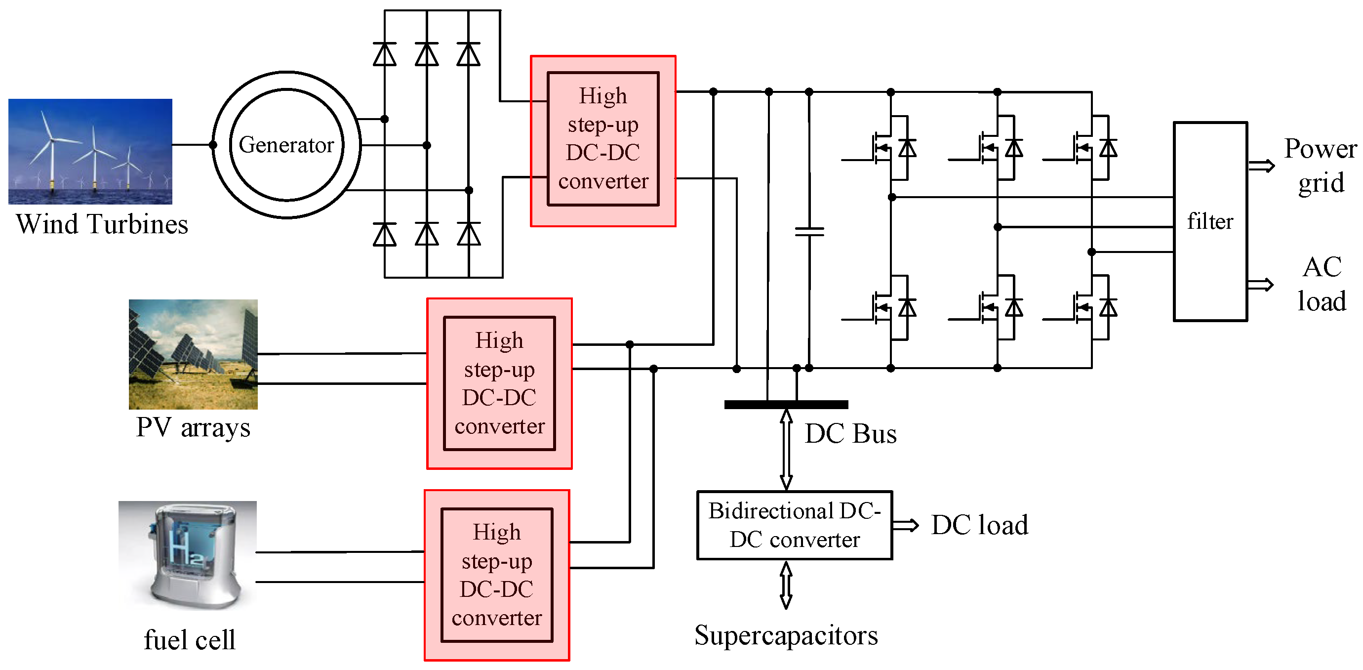
2]. A typical grid-connection renewable energy power generation system is shown in
Figure 1.
In summary, the utilization process of renewable energy requires a high-gain DC-DC booster device to convert the low-voltage output of the renewable device into the inverter side high-voltage output. Theoretically, conventional Boost converters can achieve high voltage gain by increasing the duty cycle. However, in practice, affected by parasitic parameters, it can only achieve 4–6 times voltage gain [
3,
4,
5]. Therefore, the traditional Boost converter needs to be improved and perfected in order to achieve a high-voltage gain DC-DC converter. Common voltage multiplier units feature a two-port structure, where the output voltage at the secondary port is
M times the input voltage at the primary port. The voltage gain
M varies with changes in the topology and the duty cycle of the main circuit’s switching transistor [
6]. Similarly to switch-capacitor boost structures, the presence of zero-state capacitors in the circuit causes significant inrush currents during converter startup [
7]. This paper aims to propose a control method to address inrush currents.
Non-common-ground coupled inductive interleaved Boost converter (NCG-CIIBC) is a high-gain DC-DC converter with non-common-ground input and output [
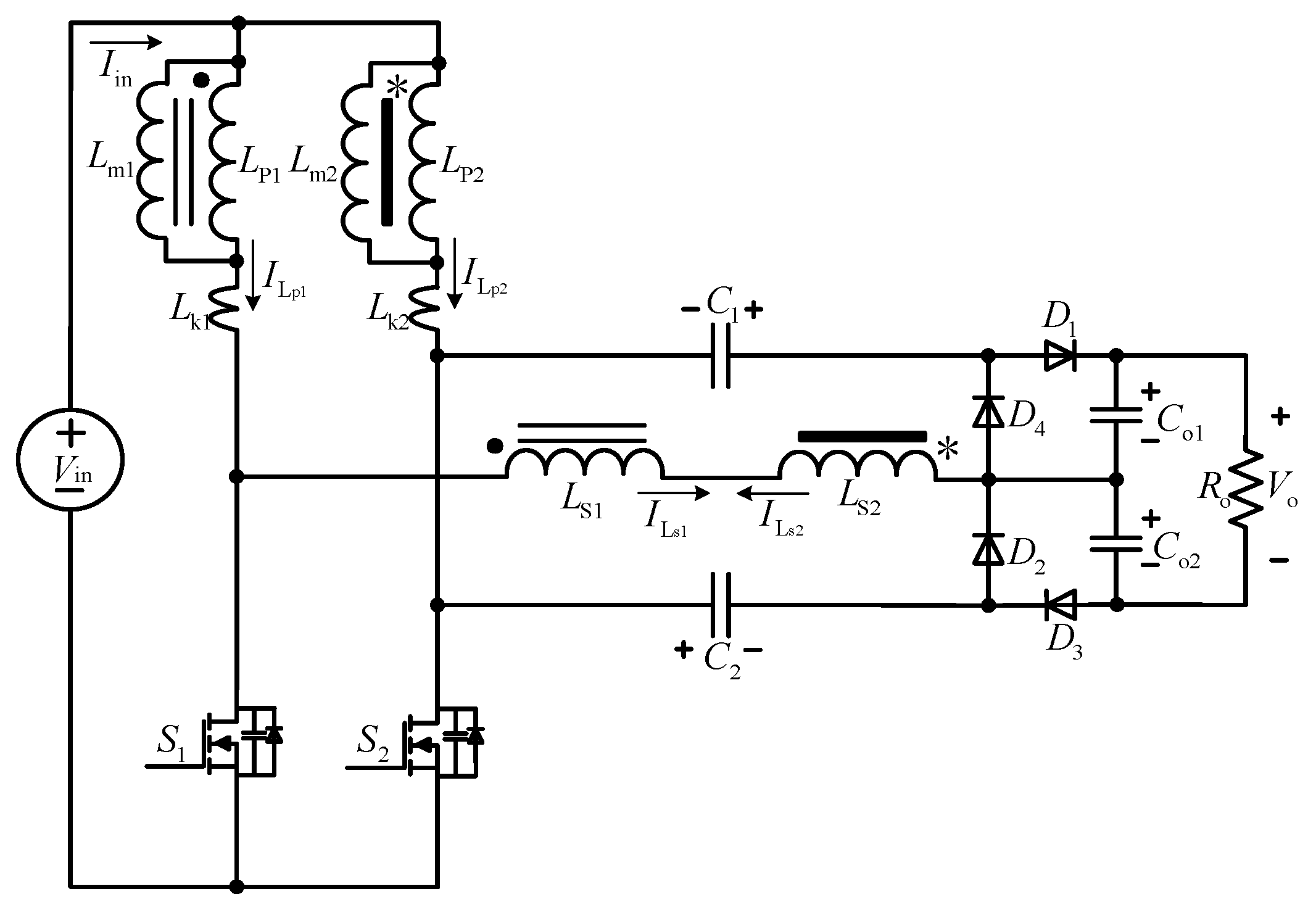
8]. The topology configuration is shown in
Figure 2. It is mainly composed of two MOSFETs, S
1 and S
2, two coupled inductors, L
1 and L
2, two double voltage capacitors, C
1 and C
2, four diodes, D
1–D
4, and two load capacitors, C
o1 and C
o2. Since the coupled inductor shares a similar structure to a transformer, for ease of analysis, the primary side of the coupled inductor is equivalent to the excitation windings
and
, the primary windings and
,
and the leakage inductance
and
.
and
are the secondary windings of the coupling inductor. For simplicity, the coupling inductor is collectively referred to as
L1 and
L2. In the figure, the small star (*) and large dot (•) symbols represent different types of coupled inductors. The small star symbolizes one coupling configuration, while the large dot represents another configuration. These distinctions help to clarify the various magnetic coupling methods used in the circuit.
NCG-CIIBC combines inductor interleaving technology and voltage doubling capacitor boost technology, and replaces the input inductor in the Boost topology with a coupling inductor, improving voltage gain and reducing input current ripple [
9]. However, in order to ensure a continuous path for the input current, the NCG-CIIBC can only operate at a duty ratio
D > 0.5, which limits the operating range of the NCG-CIIBC and restricts topology expansion [
10]. In addition, during dynamic processes such as startup, direct startup with
D > 0.5 will generate large surge input currents, greatly improving the requirements for the current passing ability of switching devices, and hindering the large-scale application of NCG-CIIBC [
11].
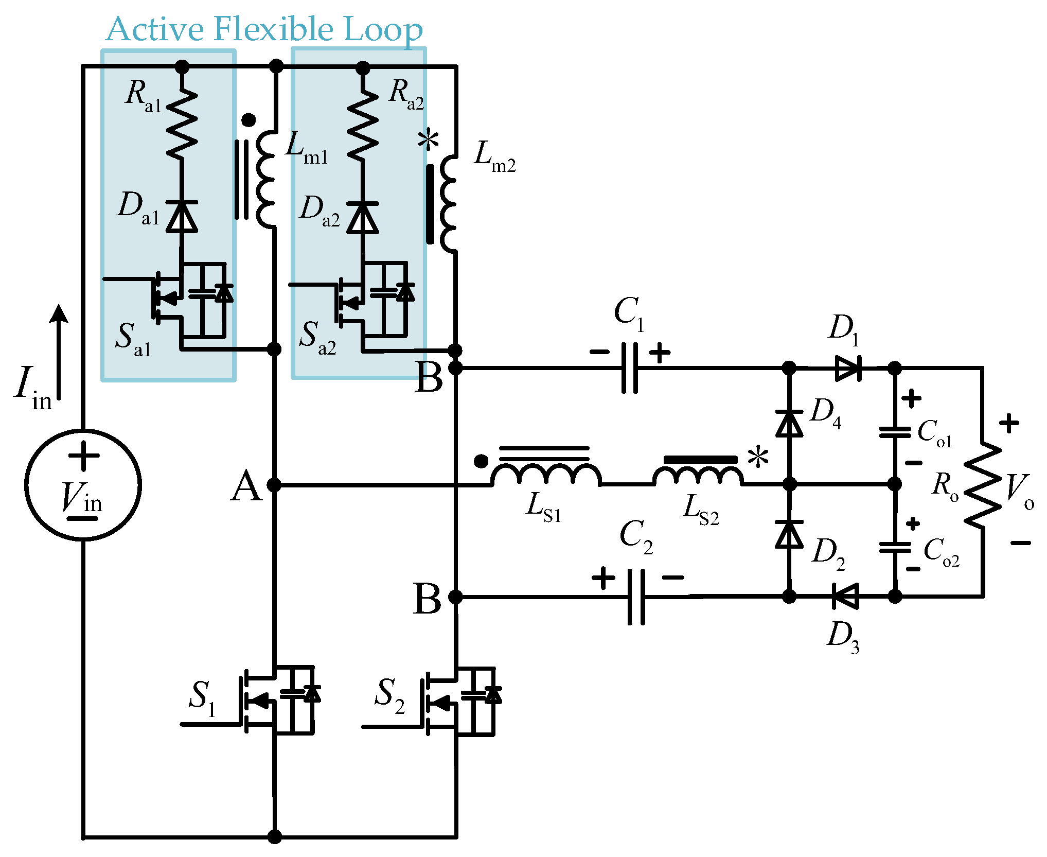
As shown in
Figure 3, this paper designs an active flexible loop (AFL) through topology improvement. The introduction of the active flexible loop (AFL) in the NCG-CIIBC-AFL converter significantly enhances its operational range, enabling stable operation across the full duty cycle range. Traditionally, converters face limitations at lower duty cycles, especially when the duty cycle is below 0.5, where the current path is often interrupted due to the main switches being off. The AFL addresses this challenge by incorporating auxiliary MOSFETs that provide a continuous current path when the main MOSFETs are off. This allows the converter to maintain stable operation even at lower duty cycles, preventing performance degradation and ensuring high voltage gain throughout the entire duty cycle range. As a result, the converter exhibits improved system adaptability, providing efficient power conversion across a wide range of operating conditions, from low to high duty cycles. AFL ensures that the input terminal of the NCG-CIIBC also has a stable current path when the duty ratio
D < 0.5, thereby obtaining the NCG-CIIBC-AFL converter 7.
The active flexible loop (AFL) in the box of
Figure 3 consists of auxiliary MOSFETs
Sa1 and
Sa2, auxiliary diodes
Da1 and
Da2, and energy discharge resistors
Ra1 and
Ra2. The two AFL circuits are connected in parallel to the primary windings of the coupling inductors
L1 and
L2, respectively. The switching logic of the auxiliary MOSFETs
Sa1 and
Sa2 is based on an OR condition with the main MOSFETs
S1 and
S2. When both main MOSFETs are off, the auxiliary MOSFETs
Sa1 and
Sa2 turn on, allowing continuous current flow through the inductor. When either main MOSFET is on, the auxiliary MOSFETs turn off, causing energy storage in the inductor.
In addition, to suppress the input surge current during the startup process of NCG-CIIBC-AFL, this paper proposes a collaborative control strategy of “open loop flexible compensation—closed loop linear compensation”, which fully utilizes the controllability of open-loop control far from the equilibrium point of the system and the robustness of closed-loop control near the stable point of the system, improving the dynamic performance of the system. The ultimate step for improving precision and speed of response is the introduction of closed-loop control [
12]. Finally, an NCG-CIIBC-AFL prototype with a maximum output power of 100 W is built to verify the effectiveness of the proposed NCG-CIIBC-AFL converter and its control strategy.
2. Principal Analysis of NCG-CIIBC-AFL
To simplify the analysis, the following assumptions are made: (1) Power devices are ideal components, that is, the switching on loss, off loss, and on loss of the switch are all zero, ignoring the parasitic resistance of the inductor and capacitor, and ignoring the on loss of the diode. (2) The parameters of coupling inductance L1 and L2 are consistent; the coupling degree of the coupling inductance is large enough; the inductance of the coupling inductor is large enough to ignore the effect of magnetic circuit saturation; the capacity of the capacitor is large enough.
2.1. Modal Analysis Under Operating Conditions with Duty Ratio D > 0.5
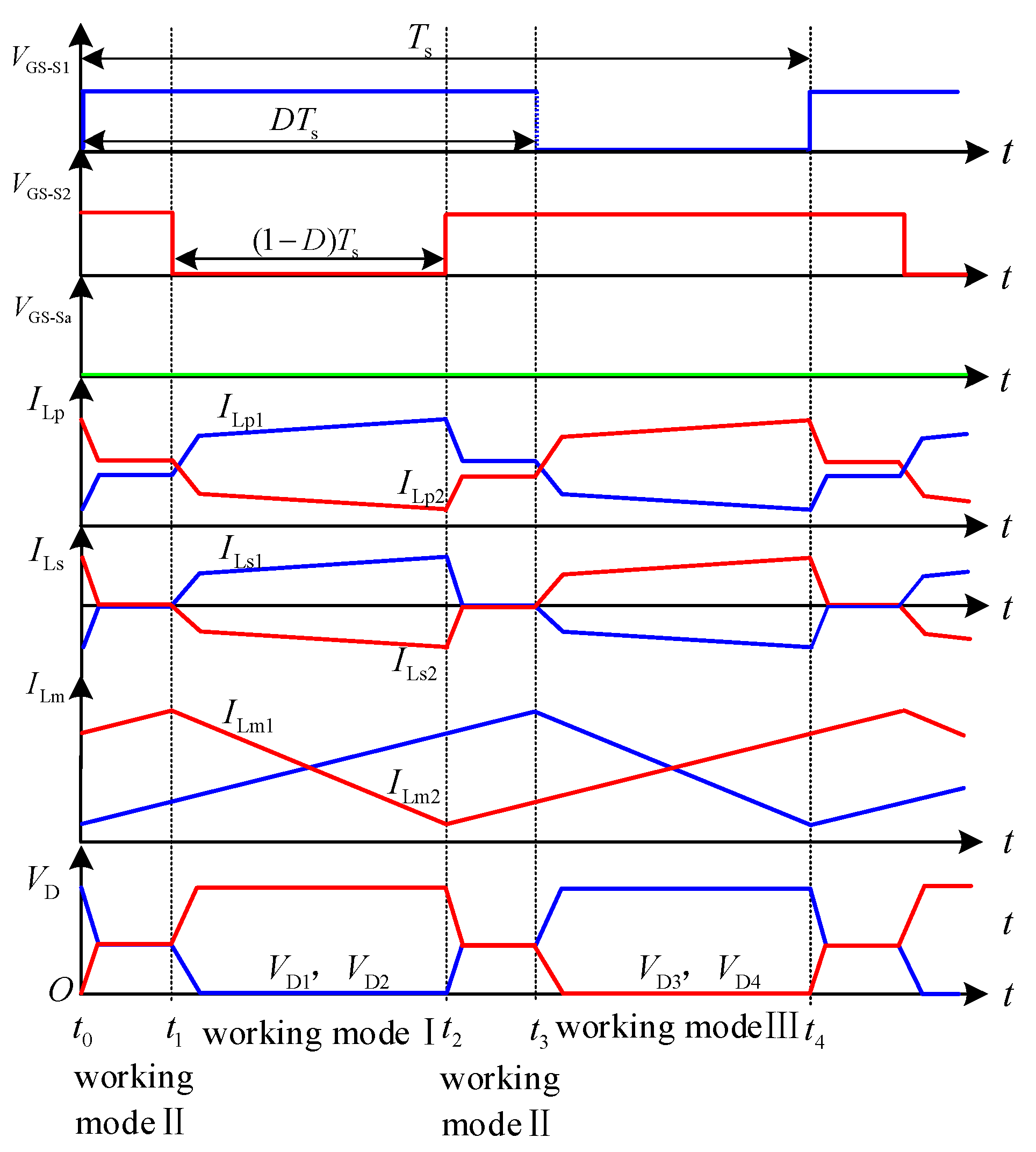
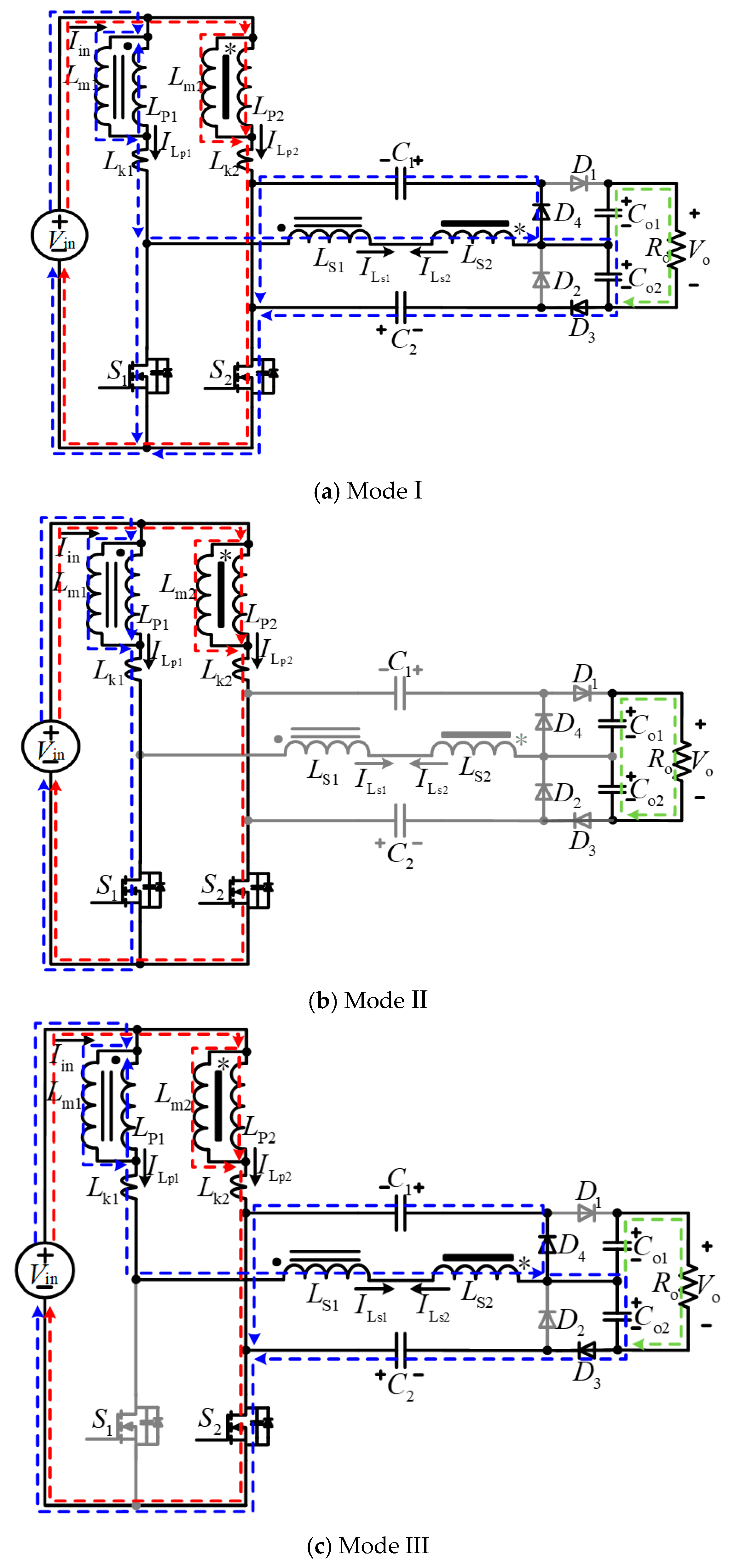
NCG-CIIBC-AFL has three stable modes in a switching cycle under the operating mode with a duty ratio
D > 0.5. The key waveform is shown in
Figure 4, and the operating state of each mode is shown in
Figure 5.
In the working mode I, the following equation holds:
In working mode II, the following equation holds:
In working mode III, the following equation holds:
From Equations (2) and (7), the following can be obtained:
From Equations (1), (4)–(6), the following can be obtained:
From the equivalent excitation inductance, the volt-second balance principle of the coupling inductance, the following conclusion can be made:
Bringing Equations (9) and (10) into Equations (11) and (12) yields
By introducing Equations (13) and (14) into Equations (3) and (8), respectively, the following can be obtained:
On the output side, there are
By bringing Equation (15) into Equation (16), the following can be obtained:
where
N is the ratio of turns of the primary and secondary sides of the coupling inductor, and
k is the coupling coefficient of the primary and secondary sides.
According to Equation (17), the steady-state voltage gain of the NCG-CIIBC-AFL converter at a duty ratio
D > 0.5 can be obtained:
From the above formula, it can be seen that steady-state voltage gain is related to duty ratio D, turn ratio N, and coupling coefficient k.
2.2. Modal Analysis Under Operating Conditions with Duty Ratio D < 0.5
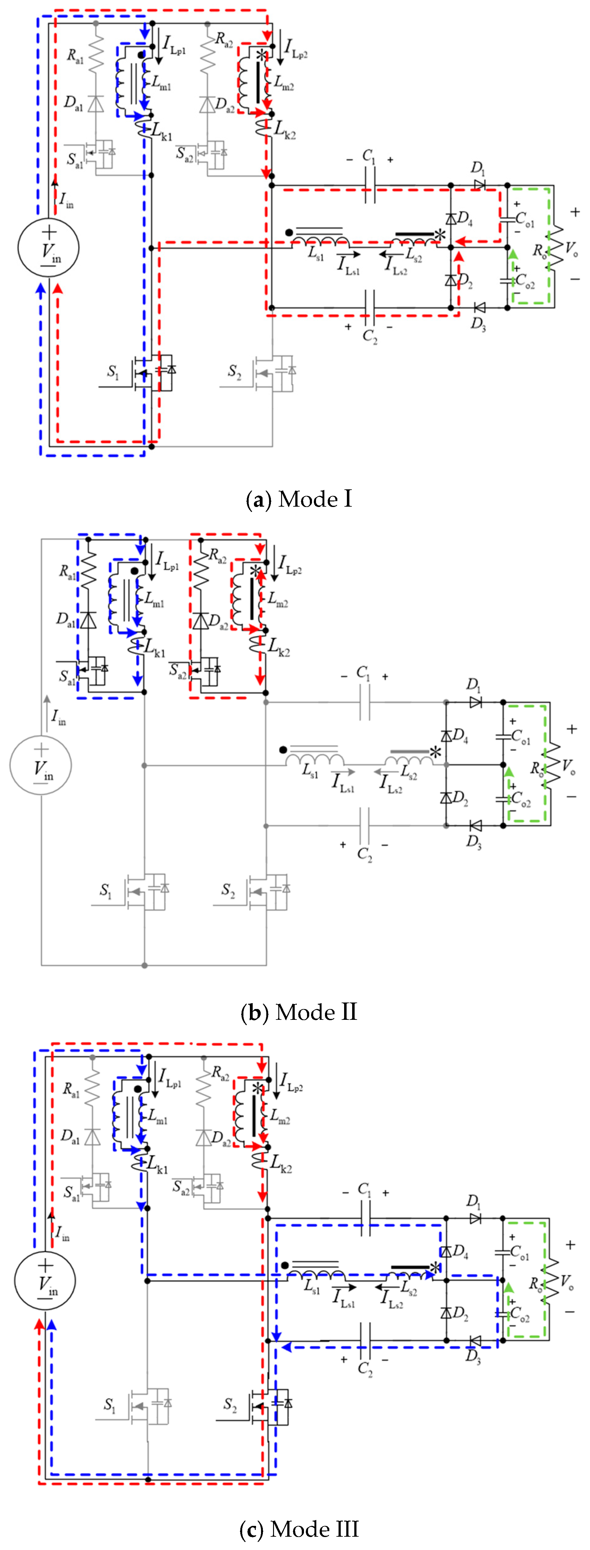
NCG-CIIBC-AFL also has three stable modes in a switching cycle under the duty ratio
D < 0.5 operating mode. The key waveform is shown in
Figure 6, and the operating state of each mode is shown in
Figure 7.
In the working mode I, the following equation holds:
In working mode II, the following equation holds:
In working mode III, the following equation holds:
From Equations (19), (22) and (25), it can be obtained that the voltage of the coupling inductor
in a switching cycle is
From Equations (20), (23) and (24), it can be obtained that the voltage of the coupling inductor
in a switching cycle is
According to the volt-second balance principle of the equivalent excitation inductances
and
of the coupling inductance, the following conclusion can be made:
Substituting Equation (27) into Equation (29) and bringing Equation (28) into Equation (30) yields
is the AFL circuit discharge time constant.
According to Equation (32), the voltage gain
of NCG-CIIBC-AFL under operating conditions
D < 0.5 is
From Equation (33), it can be seen that the voltage gain of NCG-CIIBC-AFL at a duty ratio D < 0.5 is not only related to the duty ratio D, the coupling inductance turn ratio N, and the coupling coefficient k, but also related to parameters such as the discharge time constant and the switching cycle of the AFL circuit.
By combining Equation (18) and Equation (33), the voltage gain
M of NCG-CIIBC-AFL in the full duty cycle range can be obtained:
Select the coupling inductance turn ratio
N = 1 and the coupling coefficient
k = 0.98, select the switching cycle
as
s, and the value of the time constant
should be as close as possible to
, select
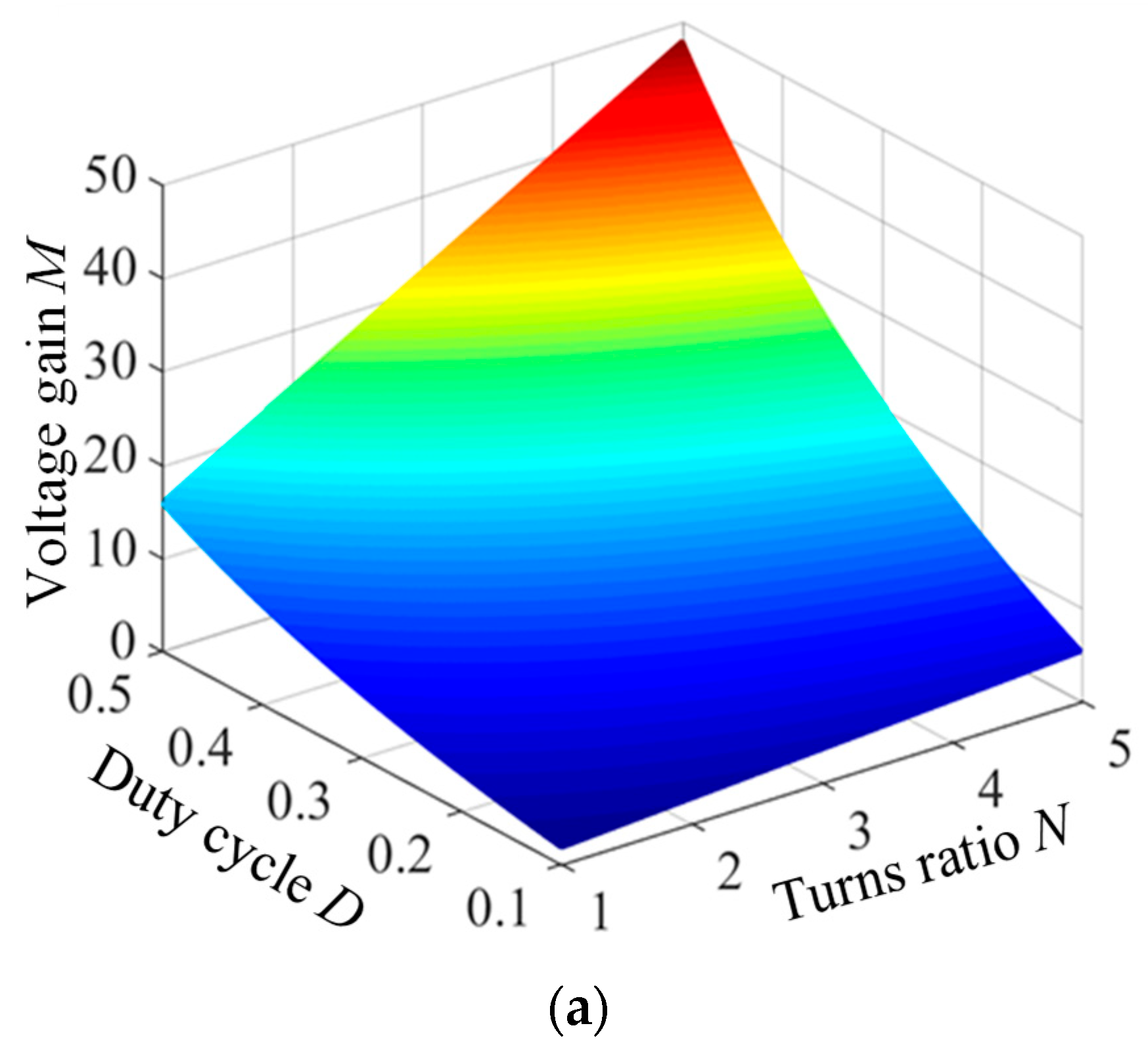
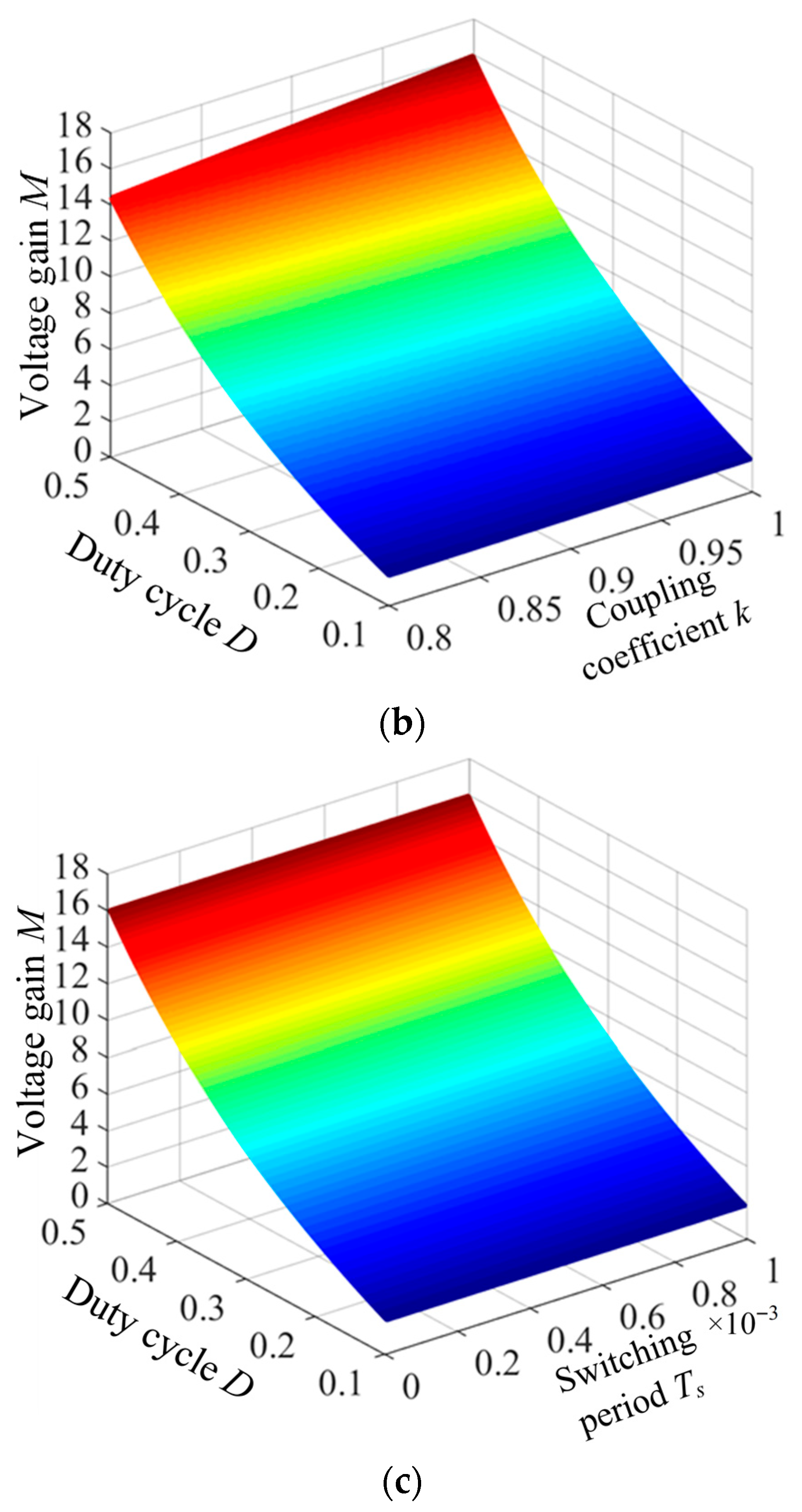
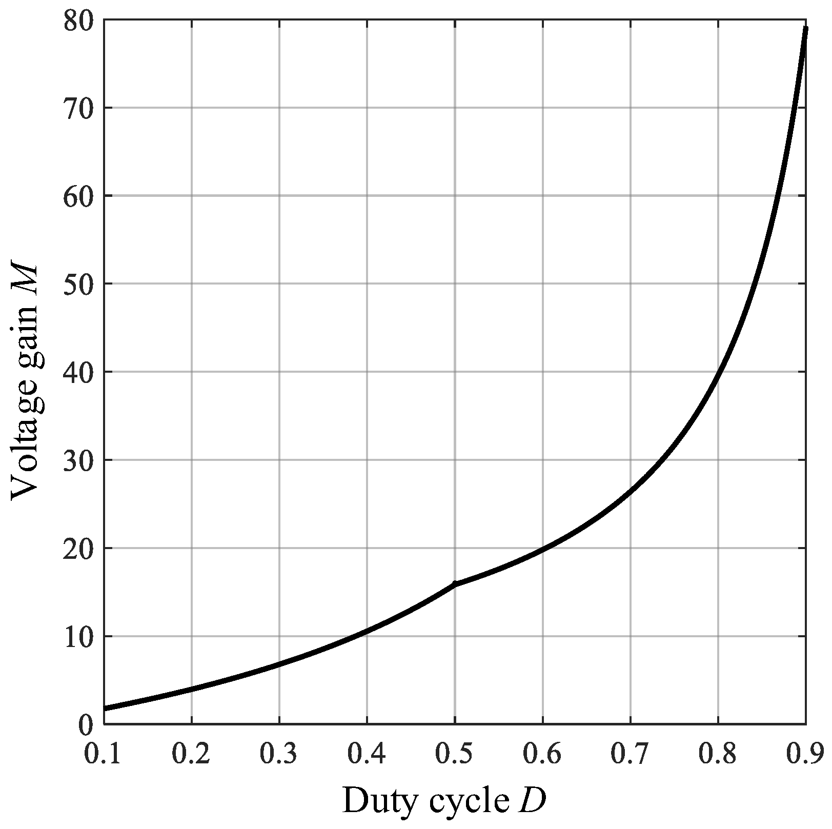
s. According to Equation (34), the voltage gain curves of the NCG-CIIBC-AFL at duty cycles
D < 0.5 and across the entire duty cycle range can be obtained, as shown in
Figure 8 and
Figure 9.
The addition of an AFL expands the operational form of the converter. In theory, NCG-CIIBC-AFL can achieve voltage gain from zero to any multiple. Therefore, NCG-CIIBC-AFL has a richer working mode and higher adaptability to duty ratio, which can achieve a duty ratio starting from zero, providing a topological basis for solving the problem of NCG-CIIBC-AFL starting surge current.
3. Cooperative Control Design of Open-Loop Flexible Compensation-Closed-Loop Linear Compensation
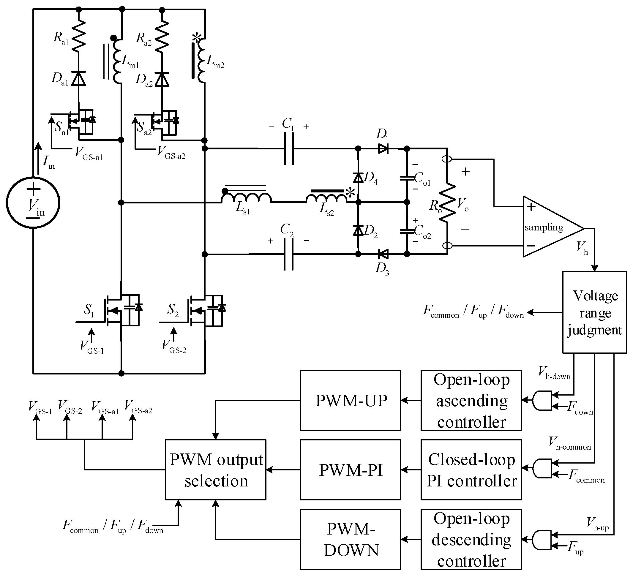
In order to fully utilize the controllability of open-loop control far from the equilibrium point of the system and the robustness of closed-loop control near the stable point of the system, a collaborative control strategy of “open loop flexible compensation—closed loop linear compensation” is designed, and its control block diagram is shown in
Figure 10.
The control idea of the open-loop–closed-loop cooperative control strategy is to set the upper limit threshold value and the lower limit threshold value for the output voltage , and select different control methods by judging the relationship between the output voltage and the upper and lower threshold values.
In
Figure 9, the voltage range determination module is used to determine and compare the output voltage range at the current time and apply corresponding control methods. The upper threshold voltage
and lower threshold voltage
used for comparison are selected based on 5% of the reference voltage
, namely
when the actual output voltage
is divided by the voltage divider network and the collected voltage
is between
and
, the voltage range determination module outputs a
signal and activates the voltage closed-loop PI controller; when the collected voltage
is greater than
, the voltage range determination module outputs an
signal and activates the open loop descent controller to perform open loop descent control; when the collected voltage
is less than
, the voltage range determination module outputs a
signal and activates the open loop rise controller to perform open loop rise control.
Closed-loop linear PI compensation is a commonly used linear compensation method when a system works near a stable equilibrium point. By modeling the small signal of NCG-CIIBC-AFL and designing the compensation network, it can be obtained that the open loop transfer functions
,
, and the transfer function
of the compensation network for NCG-CIIBC-AFL under duty ratios
D > 0.5 and
D < 0.5 are
The expressions for num, den,
, and
are shown in the
Appendix A.
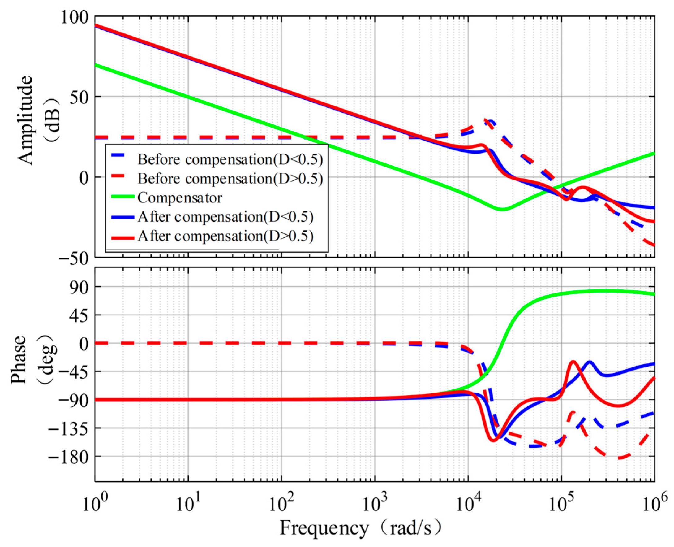
The NCG-CIIBC-AFL open-loop Bode diagram before and after compensation is shown in
Figure 11. As can be seen from
Figure 10, after adding compensation link correction, the phase margins of NCG-CIIBC-AFL under operating conditions with duty ratios
D > 0.5 and
D < 0.5 are 55.3° and 63.3°, respectively, and the cutoff frequencies are 28.1 kHz and 30.0 kHz, respectively. The low-frequency system gain is significantly improved, while the high-frequency system gain rapidly decreases, improving system stability and reducing high-frequency noise interference.
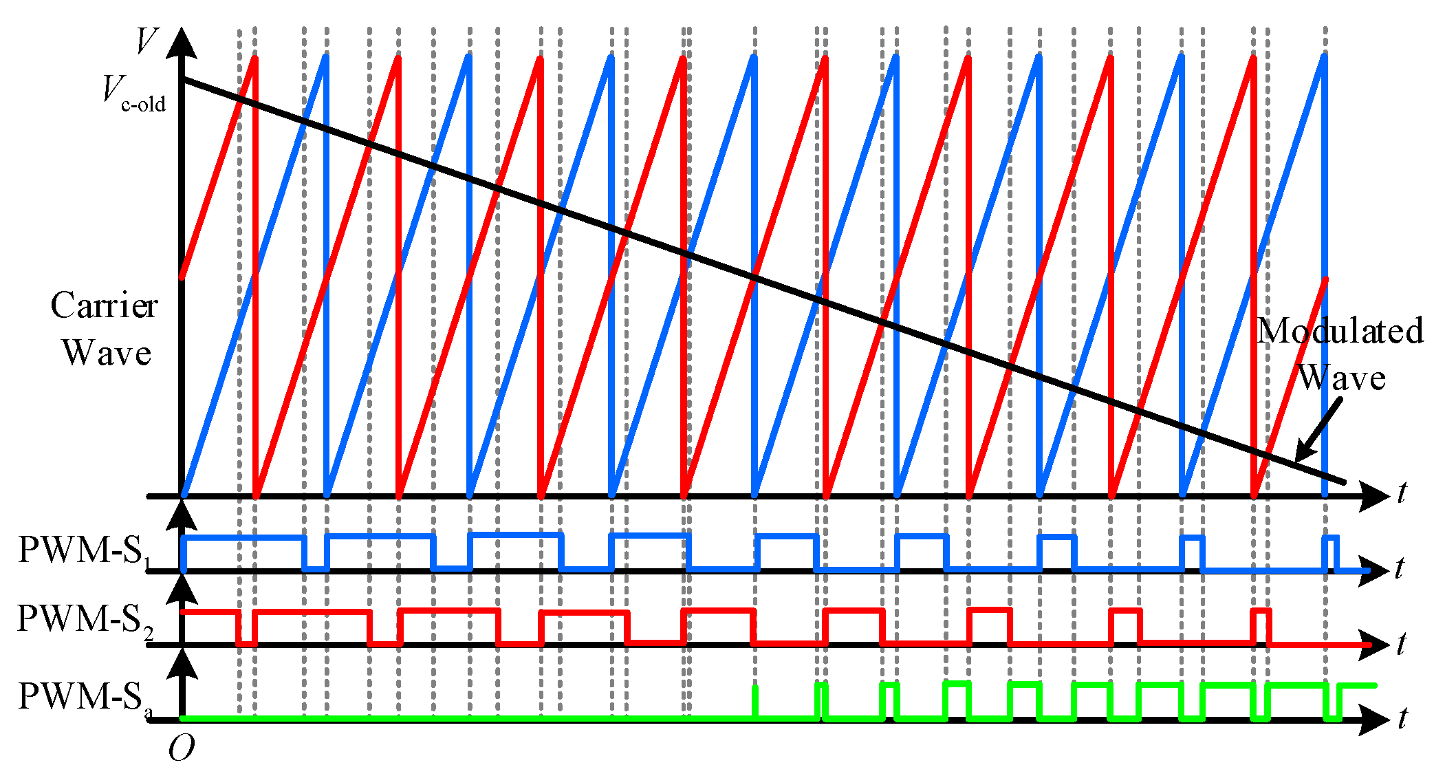
The open-loop descent control strategy is shown in
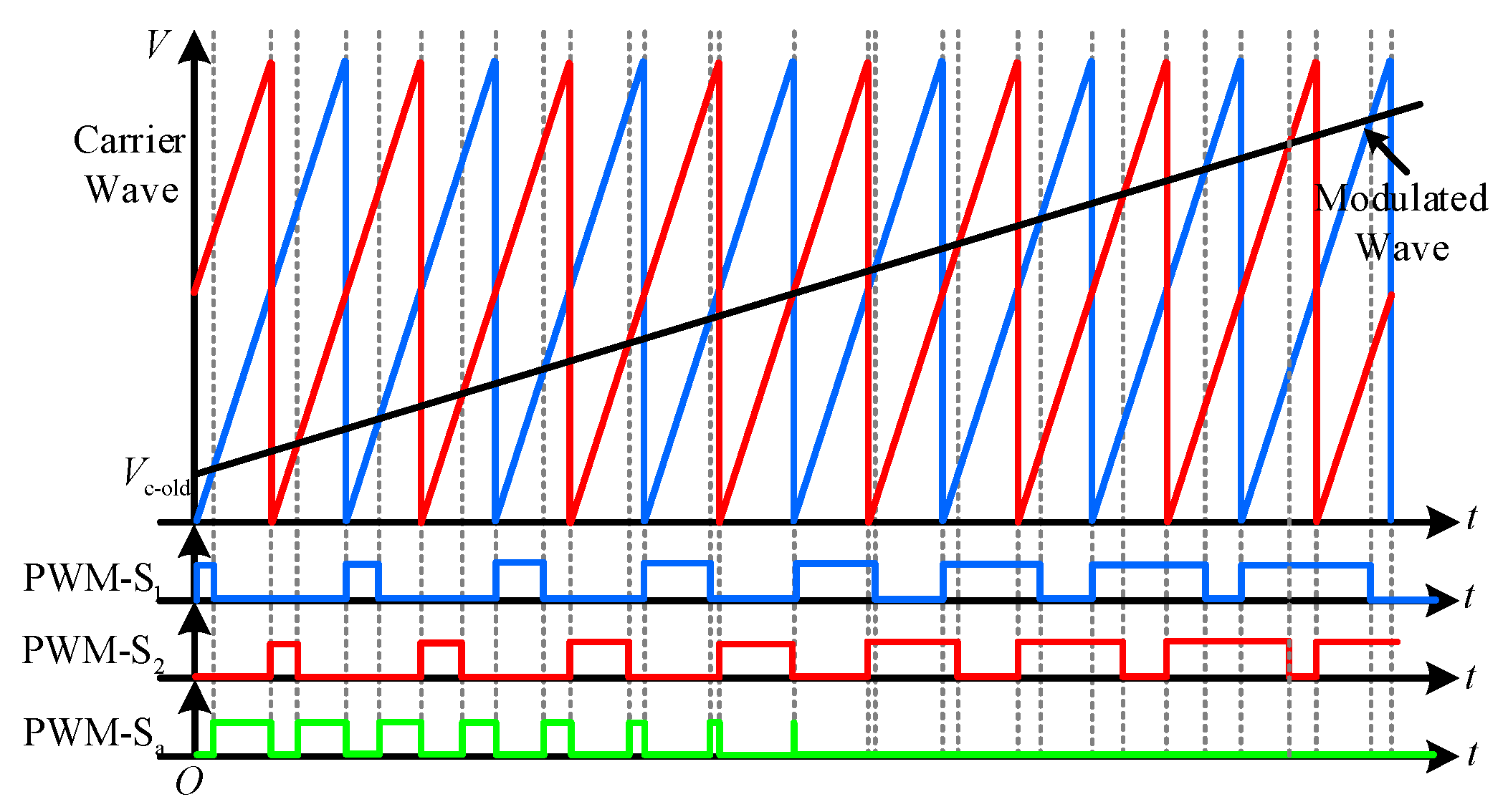
Figure 12. The modulation wave voltage value
at the end of the previous control cycle of the open-loop descent controller is used as the starting operating point, and the duty cycle is linearly reduced according to the set descent slope. During 100 switching cycles, the modulation voltage
linearly decreases by 1%, that is, the duty ratios of the main MOSFETs
S1 and
S2 linearly decrease by 1%, and the duty ratios of the auxiliary MOSFETs
Sa1 and
Sa2 linearly increase by 2% (if any). The modulation wave expression in the open-loop descent control mode is
The open-loop rise control strategy is shown in
Figure 13. The operating principle of the open-loop up controller and the open-loop down controller is the same, but the modulation voltage
changes in the opposite direction.
The PWM output selection controller mainly has two functions. One is to select the source of the output PWM signal by receiving the voltage range signal provided by the output voltage range detection module and outputting it to the drive circuit. Another function is to save the PWM information of the last switching cycle in each control cycle as a PWM-old signal. Through the PWM-old signal, the initial modulation voltage for the next control mode can be obtained and provided to the open-loop up controller and open-loop down controller to determine the initial duty ratio of each MOSFET.
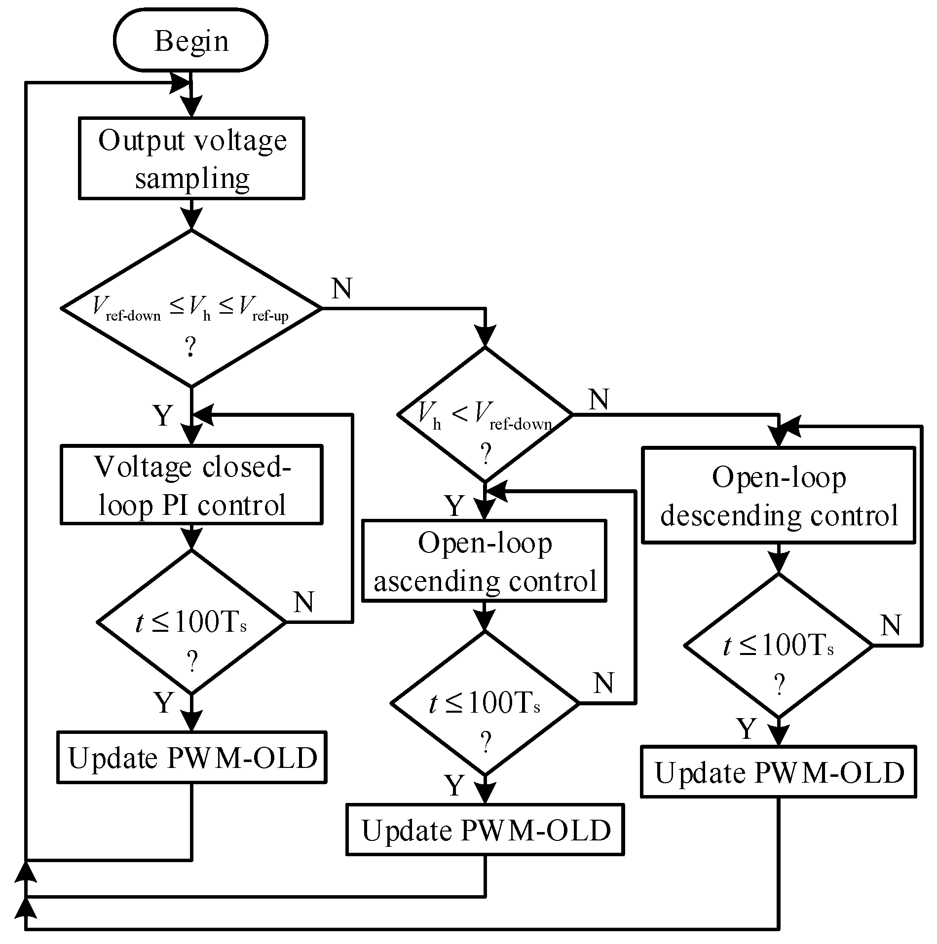
The flow chart of the open-loop–closed-loop cooperative control strategy is shown in
Figure 14.
The workflow of the open-loop–closed-loop collaborative control strategy can be described in detail as follows:
- (1)
Every 100 switching cycles, the voltage range determination module judges the magnitude relationship between the collected voltage from the voltage divider network, the upper threshold voltage , and the lower threshold voltage
- (2)
If the collected voltage is between and , the voltage range determination module outputs a signal, and the system enters a voltage closed-loop linear PI control mode. The PI controller operates and outputs a PWM-PI signal.
- (3)
When the collected voltage is outside of and , further compare the size relationship between and , and to determine the open loop operating mode of the system. If the collected voltage is less than , the voltage range determination module outputs a signal, and the system enters the open loop rise control mode. The open-loop rise controller starts and outputs a PWM-UP signal. If the collected voltage is greater than , the voltage range determination module outputs a signal, and the system enters the open loop down control mode. The open-loop down controller starts and outputs a PWM-DOWN signal.
- (4)
Once the system enters a certain control mode, the system will be locked in this mode for the next 100 switching cycles. The PWM output controller selects the corresponding controller’s PWM signal output based on the voltage range judgment module’s output signal. When a control cycle ends, the PWM output controller stores the PWM output signal of the last switching cycle of the control mode as PWM-OLD, providing an initial duty cycle for the next control mode.
- (5)
After the end of a control cycle, the output voltage range judgment module starts again, and the system enters a new control mode.
4. Experiment
An experimental prototype of the NCG-CIIBC-AFL converter with a maximum output power of 100 W has been built at the Power Electronics and Power Drives Laboratory, Harbin Institute of Technology, Shenzhen Campus, Guangdong Province, China. The main component parameters are shown in
Table 1.
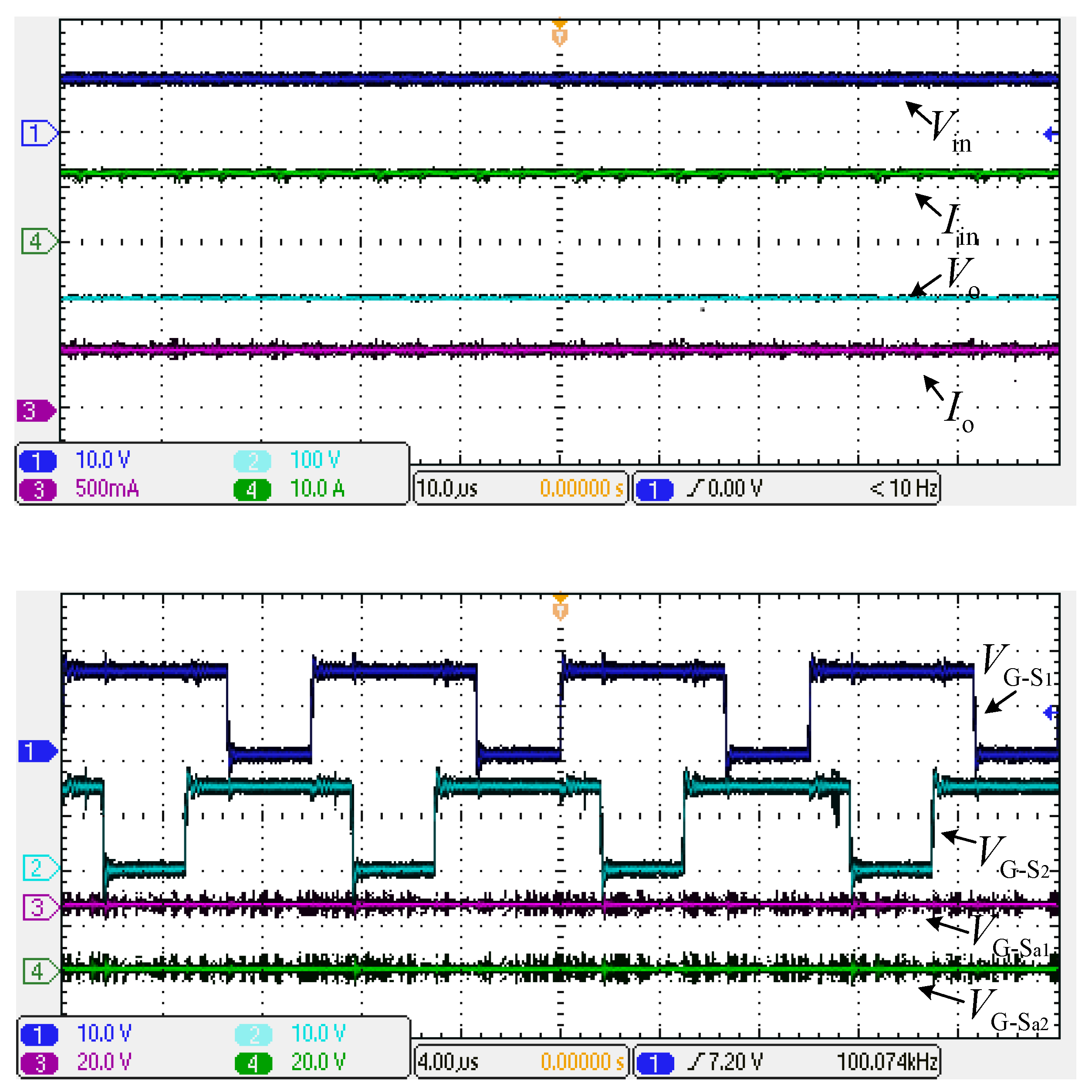
The steady-state experimental results of the NCG-CIIBC-AFL prototype operating at 20 times the voltage gain are shown in
Figure 15. The duty ratio
D is 0.6, the input voltage
is 10 V, the input current
is 11.3 A, the output voltage
is 200 V, and the output current
is 500 mA. The input current AC ripple
is 500 mA, with a ripple rate of 4.42%; The output voltage
has an AC ripple of 3 V, with a ripple rate of 1.5%. The main MOSFETs
S1 and
S2 are staggered for 180° conduction at a frequency of 100 kHz; The driving signals of the auxiliary MOSFETs
Sa1 and
Sa2 are always zero.
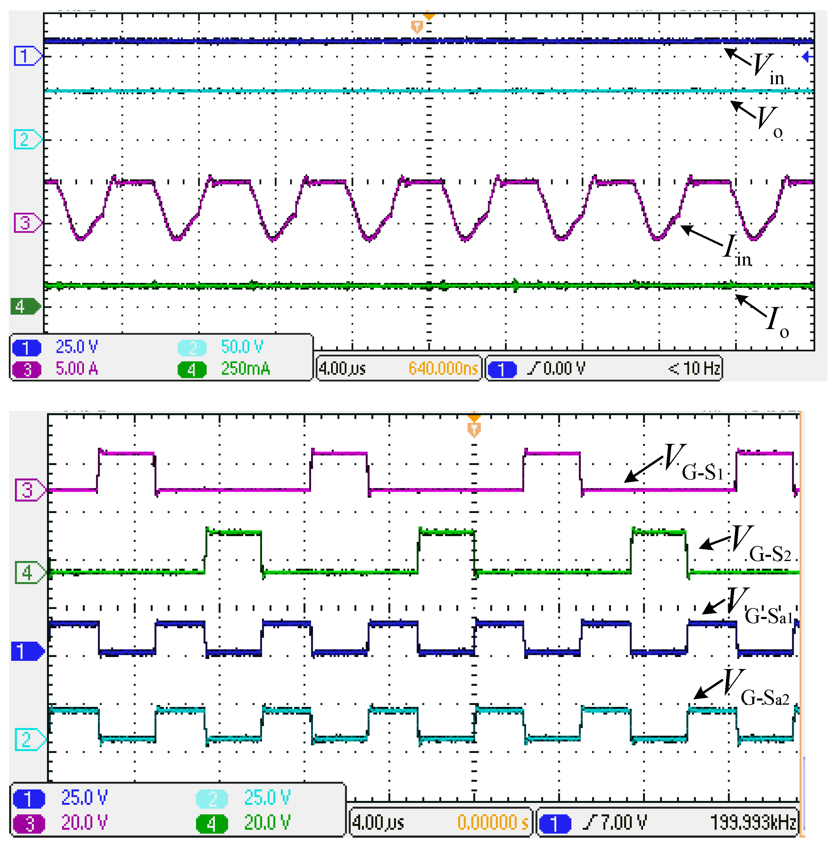
The steady-state experimental results of the NCG-CIIBC-AFL prototype operating at 6 times the voltage gain are shown in
Figure 16. The duty ratio
D is 0.28, the input voltage
is 10 V, and the input current
is intermittent, with a maximum value of about 5 A. The output voltage
is 60 V, and the output current
is 150 mA. The duty cycle of the driving signal of the main MOSFETs
S1 and
S2 is 0.28, the phase difference is 180°, and the frequency is 100 kHz; the drive signal duty ratio of the auxiliary MOSFETs
Sa1 and
Sa2 is 0.44, and the frequency is 200 kHz.
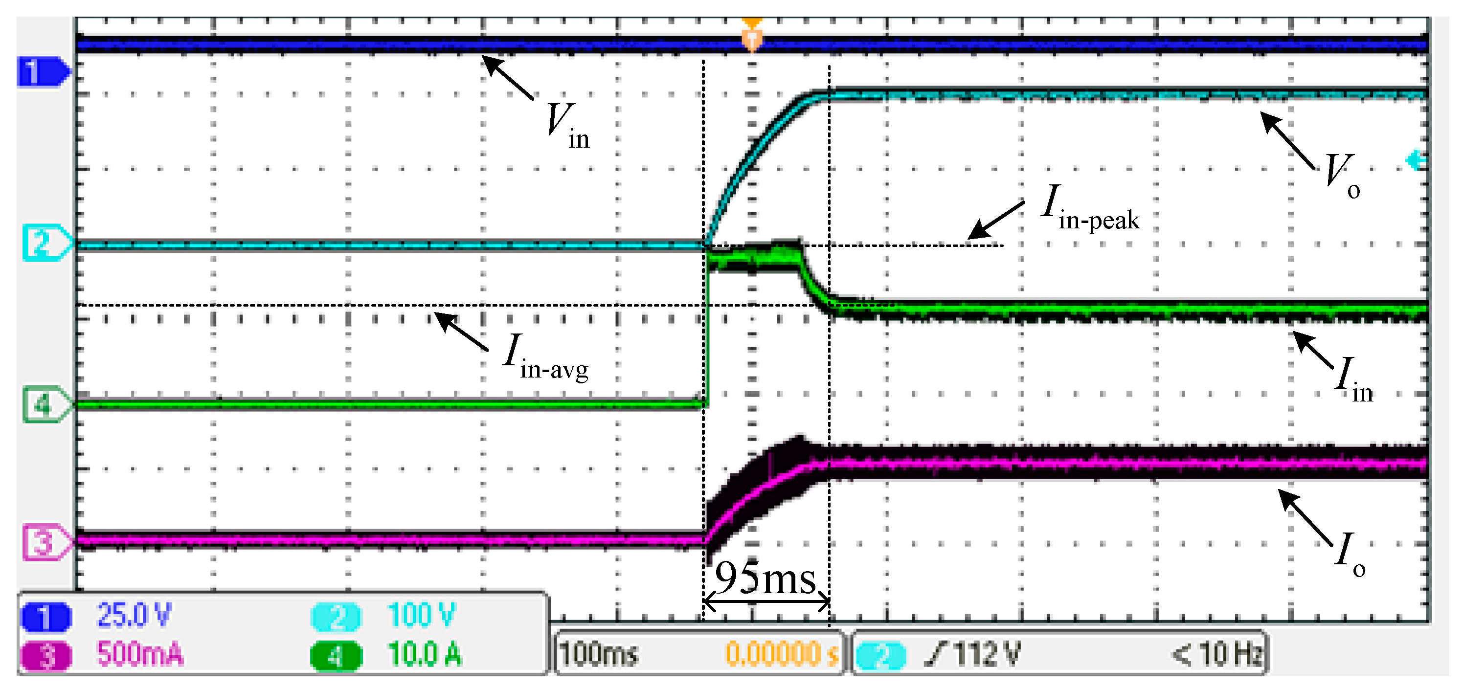
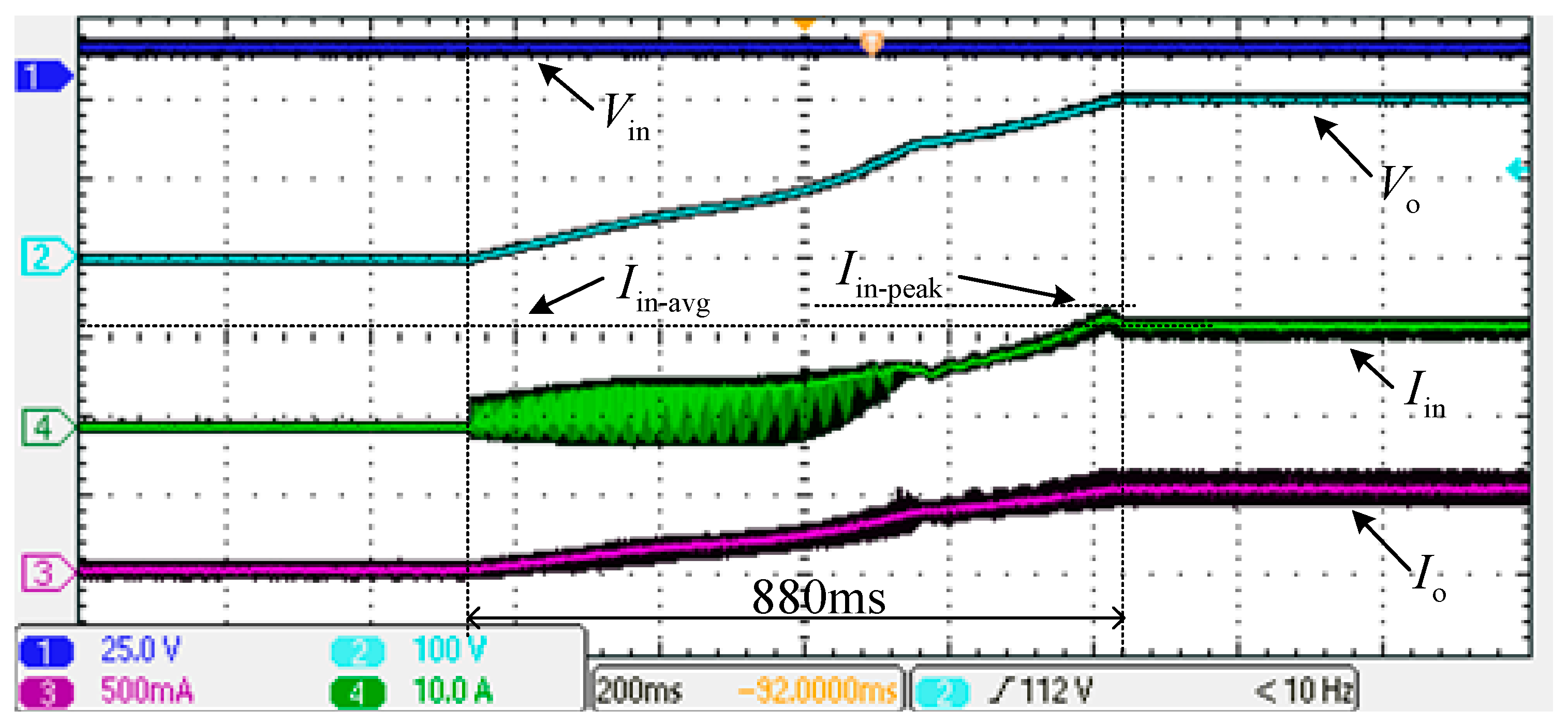
The startup waveform of the NCG-CIIBC-AFL prototype is shown in
Figure 17 and
Figure 18.
Figure 17 shows the startup waveform using only traditional voltage closed-loop PI control. Due to hardware constraints, the maximum rated output current of the power supply is 20 A. At the moment of startup, the input current
reaches the maximum power output value of 20 A, and then slowly drops to a steady-state value of 11.3 A.
Figure 18 shows a waveform initiated using an open-loop–closed-loop cooperative control strategy. The output voltage
is 200 V, and there is no overshoot. The input current
is 11.3 A, the input current peak
is about 12.2 A, and the overshoot rate is only 7.9%.
5. Conclusions
This paper proposes a coupled inductor type interleaved boost converter with an active flexible circuit. The converter utilizes an interleaved connection, two coupled inductors, and a voltage-doubling capacitor boost link to achieve high voltage gain and low input current ripple. The active flexible circuit expands the working range of the converter and expands the application of this topology. In addition, a collaborative control strategy of open-loop flexible compensation and closed-loop linear compensation is proposed to effectively limit the input surge current. A hardware experimental platform has been built to prove the correctness of the proposed converter and control method. To compare the steady-state performance of the NCG-CIIBC, converters proposed in references [
13,
14,
15,
16,
17] were selected for comparison under conditions of primary-to-secondary turn ratio N = 1 and coupling coefficient k = 0.95. Key performance metrics are summarized in
Table 2, which outlines the steady-state performance indicators for each converter. Under identical duty cycles, the NCG-CIIBC consistently achieves higher voltage gain than the converters in [
13,
14,
15,
16,
17,
18,
19], while simultaneously reducing voltage stress on switching devices. The maximum voltage stress on the diodes in the NCG-CIIBC is lower than that in the converters of [
15,
16,
17], equivalent to that in [
14], and higher than that in the converter proposed in [
13]. Regarding cost, the number of diodes and capacitors used in [
16,
17] is lower than that of the NCG-CIIBC, while the number of major components used in [
13,
14,
15] is higher than that of the NCG-CIIBC. Considering the above performance metrics, the NCG-CIIBC achieves higher voltage gain without increasing system cost. Reference [
19] realizes soft switching (ZVS), significantly reducing switching losses, but sacrifices voltage gain, making it less suitable for high step-up applications. Reference [
18], although offering higher voltage gain, suffers from increased switching stress, leading to higher losses. In contrast, the NCG-CIIBC offers a high voltage gain with balanced switching stress and minimal losses, achieving superior performance without increasing system cost.
