Article

Conducted Common-Mode Electromagnetic Interference Analysis of Gate Drivers for High-Voltage SiC Devices

by
Kai Xiao
1,
Haibo Tang
2,
Zhihong Cai
1,
Yansheng Zou
1 and
Jianyu Pan
2,*
1
CSG EHV Electric Power, Research Institute, China Southern Power Grid Company Limited, Guangzhou 510663, China
2
State Key Laboratory of Power Transmission Equipment Technology, Chongqing University, Chongqing 400044, China
*
Author to whom correspondence should be addressed.
Energies 2025, 18(23), 6083; https://doi.org/10.3390/en18236083
Submission received: 25 June 2025 / Revised: 5 August 2025 / Accepted: 7 August 2025 / Published: 21 November 2025

Abstract

Power conversion equipment based on high-voltage SiC devices offers significant advantages in efficiency and power density. However, during high-voltage, high-power switching operations, severe electromagnetic interference (EMI) can easily occur. It could cause the false triggering of devices and result in converter failure in severe conditions. This paper firstly establishes a mathematical model and conducts simulation analysis of the conducted common-mode interference path in high-voltage SiC device gate driver circuits. Based on the driver circuit architecture, a modeling method for the common-mode interference conduction network in half-bridge submodules is proposed, clarifying the key factors contributing to high common-mode currents. A low common-mode current design methodology for high-voltage SiC submodules is presented, including driver loop structure optimization, capacitor design, and submodule integration. A highly integrated 3.3 kV SiC-based submodule prototype has been successfully developed, serving as a building block for constructing multilevel modular converters (MMCs). Simulation and experimental results indicate that the amplitude of the common-mode current is primarily influenced by the coupling capacitance of the auxiliary power supply, exhibiting a proportional relationship. The developed SiC submodule achieves high-speed switching at 50 kV/μs under a 2 kV DC bus voltage, with excellent thermal stability and low common-mode current characteristics, validating the effectiveness of the proposed model and design approach.

1. Introduction

Silicon carbide (SiC) devices, owing to their wide bandgap, high switching frequency, and exceptional breakdown electric field strength, have been extensively adopted in applications such as electric vehicles, photovoltaic energy storage systems, and rail transportation [1,2,3]. These devices play a pivotal role in significantly improving the efficiency and power density of power conversion systems [4,5]. Currently, the application of SiC devices across various sectors of the power industry is accelerating. SiC devices with voltage ratings of 1.7 kV and 3.3 kV have been commercialized, while Cree [6] and some universities [7] have developed SiC devices with voltage ratings as high as 10 kV. Studies have shown that using medium-voltage SiC devices rated at 3.3 kV or higher, in combination with two-level or three-level topologies, can elevate the voltage rating of power conversion systems to above 5 kV.
In [8], a three-level ANPC prototype was built using 3.3 kV SiC devices and IGBTs, achieving a DC bus voltage of 4 kV, output power of 40 kVA, and an efficiency of 98.97%. Each single-phase unit weighs 10.4 kg with a volume of 24 L, resulting in a power density of 3.85 kVA/kg and 1.67 kVA/L. In [9], a series resonant converter based on 3.3 kV SiC devices was developed, achieving a voltage rating of 3 kV, power of 25 kW, and an output efficiency of 99.08%. Furthermore, in [10], a half-bridge submodule designed with 10 kV SiC MOSFETs achieved a DC bus voltage of 6 kV, output current of 84 A, operating frequency of 10 kHz, efficiency of 99.3%, and power density of 11.9 kW/L. Existing research demonstrates that power conversion systems based on medium-voltage SiC devices exhibit significant competitive advantages in terms of efficiency, power density, and voltage ratings.
During the switching action of high-voltage SiC devices, a high dv/dt of 10–200 V/ns is generated, which is nearly ten times that of Si devices [11,12,13]. This can cause a high common-mode current to flow back into the weak control circuit, affecting the reliability of the driver. This presents higher EMI interference resistance requirements for the drive circuits of high-voltage SiC devices [14,15]. At present, the main approaches to mitigating electromagnetic interference (EMI) in wide bandgap (WBG) semiconductor gate drivers include the following: the use of common-mode chokes [16], shielding techniques [17], and the reduction of the coupling capacitance in isolated power supplies to suppress overall common-mode currents [18,19,20]. There is limited research on the common-mode interference coupling paths, and no studies have analyzed the multiple propagation paths formed by signal and power branches in the drive circuit, nor have they examined the impedance characteristics of the components in each branch. Due to the flaws in the construction of the propagation network, designers are unable to determine the common-mode interference current at sensitive nodes accurately.
This paper investigates the common-mode conduction interference in a half-bridge submodule based on high-voltage SiC MOSFETs. First, an impedance model of the common-mode interference current conduction loop is established, and the amplitude characteristics of the common-mode interference current are analyzed through mathematical derivation. Next, parasitic parameters of the circuit are extracted using Q3D 2024, and an LTspice simulation model is built to evaluate the main factors influencing the amplitude of the common-mode interference current. Based on this, the design and selection of a gate driver circuit with high dv/dt resistance are discussed. A 3.3 kV SiC MOSFET is used to construct the half-bridge submodule, and the electrical performance of the module is verified through double-pulse and buck tests. Finally, the common-mode interference current waveform is measured to validate the accuracy of the established common-mode current model.

2. Analysis of Common Current for Gate Driver

Figure 1 illustrates the complete structure of the gate drivers for a half-bridge submodule. The power ground serves as the reference potential point for the half-bridge circuit and is also the negative terminal of the bus capacitor. The weak ground acts as the reference potential for the power supply cabinet, with the auxiliary power drawn from this point to supply the driver board. The reference ground on the isolated side of the high-side driver board is connected to the source of switch Q1 (the switching node of the half-bridge circuit, SW), thereby driving the switching of Q1. Meanwhile, the reference ground on the isolated side of the low-side driver board is connected to the source of switch Q2 (power ground). Consequently, during the switching process, the high-side driver board primarily withstands the high potential. This section will analyze and model the various branches of the driver circuit in order to solve the coupling characteristics between common-mode currents and interference voltages.

2.1. Modeling of Conduction Electromagnetic Interference in Gate Driver

The source of electromagnetic interference is primarily the switching actions of the power devices Q1 and Q2. Therefore, the half-bridge structure formed by Q1 and Q2 can be equivalently represented as an interference source, Ucm, connected between the half-bridge midpoint and the power ground. A common-mode impedance model characterizes the driver board. From the connection relationships between the weak ground, power ground, and switching nodes in Figure 1, the port model of the common-mode current-conduction path can be derived, as shown in Figure 2. In this model, ZH and ZL represent the common-mode impedance of the high-side and low-side driver boards, respectively. Since the high-side and low-side boards are identical, their common-mode impedances are equal. As shown in Figure 2, the interference current flows from the high-side board into the low-side board and then returns to the ground plane. Within the boards, the interference current is represented as common-mode.
Taking the high-side driver board as an example, this paper further investigates the propagation characteristics of common-mode interference currents in an individual drive circuit, where in addition to requiring isolation capability, the high-side driver board must also isolate the control ground from the power ground to mitigate common-mode interference on the control circuitry. This design adopts a floating control ground isolation scheme as illustrated in Figure 3, with the isolated power supply (IPS) drawing energy from the low-voltage side to distribute power across the drive circuit, while a secondary isolated power supply establishes the floating control ground to power the control side. The fiber optic transceiver reads optical signals and converts them into electrical control signals for power devices, while the driver IC—functioning as an isolated power MOSFET gate driver—receives PWM signals from the fiber optic transceiver to switch the power MOSFET on or off, and the DC/DC module adjusts the isolated power supply voltage to the voltage level required for MOSFET driving.
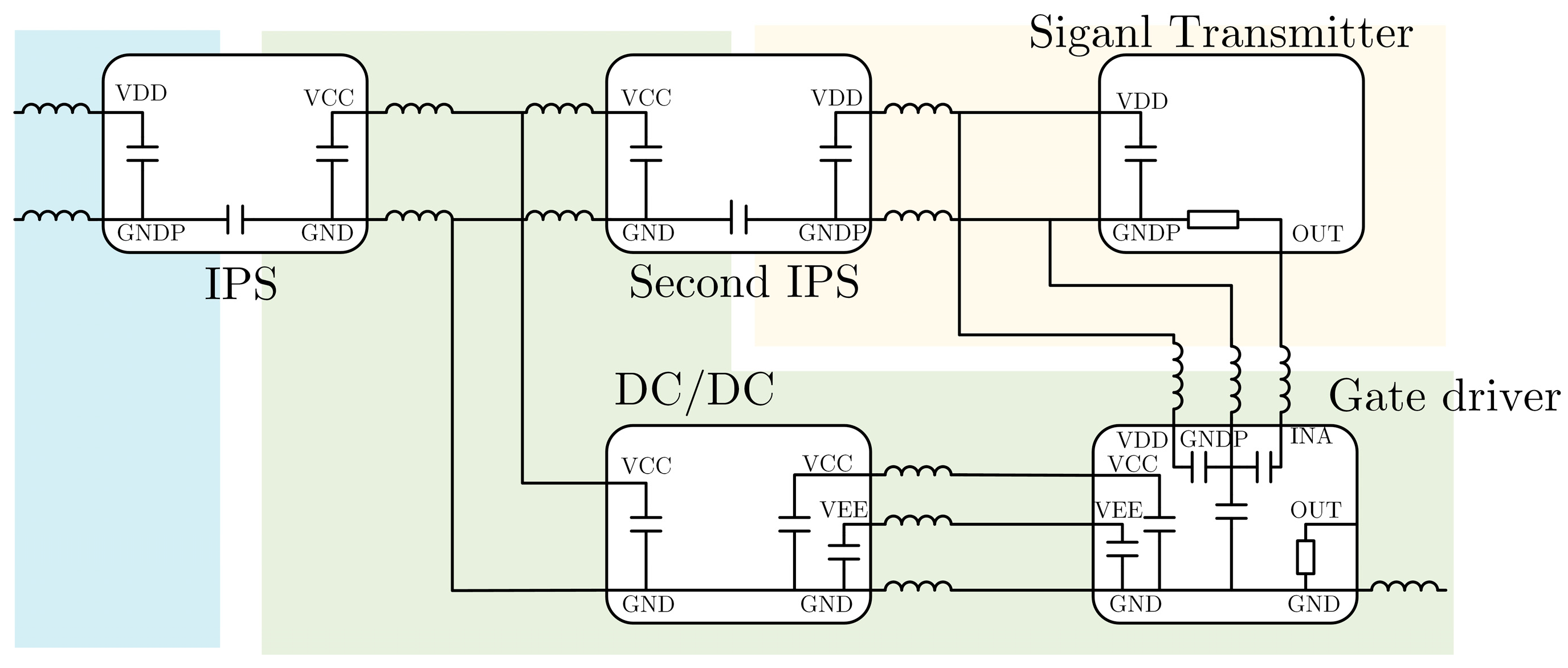
Figure 4 illustrates the electromagnetic network model incorporating various functional modules and parasitic inductance distribution in the high-side driver circuit architecture. Under high-frequency operation, while the parasitic resistance of PCB traces increases due to the skin effect, the inductive reactance becomes the dominant impedance characteristic, rendering the parasitic resistance negligible for most power supply traces. However, special consideration must be given to the extended connection between the driver IC and the SiC MOSFET source pin in this PCB design, where the substantial trace length results in non-negligible parasitic parameters that require explicit modeling in the analysis.
To simplify the interference electromagnetic model, the following simplifications are made:
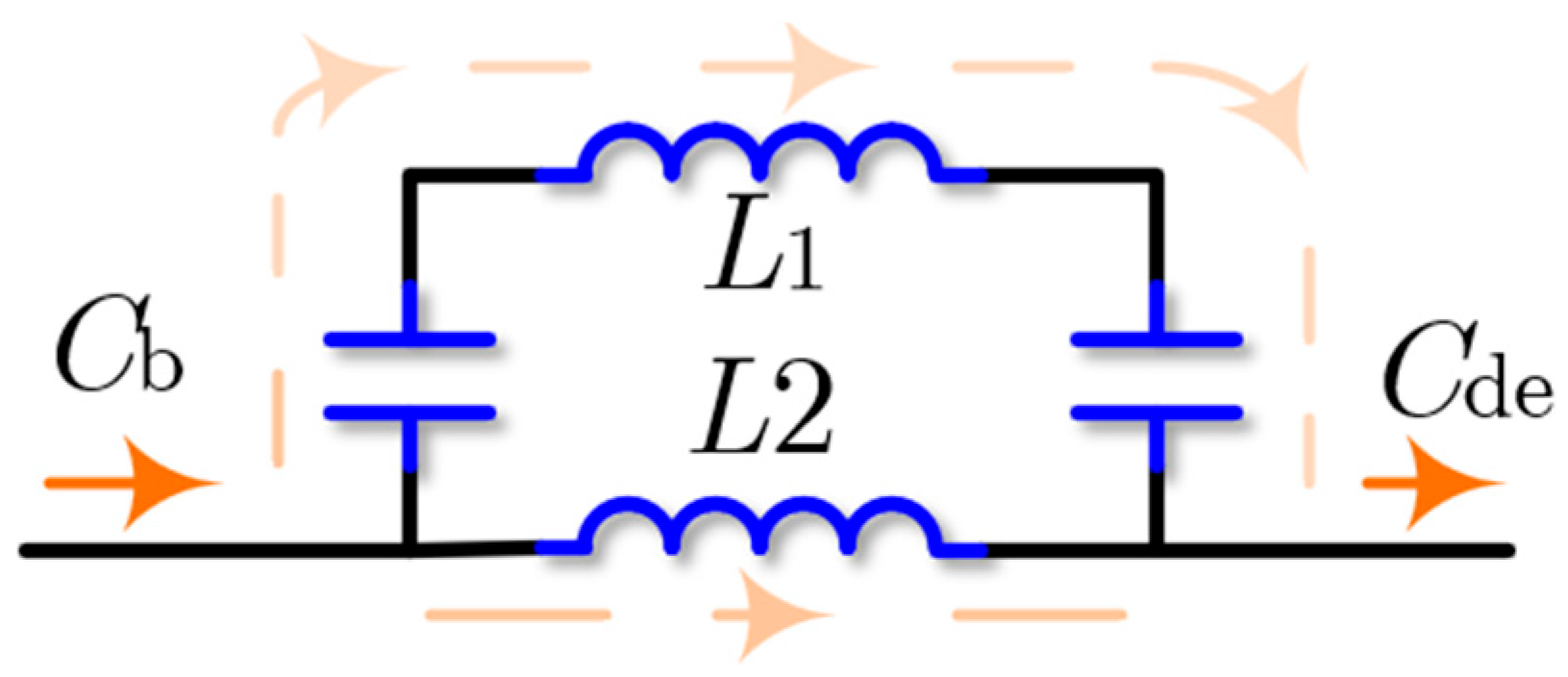
(1) Taking the electrical connection between the isolated power supply and the DC/DC power module shown in Figure 5 as an example. Figure 6 illustrates the power traces between the isolated power supply and the DC/DC module. In this configuration, (1) Cb serves as the output filter capacitor of the isolated power supply with a typical capacitance in the microfarad range, (2) L1 and L2 represent the parasitic inductances (typically several nanohenries) of the auxiliary power supply traces, and (3) Cde functions as the DC/DC module’s decoupling capacitor, also in the microfarad range. At high frequencies, the significantly lower impedance of both the filter and decoupling capacitors compared to the trace parasitic inductances effectively shorts these capacitive elements. This simplification allows the common-mode impedance of the branch in Figure 6 to be represented by the equivalent inductance Lp in Figure 7.
(2) In the fiber optic conversion circuit, data transmission is achieved through optical fibers, which means there is no direct electrical connection with the transmitting end. The coupling capacitance between the circuit and the fiber optic transmitting circuit is nearly zero. Therefore, the optical signal input path in the fiber optic conversion circuit can be regarded as an open circuit.
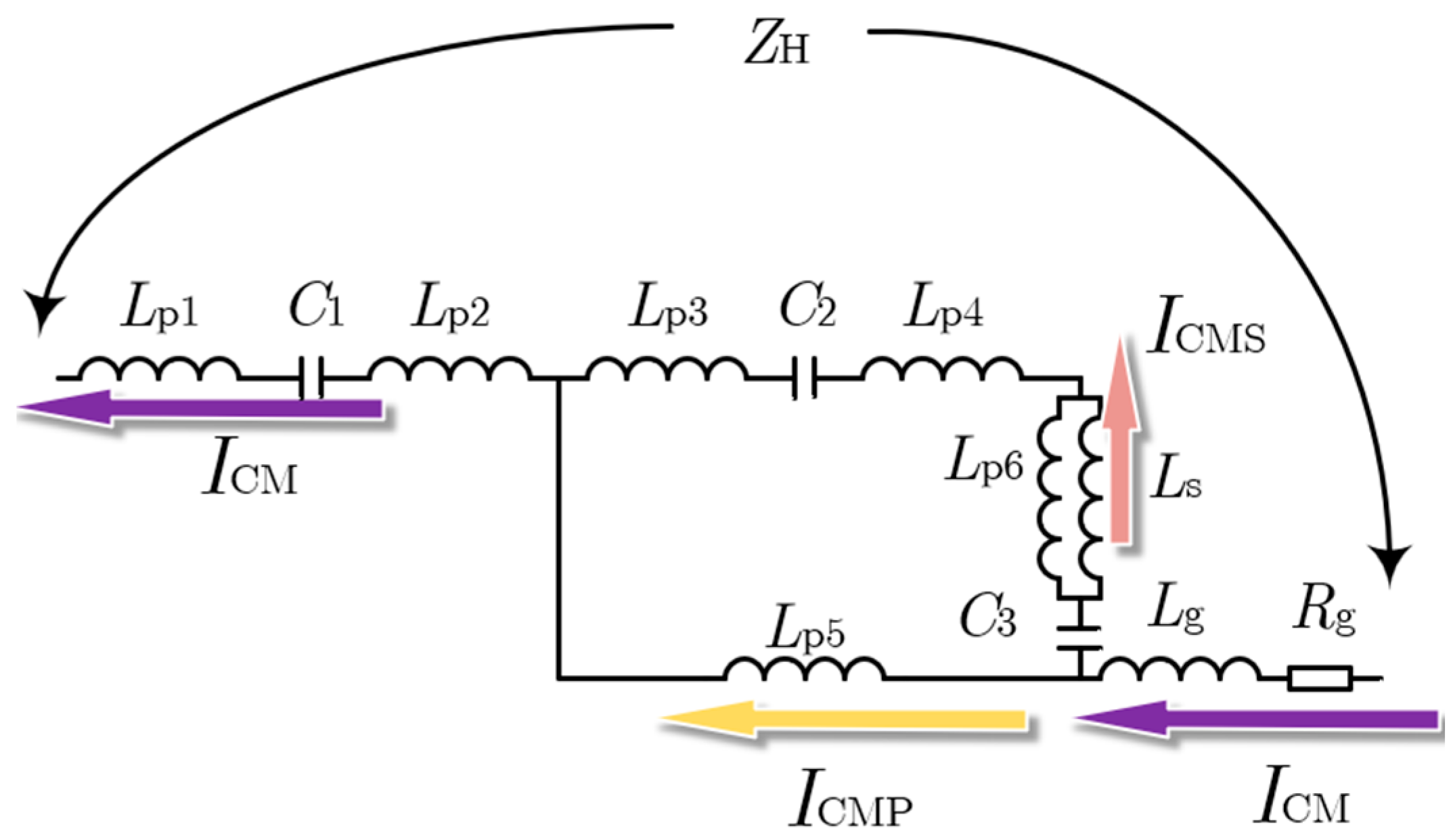
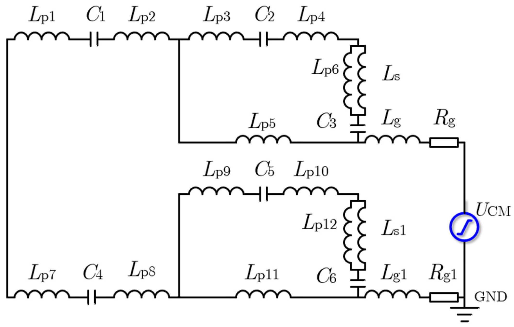
Following the above principles, the high-side drive circuit can be simplified into the network model shown in Figure 8, where each component represents the physical meanings listed in Table 1.
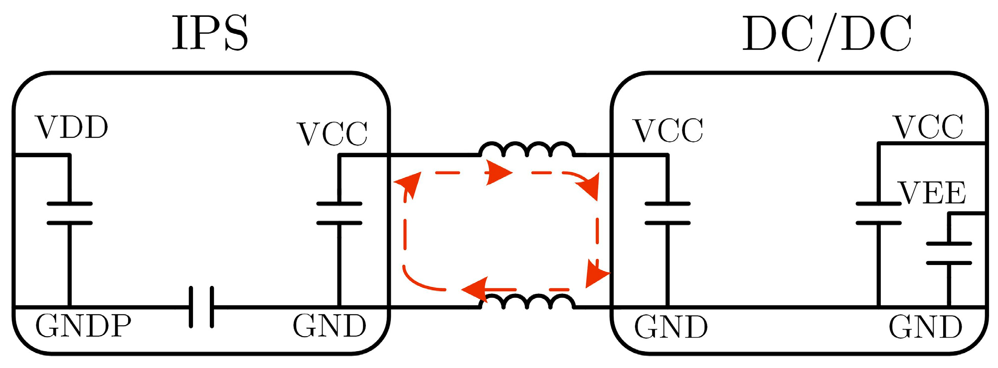
The path of common-mode interference current within the driver circuit is shown in Figure 8. The common-mode interference current enters from the driver output port, passes through the driver IC, and flows into both the power branch and the signal branch. Since the fiber-optic transmission is treated as an open circuit, the common-mode interference current in the signal branch bypasses the fiber-optic decoding chip and flows back to the input of the isolated power supply via the coupling capacitor of the secondary isolated power supply. In the power branch, the common-mode current flows back to the output port of the isolated power supply through the driver IC driving circuit. These two parts of the interference current jointly flow back to the weak ground through the coupling capacitor of the isolated power supply. It is noteworthy that, because the signal control side is formed by the floating ground created by the secondary isolated power supply and isolated gate driver IC, with the total isolation capacitance being less than 1 pF, the interference current in the signal branch is much smaller than that in the power side at high frequencies. Since the high-side driver board is consistent with the low-side driver board, once the electromagnetic network model of the high-side driver board is obtained, the complete common-mode interference network model of the half-bridge submodule can be derived, as shown in Figure 9.

2.2. Characteristics of Common-Mode Current Magnitude in Drive Circuits

Due to the presence of three capacitors in the circuit, the order of the circuit may become excessively high. Therefore, the model can be further simplified based on the existing conditions. It is known that the total isolation capacitance of the signal branch is less than 1 picofarad, while the parasitic inductance of the power branch in parallel with it is several nanohenries. At high frequencies, the impedance of the signal branch is generally greater than that of the parallel power branch, allowing the signal branch to be considered open. This assumption is further validated by the complete simulation model established subsequently.
The first step is to model the interference signal source. When Q1 is off and Q2 is on, the midpoint of the half-bridge serves as the reference potential. Upon receiving the switching signal, the midpoint voltage of the half-bridge rises rapidly until it reaches the bus voltage Udc. During this rise, an overshoot voltage is also generated. Most studies on modeling the midpoint voltage variation of the half-bridge use a trapezoidal wave to simulate this behavior [10], while some researchers model the overshoot voltage using a decaying sinusoidal wave. Since this paper primarily investigates the main factors influencing the common-mode current amplitude and suppression methods, a trapezoidal wave is chosen to model the interference source. The resulting interference voltage UCM is given by Formula (1), where tsw is the time required for the midpoint voltage to rise from zero to Udc.
U CM = U dc t sw t t t sw U dc t > t sw
When the signal branch is open-circuited, the total common-mode impedance ZCM of the high- and low-side driver boards can be expressed as follows:
Z CM = s L eq + 1 / s C eq + R eq L eq = 2 × L p 1 + L p 2 + L p 5 + L g
where Leq is the equivalent series inductance, Ceq is the equivalent series capacitance, and Req is the equivalent series resistance.
L eq = 2 × L p 1 + L p 2 + L p 5 + L g
C eq = C 1 2
R eq = 2 R g
Calculate the common-mode interference current flowing through the isolation power supply’s coupling capacitor using the complex frequency domain method:
i CM = i CM 1 = L 1 U dc / t sw s 2 R eq + s L + 1 s C eq ( 0 t t sw ) i CM 2 = i CM 1 i CM 1 ( t t sw ) ( t > t sw ) U dc t sw C eq ( 1 1 sin φ e t τ sin ( ω t + φ ) ) ( 0 t t sw ) U dc t sw C eq ( 1 sin φ e t t sw τ sin ( ω ( t t sw ) + φ ) 1 sin φ e t τ sin ( ω t + φ ) ) ( t > t sw )
To obtain the amplitude characteristics of the common-mode current, we perform a derivative analysis of the common-mode interference current iCM and obtain the derivative of the common-mode interference current, as shown in the equation. Since in the RLC circuit, during the current oscillation process, the resistance is much smaller compared to the inductance and capacitance impedance, it exhibits underdamping. Therefore, the maximum current typically occurs at the first peak and then gradually decays. Hence, only the derivative of icm1 is considered here.
d i CM 1 d t = U dc t sw C eq ( 1 τ sin φ e t τ sin ( φ + ω t ) ω sin φ e t τ cos ( φ + ω t ) )
When the derivative of the common-mode current iCM equals 0, it corresponds to the moment when iCM reaches its maximum value. The solution for t0 is as follows:
t 0 = π ω
In the case of underdamping, t0 is less than tsw. Therefore, by substituting the maximum value moment t0 into the common-mode current iCM1, the amplitude of the common-mode current ICM can be obtained as follows:
I CM = C eq U dc t sw ( e - π ω τ + 1 )
Leq is in the nanohenry (nH) range, Ceq is in the picofarad (pF) range, and Req is in the milliohm (mΩ) range. Based on experience, the typical parameter ranges are 1 < Ceq < 40 pF, 5 < Leq < 200 nH, and Req = 0.5 Ω for general PCB driver circuits. Equation (9) can be simplified to Equation (10). Additionally, the figure indicates that the error caused by this approximation is less than 4%.
I CM = 2 C eq U dc t sw = C 1 U dc t sw

2.3. Simulation and Common-Mode Current Spectrum Analysis

After establishing a complete electromagnetic network model for the half-bridge submodule, to obtain the actual common-mode interference current waveform through simulation software and verify the magnitude characteristics of the common-mode interference current, it is necessary to obtain the actual values of the parameters listed in Table 2. Among these, C1, C2, and C3 are the parasitic parameters of the devices, which are generally tested and specified by the manufacturer in the accompanying datasheets. Therefore, the typical values of these parameters can be obtained by consulting the device datasheet. The specific model of the isolated power supply, as well as the values of C1, C2, and C3, are provided in the table below.
It is impractical to obtain the parasitic inductance and other parameters of the power and signal lines of a PCB board through physical calculations. Therefore, researchers typically use finite element simulations to acquire the parasitic parameters of the PCB board. Q3D is common software used for extracting PCB parasitic parameters, simulating the actual physical fields. Before using Q3D to extract parasitic parameters, it is necessary to first import the PCB file into Ansys Slwave for preprocessing and extracting the wiring network to be analyzed, as shown in Figure 10a.
After completing the above steps, the preprocessed file can be imported into the Q3D software to extract all the required parameters. Table 3 presents the parameter values of the power traces in the impedance model shown in Figure 10b. During the extraction of parasitic parameters, it is important to note that parasitic resistance also exists on the traces. However, on the one hand, the parasitic resistance of short traces is very small. On the other hand, for high-frequency signals, the parasitic inductance impedance of the traces is much greater than the parasitic resistance. Therefore, the parasitic resistance in short traces is generally negligible.
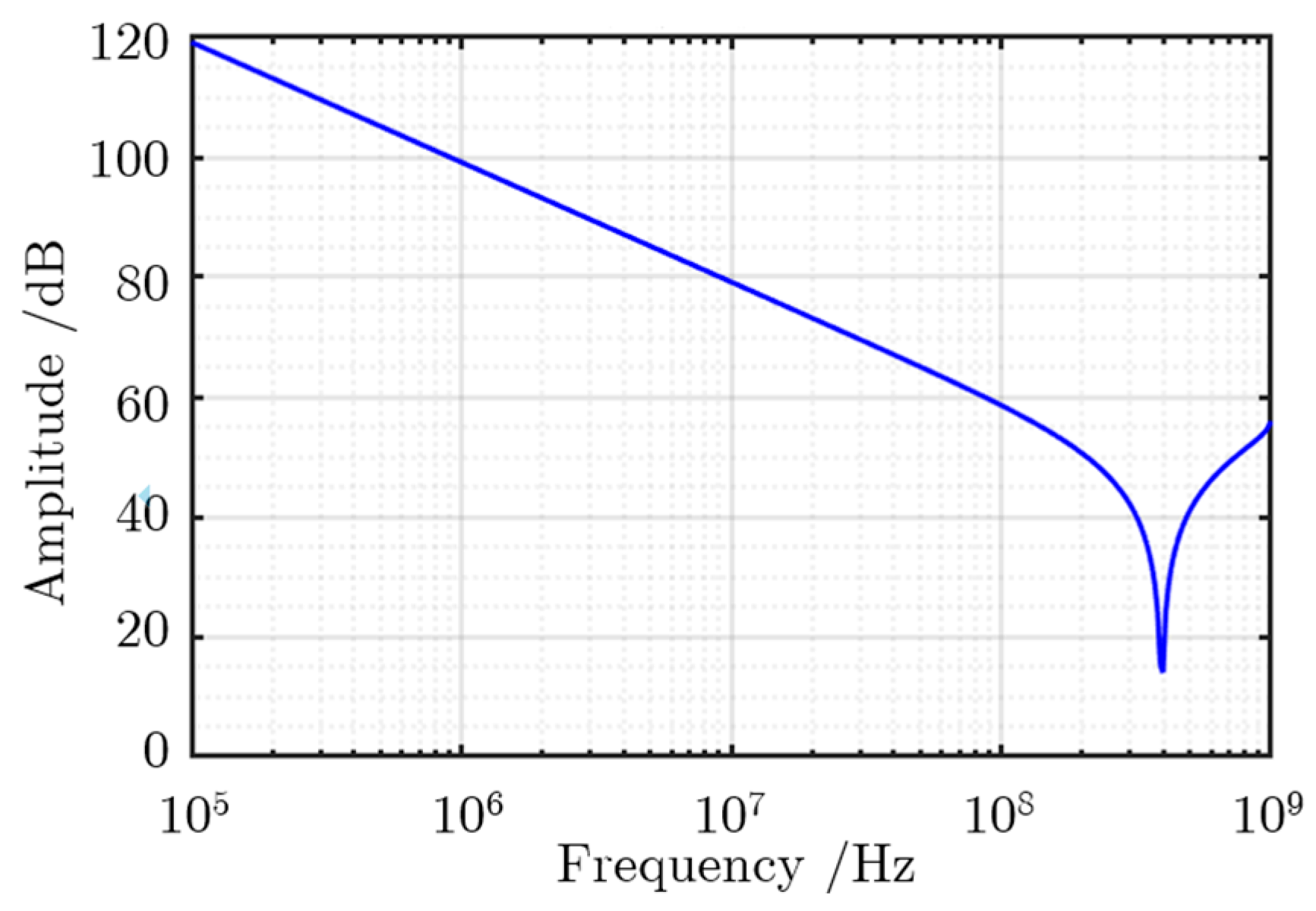
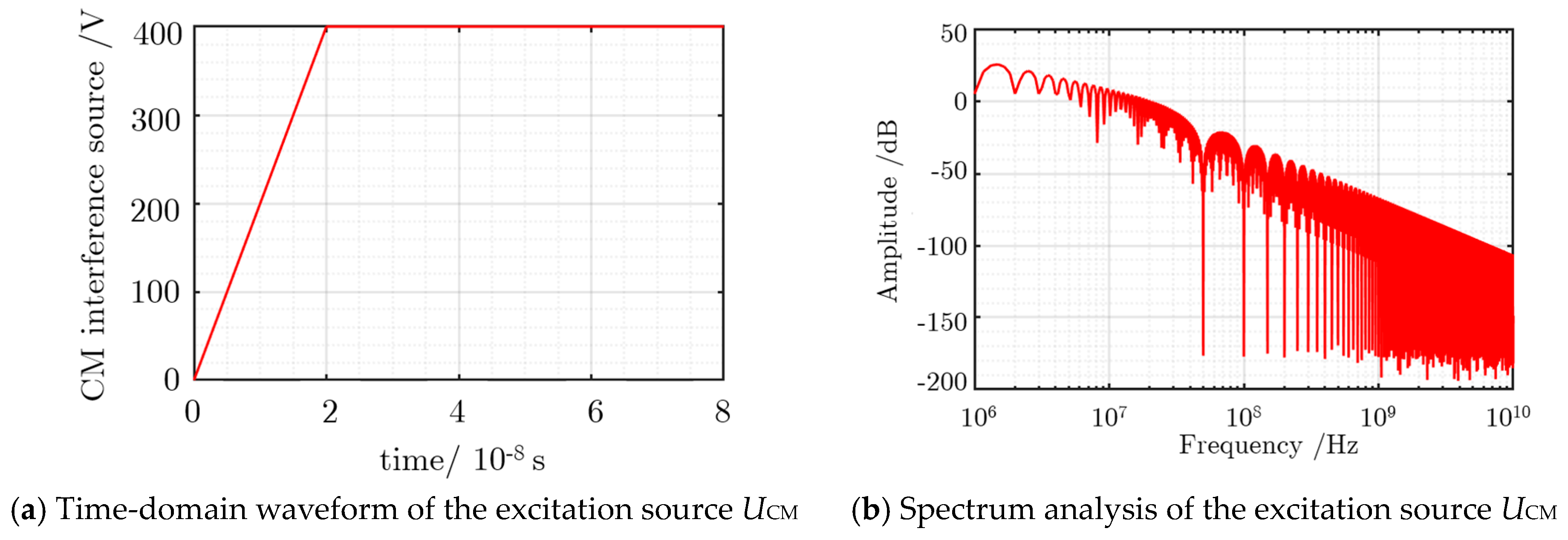
By substituting the parameters extracted from Table 3 into the impedance model in Figure 8, the impedance curve of the driving common-mode conduction loop is obtained, as shown in Figure 11. From the figure, it can be seen that the impedance of the conduction loop decreases in the low-frequency range with a slope of 20 dB per decade. When the frequency reaches the resonant frequency, the impedance achieves its minimum value. Afterward, in the high-frequency range, the impedance increases again with a slope of 20 dB per decade. The excitation source, based on experimental experience, is set with an amplitude of 400 V and a rise time of 20 ns, generating a dv/dt of 20 V/ns. The time-domain and frequency-domain analyses of the excitation source are shown in Figure 12. From the frequency spectrum of the excitation source, it can be observed that the spectrum decreases overall with a slope of 50 dB per decade.
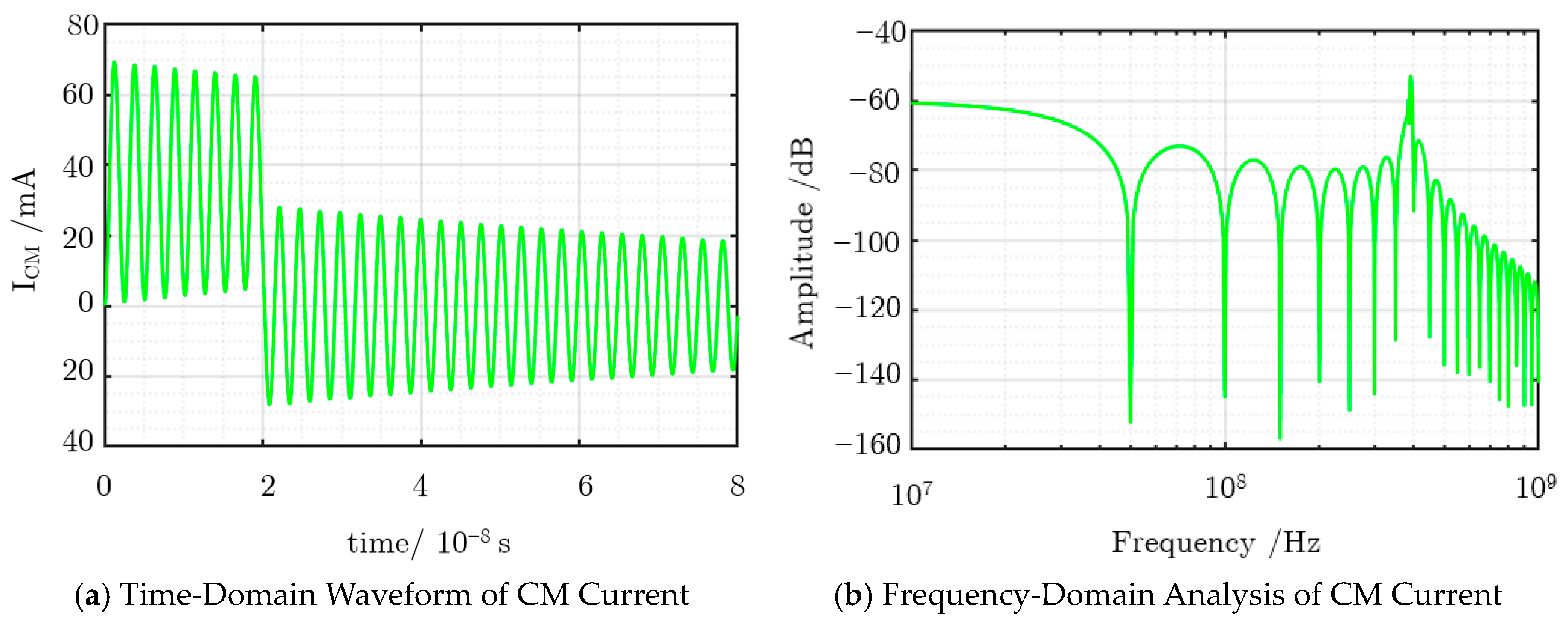
After configuring the excitation source, a complete simulation model was established using LTspice—a widely adopted power electronics simulation tool known for its high speed and precision. Based on the previously determined circuit parameters, the simulation was conducted over an 80 ns duration. The resulting common-mode current waveform across the isolated power supply is depicted in Figure 13a, revealing a peak current of 69.57 mA that matches the theoretically derived amplitude characteristics. Furthermore, the frequency spectrum in Figure 13b demonstrates that the common-mode current reaches its maximum gain precisely at the resonant frequency of the common-mode conduction impedance ZCM.
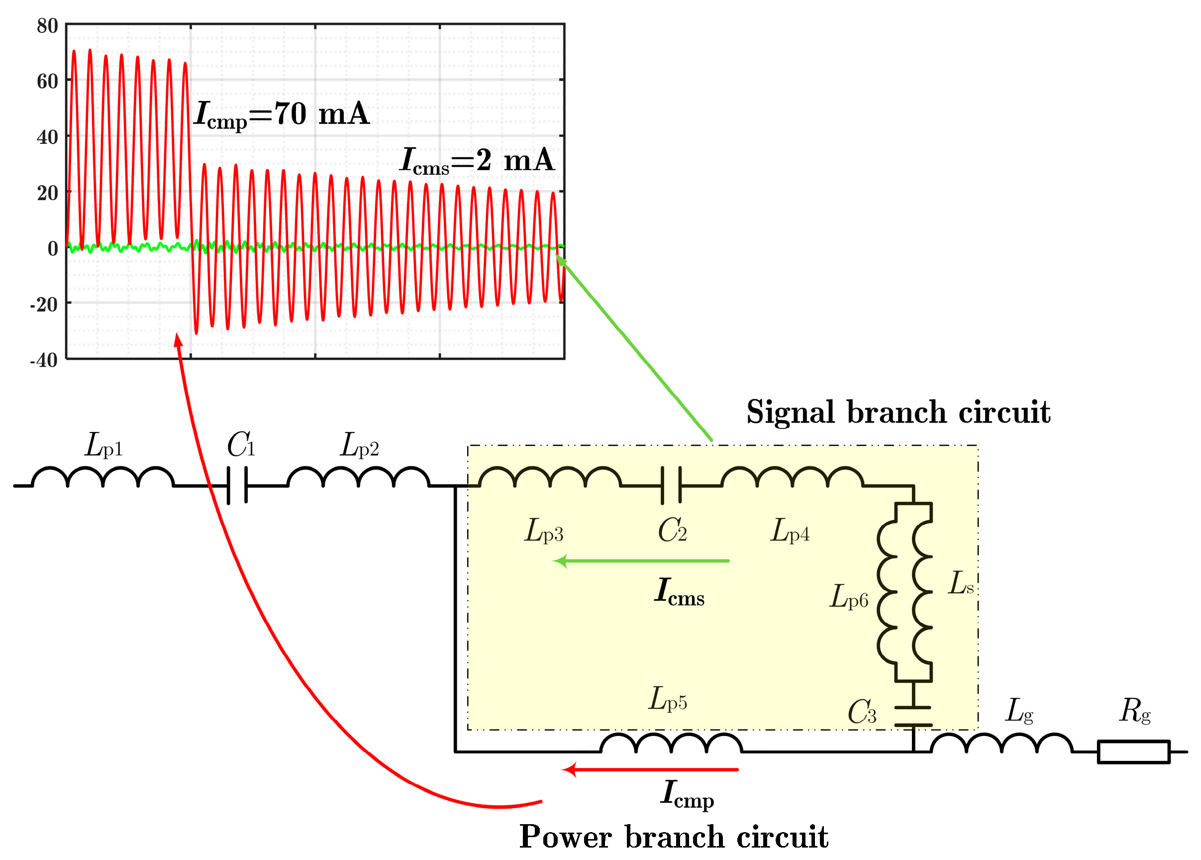
To verify the suppression effect of the proposed driver architecture on the common-mode current on the signal side, the simulation model retains the signal control branch without opening the circuit, as shown in Figure 14. By observing the common-mode current magnitude on the control side branch and the common-mode current magnitude on the power side branch below, it can be seen that the common-mode current magnitude on the signal control side is approximately 2 mA, while the common-mode current magnitude on the power side branch below is about 70 mA, which is 35 times greater than the former. Therefore, it is reasonable to open the signal control side when performing mathematical modeling of the drive circuit, and this also proves that the proposed driver architecture can effectively reduce the common-mode interference current flowing through the control side.
Equation (10) indicates that the primary external factor influencing the magnitude of the common-mode current is the coupling capacitance value of the isolated power supply. To explore the effects of other parameters in the drive circuit on the common-mode current magnitude, this section will use LTspice to scan several key parameters of the half-bridge submodule network model, such as Lp1 and Rg, shown in Figure 15. Additionally, to verify the above conclusion, a parameter scan of the isolated power supply coupling capacitance C1 will also be conducted. The results are shown in Figure 15.
As can be seen, the parasitic inductance Lp1 and parasitic resistance Rg of the PCB power supply line have a minimal effect on the magnitude of the common-mode current within their normal variation range (due to different PCB designs causing different parasitic parameter values). In contrast, when the isolated power supply coupling capacitance changes, the magnitude of the common-mode current closely follows these changes, showing an almost linear relationship. Therefore, it can be concluded that the primary factor influencing the magnitude of the common-mode current is the isolated power supply coupling capacitance.
It should be noted that within the normal PCB design range of Rg, it will not significantly affect the common-mode current. However, when a large equivalent resistance (such as series common-mode inductance) is introduced into the common-mode impedance loop by other means, the magnitude of the common-mode current will decrease significantly. Introducing a large pure inductance into the equivalent circuit, however, will not reduce the common-mode current magnitude but instead cause persistent oscillations in the common-mode current.

3. Hardware Design of Half-Bridge Power Module

This section provides a detailed introduction to the design process of the basic unit in the modular multilevel converter (MMC) topology, commonly referred to as the MMC submodule. The submodule designed in this work adopts a half-bridge topology and is therefore referred to as the half-bridge submodule in the following discussion. This section includes the following steps: first, the selection of power devices; second, the design of the driver circuit and the choice of an isolated power supply scheme; and finally, the design of the DC bus capacitor.

3.1. Selection of Power Device

Table 4 provides a comparison of three commercial 3.3 kV SiC power devices and their key performance parameters. The G2R120MT33J, manufactured by GeneSiC Semiconductor, exhibits the highest current-carrying capacity with a maximum conduction current of 35 A. However, its relatively high cost limits its economic feasibility. On the other hand, the MSC400SMA330B4 from Microchip Technology delivers a maximum conduction current of 11 A with an on-resistance of 400 mΩ, offering a more cost-effective solution. Based on these considerations, the MSC400SMA330B4 is selected for this design.

3.2. Selection of Isolated Power Supply

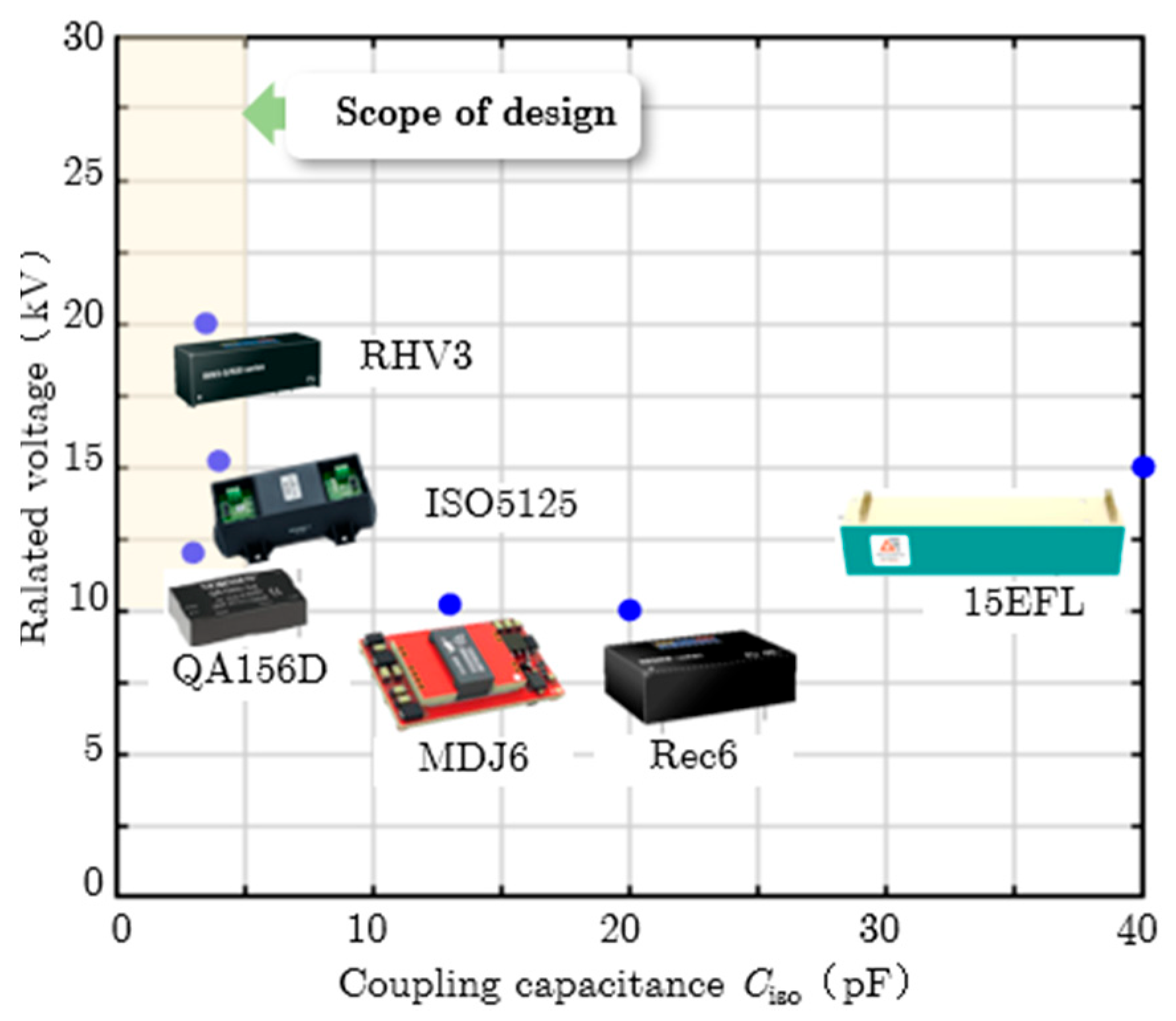
Compared to traditional silicon power devices, SiC power devices exhibit significantly higher switching speeds, which substantially increase dv/dt stress on the gate driver circuit. This places stricter requirements on the Common Mode Transient Immunity (CMTI) performance of the gate driver circuit. As a critical component that powers the gate driver circuits, the isolated power supply (IPS) in high-voltage SiC applications must meet an isolation voltage rating above 10 kV to block the high-voltage potential difference between the high-potential side of the main circuit and the low-potential side of the control circuit. Additionally, it must achieve a coupling capacitance below 5 pF to effectively suppress common-mode currents. Figure 16 compares six commercially available IPS solutions with isolation voltages exceeding 10 kV. The analysis reveals that the RHV3 series demonstrates superior performance in insulation capability, coupling capacitance, and cost-effectiveness. Specifically, it achieves a coupling capacitance of only 3 pF and an insulation voltage rating of up to 20 kV. Therefore, the RHV3 series is selected as the isolated power supply solution for this application.

3.3. Gate Driver Design

Figure 17 illustrates the schematic diagram of the single-device gate driver. This design achieves high performance through precise component selection and an optimized power supply grounding structure.
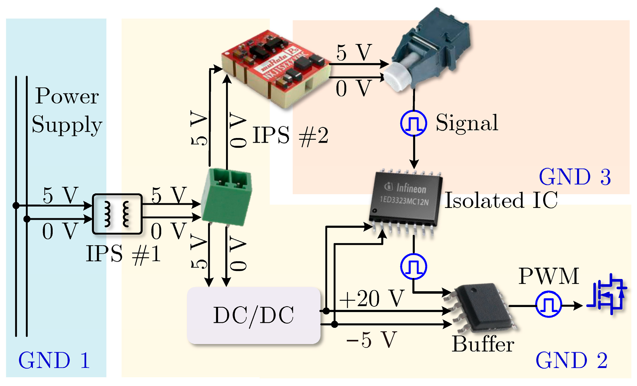
The isolated gate driver IC used in the design is the 1ED3323MC12NXUMA1, which offers a withstand voltage of 6.84 kV (RMS) and a common-mode transient immunity exceeding 300 kV/μs, with a coupling capacitance of 1.4 pF. In Figure 2, boxes of different colors represent distinct grounding structures: GND1 corresponds to the cabinet power ground; GND2 shares the potential of the MOSFET drain; GND3 serves as the signal ground, which is established by the isolated gate driver IC and IPS#2 (NXE2S0505MC, coupling capacitance is 2.1 pF). When the MOSFET is conducted, the potential of GND2 significantly increases, requiring IPS#1, which connects GND1 and GND2, to withstand several kilovolts of potential difference. IPS#1 is selected from the RHV3 series as described in the previous section, with a voltage rating of 20 kV and a coupling capacitance of 3 pF. Due to the low shielding capacitance of the gate driver IC and the secondary DC/DC converter, common-mode noise currents predominantly flow through the low-impedance paths indicated in Figure 17, bypassing the signal ground. Additionally, some common-mode noise also flows through the primary DC/DC converter. To achieve a high output current capability, a current amplifier (model IXDN614SI) is added downstream of the isolated gate driver IC. This amplifier features a rise time of 25 ns and a fall time of 18 ns, meeting the driving requirements of SiC MOSFETs. Furthermore, a gate resistor with a resistance value of 20 Ω is selected. The short-circuit protection method adopts desaturation protection. Considering the balance between noise immunity and the protection speed, the desaturation response time is set to 1.1 μs.

3.4. Selection of Capacitor

Film capacitors, with their high voltage resistance, low loss, and excellent high-frequency performance, have become the preferred choice for capacitor solutions in converter designs based on SiC MOSFETs. They are particularly suitable for applications requiring high frequency, high voltage, and high power density. This section introduces three capacitor design schemes, as shown Figure 18. The 1st option uses two 1.5 kV/200 μF cylindrical film capacitors connected in series, forming a capacitor module with a rated voltage of 3 kV, a capacitance of 100 μF, and a submodule volume of 2.23 L. The 2nd option directly adopts a single 3 kV/200 μF capacitor with an overall volume equivalent to 200 μF. The 3rd option integrates six film capacitors of type C4AQSEW5400A3B, achieving a rated voltage of 3 kV and a capacitance of 60 μF.
Capacitor design requires attention to more than just the rated voltage and capacitance. Additional key parameters, including the overcurrent capacity, equivalent series inductance (ESL), equivalent series resistance (ESR), and volume, must also be taken into account. Capacitors with low ESL and ESR help suppress voltage overshoot and reduce losses. A smaller volume improves the integration level of submodules, contributing to higher system power density. A comparison of the three schemes (as shown in Table 5) indicates that 3rd option offers the best performance in critical parameters. It offers the lowest ESL and volume, as well as a comparatively low ESR. Although its capacitance is the lowest, it fully meets the requirements for use with a 3.3 kV/11 A SiC MOSFET, demonstrating strong applicability and competitiveness.

3.5. Module Integration

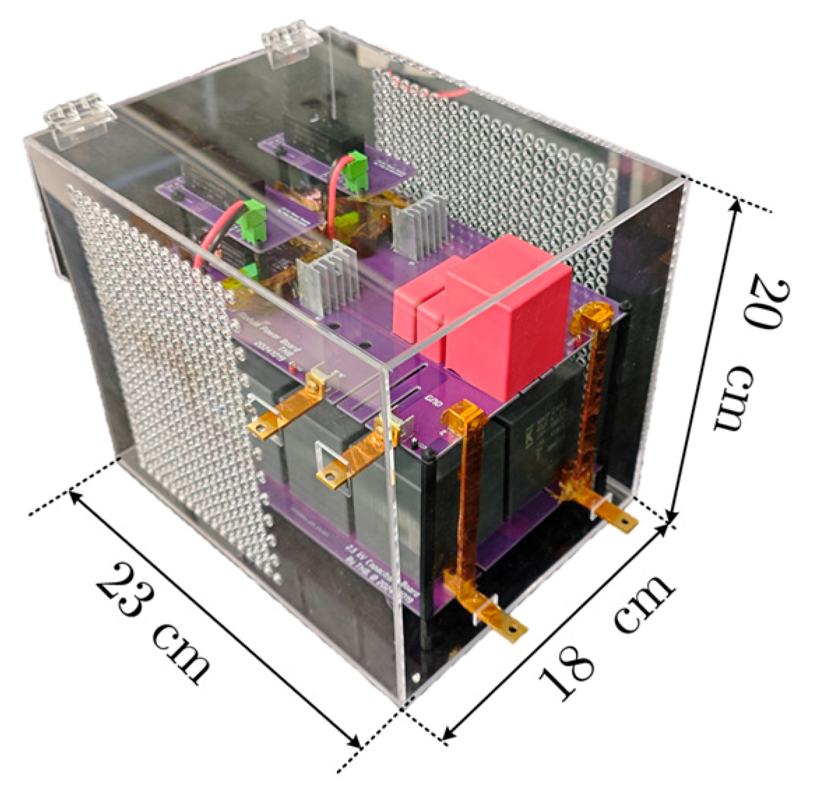
This section presents the 3D modeling and prototype assembly of the submodule using SolidWorks 2024, as shown in Figure 4. Figure 19a illustrates the main components of the submodule: two IPS boards, two GD boards, a main power board, and a bus capacitor board. The main power board integrates SiC MOSFETs, heat sinks, and decoupling capacitors. It is connected to the bus capacitor board by copper bars, which minimize parasitic inductance. Figure 19b shows the electrical connection points of the submodule. The final physical prototype is shown in Figure 20. An acrylic enclosure was added to the submodule. In the future, a fan may be installed in the enclosure to reduce the operating temperature of the power devices. The integrated prototype has a volume of 8.28 L.

4. Experimental Validation

This section introduces the submodule prototype. A buck converter test platform is then built to verify the current-carrying capability. Finally, a 2 kV high-voltage double-pulse test platform is set up to test the insulation performance. The high-voltage SiC submodule testing platform established in this work is shown in Figure 21. The high-voltage DC power supply used is the PA4012 model manufactured by PINTECH (Taiwan, China). The oscilloscope is a Tektronix (Beaverton, OR, USA) MDO34 series with a bandwidth of 200 MHz. The auxiliary power supply is the UTP3305-II series produced by UNI-T (Dongguan, China). These specifications have also been updated in the revised manuscript accordingly.

4.1. Buck Test

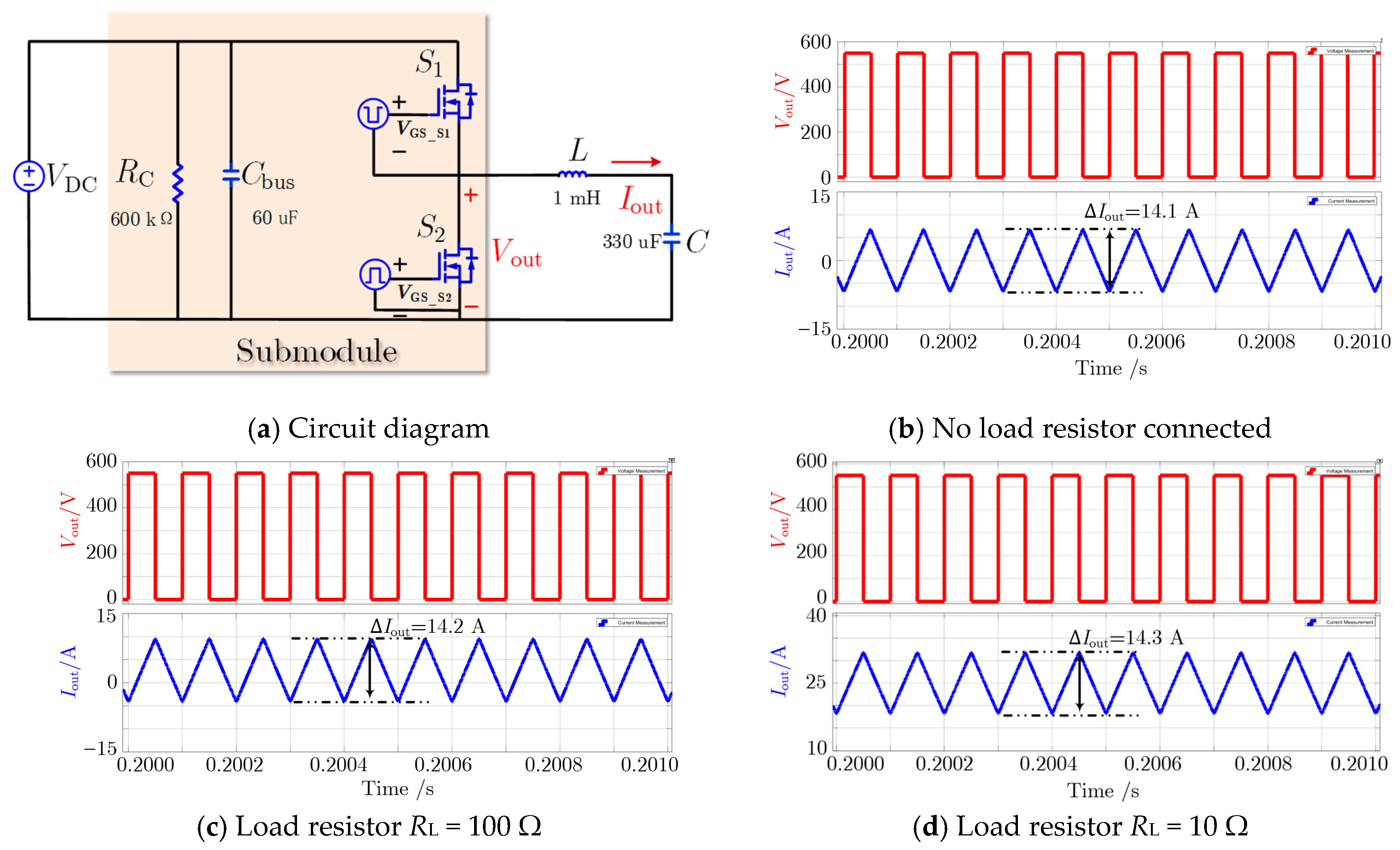
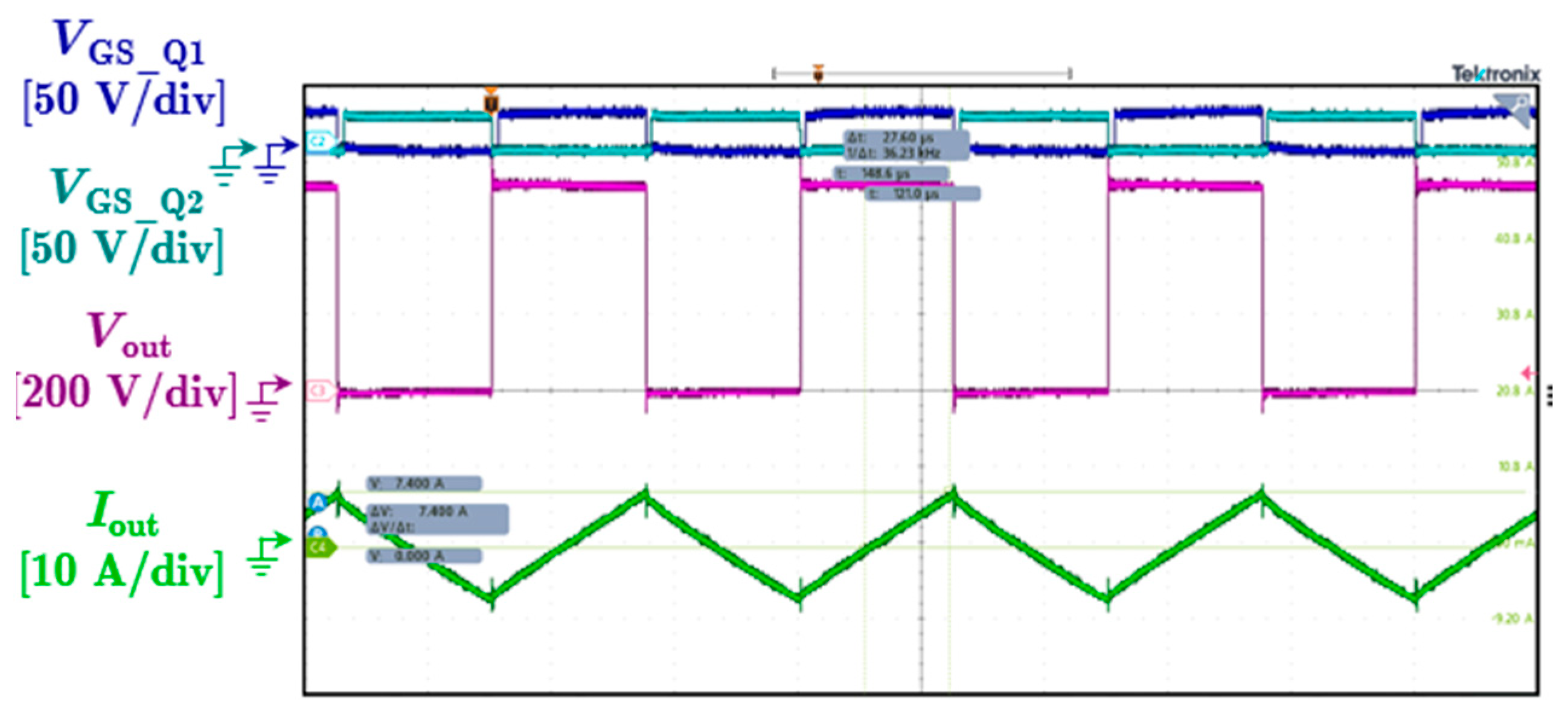
To evaluate the reliability of the designed submodule under bipolar and time-varying current conditions during actual operation, a buck converter test is designed and implemented in this section. The buck converter is a widely used experimental setup for such evaluations. The schematic of the test circuit is shown in Figure 22a. The bus voltage is set to 550 V, and the submodule operates at a frequency of 10 kHz with a fixed duty cycle of 0.5. During testing, an LC load is connected at the output to simulate reactive power conditions, thereby enabling bidirectional current flow. The inductance of the load inductor is 1 mH, and the capacitance of the load capacitor is 330 μF. The use of an LC load ensures that no active power is introduced; the inclusion of a resistive component would alter the output current waveform. Figure 22b,c,d illustrate the cases of an open load, Rload = 100 Ω, and Rload = 10 Ω, respectively. Simulation results show that under different loading conditions, the peak-to-peak value of the output current remains constant, with the current ripple ΔIout maintained at approximately 14 A. However, the positions of current peaks and zero-crossing points vary with the load. Under heavy load conditions, the output current tends to flow in one direction, and the current peak increases significantly. This operating condition may impose excessive current stress on the devices. The experimental results, shown in Figure 23, are consistent with the simulation results. The test lasted for approximately 30 min, and the results reflect the good current-handling capability of the designed power module.
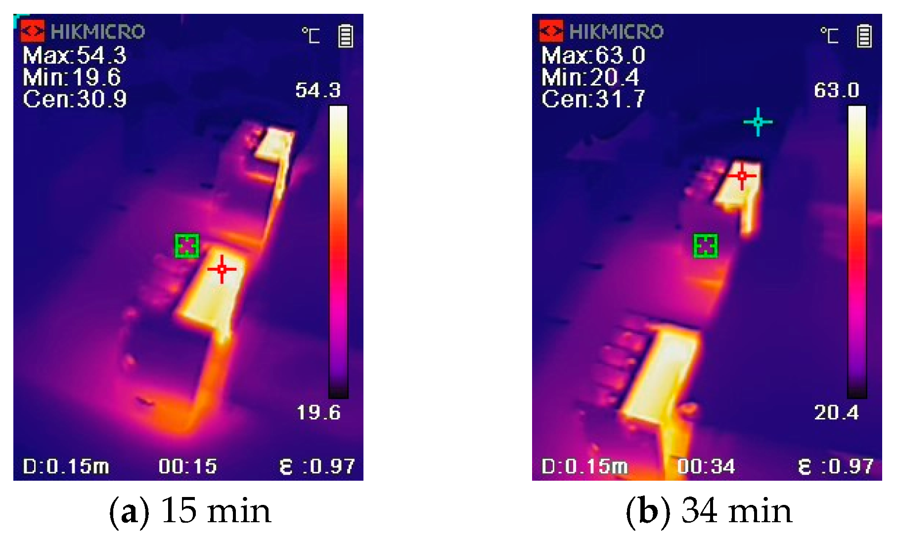
Figure 24 shows the thermal distribution of the power device after 15 min and 34 min of operation. After 34 min, the maximum temperature of the power device reached 63 °C. The test results indicate that the designed submodule achieved reliable operation in the continuous buck converter test.

4.2. Double Pulse Test

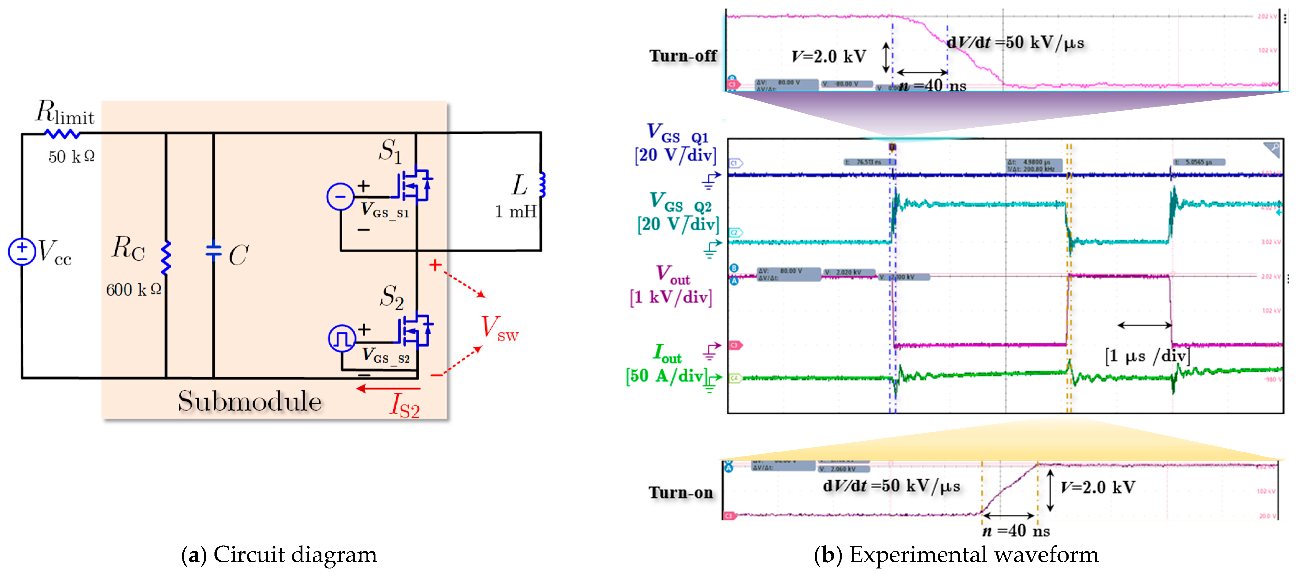
Double pulse tests are commonly used to evaluate the dynamic characteristics of the devices, analyze parasitic oscillations and EMI issues, and optimize the gate driver design. The submodule was tested using double pulse tests at a DC voltage of up to 2.0 kV. Its functionality, common mode noise immunity, and insulation capability were evaluated. The test circuit diagram is shown in Figure 25.
In the tests, both S1 and S2 were controlled by gate drivers, but S1 remained continuously off. S2 was driven with a first pulse time of 3 μs, an off time of 2 μs, and a second pulse time of 1 μs. The double pulse test waveforms at 2.0 kV and 11 A are shown in Figure 10. During the turn-on transient, the switching dv/dt reached 50 kV/μs, with a voltage overshoot of 200 V, while during the turn-off transient, the dv/dt reached 37.5 kV/μs, with a voltage overshoot of 140 V. The test results verified the driving functionality of the driver circuit and showed that the main circuit has low parasitic parameters. In the future, the bus voltage of the submodule will be further increased to verify the insulation design of the submodule.

4.3. Measurement of Common-Mode Current

The measurement was conducted using a double-pulse test platform with the bus voltage set to 400 V. During the double-pulse test, when the lower transistor is turned on, the midpoint voltage drops. The voltage fall time measured by the oscilloscope is 20 ns, resulting in a dv/dt of 20 V/ns. The direction of the common-mode current is also reversed, as shown in Figure 26. From the figure, the measured amplitude of ICM is 68 mA, which is consistent with the theoretical calculation, thereby validating the accuracy of the simulation model.
As shown in Table 6, without employing additional shielding measures, the equivalent coupling capacitance of the driver circuit designed in this work is 3.4 pF. In contrast, under the same unshielded condition, the equivalent coupling capacitance achieved by the custom transformers in References [1] and [2] is 6.5 pF and 7.2 pF, respectively. These results indicate that even using a commercial power module, the proposed method demonstrates superior performance in suppressing common-mode currents.

5. Conclusions

This paper focuses on the common-mode interference in the gate driver circuit of high-voltage SiC devices. A mathematical model and simulation analysis are carried out. Based on the architecture of the gate driver in this work, a modeling method for the common-mode interference in the half-bridge submodule based on high-voltage SiC MOSFET is proposed. Parasitic inductances of the PCB driver circuit are extracted using Q3D to optimize model parameters. The impedance characteristics are analyzed to identify the main factors influencing the formation of high common-mode currents. On this basis, a design method for low common-mode current in the half-bridge submodule based on high-voltage SiC MOSFET is proposed, including optimizing the driver circuit architecture, capacitor design, and submodule integration. Finally, a compact prototype of a 3.3 kV high-voltage SiC submodule is developed. Its performance is verified through double-pulse testing and steady-state buck circuit testing. Simulation and experimental results show that the amplitude of the common-mode current is mainly determined by the coupling capacitance of the auxiliary power supply and follows a certain proportional relationship. The developed SiC submodule achieves fast switching at 50 kV/μs under a 2 kV DC bus voltage. It demonstrates excellent thermal stability and low common-mode current characteristics, confirming the effectiveness of the proposed model and design method. This study provides theoretical and technical support for characterizing and evaluating common-mode currents in high-voltage SiC devices and designing highly reliable SiC submodules.

Author Contributions

K.X.: Formal analysis, Validation; H.T.: Methodology, Validation; Z.C.: Writing—review & editing; Y.Z.: Writing—review & editing; J.P.: Funding acquisition, Conceptualization. All authors have read and agreed to the published version of the manuscript.

Funding

This work is sponsored by the Science and Technology Program of China Southern Power Grid Co., Ltd. (H20241983).

Data Availability Statement

The original contributions presented in this study are included in the article. Further inquiries can be directed to the corresponding author.

Conflicts of Interest

Authors Kai Xiao, Zhihong Cai and Yansheng Zou were employed by the China Southern Power Grid Company Limited. The remaining authors declare that the research was conducted in the absence of any commercial or financial relationships that could be construed as a potential conflict of interest.

References

  1. Pan, J.; Ke, Z.; Al Sabbagh, M.; Li, H.; Arjun Potty, K.; Perdikakis, W.; Na, R.; Zhang, J.; Wang, J.; Xu, L. 7-kV 1-MVA SiC-Based Modular Multilevel Converter Prototype for Medium-Voltage Electric Machine Drives. IEEE Trans. Power Electron. 2020, 35, 10137–10149. [Google Scholar] [CrossRef]
  2. Zhao, Y.; Pan, J.; Yan, S.; Luo, Y.; Tang, H.; Li, J. Novel Voltage-Balance Control of Four-Level Hybrid-Clamped Converter with Open-Loop Optimized Common-Mode Voltage Injection. IEEE Trans. Power Electron. 2022, 37, 14045–14051. [Google Scholar] [CrossRef]
  3. Zhao, Y.; Shen, S.; Yin, F.; Wang, L. A High Misalignment-Tolerant Hybrid Coupler for Unmanned Aerial Vehicle WPT Charging Systems. IEEE Trans. Transp. Electrif. 2025, 11, 1570–1581. [Google Scholar] [CrossRef]
  4. Fu, X.; Yan, S.; Guo, Y.; Xiao, J.; Yang, J.; Ke, Z. Hardware Design of SiC-based 3 kV High-Power Four-Level Hybrid Clamped Converter. In Proceedings of the 2024 IEEE Energy Conversion Congress and Exposition (ECCE), Phoenix, AZ, USA, 20–24 October 2024. [Google Scholar]
  5. Anurag, A.; Acharya, S.; Kolli, N.; Bhattacharya, S.; Weatherford, T.; Parker, A.A. A Three-Phase Active-Front-End Converter System Enabled by 10-kV SiC MOSFETs Aimed at a Solid-State Transformer Application. IEEE Trans. Power Electron. 2022, 37, 5606–5624. [Google Scholar] [CrossRef]
  6. Vechalapu, K.; Bhattacharya, S.; Van Brunt, E.; Ryu, S.-H.; Grider, D.; Palmour, J.W. Comparative evaluation of 15 kV SiC MOSFET and 15 kV SiC IGBT for medium voltage converter under same dv/dt conditions. In Proceedings of the 2015 IEEE Energy Conversion Congress and Exposition (ECCE), Montreal, QC, Canada, 20–24 September 2015. [Google Scholar]
  7. Cairnie, M.; Di Marino, C. 10 kV SiC MOSFET Power Module with Double-Sided Jet-Impingement Cooling. In Proceedings of the 2023 IEEE Applied Power Electronics Conference and Exposition (APEC), Orlando, FL, USA, 19–23 March 2023. [Google Scholar]
  8. Guo, Z.; Li, H.; Dong, X. A Self-Voltage Balanced Hybrid Three-Level MV Inverter Using 3.3-kV SiC MOSFET Module With False-Trigger-Proof Design. IEEE J. Emerg. Sel. Top. Power Electron. 2021, 10, 6854–6864. [Google Scholar] [CrossRef]
  9. Du, X.; Diao, F.; Zhao, Z.; Zhao, Y. An All Silicon Carbide 3 kV/540 V Series-Resonant Converter for Electric Aircraft Systems. IEEE Trans. Ind. Appl. 2022, 58, 7363–7372. [Google Scholar] [CrossRef]
  10. Mocevic, S.; Yu, J.; Xu, Y.; Stewart, J.; Wang, J.; Cvetkovic, I. Power Cell Design and Assessment Methodology Based on a High-Current 10-kV SiC MOSFET Half-Bridge Module. IEEE J. Emerg. Sel. Top. Power Electron. 2021, 9, 3916–3935. [Google Scholar] [CrossRef]
  11. Anurag, A.; Acharya, S.; Kolli, N.; Bhattacharya, S. Gate Drivers for Medium-Voltage SiC Devices. IEEE J. Emerg. Sel. Top. Power Electron. 2021, 2, 1–12. [Google Scholar] [CrossRef]
  12. Palmour, J.W.; Cheng, L.; Pala, V.; Brunt, E.V.; Lichtenwalner, D.J.; Wang, G. Silicon carbide power MOSFETs: Breakthrough performance from 900 V up to 15 kV. In Proceedings of the 2014 IEEE 26th International Symposium on Power Semiconductor Devices & I’s (ISPSD), Waikoloa, HI, USA, 15–19 June 2014. [Google Scholar]
  13. Rothmund, D.; Bortis, G.; Kolar, J.W. Accurate Transient Calorimetric Measurement of Soft-Switching Losses of 10-kV SiC mosfets and Diodes. IEEE Trans. Power Electron. 2018, 33, 5240–5250. [Google Scholar] [CrossRef]
  14. Anurag, A.; Acharya, S.; Gohil, G.; Bhattacharya, S. A Gate Driver Design for Medium Voltage Silicon Carbide Power Devices with High dv/dt. In Proceedings of the IECON 2018-44th Annual Conference of the IEEE Industrial Electronics Society, Washington, DC, USA, 21–23 October 2018. [Google Scholar]
  15. Dalal, D.; Christensen, N.; Jørgensen, A.; Sønderskov, S.; Bęczkowski, S.; Uhrenfeldt, C.; Munk-Nielsen, S. Gate driver with high common mode rejection and self turn-on mitigation for a 10 kV SiC MOSFET enabled MV converter. In Proceedings of the 2017 19th European Conference on Power Electronics and Applications (EPE’17 ECCE Europe), Warsaw, Poland, 11–14 September 2017. [Google Scholar]
  16. Anurag, A.; Acharya, S.; Prabowo, Y.; Gohil, G.; Bhattacharya, S. Design Considerations and Development of an Innovative Gate Driver for Medium-Voltage Power Devices with High dv/dt. IEEE Trans. Power Electron. 2019, 34, 5256–5267. [Google Scholar] [CrossRef]
  17. Nguyen, V.-T.; Pawaskar, V.U.; Gohil, G. Isolated Gate Driver for Medium-Voltage SiC Power Devices Using High-Frequency Wireless Power Transfer for a Small Coupling Capacitance. IEEE Trans. Ind. Electron. 2021, 68, 10992–11001. [Google Scholar] [CrossRef]
  18. Zhang, X.; Li, H.; Alex Brothers, J.; Fu, L.; Perales, M.; Wu, J.; Wang, J. A Gate Drive with Power Over Fiber-Based Isolated Power Supply and Comprehensive Protection Functions for 15-kV SiC MOSFET. IEEE J. Emerg. Sel. Top. Power Electron. 2016, 4, 946–955. [Google Scholar] [CrossRef]
  19. Tang, H.; Fu, X.; Zhao, Y.; Du, Y.; Guo, Y.; Pan, J. Coupling Capacitance Characteristics and Design Optimization Method of CT-Type Isolated Power Supply for High-voltage SiC Devices. In Proceedings of the 2023 25th European Conference on Power Electronics and Applications (EPE’23 ECCE Europe), Aalborg, Denmark, 4–8 September 2023. [Google Scholar]
  20. Li, H.; Gao, Z.; Wang, F. Medium-Voltage Isolated Auxiliary Power Supply Design for High Insulation Capability, Ultra-Low Coupling Capacitance, and Small Size. IEEE Trans. Power Electron. 2023, 38, 7226–7240. [Google Scholar] [CrossRef]
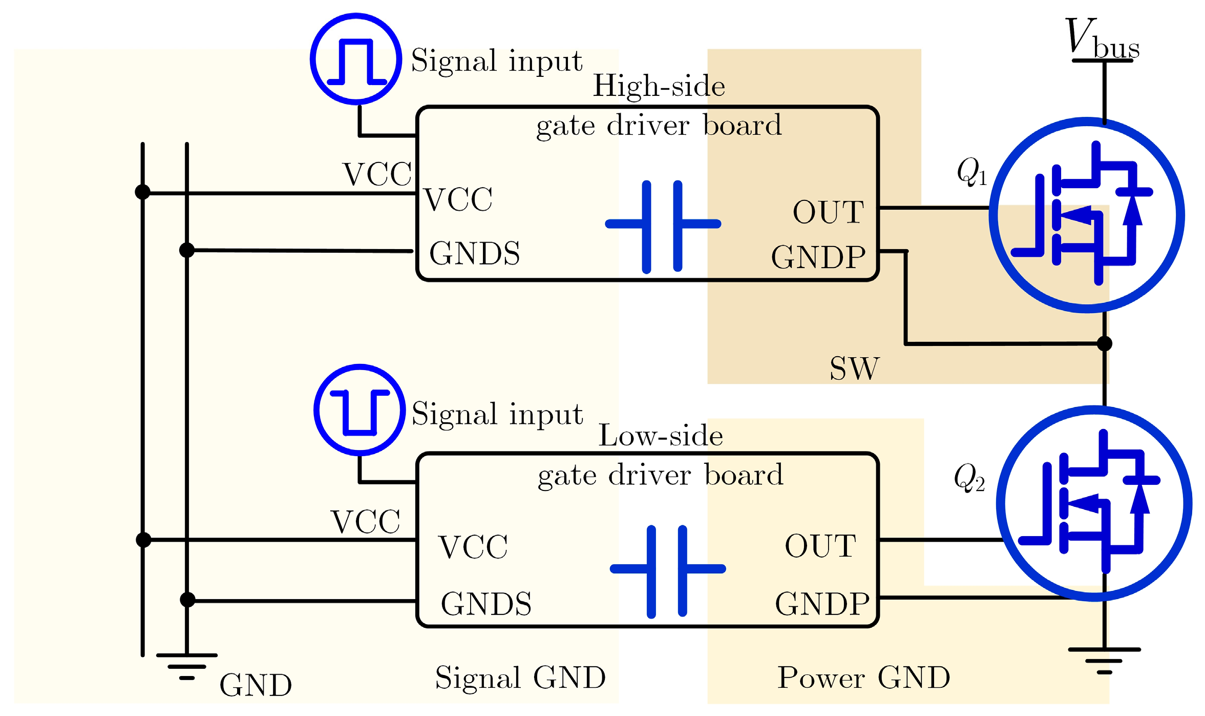
Figure 1. Structure of the driver circuit for the half-bridge submodule.
Energies 18 06083 g001
Figure 2. Conduction path of common-mode current.
Energies 18 06083 g002
Figure 3. Architecture of the high-side driver circuit.
Energies 18 06083 g003
Figure 4. Network model of the high-side driver circuit.
Energies 18 06083 g004
Figure 5. Simplification of the power supply branch.
Energies 18 06083 g005
Figure 6. Simplification of the decoupling capacitor.
Energies 18 06083 g006
Figure 7. Result of the simplification of the power supply branch.
Energies 18 06083 g007
Figure 8. Simplified network of the driver circuit.
Energies 18 06083 g008
Figure 9. Network model of the common-mode interference loop in the half-bridge submodule.
Energies 18 06083 g009
Figure 10. The process of finite element simulation.
Energies 18 06083 g010
Figure 11. Comparison of commercial isolated power supply.
Energies 18 06083 g011
Figure 12. Simulation setup of the excitation source UCM.
Energies 18 06083 g012
Figure 13. Time-domain and frequency-domain analysis of common-mode current.
Energies 18 06083 g013
Figure 14. Comparison of currents in signal control branches.
Energies 18 06083 g014
Figure 15. Influence of RLC on common-mode current.
Energies 18 06083 g015
Figure 16. Comparison of commercial isolated power supplies.
Energies 18 06083 g016
Figure 17. Configuration of the driver circuit.
Energies 18 06083 g017
Figure 18. Capacitor design scheme.
Energies 18 06083 g018
Figure 19. Diagram of 3D integration.
Energies 18 06083 g019
Figure 20. Prototype of power submodule.
Energies 18 06083 g020
Figure 21. Test platform for high-voltage SiC submodule.
Energies 18 06083 g021
Figure 22. Simulation waveform of the buck test.
Energies 18 06083 g022
Figure 23. Test waveform of the buck test.
Energies 18 06083 g023
Figure 24. Thermal imaging of buck test.
Energies 18 06083 g024
Figure 25. Experimental result of the double pulse test.
Energies 18 06083 g025
Figure 26. Measured waveform of common-mode current.
Energies 18 06083 g026
Table 1. Physical meaning of parasitic parameters.
ParameterPhysical MeaningParameterPhysical Meaning
Lp1Input parasitic inductor of IPSLsParasitic inductor between fiber optic and GD IC
Lp2Input parasitic inductor of DC/DC moduleLgParasitic inductor between GD IC and the source of MOSFET
Lp3Input parasitic inductor of Second IPSC1Coupling capacitor of IPS
Lp4Parasitic inductor of fiber optic conversion circuitC2Coupling capacitor of Second IPS
Lp5Output parasitic inductor of GD ICC3Coupling capacitor of the GD IC
Lp6Input parasitic inductor of GD ICRgParasitic resistance between GD IC and the source of MOSFET
Table 2. Typical values corresponding to the capacitance parameters.
ParametersSeriesValue (pF)
C1NXE1S0505MC-R133
C21ED332xMC12N1.4
C3NXE1S0505MC-R133
Table 3. Extraction results of the parasitic parameter.
ParameterValueParameterValue
Lp13.73 nHLp65.9 nH
Lp211.35 nHLs7.7 nH
Lp33.31 nHLg26.8 nH
Lp48.18 nHRg0.36 ohm
Lp54.62 nH
Table 4. Comparison of commercial 3.3 kV SiC MOSFET.
SeriesG2R1000MT33JMSC400SMA330B4G2R120MT33J
CompanyGeneSiC (Chantilly, VA, USA)Microchip (Chandler, AZ, USA)GeneSiC (Chantilly, VA, USA)
ID3 A11 A35 A
Qg21 nC37 nC145 nC
RDS(on)1000 mΩ400 mΩ120 mΩ
Cost$18.69$32.11$92.99
Table 5. Comparison of three capacitor design schemes.
1st Option2nd Option3rd Option
Volt. [kV]3.03.03.0
Cap. [μF]105.0200.060.0
Cur. [A]57.080.0101.1
ESL [nH]110.0100.012.6
ESR [mΩ]6.01.62.1
Vol [L]2.33.31.8
Table 6. Comparison of common-mode current suppression among different methods.
[1][2][3]This Work
Test voltage 1.1 kV5.0 kV6.8 kV0.4 kV
dv/dt65.4 kV/μs65 kV/μs81 kV/μs20 kV/μs
The method used in paperCustomized isolated power supplyCustomized isolated power supplyCustomized isolated power supply and shielding techniquesThe proposed method and commercial power supplies
Measured CM current on gate driver426 mA471 mA130 mA68 mA
Disclaimer/Publisher’s Note: The statements, opinions and data contained in all publications are solely those of the individual author(s) and contributor(s) and not of MDPI and/or the editor(s). MDPI and/or the editor(s) disclaim responsibility for any injury to people or property resulting from any ideas, methods, instructions or products referred to in the content.