Review

GaN Electric Vehicle Systems—A Comparative Review

by
Ifeoluwa Ayomide Adeloye
1,
Indranil Bhattacharya
2,*,
Ernest Ozoemela Ezugwu
1 and
Mary Vinolisha Antony Dhason
1
1
Department of Electrical and Computer Engineering, Tennessee Technological University, Cookeville, TN 38505, USA
2
Department of Electrical and Computer Engineering, Binghamton University, 4400 Vestal Pkwy E, Binghamton, NY 13902, USA
*
Author to whom correspondence should be addressed.
Energies 2025, 18(22), 6020; https://doi.org/10.3390/en18226020
Submission received: 10 October 2025 / Revised: 11 November 2025 / Accepted: 13 November 2025 / Published: 17 November 2025
(This article belongs to the Section E: Electric Vehicles)

Abstract

Gallium nitride (GaN) devices are gaining rapid adoption in electric vehicle (EV) power electronics because of their high switching speed, efficiency, and passive size reduction. The remaining gaps concern reliability across real drive cycles, integration with vehicle-level thermal subsystems, and scalability to high-voltage platforms. This review addresses these gaps by synthesizing experimental reports and automotive case studies from 2019 to 2025. We examine reliability through junction stress and derating maps derived from urban/highway duty profiles and temperature extremes, and we link device hot-spots to thermal pathways (TIMs, spreaders, liquid/air cooling) within the EV thermal budget. We then compare GaN-based onboard chargers (OBCs), DC–DC stages (LLC/CLLC/DAB), traction inverters, and EMI strategies against Si/SiC baselines. Results indicate OBC efficiencies of 96–98% at 100–500 kHz, with 30–60% passive reduction; inverter efficiencies > 98% on 400 V platforms; and strong potential for GaN paired with Vienna or T-type rectifiers in 800 V charging, while >900 V traction remains largely SiC-led. We conclude with a topology-selection framework that balances switching and conduction losses, gate-driver complexity, and EMI, plus a roadmap toward EMI-compliant MHz operation and data-driven reliability evaluation.

1. Introduction

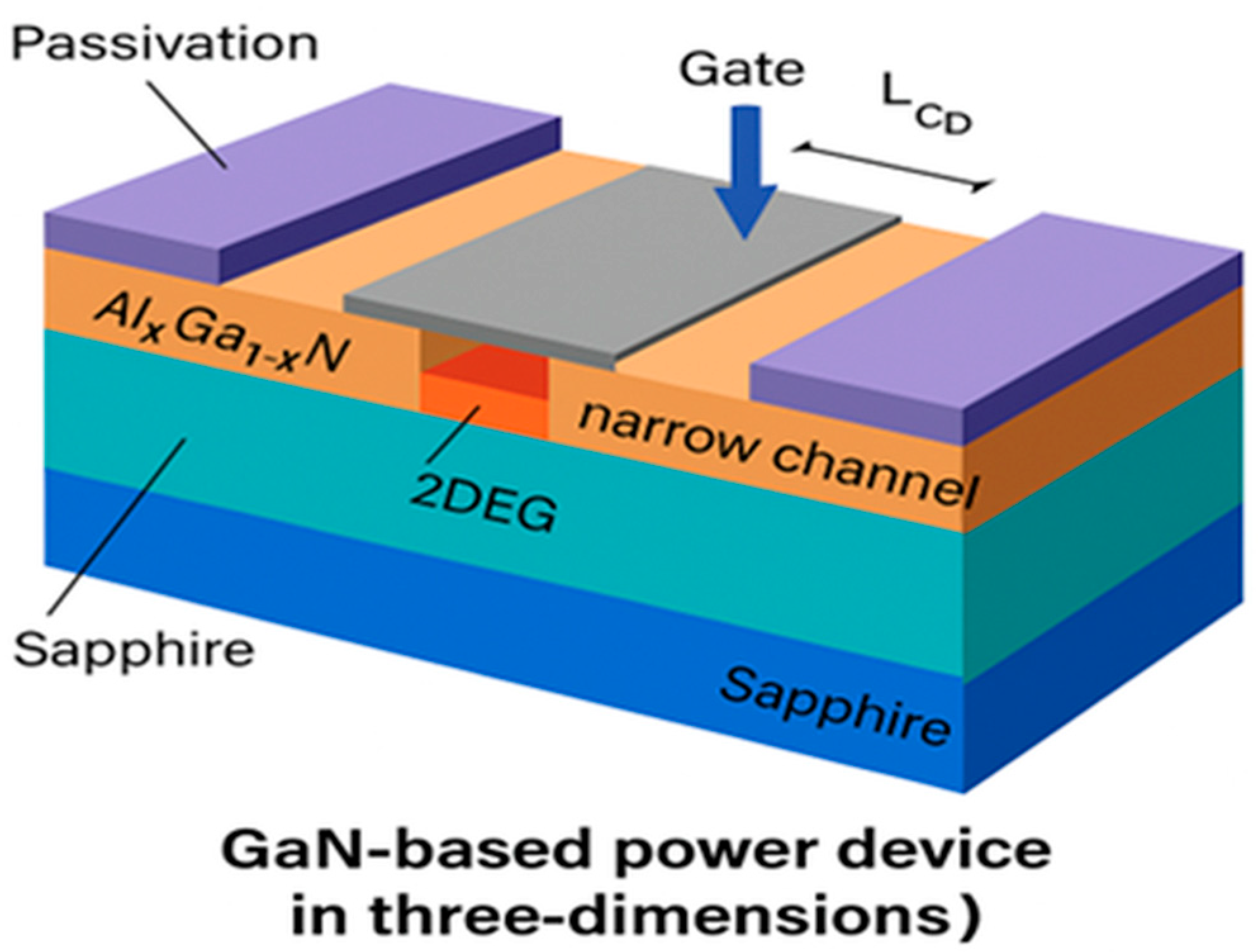
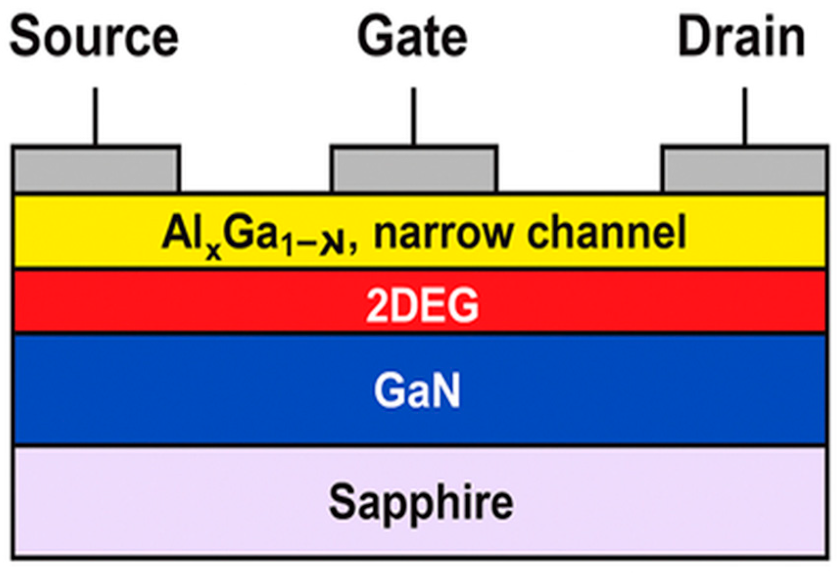
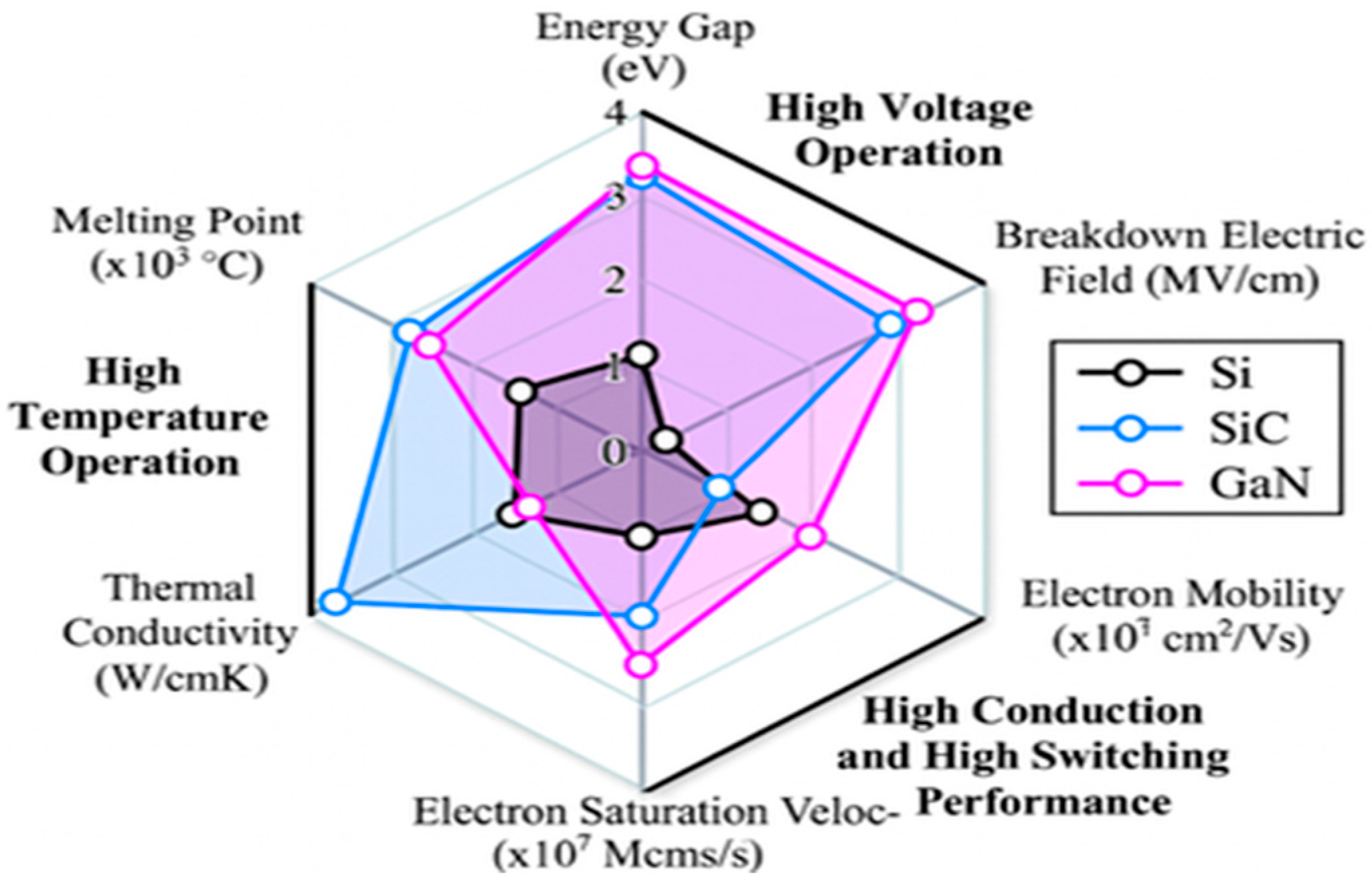
Electric vehicles (EVs) are reshaping modern transportation, creating demand for compact, efficient, and reliable power conversion systems. Conventional silicon-based devices are increasingly constrained in switching frequency, voltage stress, and thermal robustness, limiting their suitability for next-generation EV requirements [1,2]. Wide-bandgap (WBG) semiconductors, notably gallium nitride (GaN), offer a wide bandgap of 3.4 eV, high electron mobility, and negligible reverse recovery, enabling faster switching, reduced passive size, and higher efficiency compared with silicon and even silicon carbide (SiC) [3,4,5]. These features have accelerated GaN’s adoption in critical EV subsystems such as on-board chargers (OBCs), DC–DC converters, traction inverters, and EMI filters [6,7]. At the material and device level, GaN’s wurtzite lattice supports high breakdown fields (Figure 1), while the AlGaN/GaN heterostructure forms a high-mobility two-dimensional electron gas (2DEG) channel used in practical HEMTs (Figure 2 and Figure 3) [3,4,5].
Several recent reviews have summarized GaN’s role in electric mobility. Rahman et al. [8] provided a broad survey of WBG devices, integrating material physics, subsystem applications, and reliability. Similarly, Soomro et al. [9] offered a forward-looking analysis of GaN in traction drives. While informative, these surveys often combine GaN with SiC or focus on selected subsystems, leaving open questions about GaN’s role across the entire EV power chain. Furthermore, the existing literature seldom addresses reliability under real-world drive cycles, the interaction between localized GaN heating and vehicle-level thermal budgets, or systematic guidance for scaling converters in 400 V and 800 V battery platforms, where SiC devices still dominate traction inverters [10,11,12].
This paper addresses these gaps by presenting a subsystem-oriented review that compares GaN implementations in OBCs, DC–DC converters, traction inverters, and EMI filters, while developing a reliability- and topology-aware framework for evaluating trade-offs. In particular, we synthesize experimental reports and case studies from 2019 to 2025 to (i) link device-level heating to vehicle thermal management strategies [13,14,15], (ii) assess scaling feasibility for 400/800 V EV architectures [10,16], and (iii) provide a comparative basis for selecting topologies such as Vienna vs. T-type rectifiers in high-power OBCs [17,18]. By correlating device physics with system-level design, this review delivers differentiated insights beyond prior surveys and offers practical guidance for GaN integration in EV powertrains [19].
Organization of the paper: The remainder is structured into six sections plus the conclusion. Section 2 consolidates GaN material/device background and the review methodology (2019–2025 scope, databases, inclusion/exclusion, and evaluation metrics). Section 3 examines reliability under real drive cycles and links device-level heating to the vehicle thermal budget. Section 4 reviews GaN-based AC–DC front ends for 400 V/800 V platforms, comparing Vienna and T-type NPC choices. Section 5 covers the DC–DC stages (LLC/CLLC/DAB), emphasizing ZVS/ZCS and scaling trade-offs. Section 6 treats EMI and compliance, including a dual-LISN DM/CM workflow and a practical topology-selection framework (Pareto maps/decision matrix). Section 7 concludes with key findings and a roadmap.

2. GaN Material/Device Background and Review Methodology

Gallium nitride (GaN) crystallizes in the wurtzite structure and, with an AlGaN barrier, forms a high-mobility two-dimensional electron gas (2DEG) that enables fast, low-loss switching in power HEMTs. The device’s physical traits that are most relevant to EV converters—negligible reverse-recovery charge, low C o s s and gate charge, and a high breakdown electric field E c r i t —translate into higher practical switching frequency, reduced magnetic/passive volume, and efficiency that is competitive with Si and, in many 400 V cases, even SiC [3,4,5]. In EV subsystems (OBCs, HV–LV/HV–HV DC–DC converters, traction inverters, EMI filters), enhancement mode (p-GaN gate) HEMTs and cascade GaN are the dominant options: both minimize stored charge but require careful d v d t control through a gate-loop design and layout to avoid overshoot, ringing, and false turn-on.
Figure 1, Figure 2 and Figure 3 illustrate the crystal structure and typical AlGaN/GaN HEMT cross-sections used throughout this review [3,4,5]. Figure 4 compares Si/SiC/GaN device properties (bandgap, E c r i t , mobility, specific R D S ( o n ) , Q r r , and C o s s ) to anchor later platform (400 V/800 V) and topology comparisons. Table 1 lists the key parameters we reference repeatedly in Section 3, Section 4, Section 5 and Section 6.
High-slew operation makes layout/packaging and thermal paths first-order EV design variables. Minimizing common-source inductance (Kelvin-source returns, compact current loops, laminated buses) and managing Miller coupling (clamps or controlled slew) preserve switching benefits and contain EMI. Because GaN pushes frequency upward, junction-to-ambient paths (TIMs, spreaders, cold plates) must be co-optimized with magnetics and EMI, so device T j remains within automotive limits across urban/highway/temperature-extreme mission profiles—this linkage is developed further in Section 3. Recent 400 V OBC prototypes with GaN demonstrate the frequency/efficiency/power-density advantages that are now achievable, and the packaging/thermal practices needed for robust operation [20,21,22].
In practical GaN power devices, the drain-to-source resistance cannot be treated as a fixed static value because transient charge-trapping phenomena introduce a dynamic component [23]. The apparent resistance during switching can be expressed as
R D S ( O N ) d y n ( t ) = R D S ( O N ) s t a t [ 1 + Δ t r a p   ( V D S , o f f ,   T j ,   T o f f ) ] ,
where R D S ( O N ) s t a t is the steady-state resistance, and Δ t r a p is a bias- and temperature-dependent correction term associated with electron trapping in surface and buffer states during the preceding off-state [24]. When a GaN HEMT is subjected to high V D S , o f f , off and elevated junction temperature T j electrons are captured in deep traps at the GaN/AlGaN interface or buffer layer [25]. Upon the next turn-on, these trapped charges temporarily reduce channel conductivity, leading to the well-known current-collapse phenomenon and an elevated dynamic, R D S ( O N ) d y n . The transient evolution of this resistance can be modeled as
Δ t r a p ( t ) = i α i   ( 1 e t τ i ) ,
where each τ i represents a characteristic emission time constant for a specific trap population, and α i denotes its relative occupancy [26]. This time-dependent formulation captures the slow recovery of the channel as trapped carriers are released between switching cycles. The total conduction loss during dynamic operation therefore increases by
p C o n d d y n = I D , r m s 2   R D S ( O N ) d y n
Because the trapping process depends strongly on the off-state dwell time T o f f and drain bias V D S , o f f , accurate characterization requires pulsed double-pulse testing (DPPT) or on-wafer dynamic R O N measurement systems that replicate realistic converter operating sequences [27].
Recent experimental work introduced a reconfigurable test setup that is capable of emulating variable blocking voltages, current slopes, and duty ratios, enabling the extraction of R D S ( O N ) d y n (t) under automotive-grade conditions (Alemanno et al., 2023 [28]). Such dynamic measurement remains an active research area because it bridges material-level trapping physics with circuit-level conduction-loss modeling, which is essential for reliability-aware GaN design in EV converters [29].
To keep comparisons fair across heterogeneous reports, this review considers EV-relevant works (2019–2025) that publish measurable electrical, thermal, and EMI outcomes across the OBC, DC–DC, inverter, and EMI-filter stages [30]. We track efficiency at/near the rated load; switching frequency and mode (soft vs. hard); reported power density; thermal headroom (peak T j and cooling architecture); EMI margin to automotive limits using LISN-based methods; and reliability indicators (mission-profile mapping, dynamic R D S ( o n ) , power-cycling/HTOL notes). For EMI method references, we use CISPR-25 [31] and widely used practitioner notes clarifying voltage vs. current probe approaches. For three-phase AC/DC front ends on 400/800 V platforms, comparative studies of Vienna and T-type NPC rectifiers consistently show high efficiency, with different trade-offs in bidirectionality, control, and device count; these inform the selection framework developed in Section 4, Section 5 and Section 6.

3. Reliability Under Real Drive Cycles and Linkage to the Vehicle Thermal Budget

Reliable GaN deployment in EVs depends on how converter stress accumulates over real drive cycles and how that stress is absorbed by the vehicle thermal subsystem. At the device level, GaN’s negligible reverse-recovery charge and low stored charge reduce switching loss versus Si and often SiC, but fast edges concentrate stress into short intervals that are sensitive to parasites and temperature. Practical degradation channels include p-GaN gate wear-out, trapping and dynamic R D S ( o n ) , current collapse, hot-electron effects at high field, and thermo-mechanical fatigue in interconnects and die-attach [32,33,34], whose evolution under drive cycle stress directly couples to the charge-trapping mechanisms and measurement challenges outlined in Section 2. Accurate lifetime prediction therefore requires profile-aware screening of dynamic R D S ( o n ) using pulsed or on-wafer characterization to capture trap-induced drift across blocking intervals.
Recent wafer-level characterization studies have underscored these challenges by demonstrating that even controlled dynamic R D S ( O N ) measurements are strongly influenced by the parasitic impedance of probe fixtures and the thermal time constants of high-voltage dies. In particular, Alemanno et al. [28] presented a reconfigurable on-wafer setup that was capable of emulating realistic blocking and conduction intervals, revealing how temperature rise and trap filling alter the measured on-resistance. Such experimental frameworks provide valuable calibration data for correlating laboratory switching stress with the in-vehicle thermal budget and for refining lifetime prediction under mission-profile conditions.
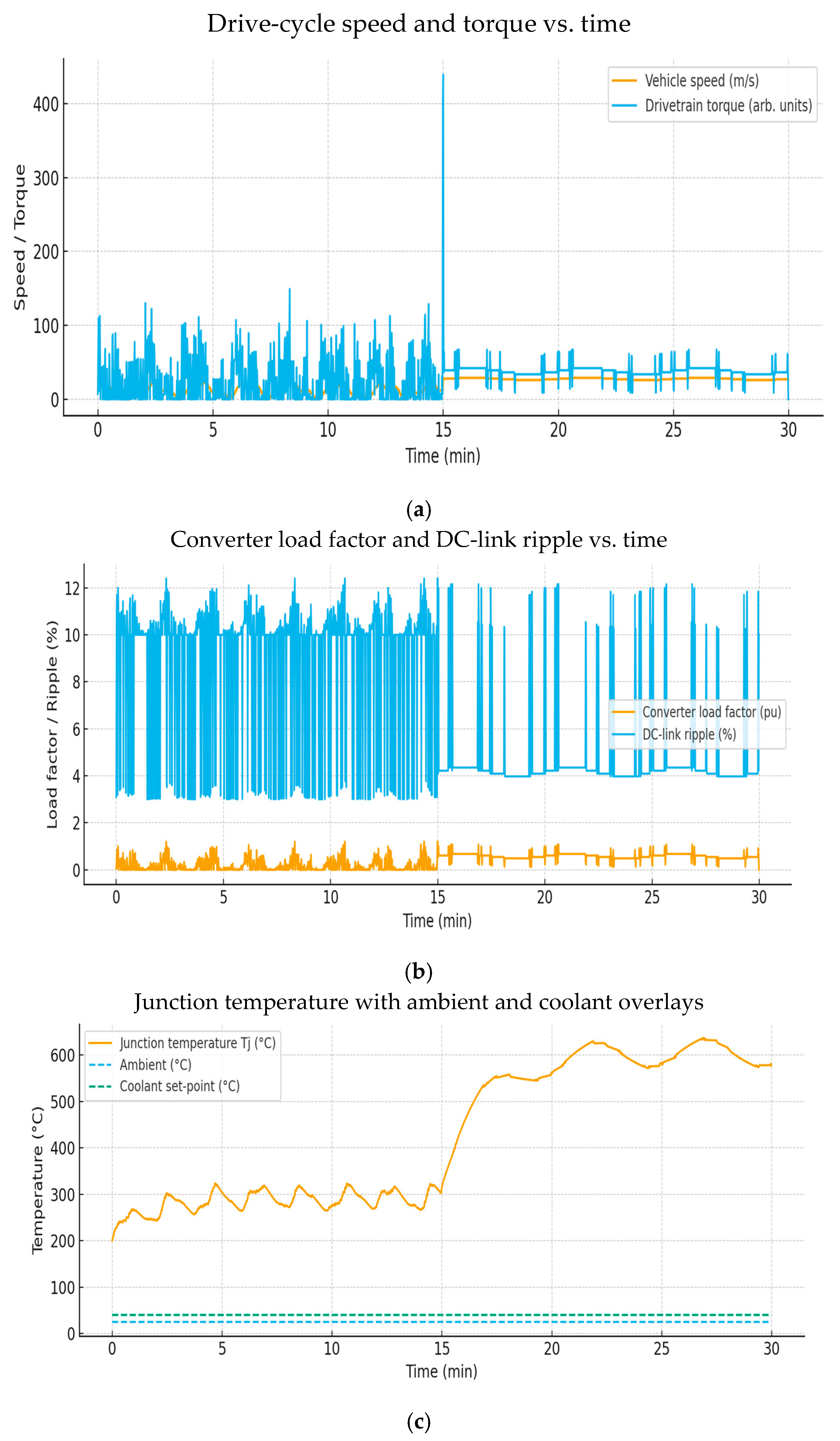
Mission profile matters: urban cycles (frequent transients) create many modest Δ T j events, while highway cycles create fewer but larger thermal excursions. Consequently, lifetime predictions and derating must be built around profile-aware stress metrics, rather than single worst-case points [35]. As depicted in Figure 5a–c, we map the drive cycle to electrical and thermal trajectories.
To translate vehicle duty into converter stress, we map speed/torque and charging events to electrical loading (DC-link ripple, phase currents, switching conditions). With measured thermal impedances ( R θ j c ,   R θ c a ) and coolant set-points, this yields a junction-temperature trajectory T j (t). Those trajectories feed three lifetime surrogates:
(i)
Arrhenius-type acceleration for steady high-temperature wear mechanisms;
(ii)
Coffin–Manson accumulation for thermo-mechanical cycling;
(iii)
Screening of dynamic R D S ( O N ) as a proxy for trapping-induced conduction-loss drift under realistic blocking/rest intervals. JEDEC-style dynamic R D S ( O N ) procedures and double-pulse tests make these metrics comparable across reports [36,37]. Figure 5 illustrates the pipeline from duty cycle → electrical load → T j ( t ) .
The thermal budget constraint that drives the derating logic is
T j = T c o o l , i n + Q l o s s   ( R θ j c + R θ c a )   T j , m a x H t h
here T c o o l , i n is the coolant inlet temperature, Q l o s s is the total device heat at the operating point, R θ j c and R θ c a are the junction-to-case and case-to-ambient (or cold-plate) thermal impedances, T j , m a x is the allowed junction limit, and H t h . There is a guard margin for ambient swings, coolant derating, and sensor tolerance. In practical converter assemblies, the steady-state form of (4) may underestimate localized junction heating. Factors such as voids in the die attach, solder fatigue, and coolant-flow nonuniformity increase the effective thermal impedance Z t h . over time. Reliability prediction should therefore include transient thermal-impedance data and temperature-dependent material properties to capture these cumulative effects.
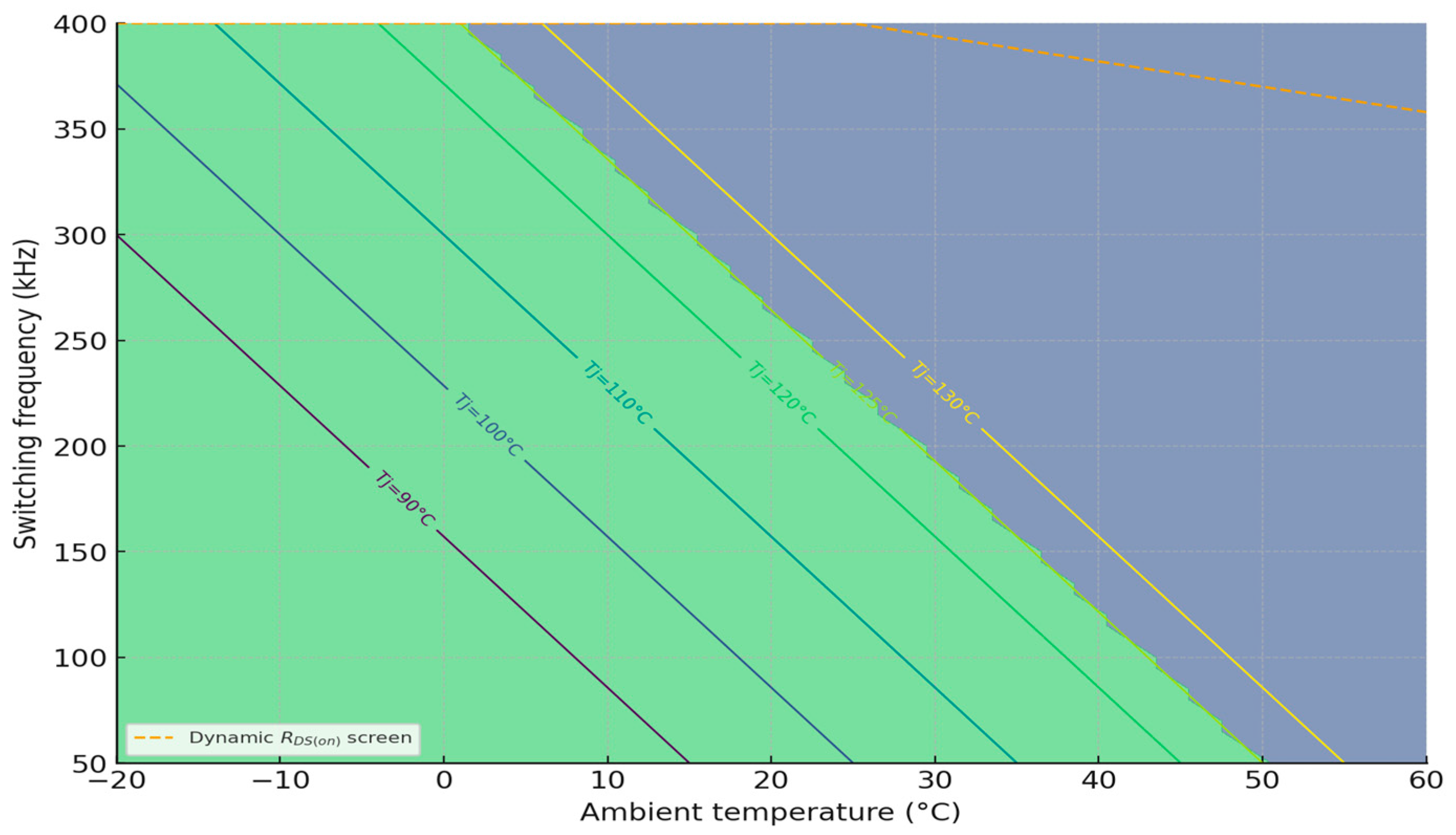
Because GaN enables a higher switching frequency, magnetics and EMI filters shrink but heat-flux density rises; spreaders and cold-plates must therefore be co-optimized with gate-loop and layout choices that cap overshoot, ringing, and d v d t [38,39]. In practice, designers sweep frequency versus loss and coolant set-point to generate a reliability-aware derating map that defines safe operating regions over ambient, load factor, and vehicle speed. As summarized in Figure 6, the safe region is bounded by the T j limit (e.g., 125 °C with a margin) and a temperature-dependent dynamic R D S ( o n ) screen [40].
Measurement and screening close the loop. Double-pulse tests with controlled blocking intervals expose dynamic R ( o n ) ; HTOL/HV off-state campaigns track gate wear-out; and power-cycling quantifies attach/wire fatigue across representative Δ T j bands, while LISN-based DM/CM scans verify conducted-EMI margins for the chosen operating point [41,42,43,44]. Used properly, these datasets enable guard-banded windows that meet multi-year automotive targets without sacrificing the frequency advantages that are central to GaN. The resulting profile-aware derating approach is as follows: cap T j (with margin), limit d v d t via driver and layout to reduce EMI-linked stress, and validate with LISN-based DM/CM scans so thermal and EMI design are closed concurrently, not sequentially.
The derating map constrains not only the allowable junction temperature but also the dissipation available for snubbers and EMI networks. Since filter and snubber losses are concentrated at a high frequency, the chosen switching spectrum and any edge-shaping that improves EMI must be verified against the same thermal budget used to cap T j . Section 6 quantifies the required DM/CM attenuation and shows how topology and edge control can meet those limits without violating the reliability envelope defined here.

4. GaN-Based AC–DC Front Ends for 400 V/800 V EV Platforms

GaN enables a higher switching frequency and a much lower switching charge than Si/SiC, which is especially valuable at the AC–DC front end of the OBC, where grid power quality (PFC), efficiency, and power density are tightly constrained [45,46,47]. Throughout this section, key converter acronyms are defined for convenience: totem-pole power factor correction (TP-PFC), neutral-point-clamped (NPC), on-board charger (OBC), and electromagnetic interference (EMI).
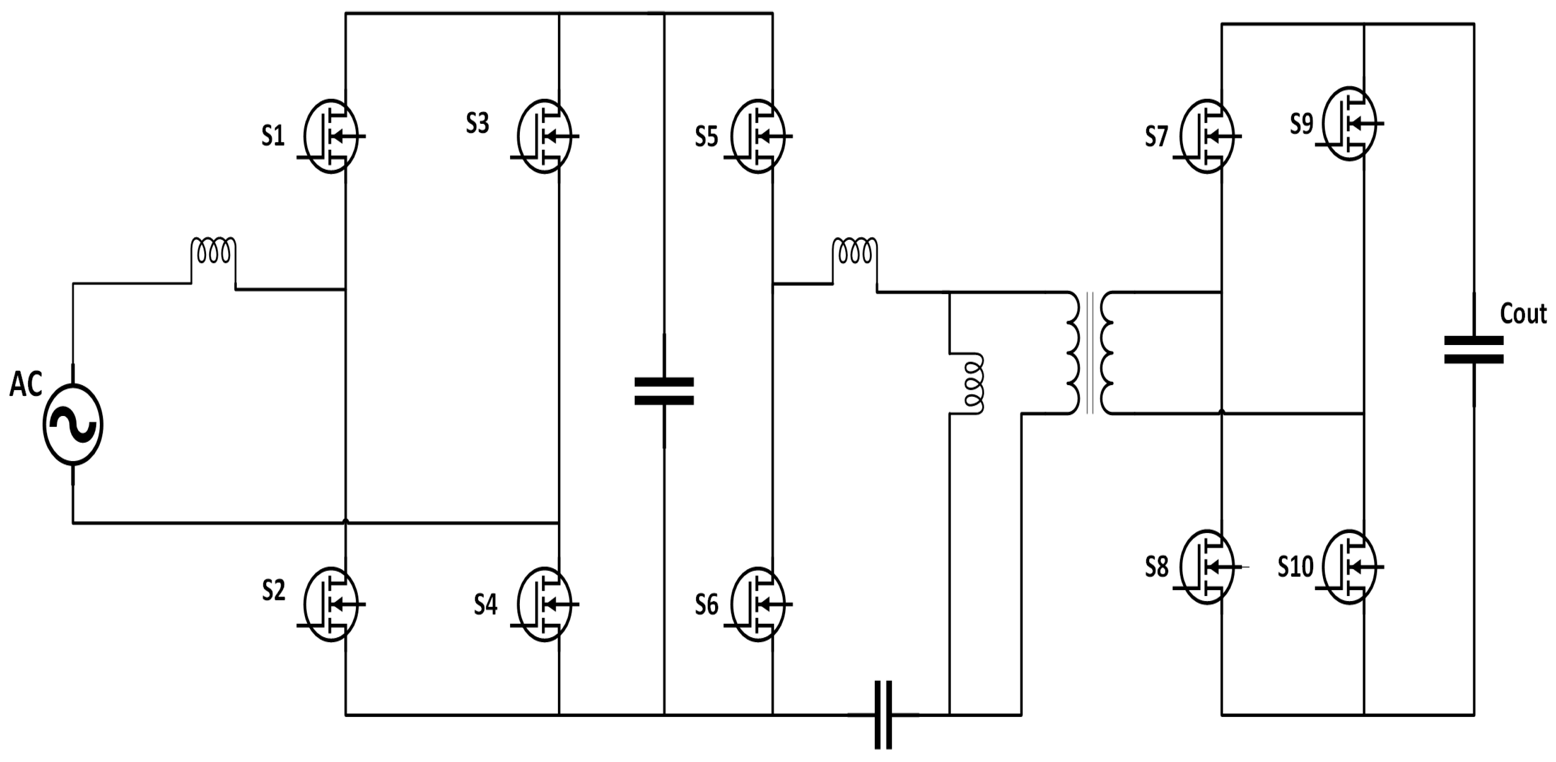
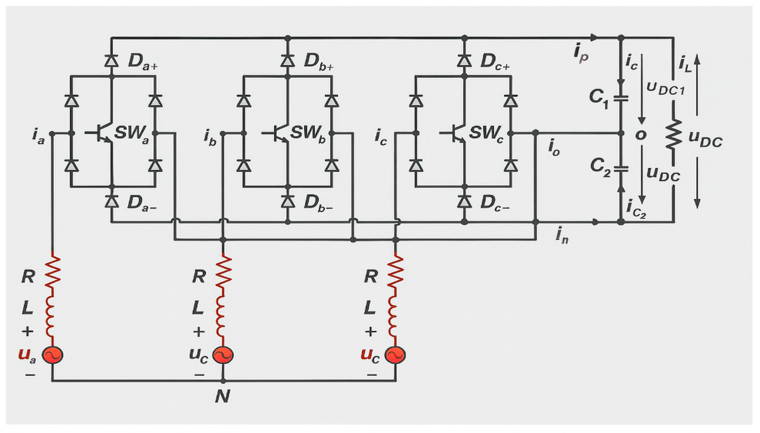
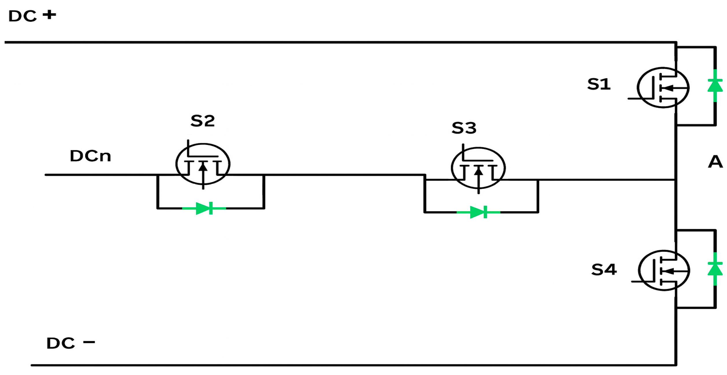
For single-phase charging, the bridgeless totem-pole PFC (TP-PFC), followed by a resonant DC–DC stage (LLC/CLLC/DAB), is now a mainstream GaN solution, as depicted in Figure 7. For three-phase charging, GaN favors three-level (3L) rectifiers that halve device voltage stress and reduce d v d t : the Vienna rectifier (unidirectional by default; Figure 8) and the T-type neutral-point-clamped (NPC) rectifier (naturally bidirectional V2G/V2H; v 9). These options respond directly to 400/800 V scaling and the Vienna vs. T-type trade-offs [48,49,50], while providing a quantitative basis for the topology selection [51].
  • Single-phase TP-PFC + resonant DC–DC (LLC/CLLC/DAB)
Unity-power-factor (UPF) control is achieved by shaping the input current reference proportionally to the instantaneous mains voltage
i r e f ( t ) = 2 P o u t V g ,       r m s 2   v g   ( t ) ,
with current mode or predictive control maintaining i r e f (t) = k v i n (t), where k is set by the desired input conductance i (t) ≈ i r e f (t) [52]. The resonant stage uses the standard definitions [53]. Where L r and C r are the tank elements, R L is the reflected load, and ω r = 2π f r .
f r = 1 2   π   L r   C r ,   Q = R L ω r   L r ,
ZVS is obtained when the tank energy during dead time exceeds the energy to commutate device capacitances [54]:
1 2   L e q   i L 2     =   k 1 2   C o s s ,       k   V d s ,       k 2
In this GaN-based arrangement, switching transitions are fast and largely capacitive, so E S W C e q     V 2 is minimized; magnetics and EMI filters shrink, improving density [55].
Equation (7) expresses the ideal ZVS boundary, assuming perfectly linear capacitances and negligible loop inductance. In hardware, parasitic inductance and the non-linear voltage dependence of C o s s   ( V ) reduce the stored energy available for commutation, while the gate-driver delay and dead time variation shift the actual ZVS point. Time-domain simulation or double-pulse verification is required to confirm full-range soft switching.
b.
Three-phase front ends—Vienna vs. T-type (Figure 8 and Figure 9).
For 400/800 V buses, GaN benefits from 3L rectifiers because device voltage stress is halved:
V d s ,       m a x   ( 3 L )   V d c 2   vs .   V d s ,       m a x   ( 2 L )   V d c
Current shaping for unity PF per phase is
i a   * ( t ) = k   V a ( t ) ,   k = 2   P o u t 3   V p h ,       r m s 2 ,
with analogous expressions for b and c. In both 3L topologies, the split-DC link requires neutral-point balance; a small duty-offset δ (or redundant state selection) regulates the capacitor voltages V c 1   V c 2   :
d d t ( V c 1     V c 2   )   =   i N   ( δ ) C ,
where i N is the neutral current modulated by δ [56]. Building on (8)–(10), the loss and EMI implications of three-level (3L) front ends can be summarized as follows.
  • Switching-loss scaling (3L vs. 2L)
For hard transitions, the energy per event scales with the square of the device voltage. Because a 3L leg limits device stress to ≈ V d c   2 , the per-transition energy is approximately quartered:
E S W   ( 3 L )   C e q ( V d c   2 ) 2 =   1 4 C e q V d c   2
This reduction, together with GaN’s inherently low output capacitance, enables operation at higher switching frequencies f s and smaller passives [57], as depicted in Figure 8 (Vienna) and Figure 9 (T-type). Consequently, a 3L leg achieves roughly one-fourth of the switching energy compared with a conventional two-level leg.
The proportionality in (11) neglects the overlap current and dynamic output–capacitance variation. Under high d v d t or mismatched dead times, the effective E S W deviates from the ideal quarter-scaling. Experimental calibration using measured R D S O N T and loop inductance L l o o p is needed for accurate loss estimation.
  • Conduction loss composition. For phase RMS current I r m s ,
P c o n d = a c t i v e   p a t h         I   r m s 2   R D S   ( o n ) + d i o d e s V f   I a v g ,
So, Vienna (with diodes in some current paths) incurs an additional V f   I a v g term, whereas the T-type is fully active (no diode drops) but uses more switches and drivers. Which term dominates depends on the operating point and device choices [58].
  • Common mode d v d t and EMI
The displacement current to the chassis is i C M C p a r   d v d t . Because a 3L transition halves Δ   V and typically reduces d v d t for a given edge time, the Vienna and T-type generally relax conducted EMI filtering compared with two-level legs—consistent with LISN-based methods seen later in Section 6—see Figure 8 and Figure 9 for the commutation states that set Δ   V [59,60].
Topology implications and platform fit.
  • Vienna rectifier (Figure 8)—Unidirectional by default, simple modulation, very low switching loss from (8), and device stress limited by (5). It is a strong choice when peak efficiency and simplicity are priorities and vehicle-to-grid (V2G) is not required.
  • T-type NPC (Figure 9)—Naturally bidirectional (V2G/V2H), with the same 3L stress relief. It requires neutral-point control per (7), careful commutation sequencing, and a higher driver/channel count.
For 400 V buses (650 V GaN), both 3L options comfortably reach f s ≈ 100–300 kHz with high efficiency and manageable EMI. For 800 V buses, the 3L front ends allow the reuse of 650/700/900 V GaN while keeping V d s in a comfortable range; direct two-level GaN at 800 V is usually limited to series-stacked solutions with active sharing [61,62].
c.
Quantitative selection rubric
A pragmatic way to balance losses, EMI, and implementation effort is
J = α   P s w + β   P c o n d + γ   ϕ E M I + ζ   C d r v
where ϕ E M I reflects driver/channel count and C d r v reflects driver/channel count neutral-point control effort. Minimizing J over candidate topologies and switching frequencies f s , subject to thermal constraints from Section 3, yields the recommended operating point [63].
Stage efficiency accounting. For all three front ends (TP-PFC, Vienna, T-type), the overall conversion efficiency is
η = P s w P o u t   +   P s w +   P c o n d   +     P c u   +   P g d r v ,
with P s w and P c o n d from (13) and (14), and magnetic losses from Steinmetz/AC-resistance models at the chosen f s , and P g d r v , set by gate charge and switching frequency [64]. The schematic and current paths referenced in (10)–(14) are shown in Figure 8 (Vienna) and Figure 9 (T-type).
Applying (13)–(16) to the three-level front end shows a crossover region in which the Vienna rectifier attains a small but measurable efficiency edge at a give f s due to diode-assisted commutation and reduced driver count, whereas the T-type NPC becomes preferable when bidirectionality and neutral-point control are required. In both cases, halved device-node swing in (8) reduces CM injection, easing the EMI margin requirement ΔE in Section 6. The selection boundary can thus be parameterized by { P r a t e d , f s , I R M S , Δ v n o d e , C p a r , C e q }, with complexity cost C (Equation (13)) tipping the decision when V2G/V2H is mandated.
d.
Gate driver and parasitic control for GaN AC–DC legs (TP-PFC, Vienna, T-type).
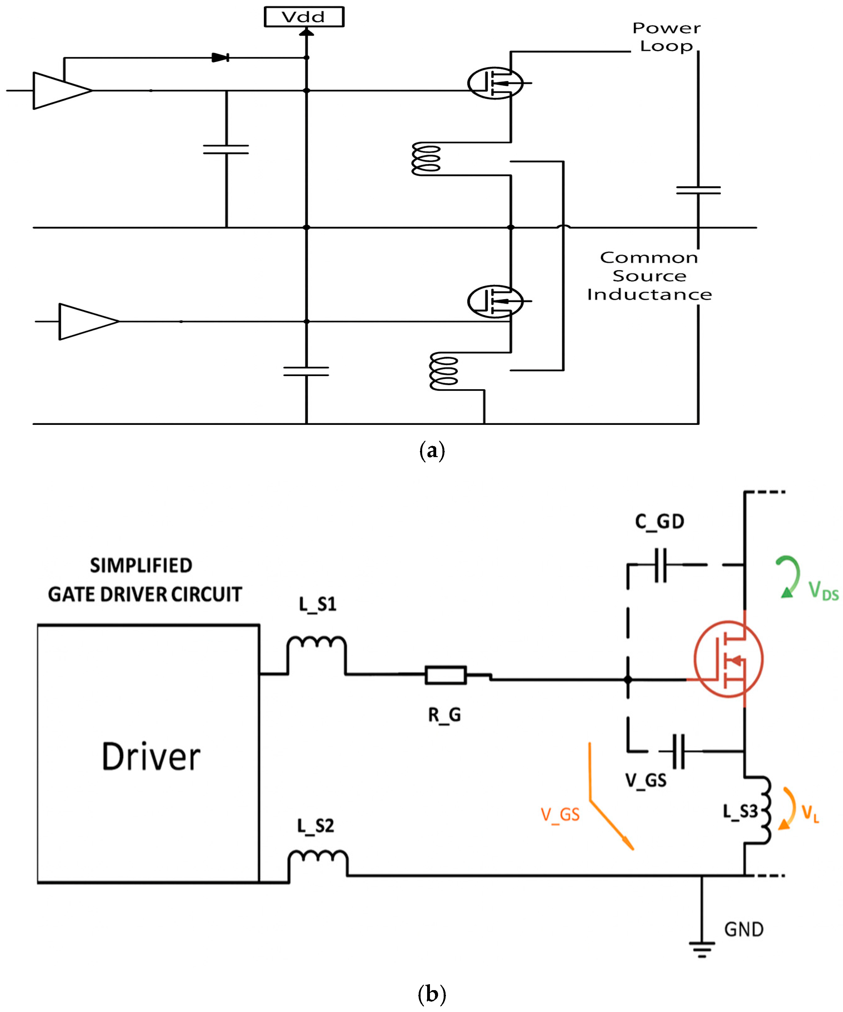
At GaN edge rates, the gate loop and power loop behave as coupled RF networks, so driver choice and physical layout directly determine loss, overshoot, and EMI in the AC–DC front ends. The critical parasites are the common-source inductance (CSI) in the gate return and the Miller coupling C g d from the switching node to the gate. The gate perturbation from the commutation current is
V G S ,       b o u n c e   L C S I   d i D d t
so even L C S I = 2–10  nH, with d i d t of tens of A/ns, can inject several hundred millivolts on the gate, unless a Kelvin-source return is used and the driver is placed within a few millimeters of the devices [65,66]. During fast drain transitions, the Miller current into the off device is
i M i l l e r   C g d   d V D d t ,   Δ V G S ,       o f f   C g d C g s + C s t r a y   Δ V D
which can cause a false turn-on if the off-path is weak. Immunity is achieved with a strong turn-off path (low R g ,   o f f ), an active Miller clamp (engaged when V G S falls below a clamp threshold), and—only where permitted by the datasheet—a slight negative off-bias to increase the margin to V t h . The resulting off-state condition may be checked by
V t h ,       o f f   V t h ,       m i n ( V t h ,       b o u n c e + Δ V G S ,       o f f ) .
Ref. [67] shows power-loop parasitic set overshoot and ringing, impacting EMI and snubber loss. Minimizing the commutation triangle (high-side FET–low-side FET–DC-link MLCC), routing the gate loop as a tight differential pair to the Kelvin-source, and separating gate and power returns limit both L l o o p and C p a r [68]. These measures are especially effective in three-level Vienna and T-type rectifiers, where reduced device swing already halves Δv relative to two-level legs, easing CM injection and filter burden.
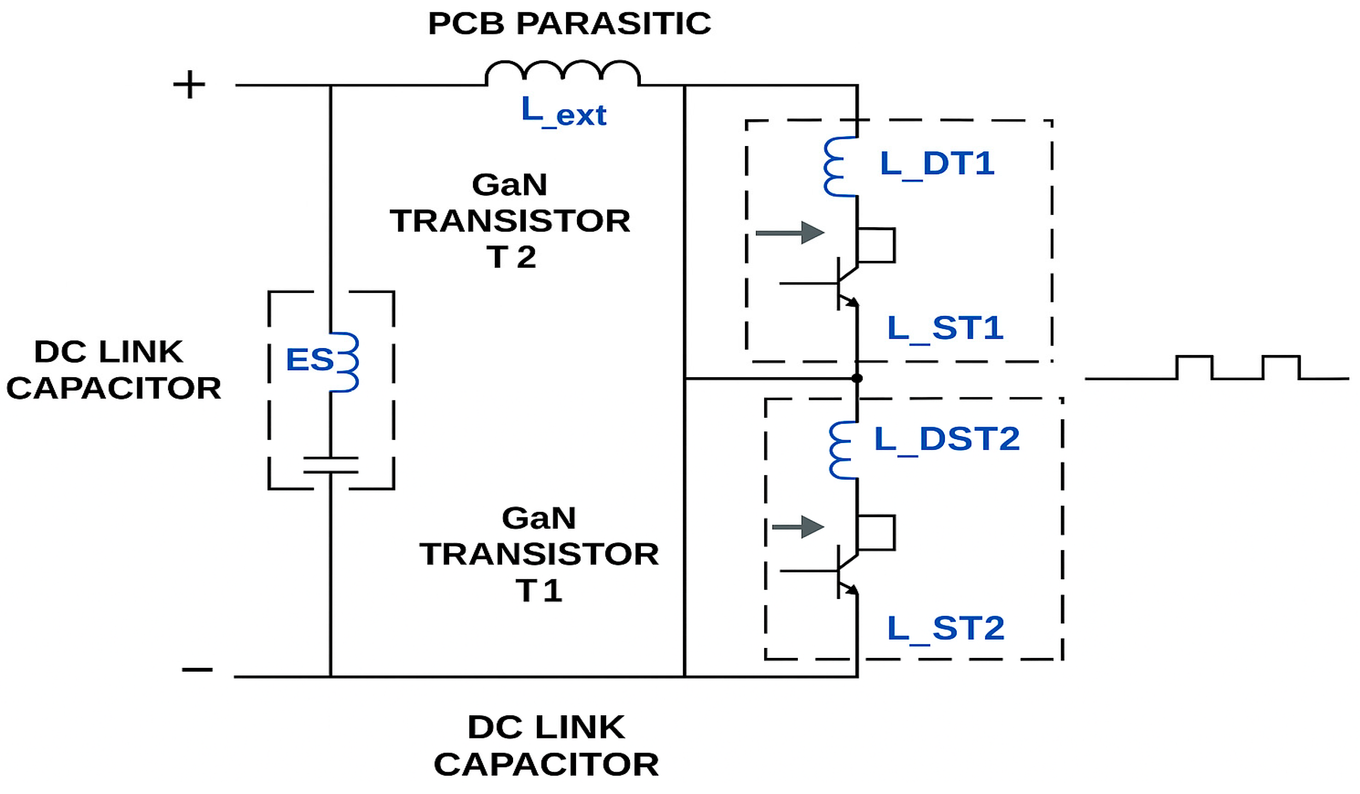
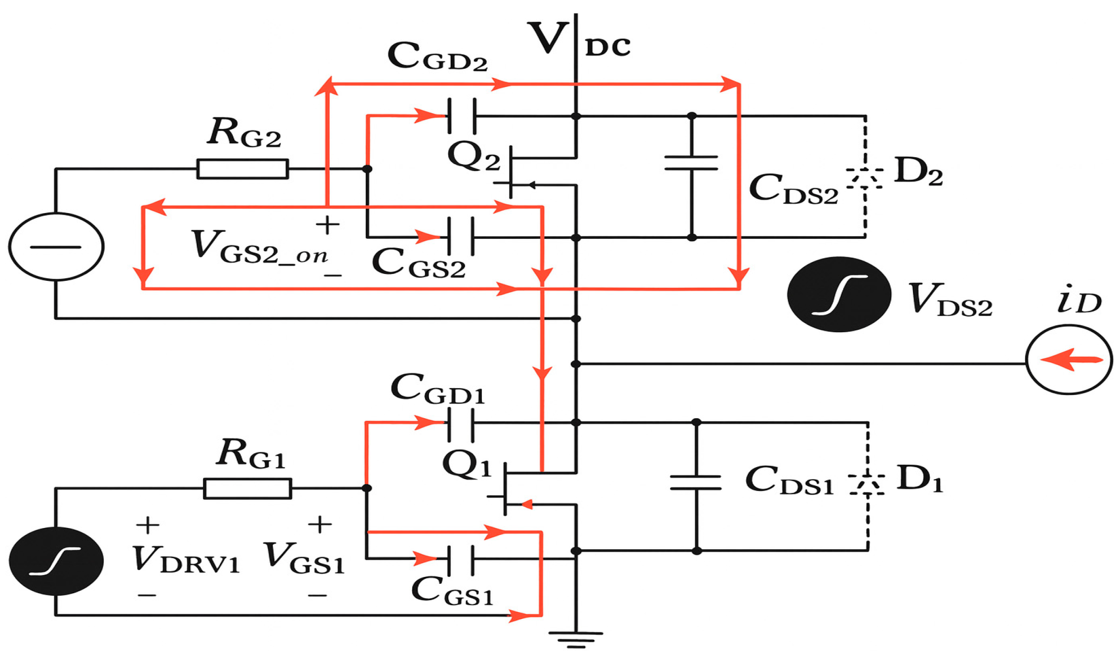
As depicted in Figure 10, the half-bridge parasitic network highlights the external/ESL inductances that create V ( o v e r s h o o t ) ≈ L d i d t and the device/source inductances that shape ringing. As depicted in Figure 11, the gate-loop schematic shows the C g d Miller’s path and the remedies (split R g , active clamp, optional negative bias) used to keep V G S ,   o f f below the threshold during hard edges.
The AC–DC front-end choices in Section 4 determine the operating envelope of the isolated stage that follows. Three-level rectifiers (Vienna, T-type) halve device-node swing and reduce CM injection at the line side, which in turn relaxes the input filter burden and permits a higher switching frequency with an acceptable EMI. The downstream LLC/CLLC or DAB stage should therefore be sized for the front-end’s DC-link ripple, allowable spectrum, and thermal headroom, established in Section 3. In practice, the front-end’s effective ΔV and ripple current set the tank stress, the ZVS margin, and the circulating current of the resonant stage—these dependencies motivate the scaling and ZVS/ZCS trade-offs analyzed in Section 5.

5. DC–DC Stages (LLC/CLLC/DAB): ZVS/ZCS and Scaling Trade-Offs

Isolated DC–DC conversion bridges the AC–DC front end and the battery/DC link. In GaN-based EV chargers, this stage is dominated by resonant LLC/CLLC and dual active bridge (DAB) architectures operating from a few hundred kilohertz up to the low-MHz range to shrink magnetics [69,70]. The design objective is to exploit GaN’s low C o s s and negligible reverse recovery to realize soft switching—primary-side ZVS and, where advantageous, secondary-side ZCS—while preventing circulating current and transformer/core loss from eroding efficiency as frequency scales [71].
For LLC/CLLC, the soft-switching windows follow directly from the tank resonances and quality factor. With the usual definitions, the two relevant resonances for CLLC are [72,73]
f r 1 = 1 2   π   L r   C r ,   f r 2 = 1 2   π   ( L r +   L m )   C r
Equation (19) represents the idealized gain of a lossless tank. In practice, magnetizing current, device output capacitance, and transformer leakage inductance perturb the phase trajectory and shift the ZVS/ZCS boundaries. An accurate design must therefore include these parasitic elements when selecting L r , C r , and the permissible dead time window.
Operating at or above f r 1 typically secures primary-side ZVS, because the tank current during dead time can charge/discharge the switch output capacitances before turn-on; operating near/below f r 2 can promote secondary-side ZCS, reducing rectifier stress [74]. In practice, designers place the nominal switching frequency slightly above f r 1 and regulate around the resonance to balance the ZVS margin against the magnetizing current [75]. Figure 12 shows the LLC/CLLC tanks, indicating f r 1 and f r 2 , and overlays a ZVS/ZCS map versus normalized frequency and load.
The primary ZVS margin can be expressed by an energy balance. Let C e q be the effective capacitance to be commutated (dominated by the device C c o s s ) , V s w the voltage at the switch node, and I d e a d . The tank current during dead time flowing through an effective inductance L e q . ZVS is obtained when [76]
1 2 C e q V s w   2   ( C o s s energy )   1 2 L e q   I d e a d   2 ( inductor   energy   during   dead   time )     I d e a d V s w C e q L e q
Because GaN significantly lowers C e q , the required I d e a d is modest even as f s rises; this is the key enabler for MHz-class LLC/CLLC with compact planar magnetics and manageable circulating power [77]. However, as f s increases, the available dead time shrinks, so   L r ,   L m   , and dead time programming must be co-designed to preserve [69]. These trade-offs are illustrated in Figure 12 by superimposing the constant efficiency contours (from measured P c o r e and R a c     f ) over the ZVS/ZCS regions [78,79].
A second practical axis is the circulating current versus magnetics trade-off. Running above resonance flattens the LLC gain and eases regulation, but it increases the magnetizing current if L m is small; excessive I m a g e   inflates copper loss and hot-spot temperature [80,81]. The transformer design, therefore, co-optimizes the core loss (e.g., Steinmetz P c o r e   =   k f α   B β   V c o r e ) and frequency-dependent copper loss P c u   , using R a c   f models [82]. Overall stage efficiency is tracked by [83]
η = P s w P o u t   +   P s w +   P c o n d   +     P c u   +   P d r v ,
with P s w being largely governed through the ZVS margin, and P c o r e ,     P c u   being increasingly dominant as f s   approaches the low-MHz regime. In GaN hardware, maintaining ZVS with minimal circulating current is the central lever for simultaneously hitting high η and power density.
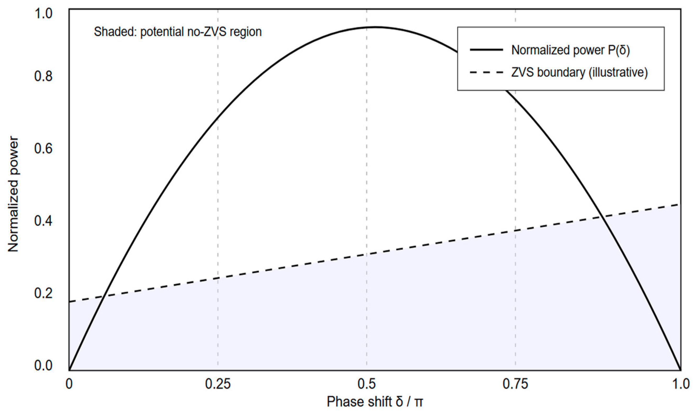
For DAB (single phase-shift, SPS), soft switching is achieved by timing the bridge currents (via the leakage or series inductance L l ) so that device capacitances are commutated before each edge [84]. With square-wave bridges of amplitudes, V 1 and V 2 , the ideal SPS power transfer is [85].
P D A B   ( δ ) = V 1   V 2   ω   L e q         δ ( π δ ) π ,   0   δ   π ,
where δ is the phase shift. For a given L e q   , raising f reduces the required δ at a target power, but off-nominal bus ratios ( V 1     V 2 ) increase RMS current and can jeopardize ZVS at a light load if the inductor current is insufficient during transitions [86]. Designers, therefore, pick the transformer turns ratio to keep δ moderate around the nominal and may add frequency or multi-phase control at the extremes to preserve ZVS [87]. Figure 13 plots P(δ) show typical inductor current waveforms and overlay a ZVS feasibility boundary versus load and ratio V 2 V 1 .
Scaling to 400 V and 800 V platforms follows on from these relations. On 400 V packs, full-bridge LLC/CLLC with 650–700 V GaN is straightforward at f s ≈ 300–800 kHz, with planar magnetics and ZVS margins derived. On 800 V buses [88], designers commonly
I.
Retain 650/700/900 V GaN in three-level bridges (keeping device V d s well below rating).
II.
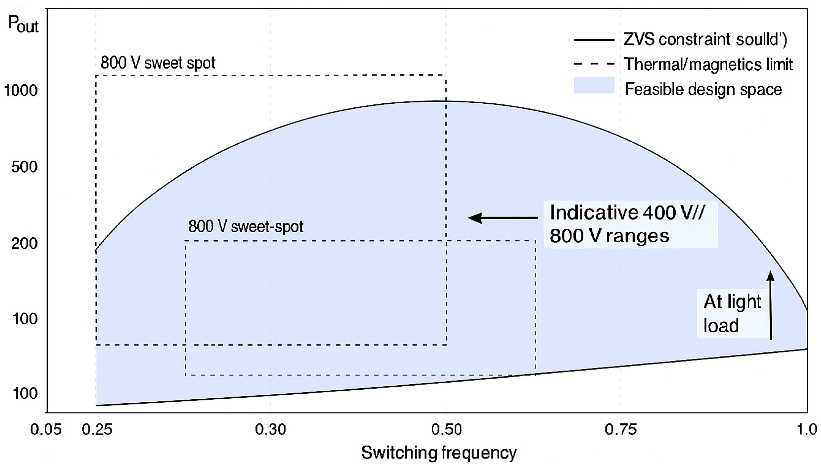
Use DAB with a turns ratio chosen to minimize δ near the nominal, thereby sustaining ZVS across the drive cycle and charging use-cases [89]. The feasible design space over f s and power, constrained by (12) and by transformer flux density limits, is summarized in Figure 14.
Reported implementations align with this picture: multi-CLLC splits the tank currents to reduce device stress at the cost of magnetic complexity; interleaved LLC near 1 MHz attains ZVS with very compact magnetics but demands careful digital timing; DAB at ∼500 kHz achieves bidirectionality and wide-range operation while requiring thermal management of the circulating current when the bus ratio departs from unity [90]. GaN’s soft-switching headroom enables frequency scaling, while the practical limits are the RMS current, magnetic loss, and controller dynamics, all of which feed directly into the system-level efficiency model. As depicted in Figure 12, Figure 13 and Figure 14, the “sweet spot” typically sits where is comfortably met and P c o r e   +   P c u   remain sub-dominant.
Finally, it is useful to connect the DC–DC choices to the EMI strategies (Section 6) and the profile-aware derating maps (Section 3). Higher f s reduces the magnetic size but shifts the switching spectra upward; with GaN’s fast edges, common-mode noise and d v d t couple more strongly into parasites, tank design and gate-loop layout should be co-optimized with the DM/CM filter targets defined in Section 6 [91]. At the same time, the operating point chosen from Figure 12, Figure 13 and Figure 14 must land inside the safe region of the derating maps (Figure 6): raise f s only to the point where thermal headroom and the dynamic R d s   ( o n ) screen remains satisfied with the mission profiles summarized in Figure 5. This cross-link ensures that the resonant/DAB stage does not just meet bench specs but survives real-cycle stresses while passing CISPR-25-conducted EMI requirements [92].
  • Driver tuning and parasitic in resonant DC–DC (LLC/CLLC/DAB).
In resonant stages, the driver’s task is to guarantee ZVS/ZCS with a minimal circulating current. Because the ZVS condition (15) requires sufficient energy in the tank during dead time to commutate device capacitances, the on-edge shaping set by R g ,   o n controls the attainable d v d t and the available I d e a d [93]. A practical design outcome is to choose R g ,   o n so that the ZVS energy balance in (15) is met at a light-to-nominal load, while the switching spectrum remains within the target EMI bands; the off-edge is kept firm with a smaller R g ,   o f f and an active Miller clamp for immunity over the full gain range [94].
The same two parasitic channels define robustness as follows: CSI-induced gate bounce and Miller injection. Using the estimates in (14)–(16) with the resonant stage’s worst-case d i d t and d v d t provides a quantitative immunity screen [95]. Where allowed by the device, a slight negative off-bias can increase the margin to V t h during the high-slew transitions of DAB at off-nominal ratios [96]. Propagation-delay matching and programmed dead time are co-designed with the tank, so ZVS is preserved without excessive third-quadrant conduction; too short invites shoot-through, but too long inflates the circulating current and degrades the loss terms [97]. Isolation and level-shift paths must meet the converter’s CMTI requirement, and bootstrap networks should tolerate the same d v d t [98].
Include driver dissipation in the stage model via [99].
P g d r v = Q G   V D R V   f s   per   device ,
and verify that the chosen edges satisfy ZVS while keeping snubber power (Section 6) acceptable when any residual ringing is damped [100]. For completeness, the off-state immunity and timing constraints can be summarized as
V G S ,       o f f V t h ,       m i n ( V G S ,     b o u n c e   + Δ V G S ,     o f f )
dead   time   t c o m m u t e   ( I d e a d ,   C e q )
C M T L i s o ( d V D d t ) m a x + margin
where V G S ,   b o u n c e     L C S I d i d t (gate bounce from common-source inductance) and Δ V G S ,   o f f is the Miller-induced off-gate rise during fast d v d t .
As depicted in Figure 15a, the recommended gate/power-loop partition uses a Kelvin-source return, highlights the common-source inductance, and keeps the commutation loop compact—this directly relaxes the ZVS current needed in Equation (15). As depicted in Figure 15b, the simplified driver–device view shows the C g d and C g s paths that create the off-gate bump; the split R g and Miller clamp suppresses it and stabilizes the timing at high d v d t .
The preceding analysis of gate-driver coordination and parasitic control completes the discussion of wired resonant converters, where energy transfer is confined to the magnetics and PCB traces.
However, the same physical attributes that make GaN devices attractive in LLC/CLLC and DAB stages—low C o s s , high d v d t capability, and stable ZVS at multi-hundred-kilohertz frequencies—are now transforming contactless and high-specific-power architectures.
These include wireless power-transfer (WPT/CPT) interfaces for conductive-free charging and the electrified propulsion modules used in emerging three-dimensional transportation (eVTOL and omnidirectional vehicles).
These emerging implementations motivate an extended analytical treatment, in which the resonant-converter principles developed above are generalized to spatially coupled and high–high-power-density topologies, yielding equivalent transfer relations and efficiency scaling laws that quantify GaN’s operational limits in wireless and propulsion-grade systems.
  • GaN-Enabled Wireless Transfer and Multidimensional Propulsion Extensions
While the resonant DC–DC analysis above has emphasized hard- and soft-switching coordination within cabled converters, the same GaN switching advantages now extend to contactless power transfer and three-dimensional propulsion platforms.
Both domains reuse the design languages of ZVS/ZCS control, thermal headroom, and EMI constraint described earlier, but operate at higher frequencies and with spatial coupling as the energy-transfer medium.
I.
Wireless Power Transfer (WPT) with Ferrite-Guided Circular Coils
Recent EV charging architectures exploit GaN bridges switching in the 100 kHz–13.56 MHz band to excite loosely coupled coils [101].
A simplified series–series resonant link can be expressed as
η = ω 2   M 2   R L R 1 + R 2 2 + ω 2   M 2     R 1 + R 2 R L  
where M is the mutual inductance, R 1 and R 2 are winding resistances, and R L the reflected load [102].
Because GaN transistors sustain low switching loss at high ω , both M and the coupling coefficient
K = M L 1   L 2
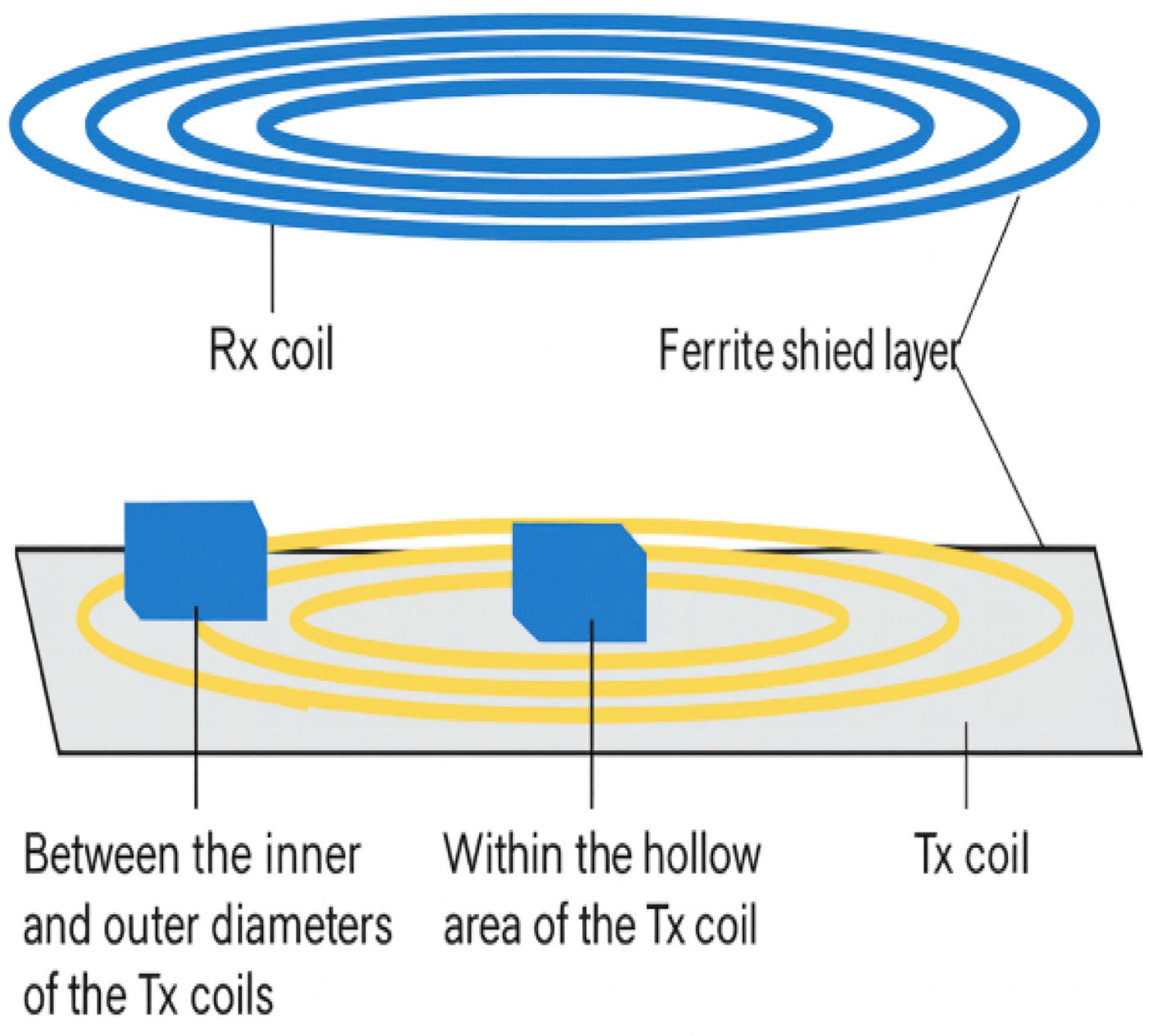
are strongly frequency-dependent [103]. As depicted in Figure 16, the ferrite shield enclosure shapes the magnetic flux and redirects it toward the receiver plane, effectively enhancing vertical coupling while suppressing lateral field leakage and eddy-current loss into the chassis ground plane [104]. This flux guidance increases the local permeability between the coils and mitigates cross-coupling to nearby conductive structures, enabling higher efficiency at moderate air gaps [105].
Designers must, however, re-evaluate the ZVS inequality from (27), using the complex load Z 2 ( ω ,   R L M) to confirm that the available tank energy exceeds the commutation requirement throughout misalignment excursions [106]. The effective detuning factor
ξ = ω ω 0 ω 0
should remain within ±10% to preserve ZVS and maintain soft-switching operation across dynamic alignment states [107]. Excessive detuning enlarges the magnetizing current and may violate EMI constraints by shifting the harmonic envelope toward CISPR-25 limits [108]. Therefore, GaN WPT drivers incorporate adaptive frequency tracking (AFT) and phase-locked resonance control to sustain maximum-efficiency points while minimizing common mode noise [109].
In advanced implementations, ferrite-assisted circular coils are co-simulated with full-bridge GaN drivers in SPICE/Simulink environments to capture the interplay between device switching transients, magnetic coupling variations, and EMI spectral shifts [110]. The high d v d t edges of GaN require coordinated gate-loop shaping and snubber damping to prevent radiated leakage through the ferrite interfaces, a challenge that is increasingly addressed by integrated shield winding or multi-layer ferrite tiles [111].
As shown in Figure 16, the optimized ferrite geometry raises mutual inductance by 20–35% under 30 mm misalignment, while reducing leakage flux density near metallic surfaces by nearly 40% [112]. Such characteristics enable mid-range dynamic charging pads and in-motion (dynamic WPT) systems compatible with GaN-based traction inverters and three-dimensional propulsion concepts [113].
II.
Capacitive Power Transfer (CPT) and Compensation Converter Optimization
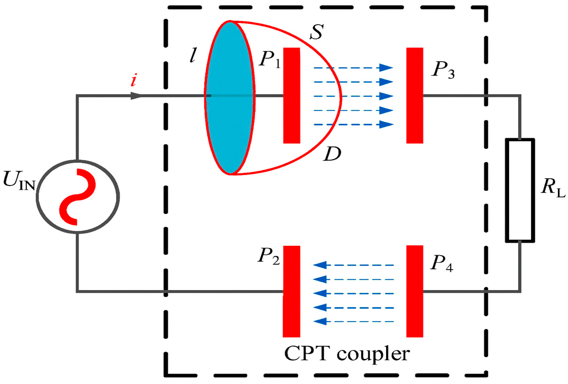
Where magnetic fields are limited—e.g., aluminum chassis or narrow under-body clearance—capacitive power transfer provides galvanic isolation via coupling plates [114].
The total plate reactance, X p = − 1 ω C p , varies with gap and dielectric, so compensation converters are used to achieve a zero-phase angle (ZPA) at the inverter port, minimizing reactive power [115]. For the widely adopted LCL network, ZPA is reached when [116]
ω 2   L s   C e q ( C p ,   C s ,   R L ) 1
ensuring unity power factor (Cos ≈ 1). Alternative LCC and CLC configurations shift part of the reactive cancelation to the secondary side [117,118]:
ω 2 L s C s   1 ,   X p +   X C c   0   X C c =     1 ( ω C C )
These variants enable flexible impedance tuning across different load conditions [119]. The LCC network minimizes the circulating current, offering moderate voltage stress [120], while the CLC configuration achieves the thinnest structural form factor, which is beneficial in confined environments such as vehicle chassis or robotic arms [121].
Comparative analysis shows that LCL compensation provides the broadest ZPA tolerance and the highest coupling stability [122], but at the cost of a larger physical footprint and higher magnetic interaction [123]. LCC compensation optimizes current distribution and voltage-stress balance [124], making it suitable for dynamic load conditions [125]. CLC compensation, on the other hand, achieves a compact geometry with high field uniformity [126], although it exhibits a narrower ZPA bandwidth and greater sensitivity to C P drift or dielectric variation [127].
At higher switching frequencies, GaN-based devices substantially enhance the performance of all three networks [128]. Their ultra-fast switching capability and low output capacitance, C o s s , reduce the phase delay between voltage and current [129], enabling MHz-range CPT operation with minimal loss [130]. The improved edge control and low gate charge allow for precise modulation of the compensation network, resulting in lower reactive circulation and enhanced electromagnetic compatibility [131].
Overall, GaN’s high-speed operation facilitates compact, high-density CPT systems with a reduced component count and superior unity-power-factor (PF) control [132]. It allows for stable ZPA tracking despite capacitive drift, mechanical misalignment, or load fluctuation [133], ensuring reliable power transfer through dielectric-based couplers [134]. The overall configuration and its phasor relationship are illustrated in Figure 17, which depicts the electric-field coupling mechanism and compensation behavior within a representative CPT topology.
The optimization of capacitive power-transfer architectures not only advances high-efficiency charging interfaces but also lays the groundwork for energy routing in dynamic, multi-axis propulsion systems. The same GaN-enabled compensation strategies that sustain zero-phase-angle (ZPA) operation and high power density in stationary CPT modules extend naturally to the domain of three-dimensional electrified transportation, where converters must operate under rapidly varying load, alignment, and thermal conditions. By exploiting MHz-range switching and precise electric-field control, CPT concepts evolve into lightweight, contactless power-distribution frameworks that are capable of feeding distributed drive modules, actuators, and propulsion coils without magnetic bulk or heavy interconnects. These characteristics make GaN-based CPT topologies a key enabler for compact, thermally efficient, and electromagnetically compliant drive platforms used in vertical-take-off, aerial, and omnidirectional vehicles.
Building on these foundations, Section 3 explores how these converter and material advancements transition into full propulsion systems, analyzing GaN-based architectures for high-voltage buses, dual-active-bridge (DAB) and CLLC converters, and multi-phase inverters. The discussion introduces the power-processing factor (PPF) as a unified figure of merit to evaluate converter efficiency, frequency scalability, and electronic mass in next-generation three-dimensional mobility applications.
III.
Electrified Propulsion for Three-Dimensional Transportation
Emerging vertical-take-off and omnidirectional vehicles extend EV electronics into new mechanical dimensions where weight, cooling, and EMI become co-dominant constraints [135].
Each propulsion module typically contains a high-voltage bus, a bidirectional DAB or CLLC converter interfacing the battery, and multi-phase traction inverters.
To evaluate competing topologies, a useful normalized metric is the power-processing factor [77]
PPF = η   f s m e l e c   [ kHz / kg ] ,
which rewards converters that preserve efficiency, η, while raising the switching frequency, f s , and reducing electronic mass, m e l e c [136].
Parameter selection must jointly satisfy three coupled conditions—thermal, soft-switching, and EMI, which are already formalized in previous sections [137]:
T J =   T c o o l ,   i n +   P l o s s ( f s ,   I ,   Δ V )   ( R θ J C +   R θ C a )   T J ,   m a x   H t h ,
1 2   L e q   I d e a d 2 C e q   V S W 2 ,     A D M / C M r e q ( f ) = V m e a ( f ) V l i m ( f ) + M
The intersection of these constraints defines the feasible operating region [138].
GaN’s low R D S ( O N ) and reduced P S W widen this region, achieving higher PPF while maintaining the junction temperature and EMI compliance [46].
As depicted in Figure 18, the design space expands toward a higher frequency and power density compared with Si/SiC counterparts, illustrating the enabling role of GaN in next-generation aerial EV propulsion [139].
This expansion in the GaN design domain translates into measurable propulsion efficiency and weight advantages for aerial electric vehicles (AEVs) and vertical-take-off-and-landing (VTOL) systems [140]. As converter mass and thermal loading scale increase nonlinearly with the switching frequency, GaN’s superior figure of merit (FOM = R D S ( O N ) × Q g ) permits higher f s without excessive conduction or gate-drive losses, thus achieving higher specific power (W/kg) and power density (W/L) ratios than Si- or SiC-based designs [141].
Moreover, by supporting the MHz-class operation, GaN allows for drastic downsizing of the magnetics and capacitive components, which are traditionally dominant in propulsion-stage volume [142]. This improvement directly affects the thrust-to-weight ratio of eVTOL platforms and distributed propulsion arrays, where power converters are co-located with individual motors [143]. The resulting architecture minimizes cabling losses, enhances fault isolation, and simplifies EMI containment across high-voltage bus networks [144].
Thermally, GaN’s reduced switching and conduction losses alleviate the need for bulky heat spreaders and enable integrated liquid-cooling or cold-plate microchannel solutions [145]. These compact thermal paths not only stabilize T j within allowable margins but also maintain soft-switching boundaries over wide ambient and altitude ranges—an essential reliability condition for aerospace-certified propulsion electronics [146].
Furthermore, the enhanced dynamic response and low output capacitance ( C O S S ) of GaN transistors allows for precise modulation of pulse-density or phase-shifted control in CLLC or DAB converters, ensuring continuous soft-switching even under load transients or regenerative braking events [147]. This attribute enhances the bidirectional energy flow and improves the battery-to-thruster efficiency during flight mode transitions [148].
Collectively, these characteristics confirm that GaN is redefining the multi-dimensional performance envelope for electrified propulsion—delivering high efficiency, ultra-fast switching, superior thermal integrity, and compact EMI-compliant power stages that align with the stringent mass–energy balance requirements of next-generation aerial mobility systems.
To extend this performance perspective into long-term operation, it is equally important to evaluate how different converter topologies influence the reliability trajectory of GaN devices under sustained electrical and thermal cycling.
While propulsion-oriented systems demonstrate GaN’s immediate gains in frequency and density, field deployment longevity still hinges on how each topology manages dynamic R D S ( O N ) drift, gate bias stress, and junction temperature gradients over repetitive mission profiles [149].
A comparative reliability view, therefore, complements the preceding functional analysis—linking the architecture-level design choices to device-level endurance.
IV.
Reliability Mapping Across Converter Topologies
While GaN devices offer superior switching performance, their long-term reliability strongly depends on the converter architecture and its associated electrical and thermal stress distribution [150]. Different topologies impose distinct duty profiles on the switches, affecting the junction temperature swing Δ T j , dynamic R D S ( O N ) drift, and gate stress V G S cycling amplitude [151]. Table 2 summarizes the main reliability–topology correlations.
Quantitative mission profile simulations using a 400 V/3.3 kW Vienna rectifier and a 1 MHz GaN-based CLLC converter (adapted from [21,68]) show that the average junction temperature rise is 25–40 °C lower in soft-switching topologies compared to hard-switched buck–boost equivalents at the same output power. This translates to a 2–3× improvement in mean time to failure (MTTF), according to the Arrhenius relationship:
MTTF     e ( E a k   T j   ) ,
where E a is the activation energy for failure, and k is the Boltzmann constant.
Soft-switching topologies, such as CLLC and DAB, therefore, provide a reliability–efficiency co-optimization, whereas TPPFC and buck-derived stages demand stricter gate-driver voltage control and thermal balancing to suppress dynamic R D S ( O N ) degradation.
Overall, mapping reliability against topology reveals that soft-commutated GaN converters (e.g., CLLC, DAB) dominate in sustained operation, due to their low d v d t stress and narrower thermal cycling amplitude, while hard-switched structures (buck, TPPFC) require enhanced gate management and EMI mitigation to achieve comparable device endurance.

6. EMI and Compliance: Dual-LISN DM/CM Workflow and a Practical Topology-Selection Framework

Abbreviations used in this section: electromagnetic interference (EMI), differential-mode (DM), common-mode (CM), and line impedance stabilization network (LISN).
A.
Dual-LISN representation with compact DM/CM emission models
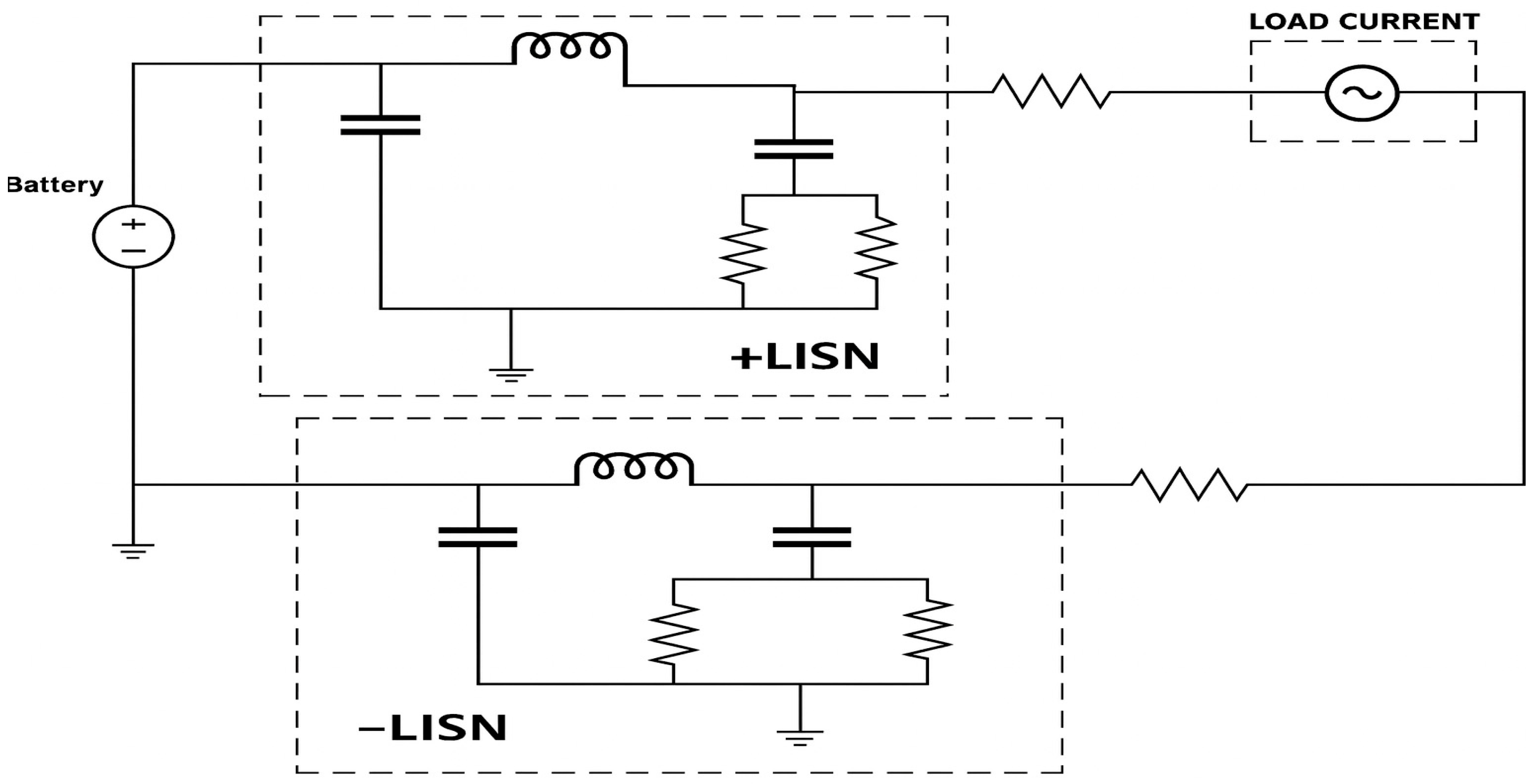
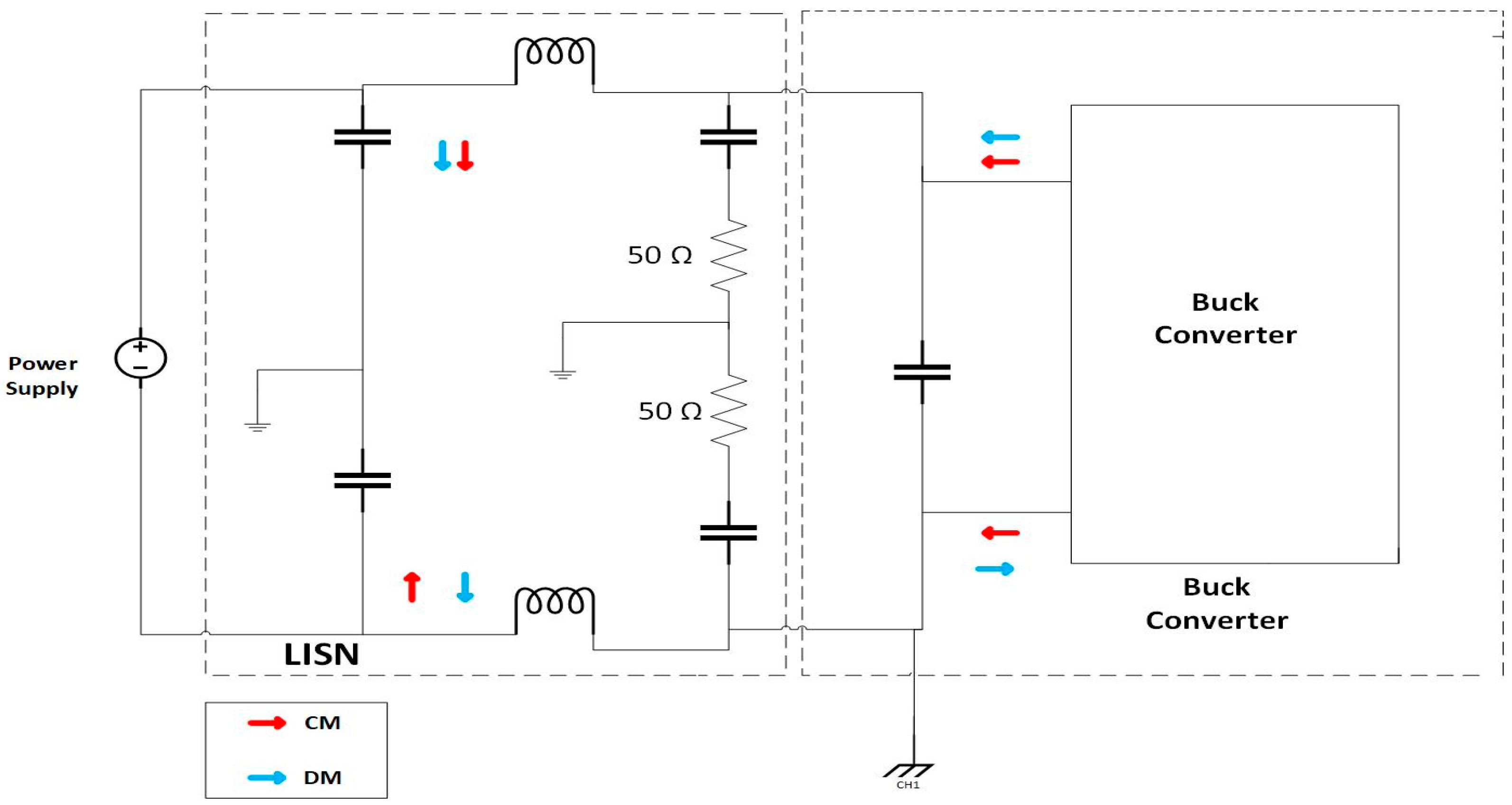
In CISPR-25 style benches for EV power converters, two 5 µH/50 Ω LISNs (line and return) enable the orthogonal reconstruction of differential-mode (DM) and common-mode (CM) conducted emissions from the simultaneously acquired port voltages V + ( f ) and V ( f ) [155]. The standard relations are [156]
V D M ( f ) = V + f V ( f )     2 ,   V C M ( f ) = V + f + V ( f )     2
With each LISN port ~50Ω to ground, the implied noise currents are [157]
I D M = V D M 50   Ω   and   I C M = V C M 50   Ω ( two   shunts   in   parallel )
The analytical relations in (32) assume perfectly balanced LISNs and symmetric cabling. In experimental setups, stray capacitance to chassis and probe loading can distort V D M and V C M . Measurement accuracy improves when the setup is calibrated with a 150 Ω reference source or a verified LISN pair to account for these non-idealities, which also matches the current probe method annotated in Figure 19. Comparing V D M ( f ) and V C M ( f ) (dBµV) to the selected limit lines yields the required attenuation with a modest margin, M, to cover unit-to-unit spread [158]:
A D M r e q ( f ) =   V D M ( f )   V l i m ,       D M ( f ) +   M ,   A C M r e q ( f ) =   V C M ( f )   V l i m ,       C M ( f ) + M
We measured the spectra map naturally to compact physical models. As illustrated in Figure 19, CM noise is driven by the capacitive injection from hot switch nodes, packages, heat-sinks, and interwinding capacitances to the chassis, which was well-approximated by [159]
i C M ( t )     C p a r   d v d t ,
where C p a r is the effective parasite to the chassis. DM content follows the input current slew through the loop inductance in the line/return path [160]:
v p a r ( t )     L p a r   d i d t ,
The high-frequency power that excites the spectrum is bounded by the energy required to commutate device/output capacitances each cycle [161],
E S W   1 2   C O S S V 2 ,   P S W ,       H F   f S   E S W ,
so GaN’s low C o s s is intrinsically favorable—provided the effective dv/dt and high-frequency loop areas are controlled by topology and layout [162]. Figure 20 illustrates these DM/CM return-path mechanisms and the LISN-based reconstruction in (32)–(34).
B.
From attenuation targets to realizable DM/CM networks, with integrated topology/edge-shaping selection and thermal co-constraints
The attenuation targets in (15) define the stopband placement of the DM/CM networks. For a chosen second-order corner and characteristic impedance,
f c = 1 2 π   L C ,   Z O = 1   L C     L = Z O   2 π   f c ,   C = 1 2 π   f c     Z O
first-order element values follow directly. Reported OBC front ends commonly realize DM sections as series-L/shunt-C across the line and return (powder-iron cores tolerate ripple), while CM chokes employ high-µ ferrites with deliberate leakage, so the DM path does not peak [163]. Damping near Z O suppresses residual resonances [164],
  R d a m p   ( 0.3 1 )   Z O   ( placed in series with shunt - C or as an RC across the choke ) ,
and any switch-node snubber is checked against the thermal budget through [165]:
P s n u b   1 2   C s n u b   V 2 f s
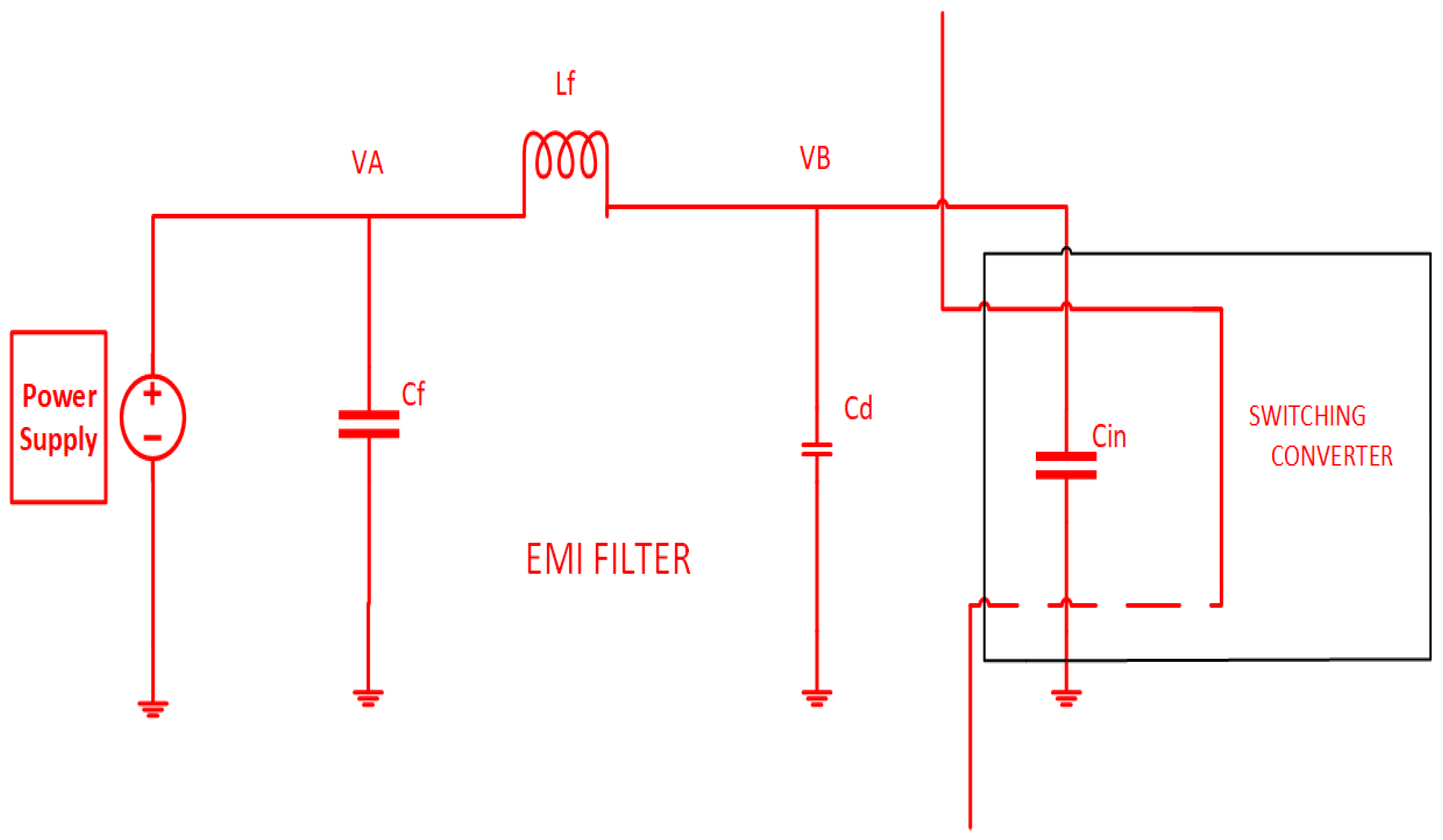
Because the same parasites that generate emissions also determine filter efficacy, layout is a first-stage filter: minimize the switch–capacitor–FET current triangle, provide a Kelvin-source return for the driver, partition “noisy” and “quiet” reference planes with a single CM tie near the LISN side, and maintain creepage from hot nodes to chassis to reduce C p a r and L p a r in (35) and (36) [41]. As depicted in Figure 21, a damped input EMI filter with series L f and shunt C f sets the cutoff; a damping capacitor C d (across C I N ) or an RC branch mitigates peaking between V A and V B .
The DM/CM attenuation targets and any switch-node snubbing consume thermal headroom from the profile-aware derating map in Section 3. Hence, the feasible EMI solution set is the intersection of the following: (i) the ZVS/ZCS conditions and circulating current limits of Section 5, and (ii) the junction-temperature and dynamic- R D S ( O N ) ) screens of Section 3. Designing EMI and reliability concurrently avoids meeting CISPR-25 at the expense of long-term device margins.
C.
Decision map linking EMI, efficiency, power density, and complexity
EMI compliance is co-determined by these networks and by the chosen topology and edge shaping. Soft-switching DC–DC stages (LLC/CLLC/DAB; Section 5) shift energy out of DM-critical bands and lower CM injection by reducing the effective ΔV at switching nodes; three-level AC–DC front ends (Vienna, T-type; Section 4) halve device-node voltage swing relative to two-level legs, easing CM filtering [166].
The feasible operating region is the intersection of:
  • Sufficient ZVS/ZCS margin from the resonant/bridge analysis;
  • The derating map from Section 3 (junction-temperature limit and any dynamic R D S ( O N ) screen);
  • A compact DM/CM network that delivers A r e q   ( f ) from (34) with acceptable damping and P s n u b from (40) [167].
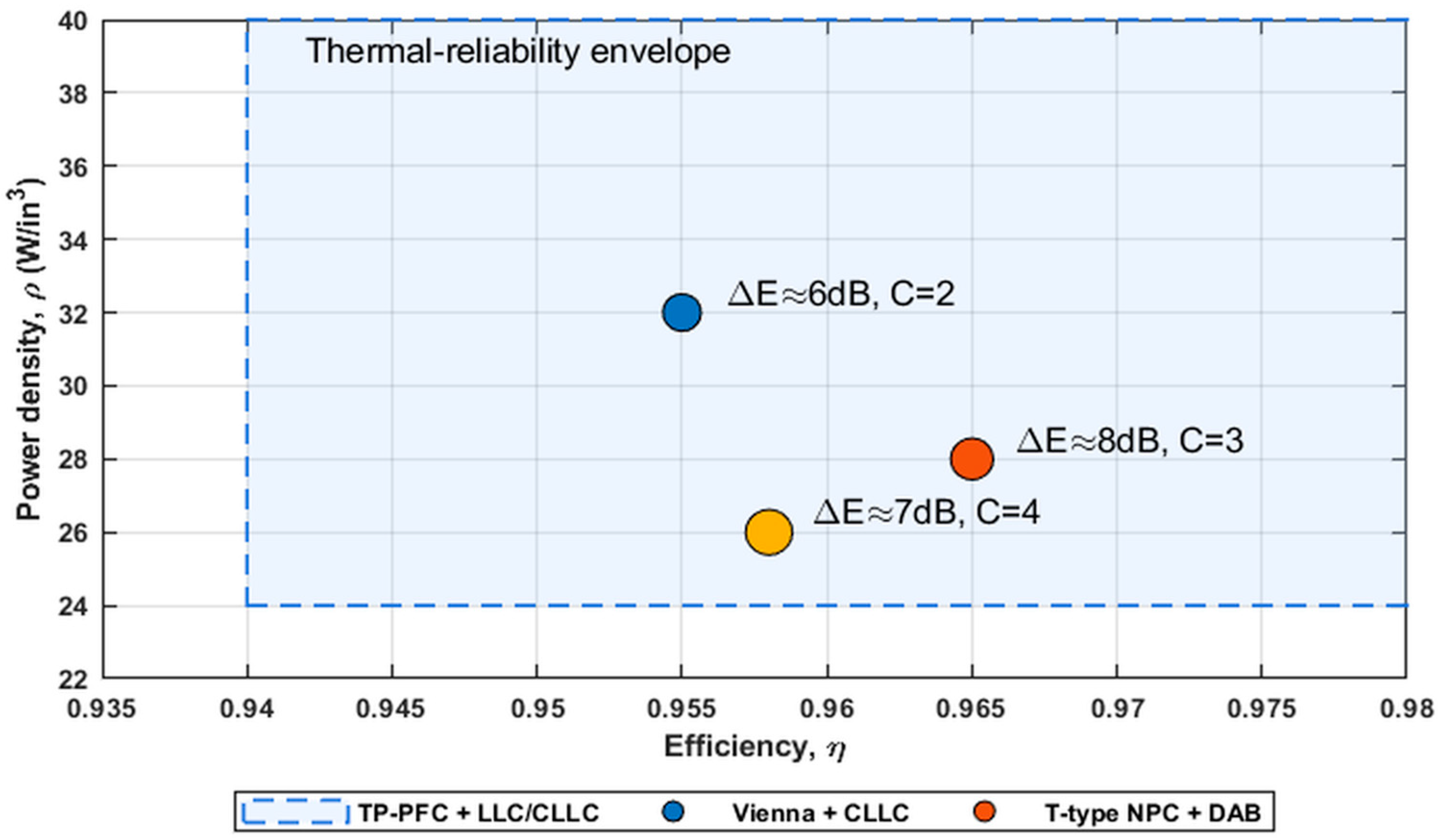
These coupled constraints are conveniently visualized by a Pareto/decision map whose axes are efficiency, η, power density, ρ, EMI margin, ΔE (dB below the limit after filtering), and implementation complexity, C (device/driver count, balancing and control). In such maps, single-phase TP-PFC + LLC/CLLC tends to maximize ρ at moderate C; Vienna + CLLC commonly leads in η and ΔE at a higher power, due to three-level commutation; and T-type NPC + DAB offers native bidirectionality with similar CM advantages but a higher C and circulating current thermal cost [168].
The preferred operating point is where the chosen topology, switching frequency, and d v d t not only meet the attenuation targets, but also lie inside the shaded thermal-reliability region established earlier. As depicted in Figure 22, the Pareto map (η vs. ρ; marker size ∝ complexity; labels give EMI margin ΔE) highlights the feasible operating region as the shaded thermal-reliability envelope and guides the final topology/ f s choice.
The decision map in Figure 22 provides a graphical trade-off among efficiency, power density, EMI margin, and implementation complexity. However, to contextualize this theoretical envelope with experimentally demonstrated systems, it is essential to benchmark the real GaN-based converter results reported in the recent literature. Such comparative evaluation links the analytical framework developed in Section 3, Section 4 and Section 5 with practical data measured under standardized CISPR-25 or DO-160 test environments.
Therefore, a consolidated benchmarking study has been performed, summarizing representative prototypes of GaN-based EV subsystems—including on-board chargers (OBCs), DC–DC converters, and traction inverters—published between 2019 and 2025. Each entry in Table 3 quantifies efficiency (η), volumetric power density (ρ), and EMI margin (ΔE dBµV below the applicable limit), normalized on a per-kilowatt basis to ensure fair comparison across voltage classes and topologies.
This extension transforms the synthesis into a semi-quantitative validation step: it demonstrates how GaN technology simultaneously advances switching frequency, thermal stability, and EMI compliance compared with its Si/SiC counterparts, thereby validating the proposed framework and expanding its relevance beyond analytical modeling to real experimental practice.
The consistency between the Pareto envelope in Figure 16 and the experimental range summarized in Table 3 confirms that GaN technology now occupies the optimal efficiency–density–EMI space for EV power electronics [172]. This alignment validates the proposed decision framework as a predictive design tool for next-generation converter optimization.
While the decision framework in Figure 22 effectively maps efficiency, power density, EMI margin, and implementation complexity, a complete roadmap must also define measurable design milestones. In current EV system development, performance validation requires quantifiable targets rather than qualitative trends. Hence, this section extends the analytical and benchmarking discussion toward a metrics-driven roadmap, establishing explicit technical goals for GaN platforms across 400 V and 800 V domains.
These targets provide the missing link between converter-level optimization and subsystem-level validation, integrating the reliability, thermal, and EMI constraints derived throughout Section 3, Section 4, Section 5 and Section 6. The roadmap serves both as a verification checklist and as a guide for future GaN integration in high-voltage EV architectures. The quantitative metrics, summarized in Table 4, express realistic boundary conditions that next-generation converters must achieve to align with the proposed framework.
Roadmap with Quantitative Targets and Verification Path
To translate the selection framework into deployable specifications, we define the following metrics used throughout the paper:
  • Efficiency: η at rated load (and a light-load point).
  • Power density: ρ in W/L (converter volume excludes cabling).
  • EMI margin: ΔE = (measured DM/CM level − limit) in dBµV, negative is a compliant margin.
  • Power-processing factor: PPF = η   f s M e l e c (Equation (30)).
  • Thermal headroom: H t h = T J ,   m a x T J under mission profile load (Equation (4)).
Table 4 sets platform-specific technical targets for GaN EV subsystems. These values are selected to (i) retain ZVS/ZCS feasibility (Section 5), (ii) remain within the derating envelope (Section 3), and (iii) pass CISPR-25 conducted-EMI with a margin, using the dual-LISN workflow (Section 6).
Achieving the Table 4 milestones while remaining within the thermal reliability and EMI envelope of Figure 16 defines a quantitative benchmark for GaN EV converters. Together with the experimental benchmarking in Table 4, this roadmap transforms the study from a qualitative synthesis into a metrics-validated design framework—linking analytical derivations, empirical data, and verifiable subsystem targets for future 400 V/800 V platforms.

7. Conclusions and Roadmap

This review traced GaN from device physics to EV system design, showing how low charge and high critical fields translate into higher switching frequency, smaller passives, and high efficiency—provided d v d t , parasitics, and thermal paths are co-controlled. Real drive cycle analysis linked device heating and dynamic R D S ( O N ) to vehicle-level thermal budgets; three-level front ends (Vienna, T-type) were shown to halve device stress and ease CM emissions; and isolated stages (LLC/CLLC/DAB) were framed with explicit ZVS/ZCS conditions and scaling limits. A dual-LISN DM/CM workflow tied measured spectra to compact source models and to filter synthesis within thermal headroom, yielding a practical selection map that balances efficiency, power density, EMI margin, and implementation effort.
The proposed roadmap also bridges the gaps identified in the introduction by integrating reliability analysis under real drive cycles, vehicle-level thermal coordination of junction-to-coolant paths with magnetic and EMI losses, and seamless scalability toward 400 V and 800 V EV architectures. By aligning these aspects with measurable EMI and thermal margins, the roadmap transforms open research challenges into actionable design parameters that can be validated through both simulation and hardware prototyping.
Future work should emphasize data-driven parameter extraction—from mission-profile logging to electro-thermal digital twins and lifetime estimation—so that reliability, EMI compliance, and efficiency can be optimized concurrently within a unified design framework.

Funding

This research received no external funding.

Data Availability Statement

No new data were created or analyzed in this study.

Conflicts of Interest

The authors declare no conflict of interest.

References

  1. International Energy Agency (IEA). Global EV Outlook 2024; International Energy Agency (IEA): Paris, France, 2024. [Google Scholar]
  2. Musumeci, S.; Barba, V. Gallium Nitride Power Devices in Power Electronics Applications: State of Art and Perspectives. Energies 2023, 16, 3894. [Google Scholar] [CrossRef]
  3. Erramilli, A.; Roughan, M.; Veitch, D.; Willinger, W. Self-Similar Traffic and Network Dynamics. Proc. IEEE 2002, 90, 800–819. [Google Scholar] [CrossRef]
  4. Udabe, A.; Baraia-Etxaburu, I.; Diez, D.G. Gallium Nitride Power Devices: A State of the Art Review. IEEE Access 2023, 11, 48628–48650. [Google Scholar] [CrossRef]
  5. Chen, K.J.; Häberlen, O.; Lidow, A.; Tsai, C.L.; Ueda, T.; Uemoto, Y.; Wu, Y. GaN-on-Si Power Technology: Devices and Applications. IEEE Trans. Electron. Devices 2017, 64, 779–795. [Google Scholar] [CrossRef]
  6. Reimers, J.; Dorn-Gomba, L.; Mak, C.; Emadi, A. Automotive Traction Inverters: Current Status and Future Trends. IEEE Trans. Veh. Technol. 2019, 68, 3337–3350. [Google Scholar] [CrossRef]
  7. Yilmaz, M.; Krein, P.T. Review of Battery Charger Topologies, Charging Power Levels, and Infrastructure for Plug-In Electric and Hybrid Vehicles. IEEE Trans. Power Electron. 2013, 28, 2151–2169. [Google Scholar] [CrossRef]
  8. Rahman, K.F.; Falina, S.; Mohamed, M.F.P.; Kawarada, H.; Syamsul, M. The Role of Gallium Nitride in the Evolution of Electric Vehicles: Energy Applications, Technology, and Challenges. Appl. Phys. Rev. 2024, 11, 031322. [Google Scholar] [CrossRef]
  9. Soomro, H.A.; Khir, M.H.B.M.; Zulkifli, S.A.B.M.; Abro, G.E.M.; Abualnaeem, M.M. Applications of Wide Bandgap Semiconductors in Electric Traction Drives: Current Trends and Future Perspectives. Results Eng. 2025, 26, 104679. [Google Scholar] [CrossRef]
  10. Dutta, S.; Bauman, J. An Overview of 800 V Passenger Electric Vehicle Onboard Chargers: Challenges, Topologies, and Control. IEEE Access 2024, 12, 105850–105864. [Google Scholar] [CrossRef]
  11. Thermal Management of Electrified Vehicles—A Review. Available online: https://www.mdpi.com/1996-1073/15/4/1326 (accessed on 6 October 2025).
  12. Chakraborty, S.; Hasan, M.M.; Paul, M.; Tran, D.-D.; Geury, T.; Davari, P.; Blaabjerg, F.; Baghdadi, M.E.; Hegazy, O. Real-Life Mission Profile-Oriented Lifetime Estimation of a SiC Interleaved Bidirectional HV DC/DC Converter for Electric Vehicle Drivetrains. IEEE J. Emerg. Sel. Top. Power Electron. 2022, 10, 5142–5167. [Google Scholar] [CrossRef]
  13. Rahman, S.M.I.; Moghassemi, A.; Arsalan, A.; Timilsina, L.; Chamarthi, P.K.; Papari, B.; Ozkan, G.; Edrington, C.S. Emerging Trends and Challenges in Thermal Management of Power Electronic Converters: A State of the Art Review. IEEE Access 2024, 12, 50633–50672. [Google Scholar] [CrossRef]
  14. Abramushkina, E.; Zhaksylyk, A.; Geury, T.; El Baghdadi, M.; Hegazy, O. A Thorough Review of Cooling Concepts and Thermal Management Techniques for Automotive WBG Inverters: Topology, Technology and Integration Level. Energies 2021, 14, 4981. [Google Scholar] [CrossRef]
  15. Moreno, G.; Narumanchi, S.; Feng, X.; Anschel, P.; Myers, S.; Keller, P. Electric-Drive Vehicle Power Electronics Thermal Management: Current Status, Challenges, and Future Directions. J. Electron. Packag. 2022, 144, 011004. [Google Scholar] [CrossRef]
  16. Research Assistant-Bohrium|AI for Science with Global Scientists. Available online: https://www.bohrium.com/paper-details/800-v-electric-vehicle-powertrains-review-and-analysis-of-benefits-challenges-and-future-trends/812529581234847745-3873?utm_source=chatgpt.com (accessed on 6 October 2025).
  17. Friedli, T.; Hartmann, M.; Kolar, J.W. The Essence of Three-Phase PFC Rectifier Systems—Part II. IEEE Trans. Power Electron. 2014, 29, 543–560. [Google Scholar] [CrossRef]
  18. Comparison of Unidirectional Three- and Four-Wire-Based Boost PFC-Rectifier Topologies for Non-Isolated Three-Phase EV On-Board Chargers Under Common-Mode Aspects. Available online: https://www.researchgate.net/publication/356836567_Comparison_of_Unidirectional_Three-_and_Four-Wire-Based_Boost_PFC-Rectifier_Topologies_for_Non-Isolated_Three-Phase_EV_On-Board_Chargers_Under_Common-Mode_Aspects (accessed on 6 October 2025).
  19. Meneghini, M.; De Santi, C.; Abid, I.; Buffolo, M.; Cioni, M.; Khadar, R.A.; Nela, L.; Zagni, N.; Chini, A.; Medjdoub, F.; et al. GaN-Based Power Devices: Physics, Reliability, and Perspectives. J. Appl. Phys. 2021, 130, 181101. [Google Scholar] [CrossRef]
  20. Texas Instruments. Bidirectional CLLLC Resonant Dual Active Bridge (DAB) Reference Design for HEV/EV Onboard Charger; Texas Instruments: Dallas, TX, USA, 2024. [Google Scholar]
  21. Reali, A.; Alemanno, A.; Ronchi, F.; Rossi, C.; Florian, C. Development of GaN-Based, 6.6 kW, 450 V, Bi-Directional On-Board Charger with Integrated 1 kW, 12 V Auxiliary DC-DC Converter with High Power Density. Micromachines 2024, 15, 1470. [Google Scholar] [CrossRef]
  22. Texas Instruments. GaN-Based, 6.6-kW, Bidirectional, Onboard Charger Reference Design; Texas Instruments: Dallas, TX, USA, 2021. [Google Scholar]
  23. Chou, P.-C.; Hsieh, T.-E.; Cheng, S.; Del Alamo, J.A.; Chang, E.Y. Comprehensive Dynamic On-Resistance Assessments in GaN-on-Si MIS-HEMTs for Power Switching Applications. Semicond. Sci. Technol. 2018, 33, 055012. [Google Scholar] [CrossRef]
  24. Wang, W.; Liang, Y.; Zhang, M.; Lin, F.; Wen, F.; Wang, H. Mechanism Analysis of Dynamic On-State Resistance Degradation for a Commercial GaN HEMT Using Double Pulse Test. Electronics 2021, 10, 1202. [Google Scholar] [CrossRef]
  25. Doublet, M.; Defrance, N.; Okada, E.; Pace, L.; Duquesne, T.; Emilien, B.; Yvon, A.; Idir, N.; De Jaeger, J.-C. Investigation of Current Collapse Mechanism on AlGaN/GaN Power Diodes. Electronics 2023, 12, 2007. [Google Scholar] [CrossRef]
  26. Alemanno, A.; Santarelli, A.; Sangiorgi, E.; Florian, C. Characterization of the Dynamic RON of 600 V GaN Switches under Operating Conditions. Electronics 2023, 12, 943. [Google Scholar] [CrossRef]
  27. Barbato, A.; Barbato, M.; Meneghini, M.; Silvestri, M.; Detzel, T.; Haeberlen, O.; Spiazzi, G.; Meneghesso, G.; Zanoni, E. Fast System to Measure the Dynamic On-Resistance of on-Wafer 600 V Normally off GaN HEMTs in Hard-Switching Application Conditions. IET Power Electron. 2020, 13, 2390–2397. [Google Scholar] [CrossRef]
  28. Alemanno, A.; Angelotti, A.M.; Gibiino, G.P.; Santarelli, A.; Sangiorgi, E.; Florian, C. A Reconfigurable Setup for the On-Wafer Characterization of the Dynamic RON of 600 V GaN Switches at Variable Operating Regimes. Electronics 2023, 12, 1063. [Google Scholar] [CrossRef]
  29. Huang, Z.-H.; Tang, S.-W.; Fan, C.-T.; Lin, M.-C.; Wu, T.-L. Dynamic On-Resistance Stability of SiC and GaN Power Devices during High-Frequency (100–300 kHz) Hard Switching and Zero Voltage Switching Operations. Microelectron. Reliab. 2023, 145, 114983. [Google Scholar] [CrossRef]
  30. Thönnessen, A.; Baumgaertner, J.; Fronczek, C.; De Doncker, R.W. Comparison of Switching Losses and Dynamic on Resistance of 600 V-Class GaN HEMTs. In Proceedings of the PCIM Europe 2024; International Exhibition and Conference for Power Electronics, Intelligent Motion, Renewable Energy and Energy Management, Nürnberg, Germany, 11–13 June 2024; VDE Verlag Gmbh: Berlin, Germany, 2024. ISBN 978-3-8007-6262-0. [Google Scholar]
  31. CISPR 25:2021; Vehicles, Boats and Internal Combustion Engines—Radio Disturbance Characteristics—Limits and Methods of Measurement for the Protection of On-Board Receivers. International Electrotechnical Commission: Geneva, Switzerland, 2021.
  32. An Experimental Study on Artificial Intelligence-Based Prediction of Capacitance–Voltage Parameters of Polymer-Interface 6H-SiC/MEH-PPV/Al Schottky Diodes-Güzel-2022-Physica Status Solidi (a)-Wiley Online Library. Available online: https://onlinelibrary.wiley.com/doi/epdf/10.1002/pssa.202100821 (accessed on 6 October 2025).
  33. Temperature-Dependent Dynamic RDS, on Under Different Operating Conditions in Enhancement-Mode GaN HEMTs-Li-2020-IET Power Electronics-Wiley Online Library. Available online: https://ietresearch.onlinelibrary.wiley.com/doi/10.1049/iet-pel.2019.0540 (accessed on 6 October 2025).
  34. del Alamo, J.A.; Joh, J. GaN HEMT Reliability. Microelectron. Reliab. 2009, 49, 1200–1206. [Google Scholar] [CrossRef]
  35. Wang, H.; Blaabjerg, F. Power Electronics Reliability: State of the Art and Outlook. IEEE J. Emerg. Sel. Top. Power Electron. 2021, 9, 6476–6493. [Google Scholar] [CrossRef]
  36. Agirrezabala, E.; Aizpuru, I.; Garrido, D.; Portillo, A. Reliability of Power Semiconductor Modules: A State-of-the-Art Review. IEEE Open J. Power Electron. 2025, 6, 1036–1067. [Google Scholar] [CrossRef]
  37. Shen, J.; Yang, C.; Jing, L.; Li, P.; Wu, H.; Huang, Z.; Hu, S. A Novel Evaluation Methodology for the Reliability and Lifetime of 200 mm E-Mode GaN-on-Si Power HEMTs. IEEE Trans. Power Electron. 2023, 38, 6073–6080. [Google Scholar] [CrossRef]
  38. Lumbreras, D.; Vilella, M.; Zaragoza, J.; Berbel, N.; Jordà, J.; Collado, A. Effect of the Heat Dissipation System on Hard-Switching GaN-Based Power Converters for Energy Conversion. Energies 2021, 14, 6287. [Google Scholar] [CrossRef]
  39. Pace, L.; Idir, N.; Duquesne, T.; De Jaeger, J.-C. Parasitic Loop Inductances Reduction in the PCB Layout in GaN-Based Power Converters Using S-Parameters and EM Simulations. Energies 2021, 14, 1495. [Google Scholar] [CrossRef]
  40. Wang, L.; Li, Z.; Zheng, H. Investigation of Parallel and Orthogonal MIMO Antennas with Two-Notched Structures for Ultra-Wideband Application. Micromachines 2023, 14, 1406. [Google Scholar] [CrossRef]
  41. Tahir, M.; Hu, S.; He, X. Performance Improvement Strategies for Discrete Wide Bandgap Devices: A Systematic Review. Front. Energy Res. 2021, 9, 788689. [Google Scholar] [CrossRef]
  42. Reliability and Qualification|Cirrus Logic. Available online: https://www.cirrus.com/company/quality/product-development/reliability-qualification?utm_source=chatgpt.com (accessed on 6 October 2025).
  43. JESD22-A104: Thermal Cycling Test Standard. Available online: https://eureka.patsnap.com/article/jesd22-a104-thermal-cycling-test-standard?utm_source=chatgpt.com (accessed on 6 October 2025).
  44. CISPR 25/ISO 7637 Automotive LISNs. Available online: https://theemcshop.com/categories/emc-test-equipment/line-impedance-stabilization-networks-lisns/cispr-25-iso-7637-automotive-lisns.html?srsltid=AfmBOorgJnxUUGyMeG4omB70qbWIVvW0S-p_QbNhCLEutYNvQey0oGev&utm_source=chatgpt.com (accessed on 6 October 2025).
  45. Huang, Q.; Huang, A.Q. Review of GaN Totem-Pole Bridgeless PFC. CPSS Trans. Power Electron. Appl. 2017, 2, 187–196. [Google Scholar] [CrossRef]
  46. Bay, O.; Tran, M.T.; El Baghdadi, M.; Chakraborty, S.; Hegazy, O. A Comprehensive Review of GaN-Based Bi-Directional On-Board Charger Topologies and Modulation Methods. Energies 2023, 16, 3433. [Google Scholar] [CrossRef]
  47. Dar, A.R.; Haque, A.; Khan, M.A.; Kurukuru, V.S.B.; Mehfuz, S. On-Board Chargers for Electric Vehicles: A Comprehensive Performance and Efficiency Review. Energies 2024, 17, 4534. [Google Scholar] [CrossRef]
  48. Schweizer, M.; Kolar, J.W. Design and Implementation of a Highly Efficient Three-Level T-Type Converter for Low-Voltage Applications. IEEE Trans. Power Electron. 2013, 28, 899–907. [Google Scholar] [CrossRef]
  49. Prado, E.O.; Bolsi, P.C.; Sartori, H.C.; Pinheiro, J.R. Design of Uninterruptible Power Supply Inverters for Different Modulation Techniques Using Pareto Front for Cost and Efficiency Optimization. Energies 2023, 16, 1314. [Google Scholar] [CrossRef]
  50. Texas Instruments. Comparison of AC/DC Power-Conversion Topologies for Three-Phase Industrial Systems; Texas Instruments: Dallas, TX, USA, 2024. [Google Scholar]
  51. Zhaksylyk, A.; Rasool, H.; Abramushkina, E.; Chakraborty, S.; Geury, T.; El Baghdadi, M.; Hegazy, O. Review of Active Front-End Rectifiers in EV DC Charging Applications. Batteries 2023, 9, 150. [Google Scholar] [CrossRef]
  52. UCC28070A Data Sheet, Product Information and Support|TI.com. Available online: https://www.ti.com/product/UCC28070A?utm_source=chatgpt.com (accessed on 6 October 2025).
  53. Abdel-Rahman, S. Resonant LLC Converter: Operation and Design; Infineon Technologies North America: Durham, NC, USA, 2012. [Google Scholar]
  54. Song, Q.; Zhang, R.; Li, Q.; Zhang, Y. Output Capacitance Loss of GaN HEMTs in Steady-State Switching. IEEE Trans. Power Electron. 2024, 39, 5547–5557. [Google Scholar] [CrossRef]
  55. Liu, J. Optimal-Design-for-High-Frequency-GaN-Based-Totem-Pole-PFC; EEPower: Newton-Le-Willows, UK, 2020. [Google Scholar]
  56. Zhao, H.; Li, Y.; Lin, F.; Yan, Y. Neutral-Point Voltage Balance Control of Three-Level Converter Based on Selection Method of Dynamical Adjustment for Small Voltage Vector. Appl. Sci. 2021, 11, 5076. [Google Scholar] [CrossRef]
  57. Anthon, A.; Zhang, Z.; Andersen, M.A.E.; Franke, T. Efficiency Investigations of a 3 kW T-Type Inverter for Switching Frequencies up to 100 kHz. In Proceedings of the 2014 International Power Electronics Conference (IPEC-Hiroshima 2014-ECCE ASIA), Hiroshima, Japan, 18–21 May 2014; pp. 78–83. [Google Scholar]
  58. Deng, J.; Cheng, H.; Wang, C.; Wu, S.; Si, M. Evaluation and Comprehensive Comparison of H-Bridge-Based Bidirectional Rectifier and Unidirectional Rectifiers. Electronics 2020, 9, 309. [Google Scholar] [CrossRef]
  59. Kolar, J.W.; Drofenik, U.; Minibock, J.; Ertl, H. A New Concept for Minimizing High-Frequency Common-Mode EM1 of Three-Phase PWM Rectifier Systems Keeping High Utilization of the Output Voltage. In Proceedings of the APEC 2000. Fifteenth Annual IEEE Applied Power Electronics Conference and Exposition (Cat. No.00CH37058), New Orleans, LA, USA, 6–10 February 2000. [Google Scholar]
  60. Zhang, H.; Yang, L.; Wang, S.; Puukko, J. Common-Mode EMI Noise Modeling and Reduction with Balance Technique for Three-Level Neutral Point Clamped Topology. IEEE Trans. Ind. Electron. 2017, 64, 7563–7573. [Google Scholar] [CrossRef]
  61. Ramakrishnan, H.; Rangaraju, J. Power Topology Considerations for Electric Vehicle Charging Stations; Document No. SLLA497; 2020. Available online: https://www.ti.com/lit/an/slla497/slla497.pdf?ts=1763301694825 (accessed on 6 October 2025).
  62. Texas Instruments. The Benefits of 650-V GaN FETs for 800-V Power Converters; Texas Instruments: Dallas, TX, USA, 2021. [Google Scholar]
  63. Nouri, S.M.; Alemi-Rostami, M.; Kahe, G. Multi-Objective Optimization of Two-Stage AC–DC Power Supply for Reliability and Efficiency Using NSGA-II and Meta-Heuristic Honey Bee Algorithms. Energy Rep. 2023, 10, 3174–3185. [Google Scholar] [CrossRef]
  64. Vesali, M. A Method to Calculate and Measure Losses and Efficiency in DC-DC Converters. JAREE J. Adv. Res. Electr. Eng. 2023, 7, 52–57. [Google Scholar] [CrossRef]
  65. Lidow, A.; Rooij, M.d.; Strydom, J.; Reusch, D.; Glaser, J. GaN Transistors for Efficient Power Conversion; John Wiley & Sons: Hoboken, NJ, USA, 2019; ISBN 978-1-119-59414-7. [Google Scholar]
  66. EPC. Layout Considerations for GaN-Bodo; EPC: El Segundo, CA, USA, 2021. [Google Scholar]
  67. STMicroelectronics. E-Mode GaN Technology: Tips for Best Driving—Application Note; STMicroelectronics: Singapore, 2021. [Google Scholar]
  68. Mueller, J. Optimizing Gate Driver Layout for LiDAR Applications; Texas Instruments: Dallas, TX, USA, 2020. [Google Scholar]
  69. Ammar, A.M.; Ali, K.; Rogers, D.J. A Bidirectional GaN-Based CLLC Converter for Plug-In Electric Vehicles On-Board Chargers. In Proceedings of the IECON 2020 the 46th Annual Conference of the IEEE Industrial Electronics Society, Singapore, 18–21 October 2020; pp. 1129–1135. [Google Scholar]
  70. Design and Analysis of GaN and Planar Magnetics Based DAB Converter for EV On-Board Chargers. Available online: https://www.researchgate.net/publication/394638899_Design_and_Analysis_of_GaN_and_Planar_Magnetics_based_DAB_Converter_for_EV_On-Board_Chargers?utm_source=chatgpt.com (accessed on 6 October 2025).
  71. Xiao, Y.; Zhang, Z.; Andersen, M.A.E.; Sun, K. Impact on ZVS Operation by Splitting Inductance to Both Sides of Transformer for 1-MHz GaN Based DAB Converter. IEEE Trans. Power Electron. 2020, 35, 11988–12002. [Google Scholar] [CrossRef]
  72. Deng, J.; Li, S.; Hu, S.; Mi, C.C. Ruiqing Ma Design Methodology of LLC Resonant Converters for Electric Vehicle Battery Chargers. IEEE Trans. Veh. Technol. 2014, 63, 1581–1592. [Google Scholar] [CrossRef]
  73. Toshiba Electronic Devices & Storage Corporation. Resonant Circuits and Soft Switching; Toshiba Electronic Devices & Storage Corporation: Kawasaki, Japan, 2019. [Google Scholar]
  74. Scuto, A. Half Bridge Resonant LLC Converters and Primary Side MOSFET Selection; STMicroelectronics: Singapore, 2015. [Google Scholar]
  75. Jung, J.; Kwon, J. Theoretical Analysis and Optimal Design of LLC Resonant Converter. In Proceedings of the 2007 European Conference on Power Electronics and Applications, Aalborg, Denmark, 2–5 September 2007; pp. 1–10. [Google Scholar]
  76. Truong, C.-T.; Choi, S.-J. Improved ZVS Criterion for Series Resonant Converters. IEEE Access 2024, 12, 5333–5344. [Google Scholar] [CrossRef]
  77. Mortazavizadeh, S.A.; Palazzo, S.; Amendola, A.; De Santis, E.; Di Ruzza, D.; Panariello, G.; Sanseverino, A.; Velardi, F.; Busatto, G. High Frequency, High Efficiency, and High Power Density GaN-Based LLC Resonant Converter: State-of-the-Art and Perspectives. Appl. Sci. 2021, 11, 11350. [Google Scholar] [CrossRef]
  78. Jiao, J.; Guo, X.; Wang, C.; You, X.; Li, K. An Improved Time-Domain Analytical Method for LLC Resonant Converters and Dead Time Designs for Zero-Voltage Switching. IET Power Electron. 2023, 16, 1455–1471. [Google Scholar] [CrossRef]
  79. Zhang, B.; Zhao, M.; Huang, P.; Wang, Q. Optimal Design of GaN HEMT Based High Efficiency LLC Converter. Energy Rep. 2022, 8, 1181–1190. [Google Scholar] [CrossRef]
  80. Liu, Y.-C.; Chen, C.; Chen, K.-D.; Syu, Y.-L.; Tsai, M.-C. High-Frequency LLC Resonant Converter with GaN Devices and Integrated Magnetics. Energies 2019, 12, 1781. [Google Scholar] [CrossRef]
  81. Ji, Z.; Min, F.; Dou, Y.; Cao, Z.; Li, X. Optimization of Key Power Loss for LLC Circuits with Planar Transformer in High-Frequency and High-Power Scenarios. AIP Adv. 2021, 11, 055119. [Google Scholar] [CrossRef]
  82. Yamamoto, T.; Bu, Y.; Mizuno, T.; Yamaguchi, Y.; Kano, T. Loss Reduction of Transformer for LLC Resonant Converter Using a Magnetoplated Wire. IEEJ J. Ind. Appl. 2018, 7, 43–48. [Google Scholar] [CrossRef]
  83. Farooq, H.; Khalid, H.A.; Khalid, M.U.; Syed, S.A. Efficiency Analysis of GaN Based LLC Resonant Converter for PV Applications. Eng. Proc. 2022, 20, 31. [Google Scholar]
  84. Shen, K.; Tong, A.; Shao, C.; Hang, L.; He, Y.; Zhang, Y.; Li, G.; Zhang, J. ZVS Control Strategy of Dual Active Bridge DC/DC Converter with Triple-Phase-Shift Modulation Considering RMS Current Optimization-Shen-2019-The Journal of Engineering-Wiley Online Library. J. Eng. 2019, 2019, 4708–4712. Available online: https://ietresearch.onlinelibrary.wiley.com/doi/10.1049/joe.2018.9341?utm_source=chatgpt.com (accessed on 7 October 2025). [CrossRef]
  85. Orsinger, J. DAB Converter Control Using Phase-Shift Modulation; Imperix: Sion, Switzerland, 2022. [Google Scholar]
  86. Kirsten, A.L.; Fraytag, J.; Cúnico, L.M.; de Oliveira, T.H.; Carloto, F.G.; Costa, M.A.D. Series Inductance Design of Dual-Active-Bridge Converter: ZVS Range with Practical Considerations. Int. J. Circuit Theory Appl. 2022, 50, 2423–2438. [Google Scholar] [CrossRef]
  87. Shao, S.; Chen, H.; Wu, X.; Zhang, J.; Sheng, K. Circulating Current and ZVS-on of a Dual Active Bridge DC-DC Converter: A Review. IEEE Access 2019, 7, 50561–50572. [Google Scholar] [CrossRef]
  88. Fei, C.; Gadelrab, R.; Li, Q.; Lee, F.C. High-Frequency Three-Phase Interleaved LLC Resonant Converter with GaN Devices and Integrated Planar Magnetics. IEEE J. Emerg. Sel. Top. Power Electron. 2019, 7, 653–663. [Google Scholar] [CrossRef]
  89. Ponnambalam, R.; Vairavasundaram, I. GaN-Based DC-DC Converters for EV Fast Charging: A Review of Wide Bandgap Devices Technology. Results Eng. 2025, 107548. [Google Scholar] [CrossRef]
  90. Wang, Y.-F.; Chen, B.; Hou, Y.; Meng, Z.; Yang, Y. Analysis and Design of a 1MHz Bi-Directional Multi-CLLC Resonant DC-DC Converter with GaN Devices. IEEE Trans. Ind. Electron. 2019, 67, 1425–1434. [Google Scholar] [CrossRef]
  91. Wu, X.; Gao, X.; Wang, J.; Li, Z.; Du, S.; Gao, S.; Li, F.; Du, J.; Shchurov, N.I.; Zhang, X. Advances in Modeling and Suppression Methods of EMI in Power Electronic Converters of Third-Generation Semiconductor Devices. Electronics 2023, 12, 2348. [Google Scholar] [CrossRef]
  92. Dong, M.; Li, H.; Yin, S.; Wu, Y.; Zhao, Z.; Huamin, J.; See, K.Y. Conducted EMI Estimation on GaN Step-up Resonant Converter for Electric Propulsion System. In Proceedings of the 2022 4th International Conference on Smart Power & Internet Energy Systems (SPIES), Beijing, China, 9–12 December 2022. [Google Scholar]
  93. Sun, B.; Zhang, Z.; Andersen, M.A.E. A Comparison Review of the Resonant Gate Driver in the Silicon MOSFET and the GaN Transistor Application. IEEE Trans. Ind. Appl. 2019, 55, 7776–7786. [Google Scholar] [CrossRef]
  94. Sun, B.; Zhang, Z.; Andersen, M.A.E. Review of Resonant Gate Driver in Power Conversion. In Proceedings of the 2018 International Power Electronics Conference (IPEC-Niigata 2018-ECCE Asia), Niigata, Japan, 20–24 May 2018; pp. 607–613. [Google Scholar]
  95. Liu, X.; Shafie, S.; Radzi, M.A.M.; Azis, N.; Karim, A.H.A. Modelling and Mitigating Oscillation in E-Mode GaN HEMT: A Simulation-Based Approach to Parasitic Inductance Optimization. Microelectron. Reliab. 2024, 152, 115293. [Google Scholar] [CrossRef]
  96. A Gate Driver with a Negative Turn Off Bias Voltage for GaN HEMTs. Available online: https://www.researchgate.net/publication/349934585_A_Gate_Driver_with_a_Negative_Turn_Off_Bias_Voltage_for_GaN_HEMTs?utm_source=chatgpt.com (accessed on 7 October 2025).
  97. Qin, H.; Wang, W.; Peng, Z.; Liu, A.; Bai, S. Characterization and Optimization of Gate Driver Turn-off Voltage for eGaN HEMTs in a Phase-Leg Configuration. Energy Rep. 2022, 8, 908–919. [Google Scholar] [CrossRef]
  98. Lu, Y.; Zhu, J.; Sun, W.; Zhang, Y.; Hu, K.; Yu, Z.; Leng, J.; Cheng, S.; Zhang, S. A 600V High-Side Gate Drive Circuit with Ultra-Low Propagation Delay for Enhancement Mode GaN Devices. In Proceedings of the 2018 IEEE 30th International Symposium on Power Semiconductor Devices and ICs (ISPSD), Chicago, IL, USA, 13–17 May 2018; pp. 80–83. [Google Scholar] [CrossRef]
  99. Semiconductor Components Industries, LLC. AND90004-Analysis of Power Dissipation and Thermal Considerations for High Voltage Gate Drivers; Semiconductor Components Industries, LLC: Scottsdale, AZ, USA, 2020. [Google Scholar]
  100. Fritz, N.; Engelmann, G.; De Doncker, R.W. RC Snubber Design Procedure for Enhanced Oscillation Damping in Wide-Bandgap Switching Cells. In Proceedings of the 2019 21st European Conference on Power Electronics and Applications (EPE ’19 ECCE Europe), Genova, Italy, 3–5 September 2019; pp. 1–10. [Google Scholar]
  101. Liu, M.; Chen, M. Dual-Band Multi-Receiver Wireless Power Transfer: Architecture, Topology, and Control. In Proceedings of the 2019 IEEE Applied Power Electronics Conference and Exposition (APEC), Anaheim, CA, USA, 17–21 March 2019; pp. 851–859. [Google Scholar]
  102. Henriques, E.d.M.; Stegen, S. Concave Ferrite Core for Wireless Power Transfer (WPT). Energies 2023, 16, 4553. [Google Scholar] [CrossRef]
  103. Yadav, A.; Bera, T.K. Ferrite Shielding Thickness and Its Effect on Electromagnetic Parameters in Wireless Power Transfer for Electric Vehicles (EVs). J. Eng. Appl. Sci. 2023, 70, 132. [Google Scholar] [CrossRef]
  104. Ito, Y.; Imura, T.; Hori, Y. Leakage Magnetic Field Suppression Method Using the Next Transmission Coil as a Cancel Coil with Ferrite and Shield in Dynamic Wireless Power Transfer. In Proceedings of the 6th International Electric Vehicle Technology Conference, Yokohama, Japan, 22–24 May 2023. [Google Scholar]
  105. Eaker, M.; Berger, D. Understanding CISPR25 Current Probe and Voltage Method for Conducted Emissions; Texas Instruments: Dallas, TX, USA, 2022. [Google Scholar]
  106. Rhee, J.; Woo, S.; Lee, C.; Ahn, S. Selection of Ferrite Depending on Permeability and Weight to Enhance Power Transfer Efficiency in Low-Power Wireless Power Transfer Systems. Energies 2024, 17, 3816. [Google Scholar] [CrossRef]
  107. Design and Analysis of Magnetic Shielding Mechanism for Wireless Power Transfer System Based on Composite Materials. Available online: https://www.mdpi.com/2079-9292/11/14/2187?utm_source=chatgpt.com (accessed on 22 October 2025).
  108. Wu, C.; Kim, H.; Penugonda, S.; Fan, J. Analysis and Modeling of the Common-Mode Conducted EMI From a Wireless Power Transfer System for Mobile Applications. IEEE Trans. Electromagn. Compat. 2021, 63, 2143–2150. [Google Scholar] [CrossRef]
  109. Variable-Frequency Pulse Width Modulation Circuits for Resonant Wireless Power Transfer. Available online: https://www.mdpi.com/1996-1073/14/12/3656?utm_source=chatgpt.com (accessed on 22 October 2025).
  110. Reactive Shield for Reducing the Magnetic Field of a Wireless Power Transfer System with Dipole Coil Structure. Available online: https://www.mdpi.com/2079-9292/13/9/1712?utm_source=chatgpt.com (accessed on 22 October 2025).
  111. Yadav, A.; Bera, T.K. Design and Optimization of Circular and Rectangular Couplers for Wireless Power Transfer: Efficiency Enhancement and Human Safety Assessment. Discov. Energy 2025, 5, 7. [Google Scholar] [CrossRef]
  112. Jaafari, S.; El Hafdaoui, H.; Ajabboune, K.; Khallaayoun, A.; Ahouzi, E. Optimization of Circular Coils with Ferrite Boxes for Enhanced Efficiency in Wireless Power Transfer for Electric Vehicles. Green Energy Intell. Transp. 2025, 4, 100195. [Google Scholar] [CrossRef]
  113. Zhu, L.; Liu, Z.; Ma, L.; Zeng, X.; Lu, W. Analytical and Experimental Investigations of Magnetic Field Distribution for Wireless Power Transfer System with Ferrite Core. Space Sol. Power Wirel. Transm. 2025, 2, 110–115. [Google Scholar] [CrossRef]
  114. Lecluyse, C.; Minnaert, B.; Kleemann, M. A Review of the Current State of Technology of Capacitive Wireless Power Transfer. Energies 2021, 14, 5862. [Google Scholar] [CrossRef]
  115. Lu, J.; Zhu, G.; Lin, D.; Zhang, Y.; Jiang, J.; Mi, C.C. Unified Load-Independent ZPA Analysis and Design in CC and CV Modes of Higher Order Resonant Circuits for WPT Systems. IEEE Trans. Transp. Electrif. 2019, 5, 977–987. [Google Scholar] [CrossRef]
  116. Zhang, H.; Lu, F.; Hofmann, H.; Liu, W.; Mi, C.C. A Four-Plate Compact Capacitive Coupler Design and LCL-Compensated Topology for Capacitive Power Transfer in Electric Vehicle Charging Application. IEEE Trans. Power Electron. 2016, 31, 8541–8551. [Google Scholar] [CrossRef]
  117. Lu, J.; Zhu, G.; Lin, D.; Zhang, Y.; Wang, H.; Mi, C.C. Realizing Constant Current and Constant Voltage Outputs and Input Zero Phase Angle of Wireless Power Transfer Systems with Minimum Component Counts. IEEE Trans. Intell. Transp. Syst. 2021, 22, 600–610. [Google Scholar] [CrossRef]
  118. Wang, Y.; Zhang, H.; Lu, F. Review, Analysis, and Design of Four Basic CPT Topologies and the Application of High-Order Compensation Networks. IEEE Trans. Power Electron. 2022, 37. [Google Scholar] [CrossRef]
  119. A Review of Capacitive Power Transfer Technology for Electric Vehicle Applications. Available online: https://www.mdpi.com/2079-9292/12/16/3534?utm_source=chatgpt.com (accessed on 22 October 2025).
  120. Liu, X.; Clare, L.; Yuan, X.; Wang, C.; Liu, J. A Design Method for Making an LCC Compensation Two-Coil Wireless Power Transfer System More Energy Efficient Than an SS Counterpart. Energies 2017, 10, 1346. [Google Scholar] [CrossRef]
  121. Luo, B.; Mai, R.; Guo, L.; Wu, D.; He, Z. LC–CLC Compensation Topology for Capacitive Power Transfer System to Improve Misalignment Performance. IET Power Electron. 2019, 12, 2626–2633. [Google Scholar] [CrossRef]
  122. Chen, T.; Cheng, C.; Zhang, X.; Li, G.; Guo, Y.; Mi, C.C. A Double-Sided LCL-Compensated Network for the Strongly Coupled CPT System with Minimum Plate Voltage Stresses. IEEE J. Emerg. Sel. Top. Power Electron. 2024, 12, 4275–4287. [Google Scholar] [CrossRef]
  123. Namiki, H.; Imura, T.; Hori, Y. Comparison of Multiple Circuits Including LCL in Inductive Power Transfer and Capacitive Power Transfer. In Proceedings of the IECON 2023-49th Annual Conference of the IEEE Industrial Electronics Society, Singapore, 16–19 October 2023; pp. 1–7. [Google Scholar]
  124. Cheng, C.; Lu, F.; Zhou, Z.; Li, W.; Deng, Z.; Li, F.; Mi, C. A Load-Independent LCC-Compensated Wireless Power Transfer System for Multiple Loads with a Compact Coupler Design. IEEE Trans. Ind. Electron. 2020, 67, 4507–4515. [Google Scholar] [CrossRef]
  125. ElGhanam, E.; Hassan, M.; Osman, A. Design of a High Power, LCC-Compensated, Dynamic, Wireless Electric Vehicle Charging System with Improved Misalignment Tolerance. Energies 2021, 14, 885. [Google Scholar] [CrossRef]
  126. Lian, J.; Qu, X.; Chen, X.; Mi, C.C. Design of a Double-Sided LCLC -Compensated Capacitive Power Transfer System with Predesigned Coupler Plate Voltage Stresses. IEEE J. Emerg. Sel. Top. Power Electron. 2022, 10, 128–137. [Google Scholar] [CrossRef]
  127. Lu, F.; Zhang, H.; Mi, C. A Review on the Recent Development of Capacitive Wireless Power Transfer Technology. Energies 2017, 10, 1752. [Google Scholar] [CrossRef]
  128. Muharam, A.; Mostafa, T.M.; Ahmad, S.; Masuda, M.; Obara, D.; Hattori, R.; Hapid, A. Preliminary Study of 50 W Class-E GaN FET Amplifier for 6.78 MHz Capacitive Wireless Power Transfer. J. Mechatron. Electr. Power Veh. Technol. 2020, 11, 22–29. [Google Scholar] [CrossRef]
  129. Kasper, M. Analysis of Capacitive Power Transfer GaN ISOP Multi-Cell DC/DC Converter Systems for Single-Phase Telecom Power Supply Modules. In Proceedings of the IECON 2016-42nd Annual Conference of the IEEE Industrial Electronics Society, Florence, Italy, 23–26 October 2016. [Google Scholar] [CrossRef]
  130. Amir, M.; Saifi, I.A.; Waseem, M.; Tariq, M. A Critical Review of Compensation Converters for Capacitive Power Transfer in Wireless Electric Vehicle Charging Circuit Topologies. Green Energy Intell. Transp. 2025, 4, 100196. [Google Scholar] [CrossRef]
  131. Iero, D.; Carotenuto, R.; Merenda, M.; Pezzimenti, F.; Della Corte, F.G. Performance Evaluation of Silicon and GaN Switches for a Small Wireless Power Transfer System. Energies 2022, 15, 3029. [Google Scholar] [CrossRef]
  132. A Very-High-Power-Transfer-Density GaN-Based Capacitive Wireless Power Transfer System. Available online: https://www.researchgate.net/publication/321788602_A_very-high-power-transfer-density_GaN-based_capacitive_wireless_power_transfer_system?utm_source=chatgpt.com (accessed on 22 October 2025).
  133. Wang, Z.; Zhang, Y.; He, X.; Luo, B.; Mai, R. Research and Application of Capacitive Power Transfer System: A Review. Electronics 2022, 11, 1158. [Google Scholar] [CrossRef]
  134. Lecluyse, C.; Minnaert, B.; Ravyts, S.; Kleemann, M. Influence of a Medium on Capacitive Power Transfer Capability. In Proceedings of the 2022 Wireless Power Week (WPW), Bordeaux, France, 5–8 July 2022; pp. 589–594. [Google Scholar]
  135. Li, W.; Liu, J.; Gong, C. High-Frequency Response Current Direct Demodulation Method for Sensorless Control of Interior Permanent Magnet Synchronous Motor Drives. J. Power Electron. 2022, 22, 784–795. [Google Scholar] [CrossRef]
  136. He, H.; Lu, Z.; Zhang, C.; Wang, Y.; Guo, W.; Zhao, S. A Data-Driven Method for Dynamic Load Forecasting of Scraper Conveyer Based on Rough Set and Multilayered Self-Normalizing Gated Recurrent Network. Energy Rep. 2021, 7, 1352–1362. [Google Scholar] [CrossRef]
  137. Luo, L.; Qu, Y.; Gong, W.; Qin, L.; Li, W.; Sun, Y. Effect of Particle Size on the Aerobic and Anaerobic Digestion Characteristics of Whole Rice Straw. Energies 2021, 14, 3960. [Google Scholar] [CrossRef]
  138. Sun, R.; Lai, J.; Chen, W.; Zhang, B. GaN Power Integration for High Frequency and High Efficiency Power Applications: A Review. IEEE Access 2020, 8, 15529–15542. [Google Scholar] [CrossRef]
  139. Shivani; Kaur, D.; Ghosh, A.; Kumar, M. A Strategic Review on Gallium Oxide Based Power Electronics: Recent Progress and Future Prospects. Mater. Today Commun. 2022, 33, 104244. [Google Scholar] [CrossRef]
  140. Shermukhamedov, S.; Probst, M. Sputtering from Rough Tungsten Surfaces: Data-Driven Molecular Dynamics Simulations. Phys. Plasmas 2023, 12, 123901. Available online: https://pubs.aip.org/aip/pop/article/30/12/123901/2925622/Sputtering-from-rough-tungsten-surfaces-Data (accessed on 22 October 2025). [CrossRef]
  141. He, P.; Mallik, A.; Sankar, A.; Khaligh, A. Design of a 1-MHz High-Efficiency High-Power-Density Bidirectional GaN-Based CLLC Converter for Electric Vehicles. IEEE Trans. Veh. Technol. 2019, 68, 213–223. [Google Scholar] [CrossRef]
  142. Embarking on a New Frontier of Power Density with GaN|Electronic Design. Available online: https://www.electronicdesign.com/technologies/power/article/55241919/electronic-design-embarking-on-a-new-frontier-of-power-density-with-gan?utm_source=chatgpt.com (accessed on 22 October 2025).
  143. Wei, Y.; Maksudul Hossain, M.; Alan Mantooth, H. GaN HEMT and Air Core Magnetics Based Power Converters Evaluations at Cryogenic Temperature. IOP Conf. Ser. Mater. Sci. Eng. 2024, 1302, 012026. [Google Scholar] [CrossRef]
  144. High-Density Power-Conversion Technology Enablers Using GaN-Power Electronic Tips. Available online: https://www.powerelectronictips.com/high-density-power-conversion-technology-enablers-using-gan/?utm_source=chatgpt.com (accessed on 22 October 2025).
  145. Assessing Reliability and Lifetime of GaN Power Devices-Power Electronics News. Available online: https://www.powerelectronicsnews.com/assessing-reliability-and-lifetime-of-gan-power-devices/?utm_source=chatgpt.com (accessed on 22 October 2025).
  146. Ma, C.-T.; Gu, Z.-H. Review of GaN HEMT Applications in Power Converters over 500 W. Electronics 2019, 8, 1401. [Google Scholar] [CrossRef]
  147. Talukder, A.; Ifty, M.R.; Al Fahad, A. Comprehensive Review of GaN HEMTs: Architectures, Recent Developments, Reliability Concerns, Challenges, and Multifaceted Applications. E-Prime-Adv. Electr. Eng. Electron. Energy 2025, 13, 101059. [Google Scholar] [CrossRef]
  148. Cook, T.; Franconi, N.; Shea, B.; Wilson, C.; Grainger, B.M.; George, A.D.; Barchowsky, A. Radiation-Tolerant, GaN-Based Point of Load Converters for Small Spacecraft Missions. In Proceedings of the 32nd Annual AIAA/USU Conference on Small Satellites, Logan, UT, USA, 4–9 August 2018. [Google Scholar]
  149. Mondy, T. Reliability Study of Enhancement Mode Gallium Nitride Field Effect Transistors; NASA: Washington, DC, USA, 2022. [Google Scholar]
  150. Islam, N.; Mohamed, M.F.P.; Khan, M.F.A.J.; Falina, S.; Kawarada, H.; Syamsul, M. Reliability, Applications and Challenges of GaN HEMT Technology for Modern Power Devices: A Review. Crystals 2022, 12, 1581. Available online: https://www.mdpi.com/2073-4352/12/11/1581?utm_source=chatgpt.com (accessed on 23 October 2025). [CrossRef]
  151. Cusumano, P.; Sirchia, A.; Vella, F. Evaluation of Dynamic On-Resistance and Trapping Effects in GaN on Si HEMTs Using Rectangular Gate Voltage Pulses. Electronics 2025, 14, 2791. [Google Scholar] [CrossRef]
  152. Niu, P.; Guo, J.; Gao, Z.; Yan, J.; Gao, S. Research on Improved Technology of Totem-Pole Bridgeless PFC Circuit Based on Triangular Current Mode. Energies 2025, 18, 3886. Available online: https://www.mdpi.com/1996-1073/18/14/3886?utm_source=chatgpt.com (accessed on 23 October 2025). [CrossRef]
  153. Zhou, K.; Wu, Y.; Wu, X.; Sun, Y.; Teng, D.; Liu, Y. Research and Development Review of Power Converter Topologies and Control Technology for Electric Vehicle Fast-Charging Systems. Electronics 2023, 12, 1581. [Google Scholar] [CrossRef]
  154. Xu, S.; Xu, S.; Xu, D.; Qian, Q.; Sun, W.; Zhu, J. A Review on Recent Effort of Conductive EMI Suppression Methods in High-Frequency Power Converters. IET Power Electron. 2022, 15, 1921–1935. Available online: https://digital-library.theiet.org/doi/full/10.1049/pel2.12348?utm_source=chatgpt.com (accessed on 23 October 2025). [CrossRef]
  155. Krismer, F.; Schroth, S.; Ertl, H.; Kostov, K.S.; Nee, H.-P.; Kolar, J.W. Analysis and Practical Relevance of CM/DM EMI Noise Separator Characteristics. IEEE Trans. Power Electron. 2017, 32, 3112–3127. [Google Scholar] [CrossRef]
  156. Rebholz, H.; Tenbohlen, S. Prospects and Limits of Common- and Differential-Mode Separation for the Filter Development Process. In Proceedings of the 2008 International Symposium on Electromagnetic Compatibility-EMC Europe, Hamburg, Germany, 8–12 September 2008; pp. 1–6. [Google Scholar]
  157. Wang, S.; Lee, F.C.; Odendaal, W.G. Characterization, Evaluation, and Design of Noise Separator for Conducted EMI Noise Diagnosis. IEEE Trans. Power Electron. 2005, 20, 974–982. [Google Scholar] [CrossRef]
  158. Nussbaumer, T.; Heldwein, M.L.; Kolar, J.W. Differential Mode Input Filter Design for a Three-Phase Buck-Type PWM Rectifier Based on Modeling of the EMC Test Receiver. IEEE Trans. Ind. Electron. 2006, 53, 1649–1661. [Google Scholar] [CrossRef]
  159. Kotny, J.-L.; Margueron, X.; Idir, N. High-Frequency Model of the Coupled Inductors Used in EMI Filters. IEEE Trans. Power Electron. 2012, 27, 2805–2812. [Google Scholar] [CrossRef]
  160. Wang, Q.; An, Z.; Zheng, Y.; Yang, Y. Parameter Extraction of Conducted Electromagnetic Interference Prediction Model and Optimisation Design for a DC–DC Converter System. IET Power Electron. 2013, 6, 1449–1461. [Google Scholar] [CrossRef]
  161. Kasper, M.; Burkart, R.M.; Deboy, G.; Kolar, J.W. ZVS of Power MOSFETs Revisited. IEEE Trans. Power Electron. 2016, 31, 8063–8067. [Google Scholar] [CrossRef]
  162. Zhang, B.; Wang, S. A Survey of EMI Research in Power Electronics Systems with Wide-Bandgap Semiconductor Devices. IEEE J. Emerg. Sel. Top. Power Electron. 2020, 8, 626–643. [Google Scholar] [CrossRef]
  163. Lai, R.; Maillet, Y.; Wang, F.; Wang, S.; Burgos, R.; Boroyevich, D. An Integrated EMI Choke for Differential-Mode and Common-Mode Noise Suppression. IEEE Trans. Power Electron. 2010, 25, 539–544. [Google Scholar] [CrossRef]
  164. Erickson, R.W. Optimal Single Resistors Damping of Input Filters. In Proceedings of the APEC ’99. Fourteenth Annual Applied Power Electronics Conference and Exposition, 1999 Conference Proceedings (Cat. No.99CH36285), Dallas, TX, USA, 14–18 March 1999; Volume 2, pp. 1073–1079. [Google Scholar]
  165. Todd, C. Snubber Circuits: Theory, Design and Application; Texas Instruments: Dallas, TX, USA, 1993. [Google Scholar]
  166. Gulur, S.; Iyer, V.M.; Bhattacharya, S. Improved Common Mode Noise Models for Three Level T-Type Neutral Point Clamped Converters. In Proceedings of the 2018 IEEE Energy Conversion Congress and Exposition (ECCE), Portland, OR, USA, 23–27 September 2018; pp. 6398–6403. [Google Scholar]
  167. Kolar, J.W.; Biela, J.; Minibock, J. Exploring the Pareto Front of Multi-Objective Single-Phase PFC Rectifier Design Optimization-99.2% Efficiency vs. 7 kW/Dm3 Power Density. In Proceedings of the 2009 IEEE 6th International Power Electronics and Motion Control Conference, Wuhan, China, 17–20 May 2009. [Google Scholar]
  168. Oh, H.-S.; Hong, S.-Y.; Lee, J.; Lee, J.-B. Comparison of Bi-Directional Topologies for On-Board Charger: A 10.9 kW High-Efficiency High Power Density of DC-DC Stage. Energies 2024, 17, 5496. [Google Scholar] [CrossRef]
  169. Kundu, A.; Patrick, E.; Currlin, S.; Madler, R.; Delgado, F.; Fahmy, A.; Verplancke, R.; Ballini, M.; Braeken, D.; de Beeck, M.O.; et al. Using Compound Neural Action Potentials for Functional Validation of a High-Density Intraneural Interface: A Preliminary Study. Micromachines 2024, 15, 280. [Google Scholar] [CrossRef] [PubMed]
  170. Cacciato, M.; Aiello, G.; Gennaro, F.; Mita, S.; Patti, D.; Scelba, G.; Sujeeth, A. Power Loss Modelling of GaN HEMT Based 3L ANPC Three Phase Inverter for Different PWM Techniques. arXiv 2022. [Google Scholar] [CrossRef]
  171. Varga, D. Analysis of Benford’s Law for No-Reference Quality Assessment of Natural, Screen-Content, and Synthetic Images. Electronics 2021, 10, 2378. [Google Scholar] [CrossRef]
  172. Martin, D.; Curbow, A. High Power Density GaN-Based Power Converters for Grid-Tied Energy Storage Applications; Cree Fayetteville, Inc. (formerly Arkansas Power Electronics International, Inc.): Fayetteville, AR, USA, 2016. [Google Scholar]
  173. Nazerian, E.; Yu, R.; Huang, Q.; Heydari, M.; Salimian, H.; Huang, A.Q. High Efficiency, High Power Density 10 kW Flying Capacitor Converter Based on 650V GaN for 800V EV Applications. In Proceedings of the 2023 IEEE Energy Conversion Congress and Exposition (ECCE), Nashville, TN, USA, 29 October–2 November 2023. [Google Scholar]
  174. Hu, C.; Cui, C.; Li, H.; Tang, X.; Guo, S.; Yan, J.; Zhang, P.; Cao, W. GaN-Based LLC Converters with Digital Synchronous Rectifier and Copper Foil Planar Transformer in High-Output Current Applications. IEEE Trans. Power Electron. 2024, 39, 5411–5423. [Google Scholar] [CrossRef]
  175. Liu, Y.; Du, G.; Wang, X.; Lei, Y. Analysis and Design of High-Efficiency Bidirectional GaN-Based CLLC Resonant Converter. Energies 2019, 12, 3859. [Google Scholar] [CrossRef]
  176. Sujeeth, A.; Di Cataldo, A.; Tornello, L.D.; Pulvirenti, M.; Salvo, L.; Sciacca, A.G.; Scelba, G.; Cacciato, M. Power Loss Modelling and Performance Comparison of Three-Level GaN-Based Inverters Used for Electric Traction. Energies 2024, 17, 595. [Google Scholar] [CrossRef]
  177. Satpathy, S.; Das, P.P.; Bhattacharya, S. Power Layout Design of a GaN HEMTs-Based High-Power High-Efficiency Three-Level ANPC Inverter for 800 V DC Bus System. IEEE J. Emerg. Sel. Top. Ind. Electron. 2024, 5, 565–576. [Google Scholar] [CrossRef]
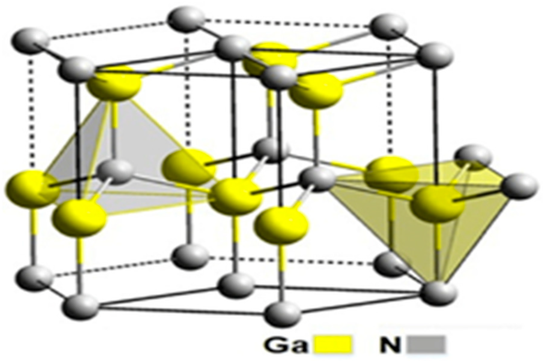
Figure 1. Wurtzite crystal structure of gallium nitride (GaN), showing tetrahedral coordination between gallium (Ga) atoms (yellow) and nitrogen (N) atoms (gray) [3,4,5].
Energies 18 06020 g001
Figure 2. This figure demonstrates the structure of a GaN-based power device in three dimensions (3D).
Energies 18 06020 g002
Figure 3. This figure shows a two-dimensional (2D) cross-sectional schematic of a GaN-based power device.
Energies 18 06020 g003
Figure 4. Radar plot comparing key material characteristics of Si, SiC, and GaN, including energy gap, breakdown field, thermal conductivity, and carrier transport properties.
Energies 18 06020 g004
Figure 5. Mission profile stress mapping for a GaN EV converter: (a) drive cycle speed/torque profile; (b) converter load factor and DC link ripple; (c) computed T j (t) with ambient/coolant overlays. Source: Author simulation using representative drive cycle, converter, and thermal parameters synthesized from published EV reliability and thermal management studies [28,34,35,36,37,38,39,40,41,42,43,44,45,46].
Energies 18 06020 g005
Figure 6. Reliability-aware derating map showing the safe operating region as a function of ambient temperature and switching frequency at a constant coolant set-point; boundaries set by the junction-temperature limit ( T j ≤ 125 °C) and a dynamic R D S ( o n ) screen. Source: Simulation and derating analysis using data trends from [38,39,40,41,42,43,44,45,46].
Energies 18 06020 g006
Figure 7. Single-phase GaN bridgeless TP-PFC, followed by LLC/CLLC DC–DC; current-shaping loop and resonant tank.
Energies 18 06020 g007
Figure 8. Schematic diagram of a Vienna rectifier topology for three-phase AC to DC conversion.
Energies 18 06020 g008
Figure 9. T-type neutral-point-clamped (NPC) rectifier, single-phase leg: GaN switches S1/S4 are the outer devices, S2/S3 clamp to DCn; node A is the phase output. The green arrows represent the external body diodes of the GaN switches.
Energies 18 06020 g009
Figure 10. Parasitic inductances in a GaN half-bridge—DC-link ESL, external loop L e x t , device/source inductances L S T I /2 and dynamic drain paths L D T I and L D T 2 , illustrating the common-source inductance path.
Energies 18 06020 g010
Figure 11. Miller-coupling path and driver remedies in an AC–DC half-bridge: split R g (firm off, shaped on), active Miller clamp, and optional negative bias if allowed (use your former paper’s schematic). The red arrows indicate the Miller-coupling current paths and charge-transfer loops between the gate, drain, and source during switching transitions.
Energies 18 06020 g011
Figure 12. Normalized LLC gain for various Q s ; ZVS to the right of f r , ZCS to the left. Source: Analytical simulation based on standard LLC resonant-tank equations and characteristic curves reported in [63,64,65,66,67,68,69]. The blue line represents the LLC resonant tank gain curve for the lowest quality factor (Qₛ = 0.1), indicating operation under the heaviest load condition.
Energies 18 06020 g012
Figure 13. DAB (SPS) normalized power P(δ) vs. phase shift with an illustrative ZVS boundary; shaded region indicates potential no-ZVS at light load. Source: Analytical modeling using phase-shift control re-lationships discussed in [67,68,69,70,71,72,73]. The shaded (blue) region indicates the potential no-ZVS operating zone at light-load conditions, where insufficient circulating energy prevents full soft-switching.
Energies 18 06020 g013
Figure 14. Scaling map for GaN LLC/CLLC/DAB: ZVS constraint (solid), thermal/magnetics limit (dashed), shaded feasible region, and indicative 400 V/800 V ranges. Source: Simulation derived from analytical scaling relationships and design envelopes summarized in [71,72,73,74,75,76,77,78,79,80,81,82,83,84].
Energies 18 06020 g014
Figure 15. (a) GaN-ready gate/loop layout for resonant DC–DC: driver adjacent to devices, Kelvin-source return, split R g , compact commutation loop, and local MLCC decoupling (insert the layout figure from your former paper). (b) Miller-coupling and immunity in resonant operation: off-gate bump vs. d v d t , role of active Miller clamp and (if permitted) negative off-bias; timing relative to tank-current zero crossings (insert your schematic/timing graphic). The red circle indicates the GaN transistor region where Miller coupling and off-gate behavior are analyzed.
Energies 18 06020 g015
Figure 16. Ferrite-assisted circular wireless power transfer (WPT) link, showing Tx and Rx coils with a ferrite shield layer for magnetic flux confinement and improved coupling efficiency.
Energies 18 06020 g016
Figure 17. Capacitive power transfer (CPT) circuit showing the coupling plates, P 1 P 4 , excitation source, U I N , and load,   R L . The LCL compensation network enables zero-phase-angle operation and efficient electric-field coupling under high-frequency GaN switching.
Energies 18 06020 g017
Figure 18. Power–frequency design-space comparison, showing GaN’s expanded operating region toward a higher switching frequency and power density relative to Si and SiC technologies, enabling compact and efficient converters for advanced EV propulsion.
Energies 18 06020 g018
Figure 19. CISPR-25 dual-LISN voltage-method bench (two 5 µH/50 Ω LISNs), showing simultaneous V + f and V f measurements for DM/CM separation: V D M = V + f V f 2 , V C M = V + f + V f 2 .
Energies 18 06020 g019
Figure 20. Dual-LISN DM/CM model and measurement: two 5 µH/50 Ω LISNs (line and return), with CM/DM paths and voltage reconstruction V CM = V 1 + V 2 2 , V DM = V 1 + V 2 2 .
Energies 18 06020 g020
Figure 21. Damped input EMI filter: series L f and shunt C f set the cutoff; C d across C I N damps resonance. V A V B mark input/output nodes.
Energies 18 06020 g021
Figure 22. Pareto/decision map—efficiency η vs. power density ρ; marker size ∝ complexity, labels show EMI margin ΔE; shaded region meets the Section 3 thermal-reliability envelope. Source: Author synthesis using analytical trade-off relations (Section 3, Section 4, Section 5 and Section 6) and the normalized literature data compiled from GaN converter benchmarks (2019–2025) summarized in Table 3 and supported by [68,71,72,73,74,75,76,77,78,79,80,81,82,83,84,85,86,87,88,89]. The yellow circle represents the T-type NPC + DAB topology, which corresponds to a design achieving an EMI margin of approximately ΔE ≈ 7 dB with a complexity factor of C = 4. This configuration demonstrates a trade-off between high efficiency (≈95.6%) and moderate power density (~25 kW/L), showing that increased circuit complexity can enhance EMI attenuation while maintaining reliable thermal performance within the defined thermal-reliability envelope.
Energies 18 06020 g022
Table 1. Comparison of key properties of Si, SiC, and GaN devices.
PropertySilicon
(Si)
Silicon
Carbide (SiC)
Gallium
Nitride (GaN)
Significance
Bandgap Energy (eV)1.13.33.4A wider bandgap enables higher temperature and voltage operation.
Breakdown Electric Field (MV/cm)0.32.83.0Higher values allow thinner drift regions and smaller devices.
Electron Mobility (cm2/V·s)15009001500Higher mobility supports faster switching.
Saturation Velocity (cm/s)1 × 10 7 2 × 10 7 2.5 × 10 7 Enables high-frequency, low-loss switching.
Thermal Conductivity (W/cm·K)1.53.71.3Affects heat dissipation efficiency.
Reverse Recovery Charge ( Q r r )HighModerate0Zero Q r r reduces switching losses and EMI.
Gate Charge ( Q g )HighModerateLowLower Q g supports fast switching with low drive loss.
Table 2. Summary of key reliability mechanisms and mitigation strategies across common GaN converter topologies.
Converter TypeStress Mechanism Typical   Δ T j (°C)Reliability ConcernRemarks/Mitigation
Synchronous Buck/BoostHigh repetitive hard-switching, asymmetric conduction40–60Dynamic R D S ( O N ) drift and hot-carrier injection at high V D S Use soft-gate drive and active snubber to minimize d v d t overshoot
Totem-Pole PFC (TPPFC)Alternating conduction between the fast GaN leg and the slow SiC/SBR leg50–70Cross-conduction and body-diode dynamic recovery heatingOptimize dead time; synchronous mode with gate-voltage shaping reduces reverse stress [152]
CLLC Resonant/Dual Active BridgeZVS/ZCS transitions minimize switching stress; thermal stress from circulating current20–40Bias temperature instability in continuous operationDesign for balanced magnetizing current; ensure minimal residual hard commutation
Vienna/T-type NPCMulti-device series paths share voltage but increase thermal imbalance risk45–65Unequal device aging, gate charge mismatchThermal coupling through the baseplate and dynamic current sharing improve lifetime consistency [153]
Bidirectional OBC/DC-link SSTHigh-frequency bidirectional power flow30–55Repetitive dynamic stress; EMI–thermal co-couplingSpread-spectrum modulation and digital THD control reduce repetitive EMI-induced heating [154]
Table 3. Comparative benchmarking of GaN-based EV converter subsystems (2019–2025): efficiency (η), power density (ρ), and EMI margin (ΔE) across representative OBC, DC–DC, and inverter implementations.
SubsystemTopology F s (kHz)η (%)Power Density
(W/L)
EMI   Margin   Δ E (dBµV Below Limit)Reference Range (2019–2025)
OBC (400 V)GaN TP-PFC + CLLC200–50096–983.5–5.0−5 to −8[46]
OBC (800 V)GaN T-Type 3L + DAB150–30095–974.2–4.8−4 to −7[169]
DC–DC StageLLC/CLLC300–100096–986.0–9.0−3 to −6[141]
Traction Inverter3-Phase GaN NPC100–20098–997.5–10−2 to −5[170]
EMI Filter BenchmarksHybrid CM/DM Filter + GaN Leg500–1000--−6 to −10[171]
Table 4. Quantitative roadmap targets for GaN-based EV converter subsystems at 400 V and 800 V platforms.
SubsystemPlatformTopology Band (Favored) F s (kHz)Target η (%) Target   ρ
(W/L)
Target Δ E (dBµV) Thermal   Headroom   H t h
OBC AC-DC [46]400 VTP-PFC → LLC/CLLC150–400 kHz≥97.5%≥4.5≤−6 (150 k–30 MHz)≥15 °C at T C o o l ,   i n = 15 °C
OBC AC-DC800 V [173]3L Vienna/T-type NPC120–300 kHz≥97.0% (Vienna), ≥96.5% (T-type)≥4.2≤−5≥12 °C
Isolated DC-AC [174]400 VLLC/CLLC, DAB300–900 kHz≥97.8% (peak), ≥97.0% (rated)≥6.5≤−6≥15 °C
Isolated DC-AC [175]800 V3L-LLC/CLLC or DAB250–700 kHz≥97.2%≥5.8≤−5≥12 °C
Traction Inverter [176]400 V3-phase NPC (GaN)60–150 kHz≥98.8%≥8.0≤−3 (DM bands; CM shaping)≥10 °C
Traction Inverter [177]800 V3-phase NPC (GaN, stacked/3L)50–120 kHz≥98.3%≥7.0≤−3≥10 °C
Disclaimer/Publisher’s Note: The statements, opinions and data contained in all publications are solely those of the individual author(s) and contributor(s) and not of MDPI and/or the editor(s). MDPI and/or the editor(s) disclaim responsibility for any injury to people or property resulting from any ideas, methods, instructions or products referred to in the content.