Article

Modeling of Residual Stress, Plastic Deformation, and Permanent Warpage Induced by the Resin Molding Process in SiC-Based Power Modules

1
Department of Civil Engineering and Architecture, University of Catania, Via Santa Sofia 64, 95123 Catania, Italy
2
Department of Electrical, Electronic and Computer Engineering, University of Catania, Via Santa Sofia 64, 95123 Catania, Italy
*
Author to whom correspondence should be addressed.
Energies 2025, 18(20), 5364; https://doi.org/10.3390/en18205364
Submission received: 30 July 2025 / Revised: 4 October 2025 / Accepted: 5 October 2025 / Published: 11 October 2025

Abstract

A critical aspect in the design of power electronics packages is the prediction of their mechanical response under severe thermomechanical loads and the consequent structural damage. For this purpose, finite element (FE) simulations are used to estimate the mechanical performance and reliability under operational conditions, typically alternate high voltages/currents resulting in thermal gradients. When simulations are performed, it is common practice to consider the as-received package to be in a stress-free state. Namely, residual stresses and plastic deformation induced by the manufacturing processes are neglected. In this study, an advanced FE modeling approach is proposed to assess the structural consequences of the encapsulating resin curing, typical in the production of silicon carbide (SiC)-based power electronics modules for electric vehicles. This work offers a general modeling framework that can be further employed to simulate the effects of thermal gradients induced by the production process on the effective shape and residual stresses of the as-received package for other manufacturing stages, such as metal brazing, soldering processes joining copper and SiC, and, to lower extents, the application of polyimide on top of passivation layers. The obtained results have been indirectly validated with experimental data from literature.

1. Introduction

Power electronics components play a key role in the energy transition, in particular in the automotive sector [1], rail systems [2], and renewable energies [3]. Electronic modules are typically made by combining different layers of dissimilar materials, mainly metallic, polymers, and ceramic [4], all of which present different mechanical and thermal properties. Under normal operative conditions, power modules undergo severe thermomechanical loads induced by the large amount of electrical power [5]. Then, in these multi-laminar systems, thermomechanical stresses, residual local plastic deformations, and warpage phenomena arise [6,7], resulting in loss of performance and reduced lifetime. Indeed, the mismatch of thermal expansion coefficients and mechanical properties can result in thermal deformations, delamination, and, eventually, failure [8,9].
Passive thermal cycling and active power cycling are the most widely used experimental methods for testing the reliability of the modules [10]. Furthermore, finite element (FE) simulations are largely used to predict performance and reliability under operative conditions [11]. However, in simulations it is common practice to assume that the module is in a stress-free state at room temperature before applying external loads [11,12,13], neglecting the residual stresses and plastic deformations induced by the manufacturing process. In reality, these have a significant impact on reliability and lifetime. They can lead to warpage, delamination, or cracking, thereby reducing structural and electrical performance. Proper characterization is therefore essential to optimize processes and materials. In this regard, in [6] the initial state of the package at room temperature, showing residual pre-stresses and pre-strains due to the production processes, was modeled considering that the component was undeformed and unstressed at a conventional “stress-free temperature”, different from room temperature. Then, the external thermomechanical loads were superimposed on the approximate production-induced pre-strains and pre-stresses. Similarly, Dudek et al. [9] modeled the delamination phenomenon in power packages subjected to thermal cycles, assuming a stress-free condition at a temperature of 175 °C. Zhu et al. [7] studied residual stresses and warpage in a bilaminar copper–glass component. The authors experimentally measured the warpage induced by the production process and calculated the residual stress based on the sample curvature. Struzziero et al. [14] studied resin transfer, modeling curing effects on residual stresses and warpage of a resin–glass fiber bilamina. They showed that processing time strongly influences residual stresses and final shape and suggested engineering them through cure cycle design to counteract cooldown stresses. Gschwandl et al. [15] studied residual stresses from the epoxy molding compound encapsulating a D2PAK power package, modeling curing kinetics with the Prout–Tompkins model and the Cure Hardening Instantaneous Linear Elastic (CHILE) approach [16,17]. In CHILE, resin stiffness evolves from negligible (uncured) to increasing (curing) to plateau (fully cured). Results in [15] link residual stresses and plastic deformation mainly to manufacturing and thermal mismatch between resin and metallic parts.
This work presents an advanced FE modeling approach to assess manufacturing effects (resin solidification, stiffness variation, adhesion) on a representative SiC-based power module, similar to those analyzed in [6,15,18]. Epoxy resins evolve irreversibly during curing as polymer chains crosslink [14,15]. The model includes elastoplastic nonlinear behavior of the materials, often neglected, capturing resin property changes during molding and their impact on stresses, plastic strains, and warpage of the package. Resin molding may be taken as representative of other processes, such as Cu–SiC soldering or polyimide deposition, where layered materials with different properties lead to residual stresses and deformation. No specific experimental data is available due to the general representativity of the package and industrial confidentiality. However, the obtained results have been indirectly validated with experimental data from literature [19]. Moreover, the modeling strategy (post-yield response, layer contact, mesh sensitivity) was already validated in a previous work with less sensitive experimental data freely available [20].
Summarizing, the novelty of the present work lies in the innovative approach for evaluating a representative step of the manufacturing process of power electronics packages, namely the resin molding process, which includes the nonlinear behavior of materials and an accurate simulation of the mechanical interaction between the encapsulating resin and the underlying layers during the resin curing process.
The paper is organized as follows. Section 2 presents the main features of the power electronic components. Section 3 describes the FE modeling approach used to simulate thermal gradients during solidification, stiffness transition, and resin adhesion to package components. Section 4 discusses numerical results on stress distributions, residual stresses, plastic deformation, and warpage. Finally, Section 5 provides the summary and conclusions.

2. SiC-Based Module and Modeling Process

2.1. SiC-Based Power Module

Silicon carbide (SiC) semiconductors are growing in popularity. In particular, SiC-MOSFETs offer huge potential for power electronics due to their reduced conduction and switching losses and ability to withstand higher junction temperatures. The main components included in these systems are semiconductor dies made of SiC. By means of solder alloys, the dies are attached and interconnected to the underlying copper–ceramic–copper substrate, which forms an electrical circuitry on the top layer and provides a good thermal exchange on the bottom layer. Finally, in order to insulate all the electronic devices and protect the layers subjected to oxidative and corrosive phenomena, the entire system is usually encapsulated within epoxy resin [21].
The modeled package is representative of a commercial SiC-based power module for automotive applications [22].
However, it includes dimensional and shape modification with respect to the reference packages for being comparable to experimental data from the literature and for preserving the industrial confidentiality.
The multilaminar assembly considered in this study consists of different material layers, all of which present different mechanical and thermal properties. The chosen configuration (Figure 1a) is made of a copper-ceramic-copper Active Metal Brazed (AMB) substrate in which a silicon nitride layer (Si3N4 or SiN briefly) is bonded to two copper layers, solder layer (PbSnAg) that electrically connects the top copper layer of the AMB substrate with the upper SiC layer, a double passivation layers formed by TEOS (tetraethyl orthosilicate) and SiN deposited onto the SiC upper surface, a layer of polyimide accommodating for the thermomechanical solicitations [11], and finally a thermosetting resin that encapsulates the whole multilaminar package. Slightly different configurations of the targeted components can be found in [23]. The passivant layers, as TEOS, SiN, and polyimide layers, present a frame shape as shown in Figure 1b. During the manufacturing process, the inner empty space inside the three aforementioned layers is filled with resin, indicated as internal resin in Figure 1b.

2.2. Molding Process

Simulating the thermomechanical stresses, residual plastic deformation, and shape changes (warpage) induced by the curing of the resin requires a more advanced modeling approach than the simple adoption of a “stress free” temperature method.
Here the simulation strategy includes the definition of the molding temperature history, the transition of the resin stiffness, and the adhesion between the resin and all the surfaces in contact with it, together with other simulation details accounting for the preliminary molding phase where the resin is fluid. Then, the proposed procedure enables the simulation of the progressive mechanical interaction of resin and package under variable temperature, from their initial state of mechanically uncoupled solid-fluid bodies free to independently move–expand–deform, to their final state of fully coupled solids, which can only move–expand–deform as a single non-homogeneous body.
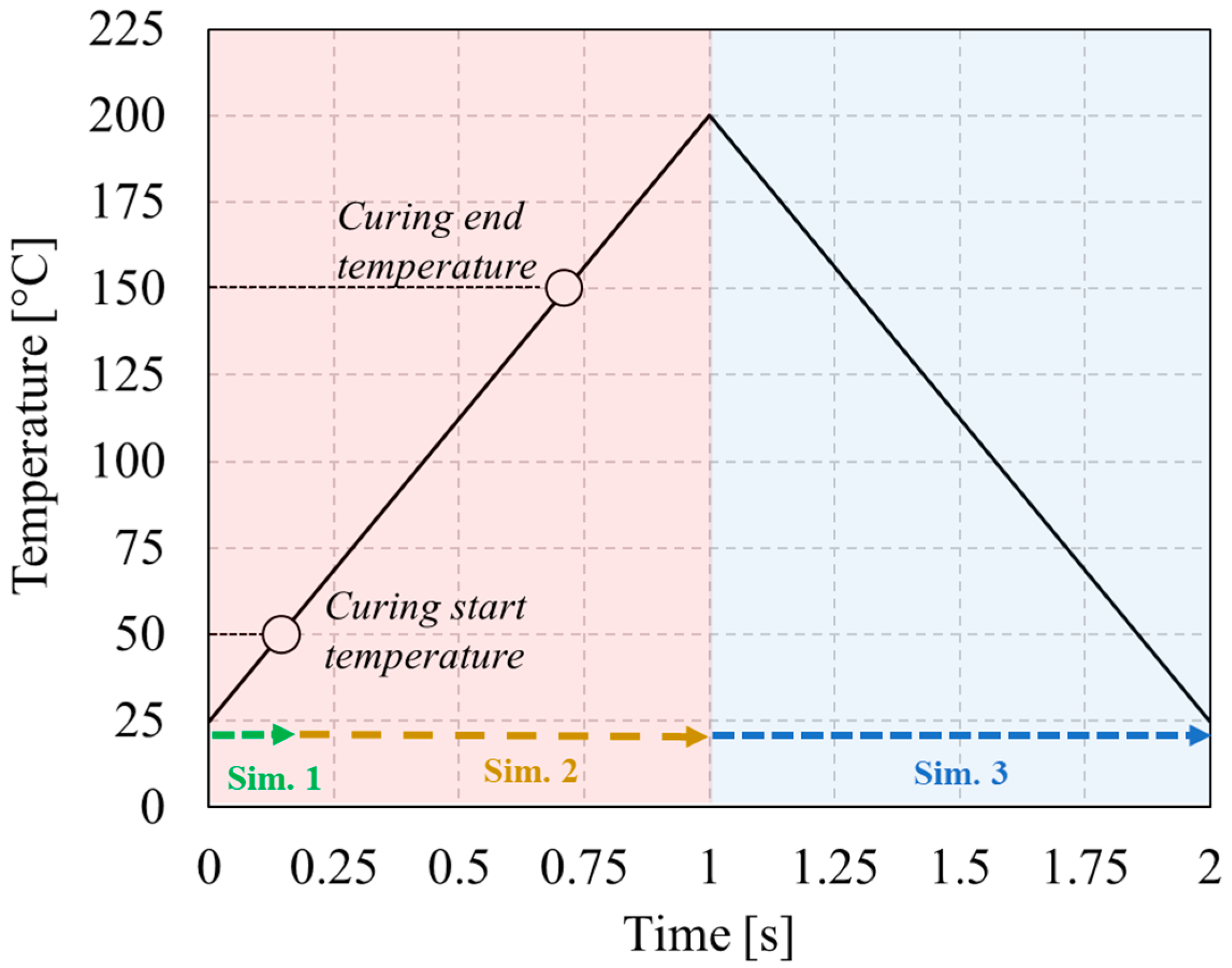
The manufacturing stages prior to the resin molding are assumed to be complete, so the AMB substrate supporting the soldered SiC die, and the three passivants of TEOS, Si3N4, and polyimide are considered to be already a single semi-finished multi-layered body. This partially assembled structure is also named “Copper-to-Poly” assembly for brevity. In the molding process here considered, the resin is firstly preheated up to a representative temperature of 50 °C to flow into the mold. The preheated resin, in the state of a viscous fluid, is pressurized into the mold where it fills all the space and is pushed against its mating surfaces, namely the upper copper layer of the AMB substrate, the SiC on top of it, and the polyimide. The viscous resin starts to adhere to the above surfaces while it is still fluid and has negligible stiffness/elastic modulus. As the mold is full and pressurized, the temperature gradually increases up to 200 °C. Slightly above the 150 °C temperature of complete curing of the resin. A final cooling phase from 200 °C to 25 °C follows. Figure 2 shows the considered temperature cycle vs. time (the time scale is arbitrary as no rate–effect are modeled). The simulation strategy (see arrows in Figure 2) will be further clarified in the next section. During the heating phase, the whole assembly goes through thermomechanical loadings of two interacting types.
The first type of thermomechanical load is due to the simple heating of the assembly “Copper-to-Poly” during the pre-heating phase, until 50 °C, where such assembly deforms and is stressed due to its own heterogeneous multi-layered nature, but its deformation/stress states are not affected by the still-fluid resin.
Then in the second heating phase beyond 50 °C, the curing resin progressively solidifies and increases its elastic modulus, gradually introducing more and more intense constraints to the deformation of the copper-to-poly assembly, until the temperature of 150 °C is reached. At 150 °C, the solidification is complete, and the assembly becomes a single structural solid body. Beyond 150 °C, the resin stiffness does not change any further. Then in the final part of the heating phase, from 150 °C to 200 °C, as well as in the successive cooling phase down to 25 °C, the thermomechanical loading history is applied to a “new-born” structural component which is already pre-loaded and pre-strained due to the previous stages of the molding process.
It is worth noting that, in the FE simulation, the time scale shown in Figure 2 is purely arbitrary, since a quasi-static implicit solver, free of any rate-dependent or transient effects, was adopted. In particular, the evolution of the resin stiffness depends solely on the imposed temperature, which is applied uniformly to the entire package volume without any delay or spatial gradient.

3. Modeling Strategy

3.1. Mesh, Material and Boundary Conditions

Numerical simulations of the resin molding process are performed by the commercial FE code MSC Marc®. Only a quarter of the assembly is modeled thanks to the symmetries. A schematic representation of the meshed assembly is given in Figure 3. The resin volume above the polyimide layer (External Resin in Figure 1b), the AMB substrate, and SiC are modeled using full integration eight-node, isoparametric, hexahedral solid elements (SE) (Hex 7 in Marc), while solder, passivants (TEOS, SiN, and polyimide), and internal resin are modeled using solid shell elements (SSE) having eight-node brick topology and shell formulation (Hex 185 in Marc). This modeling choice allows a better definition of the contact between the different layers as well as a better discretization of the resin mesh. The mathematical formulation of the solid shell element includes integration points through the element thickness in order to capture the material response under bending load. This element definition is particularly suitable in the case of solids in which the in-plane dimensions are much greater compared to the through thickness one, but planar quad-elements are not accurate enough or do not allow dual-face contact interactions.
A glued-type contact interaction is considered between each couple of neighboring layers. Indeed, the imperfect bonding between layers in a power electronic package was analyzed in [20], showing that no relevant changes in the stress–strain distributions occur as far as the debonding area is limited to the realistic size of such manufacturing imperfections. Instead, the delamination–damage of similar packages, analyzed in [24], was found to affect the stress–strain distributions within the package only after the onset of damage evolution is triggered by stresses and plastic strains beyond certain thresholds. Therefore, the glued-type bonding conditions simulated in the present work are suitable to deliver realistic predictions until no damage evolution initiates and eventual bonding defects from manufacturing start progressing.
Finally, a rigid plane with touching contact is modeled at the base of the module in order to prevent its vertical rigid-body motion without constraining its deformation displacements. The relative simplicity of the body’s geometry allows for manual meshing (no auto-meshing), which guarantees controllable element aspect ratios (see also Figure 3).
The overall model counts 64,570 elements and 75,629 nodes. Table 1 compiles the dimensions of each component as well as details on the mesh used for their discretization, i.e., element type, number of elements, and minimum element size.
The meshing features adopted here (mesh sizes, subdivisions of layer thickness, aspect ratios, and a model zones where to adopt refined/coarser meshes) complied with the knowledge previously acquired in [20], where a global-local approach demonstrated the suitability of the opportune global mesh to fairly reproduce the mechanical response of the assembly beyond the disturbances of mesh sensitivity.
That paper showed that an appropriate mesh size, suitable for globally modeling the whole package, can provide results to be used as boundary conditions for smaller-size local models with ten times finer meshes, leading to successfully capturing discontinuities and large stress–strain gradients in sub-volumes of interest within the package, without extending the finer meshes all over the entire package and, so, limiting the computational burden of the analysis.
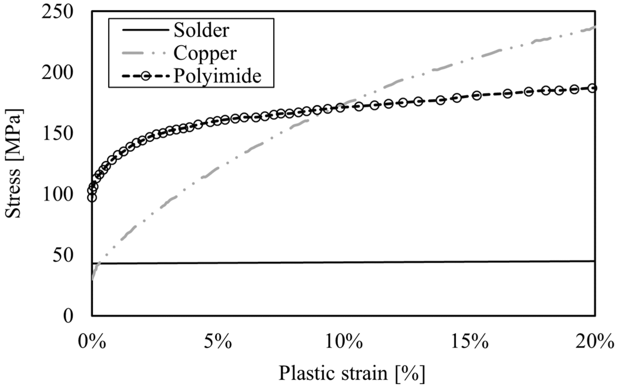
The temperature history given in Figure 2 is uniformly imposed all over the entire model. All materials are modeled as purely elastic bodies according to the data reported in the literature [25,26,27,28,29,30], with the exception of copper, solder, and polyimide, which are considered to be elastoplastic according to the representative hardening curves shown in Figure 4. For the latter elastoplastic materials, the adopted model is the classic Von Mises plasticity combined with isotropic hardening. Considering the plasticity of the materials involved is a key innovative aspect of the present work, as it is commonly completely neglected in the literature. Elastic constants, mass density, and coefficient of thermal expansion for all materials, considered at room temperature, are listed in Table 2. These characteristics are assumed temperature-independent, as commonly performeddone in the literature [7]. However, this approximation may affect the results, but it does not compromise the innovativeness of the proposed approach, as discussed below. Note that each material in the package exhibits a different coefficient of thermal expansion (see Table 2). Namely, each material will tend to deform differently during heating. As well documented in the literature [8,9], such mismatch can generate shear stresses, promote delamination, and ultimately lead to failure.
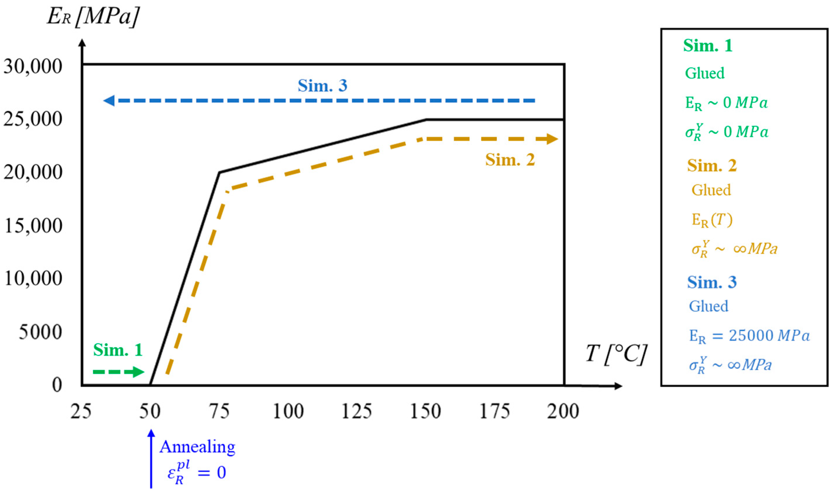
Table 2. Elastic constants, mass density, and coefficient of thermal expansion for all materials considered at ambient temperature. * The elastic modulus of the resin is considered variable with temperature in the heating stage according to Figure 2 and Figure 5 and constant in the cooling stage. Resin’s volumetric contraction due to polymerization is here neglected.
Mass
Density
Young’s
Modulus
Poisson’s
Ratio
Thermal Expansion Coefficient
[tonnes/mm3][MPa][-][1/°C]
Resin (cured)1.21 × 10⁻⁹ 25,000 *0.341.20 × 10−5
Copper8.96 × 10−9125,0000.31.75 × 10−5
Solder6.54 × 10−956000.42.90 × 10−5
SiC3.21 × 10−9410,0000.284.00 × 10−6
TEOS1.04 × 10−959,0000.251.00 × 10−6
SiN3.17 × 10−9300,0000.293.40 × 10−6
Polyimide1.15 × 10−930000.345.00 × 10−5
Figure 5. Schematic representation of the development of resin stiffness during a thermal cycle. The thermal cycle is subdivided into three different simulations indicated by arrows. A zeroing of plastic strain of the resin takes place at the end of the first simulation.
Energies 18 05364 g005
As concerns the resin, as previously mentioned, its mechanical behavior is strongly linked to the initial curing and end curing temperatures [16,17] (see also Figure 2). Therefore, an advanced modeling strategy accounting for the variability of the resin stiffness is adopted here and further described in detail.

3.2. Three-Stages Analysis for Resin Curing

The complex mechanical interaction of the copper-to-poly solid assembly with the adhering resin subjected to fluid-solid phase change was approached by subdividing the simulation of the whole molding process into three distinct analyses where the deformed/stressed model resulting from an analysis constitutes the input to the successive one, according to Figure 5. This split of the analysis was necessary to insert modifications to the model between an analysis and the successive one, reflecting the actual changes in the physical state/features of the resin.
In the first analysis (Sim. 1 indicated by the green arrow in Figure 2 and Figure 5) the resin is assumed to be a purely elastic/perfectly plastic solid with negligible yield stress and elastic modulus. Hence, in the first analysis, the modeled resin follows the thermal deformation of the copper-to-poly assembly without opposing significant resistance, closely mimicking what the fluid resin does in the real molding process. It is important to note that in this simulation stage, the extremely low yield stress assigned to the resin allows us to ensure that it only accumulates plastic strains almost without elastic strains. Such plastic deformation is then zeroed at the end of the first analysis so that the strain history of the resin during its fluid phase is reset.
It might be argued that the resin in Sim. 1 could be simply modeled as a purely elastic material with extremely low stiffness, but preliminary simulations proved that this approach generates large elastic strains that cannot be reset (the zeroing only acts on the plastic strain component) and would remain “sleeping” (without inducing any relevant stress) as far as the elastic modulus of the resin remains negligible in the fluid phase but would “awake” (generating unrealistic very high stresses) as the elastic modulus of the resin increases in the successive stages of the curing process simulation.
Therefore, the first stage of the modeling strategy proposed here allows us to reproduce a fully realistic pre-heating phase with the resin modeled as a solid but mimicking the structural interaction of a viscous fluid, in fact:
-
At 50 °C the resin is completely stress-free while the “Copper-to-Poly” assembly is not in a stress-free condition.
-
the resin is stretched-deformed following the deformed shape of the “Copper-to-Poly” assembly, but it is not generating any stress nor is it storing any elastic strain which would generate unrealistic stresses in the successive simulation stages.
In the second simulation phase (Sim. 2 indicated by the yellow arrow in Figure 2 and Figure 5), the temperature is increased from 50 °C (curing-start temperature) to 200 °C. Now the resin is simulated as purely elastic material (very high yield stress) with Young’s modulus evolving according to the reference curve of Figure 5. Note that, in Sim. 2, the elastic modulus evolves gradually together with the temperature, which triggers the progressive build-up of possible relative deformation between different layers and, consequently, the gradual continuous development of internal pre-stresses and pre-strains. The temperature of 150 °C is assumed to be the curing-end temperature, at which the solidification of the resin is completed, and its elasticity modulus reached the final value, maintained constant for the rest of the simulation. At this stage the “birth” of the power electronics assembly in its final form is completed, as no further changes in its physical properties can occur.
If the elastoplastic properties of copper, solder, and polyimide are properly taken into account, then the newborn assembly model can predict permanent deformations and residual stresses arising in the successive thermal load history, which includes a further post-cure heating up to 200 °C and the successive cooling down to room temperature, in addition to those eventually cumulated already during the pre-heating stage up to 50 °C and the curing stage up to 150 °C.
The further increase up to 200 °C reflects an actual practice to ensure that all the resin volume is molded, also in peripheral/colder zones of the mold.
The third analysis finally simulates the cooling phase (Sim. 3, indicated by the blue arrow in Figure 2 and Figure 5), from 200 °C to 25 °C, where the assembly does not undergo further changes in its mechanical properties while it can undergo further plastic straining. Then, in Sim. 3, the elastic modulus of the resin is fixed to its constant value reached at 150 °C, independently of the decreasing temperature imposed on the model. As a further finesse, a temperature-dependent modulus might be implemented referring to the fully solidified resin, but this modulus variability is orders of magnitude smaller than that of the pre-to-post molding modulus and, therefore, is not considered here. Only irreversible strains and stresses are accumulated by the assembly during Sim. 3, leading to its final state.
Regarding the volumetric contraction of the resin, it initiates while the resin is not yet solidified; therefore, it has still negligible stiffness and is still unadhered to the package. Under such circumstances the contraction of the resin is unconstrained; therefore, it has no influence on the stress–strain state of the package itself. It is acknowledged that volumetric contraction might still continue until the last stages of the polymerization, when the stiffness of the resin is increasing and its adhesion to the package is progressively taking place, but such a final part of the phenomenon just corresponds to a fraction of the total volumetric contraction, and it is assumed to not change the generality of the outcomes discussed here.

4. Results and Discussion

The thermomechanical model presented in Section 2 allows us to reproduce the interplaying changes in structural features and thermomechanical loading modes occurring together during the solidification process of the resin. It is important to highlight that the results shown do not have an experimental counterpart, as the model represents a commercial device, and the related data are protected by industrial secrecy.
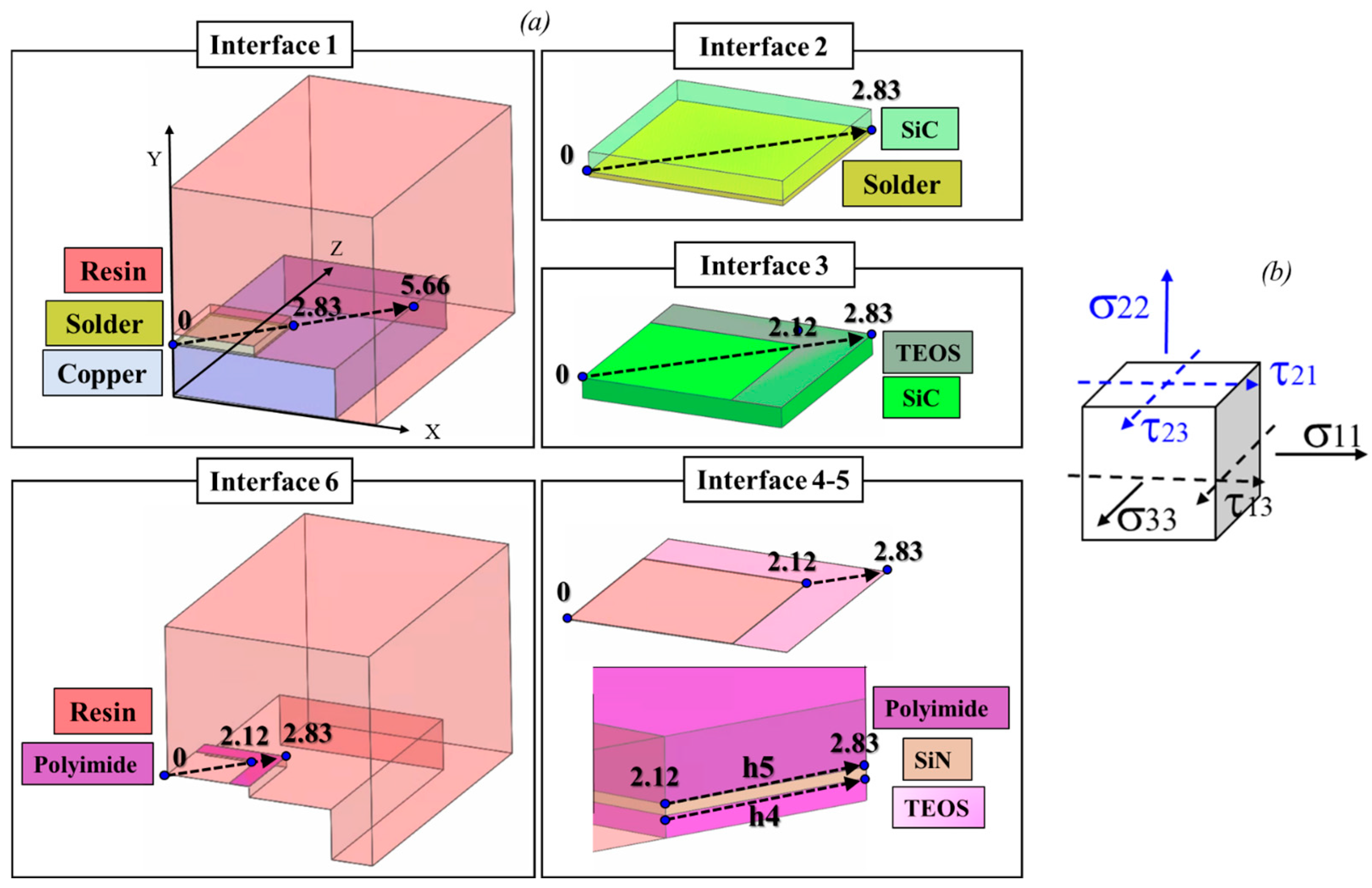
All interfaces taken in the exam are shown in Figure 6a. Stress state and residual plastic strain are extracted along the paths indicated by the black dashed arrows.
The remarkable variability in the thickness of different layers typical of power modules would require extremely fine mesh sizes for achieving detailed numerical results, at the expense of the computational cost. Alternatively, a global-local modeling approach can offer a solution here [18]. Therefore, the results reported here are representative of the overall trend of the interlaminar stress–state and plastic strain.
Figure 6b gives a schematic representation of all considered stress components, where the plane of the interfaces and of the whole assembly is xz. The blue arrows, representing one stress σ 22 and two shear stresses τ 21 , τ 23 , refer to the interface between two neighboring layers. Namely, they are the common stress components identical in both the materials of the interface at hand. These stress components are the main ones responsible for the onset of possible interlaminar damage. Moreover, in the case of symmetric assembly, the two shear stress components along the considered path are identical (in absolute value). On the other hand, the remaining stress components, two normal stresses σ 11 and σ 33 , and one shear stress τ 13 , act on the specific material and exhibit different values for the two materials, being discontinuous at each interface. Namely, they differ depending on the properties of each considered material, below and above the interface, according to the mechanical properties of the material itself. These stress components are not responsible for the loss of adhesion and interlaminar failure. On the other hand, they are associated with the possible onset of damage in the bulk materials, just below or above the considered interface. Noteworthy, the symmetry of the package makes the two normal stress components along the considered paths equal to each other, i.e., σ 11 = σ 33 . In the next sections, all stress components are quantified along all paths at the maximum temperature and at the end of the cooling phase, namely at 200 °C to 25 °C, respectively. Next, the residual plastic deformation at 25 °C on copper, solder, and polyimide is quantified and discussed. Finally, the onset of out-of-plane displacement (warpage) at 200 °C as well as at the end of the production process (residual warpage) is presented.

4.1. Stresses at Different Interfaces at the Peak Temperature

Figure 7 shows all stress components along all paths at each single interface (see also Figure 6) at the peak temperature of 200 °C. Each row refers to a specific interface, while each column refers to the evolution of different stress components. Namely, the first column shows the common stresses at the specified interface ( σ 22 , σ 21 , σ 23 blue arrows in Figure 6b). The second column gives the stress acting on the material below the interface, and the third column gives the stresses above the interface ( σ 11 , σ 33 , σ 13 black arrows in Figure 6b).
In order to provide the complete overview of the stresses on the critical zones of the whole assembly, common scales are adopted in the plots of Figure 7, highlighting the positions and orders of magnitude of stress peaks at the expense of the detailed values in less-stressed zones. The most stressed layer at 200 °C is the SiC, as the die is the stiffest component of the stack. However, the stress magnitudes of each layer should be compared to the limit stresses or other failure-related properties of the corresponding materials in order to discuss their effectiveness in promoting the risk of failure.
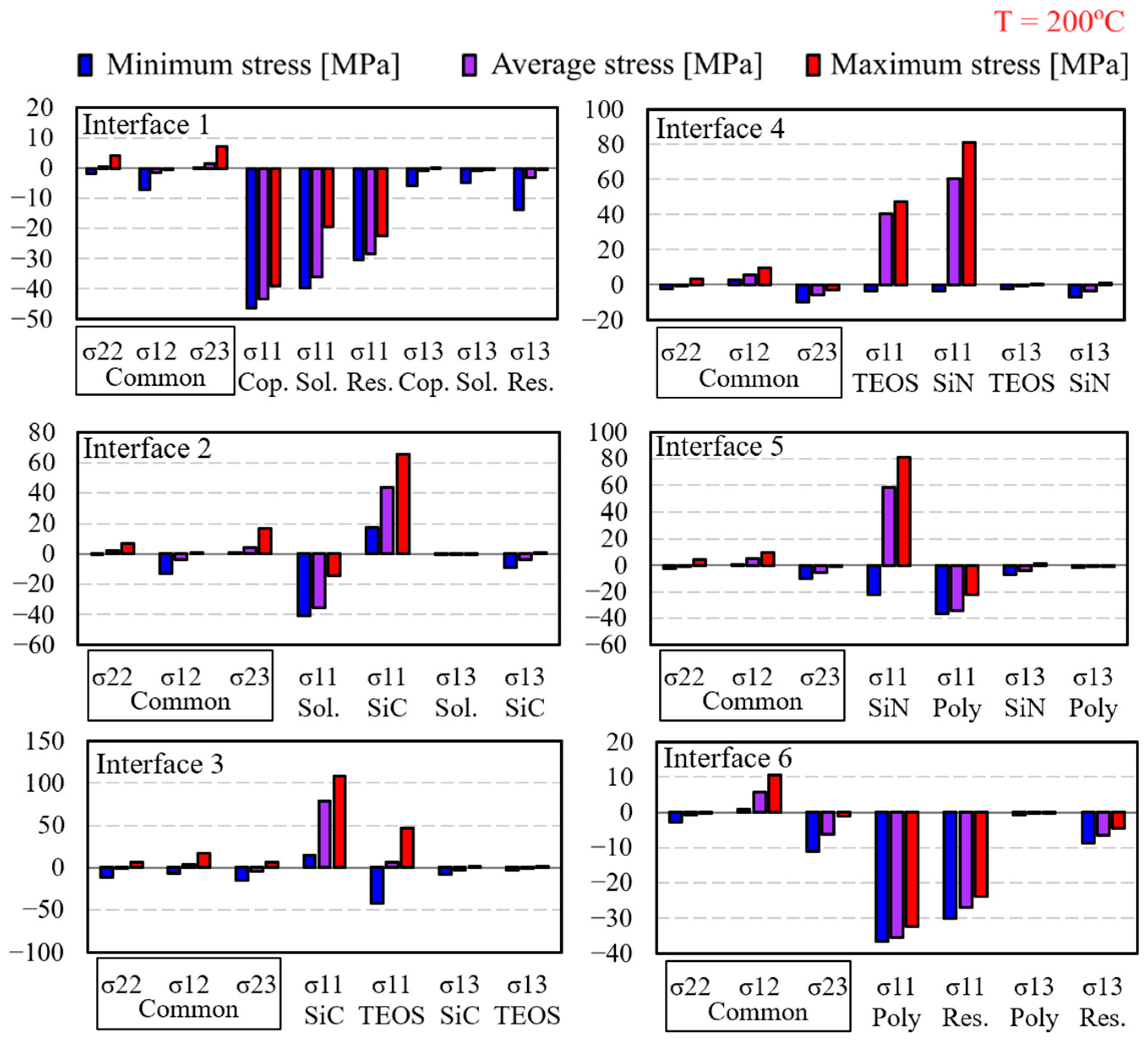
Additionally, for better readability, maximum, average, and minimum stresses for each interface are summarized in Figure 8. Note that the stress–state at 200 °C is representative of the most critical condition that the targeted assembly undergoes during the manufacturing process, i.e., maximum thermal expansion giving rise to high values of stresses. The predicted maximum (in absolute value) stresses at each interface are further discussed and compared to values of maximum tensile/flexural stress/strength, or, when possible, stress at fracture, from the literature.
In [32], the authors reported tensile stress–strain curves for copper sheets produced via different processes, namely without any annealing, with annealing and free cooling, and with annealing attached to ceramic during cooling. This last configuration was employed to produce a combined copper-ceramic material similar to the one considered in this study. In the case of copper without any annealing, the uniform and fracture stress are both close to about 330 MPa (almost flat stress–strain curve). In the second case, the free-annealed material presents lower fracture stress of about 250 MPa but larger ductility (almost 30% of uniaxial deformation). The last copper given in [32], similar to the one used in power electronic applications, presents lower fracture stress and ductility, about 155 MPa and slightly above 15%, respectively. In the FE simulation, the greatest tensile stress is found at Interface 1, and, in particular, at the copper–solder interface, i.e., σ 11 = 42 MPa . In [33], the authors investigated the mechanical properties of Sn-Pb-based solder joints used for electronics components. They reported a failure stress in tension between 60 and 80 MPa, while in the FE model, the maximum stress found at the solder interface is σ 11 = 38 MPa . Similarly, according to the data given in [29], the ultimate tensile strength is 52 MPa. Even though the ultimate tensile strength does not directly give an indication of the failure stress, it suggests that also at the maximum temperature, the material still remains in the uniform deformation regime and no stress/strain localization takes place. It must be noticed that the material showing the greatest maximum (in absolute value) stress is the SiC. Particularly, the Interfaces 2 solder-SiC and 3 SiC-resin (maximum tensile stress on SiC σ 11 = 70 MPa and 100 MPa , respectively) might be the most critical ones for the reliability and lifetime of the considered power electronic component. According to the work of [34], the alpha-SiC tensile strength at room temperature was found to vary between 180 and about 270 MPa. On the other hand, the flexural strength obtained testing the material in four-point and three-point bending at room temperature was reported to vary between about 330 and 400 MPa. The comparison between the experimental data reported in [34] and FE results puts into evidence that the manufacturing process itself might trigger the onset of damage in the SiC layer at the solder-SiC interface, and therefore, induce a consequent loss of performance of the whole component. To the authors’ knowledge, no mechanical properties of the TEOS are available in the literature, and no reference data are available for comparison with FE results. However, it is worth reporting a moderate maximum tensile stress from FE, σ 11 = 47 MPa , and almost negligible shear stress. Several studies focused on the mechanical behavior of SiN (Si3N4) during dynamic cycles (fatigue), as well as performing creep experiments [35]. Concerning its quasi-static behavior at room temperature, in [36], the authors reported a tensile strength varying between 500 and 700 MPa. Note that in the FE simulation at the maximum temperature, this material reaches a maximum stress σ 11 = 82 MPa . In [37], the authors compared the flexural strength of several types of polyimide, reporting values varying between 65 and about 80 MPa. At the maximum temperature, the maximum normal stress acting on polyimide was found σ 11 = 36 MPa , while the shear stress τ13 is negligible. However, at the Interface 6 (polyimide–resin), a maximum common shear stress τ 12 = 10 MPa is found. For the resin, according to data from the literature [27], the ultimate tensile strength can vary between 14 and 300 MPa depending on the production process. In [38], the authors investigated the tensile strength of epoxy resin in uniaxial tension. The authors reported values of maximum stress ranging between 30 and 45 MPa. As it is visible from the plot in Figure 8 (Interface 6 polyimide–resin), the maximum compressive stress acting on the resin is σ 11 = 30 MPa . On the other hand, the maximum common shear stress is τ 12 = 10 MPa (responsible for the eventual onset of interlayer delamination). Despite the high variability of the resin mechanical properties depending on the specific production parameters, i.e., temperature and pressure, FE results put into evidence that Interface 6 can be identified as a critical interface for the onset of interlaminar failure. It is important to bring to the readers’ attention that the experimental characterization of the interface fracture performance (with respect to mode I and mode II) requires challenging experimental campaigns. Indeed, each interface might behave differently depending on the two joint materials, as well as on the manufacturing joining technology. In this regard, despite the difficulty to experimentally validate and compare the obtained results, FE simulation represents a powerful tool to perform first-order analysis on the interlaminar stress distribution, which can be used to select and improve the joining operation.

4.2. Residual Stresses and Plastic Deformation at the End of Cooling

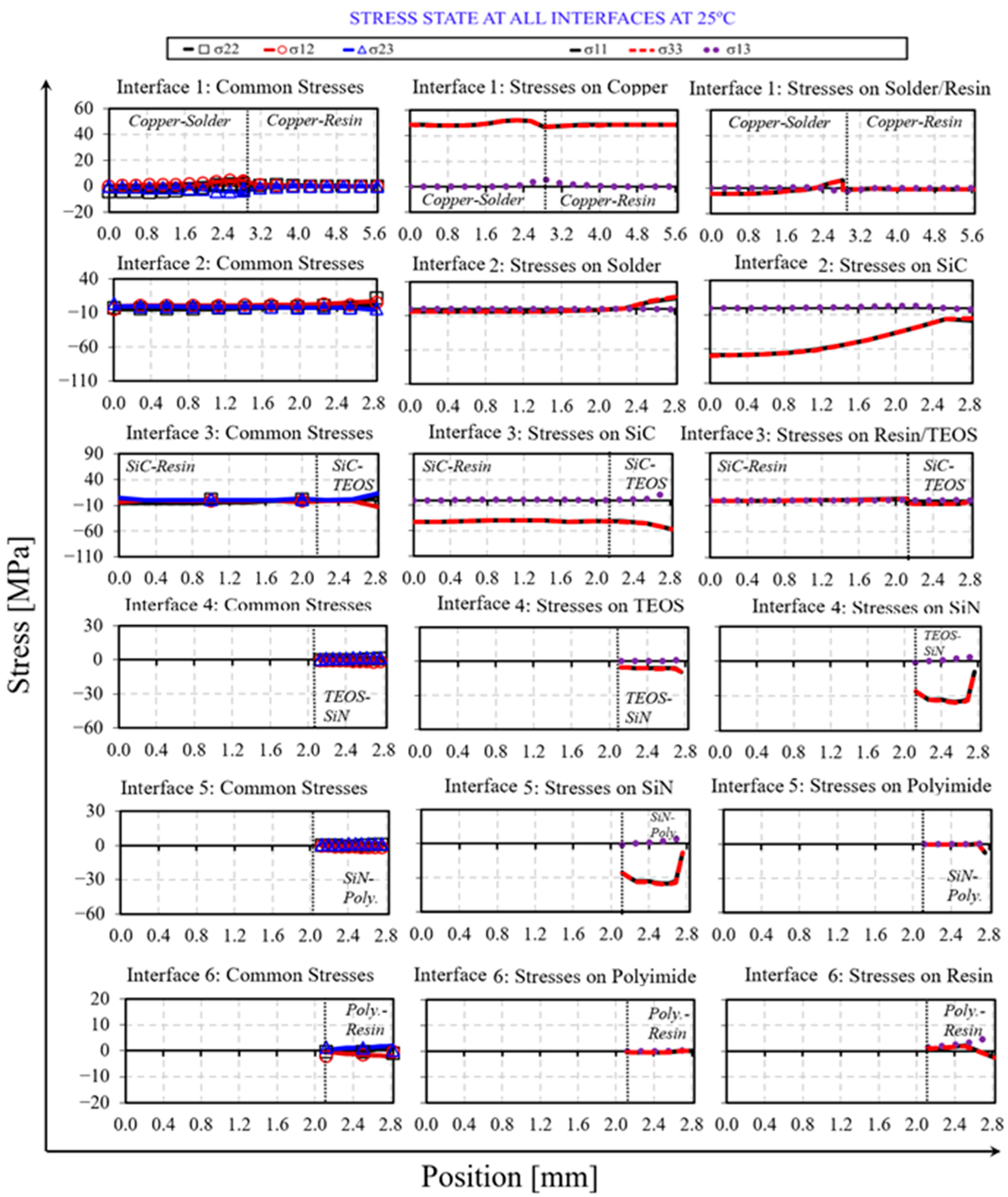
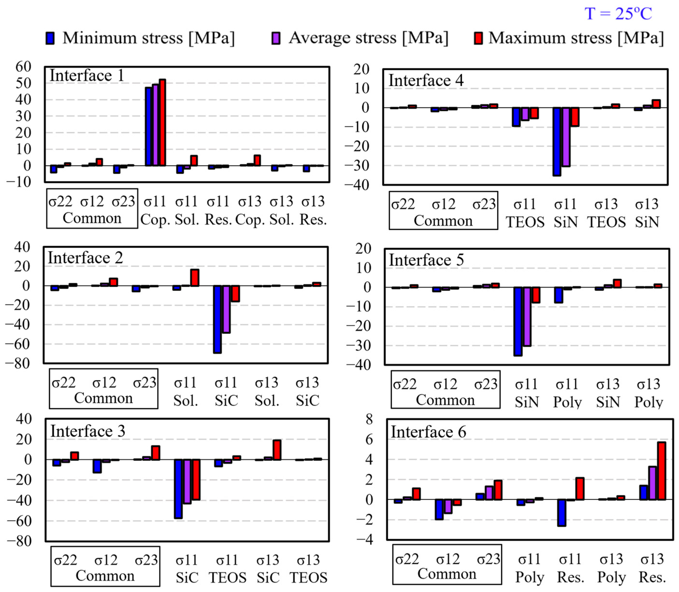
Figure 9 shows all the stress components along all paths at each single interface (see also Figure 6) at the end of cooling, T = 25 °C. Additionally, for better readability, maximum, average, and minimum stresses for each interface are summarized in Figure 10.
Both figures are representative of the stress distribution at each layer at the end of the manufacturing process and clearly show that the final component presents significant residual stresses. It is worth bringing to the reader’s attention that in the case of reliability analysis including fatigue life and thermomechanical numerical and experimental investigation, power electronic components, such as the one presented in this study, are commonly considered undeformed and unloaded. On the contrary, FE results highlight that, due to the elastoplastic behavior of the materials inside the multilaminar component, the manufacturing heating–cooling cycle is not reversable, and in addition, it gives rise to residual stresses. By comparing the graphs of the stress distribution at the interfaces at 200 and at post-cooling 25 °C, it is possible to notice that most of the stress components change their sign. For instance, at the maximum temperature, the copper is mainly subjected to compressive stresses, while at 25 °C it is subjected to tensile stress. Similarly, the resin is subjected to compressive stresses at 200 °C, while it is almost stress-free at 25 °C.
It is important to underline that, at each interface, during the heating, the layers with higher CTE tend to be compressed and those with lower CTE tend to be stretched, as the mutual competitive interaction between both layers causes the former expansion to be reduced and the latter to be increased. Permanent deformations of plastic layers further interact with this general response.
It is clear that without properly modeling the elastoplastic response of copper, solder, and polyimide layers, the above mechanism leading to the deformed shape and the residual stresses induced by the resin molding over the entire assembly cannot be predicted.
Additionally, comparing the scales of the stress distributions at 200 °C and 25 °C, it can be seen that higher stresses are achieved at the peak temperature.
The transition from 200 to 25 °C results in the overall inversion of the sign of the stress components. If, on one hand, the second simulation stage ending at 200 °C provides useful insight on the stress states that can eventually lead to the onset of interlaminar damage, FE results from the third simulation stage ending at post-cooling 25 °C evidence that, at the end of the manufacturing process, the component is far from being in the initial undeformed, stress-free condition.
Therefore, both permanent strains and residual stresses from the production process should be correctly assessed and taken into account as a starting configuration when the reliability of the power module subjected to successive thermal cycling (e.g., passive cycling for reliability qualification or active cycling representative of operating conditions) is investigated.
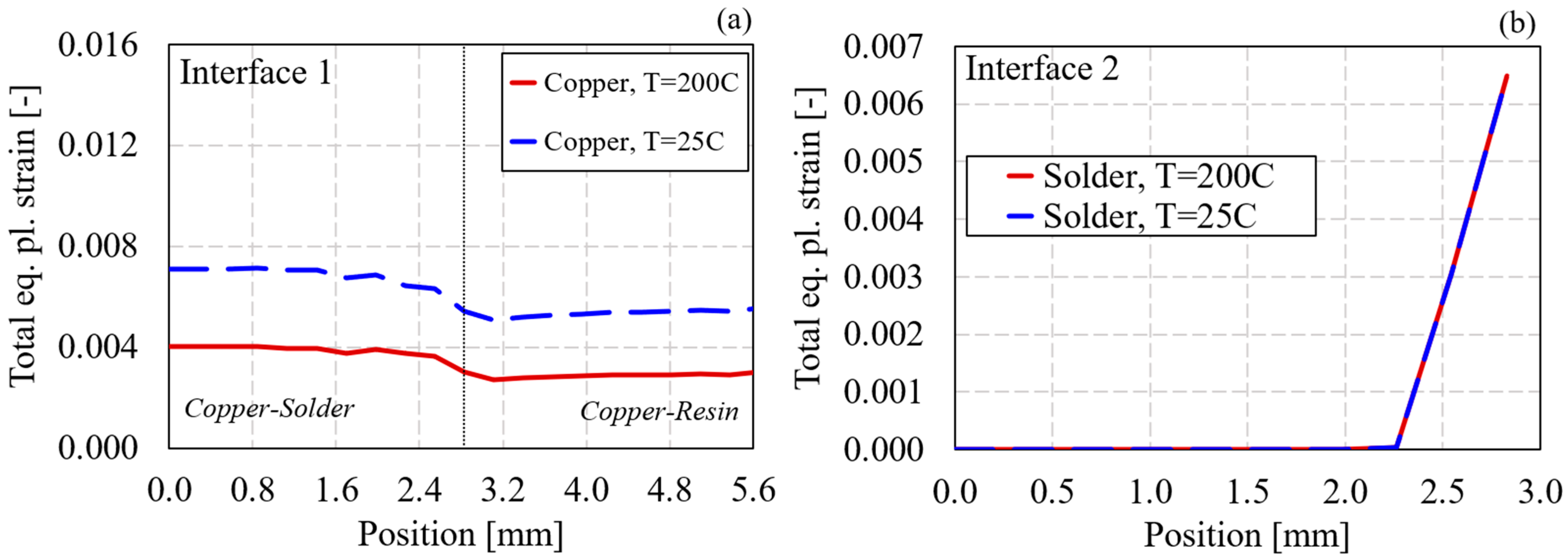
As previously mentioned, the molding process also results in the accumulation of plastic deformation in the material layers where plasticity is considered. Figure 11 shows the accumulated plastic deformation at 200 and 25 °C at Interface 1 (copper–solder), Interface 2 (solder-SiC). In particular, in Figure 11a, the equivalent accumulated plastic strain is considered in the nodes belonging to copper. The equivalent plastic strain accumulated at the solder nodes was negligible.
During cooling, the copper accumulates plastic strain. On the other hand, no plastic deformation occurs in the polyimide, irrespective of the considered interface.
At the end of the manufacturing process, the plastic strain of the copper glued below the solder presents a horizonal plateau at about 0.007 (0.7%). A comparable value of plastic strain is found at the top surface of the solder (Interface 2). Here the maximum plastic strain is about 0.065 (0.65%). The difference in plastic deformation between the lower side (Interface 1) and the upper side (Interface 2) in the solder can be related to the different thermal expansion between copper, solder, and SiC. Indeed, the coefficient of thermal expansion of the solder is 1.65 times higher than that of the copper, while it is 7.25 times higher than that of the SiC. The remarkable difference in terms of thermal expansion at Interface 2 results in the accumulation of more plastic deformation.
The numerical evidence of residual plastic deformation in power electronic packages induced by the production process is a new finding to the author’s knowledge. Indeed, very often, when numerical simulations aiming at assessing the life performance and reliability of power electronic components are performed, the initial state of the material after manufacturing is either neglected or is just approximately simulated by way of the “stress-free temperature” concept, which may eventually deliver the overall warpage of the power module but cannot accurately predict the spatial distributions of stresses and strains.
However, the numerical results reported here clearly show that the thermomechanical interactions between the different material layers during the solidification process play an important role in the onset of residual stress as well as residual plastic deformation. It must be noticed that, even if the reported values of plastic strain can appear small to the reader, they can dramatically affect the overall life performance of the package. Indeed, together with the stress state discussed in the previous section, the plastic deformation represents a key parameter lying at the origin of the possible onset of failure phenomena such as the loss of adhesion and consequent delamination [9,39,40].

4.3. Insights into the Resin Permanent Straining Before Solidification

The equivalent plastic strain accumulated by the resin at the interfaces with the SiC, polyimide, and copper along the x direction is given in Figure 12. Particularly, the distribution of total equivalent plastic strain before zeroing of plastic strain (T = 49 °C) along the reference path is shown in Figure 12a. Before zeroing of plastic strain (Sim. 1), the maximum plastic strain of about 0.1% is found at the external corner of the resin–polyimide interface (indicated with the point A in Figure 12). It is worth mentioning that the accumulated plastic strain does not have any specific physical meaning during Sim. 1. Indeed, before curing, the resin still behaves as a viscous material. On the other hand, the accumulation of plastic deformation is a direct consequence of the modeling choice. Figure 12b shows that, thanks to its purely plastic response with negligible yield stress, the resin in Sim. 1 complies with the displacements of the deforming assembly by cumulating plastic strains at very low yield together with negligible elastic strains, then opposing negligible resistance (developing no internal stresses). At the end of the Sim. 1, as the resin starts curing at 50 °C, the cumulated plastic strains are zeroed, while the elastic ones are already negligible thanks to the very low yield stress. This ensures that no unrealistic stresses are going to be developed in the next simulation phases, when the resin solidification causes the elastic modulus to increase. Therefore, Sim. 1 approximates the mechanical response of the actual resin in its state of a heated, slightly viscous fluid, sticking onto the assembly and moving together with its expansion. The zeroing of plastic strains at 50 °C (end of Sim. 1) sets the current configuration of the resin alone as its stress-free configuration, ready to start solidifying, as it really occurs in the physical phenomena. In the successive phases, Sim. 2 and Sim. 3. The resin is purely elastic, with, respectively, temperature-dependent modulus (Sim. 2) and constant modulus (Sim. 3); therefore, no plastic strain is accumulated anymore, again reflecting the physics of the real molding phenomena.

4.4. Warpage

Reliability studies on power electronic components usually include the assessment of the package warpage, namely, the out-of-plane displacement of the component, under different thermomechanical gradients reproducing the working conditions. The ideal condition of zero warpage corresponds to perfectly flat package, meaning that all components do not present any shape variations after the application of the thermomechanical cycles, either due to the technological processes for their production, to the passive cycles imposed for their qualification, or to the active cycling of their operational life. However, experimental work and numerical simulations [10,11,12] put into evidence that thermomechanical loads in all the above conditions often result in the component warpage. This phenomenon must be mitigated since it can result in imperfect connection between different layers during the package assembling or in the degradation and anticipated failure of the electrical and thermal performance of the component during its operational life. The warpage of the targeted component is discussed here, analyzing the out-of-plane displacement at the top side of the resin at the peak temperature of 200 °C as well as at 25 °C after the resin molding procedure is completed. Figure 13 shows that the solidification process can result in a remarkable warpage at the top surface of the resin capsule.
At 200 °C, the greatest positive out-of-plane displacement is found at the center of the component (“crying” shape of the assembly). This configuration is maintained after the cooling phase down to 25 °C although warpage values are lower.
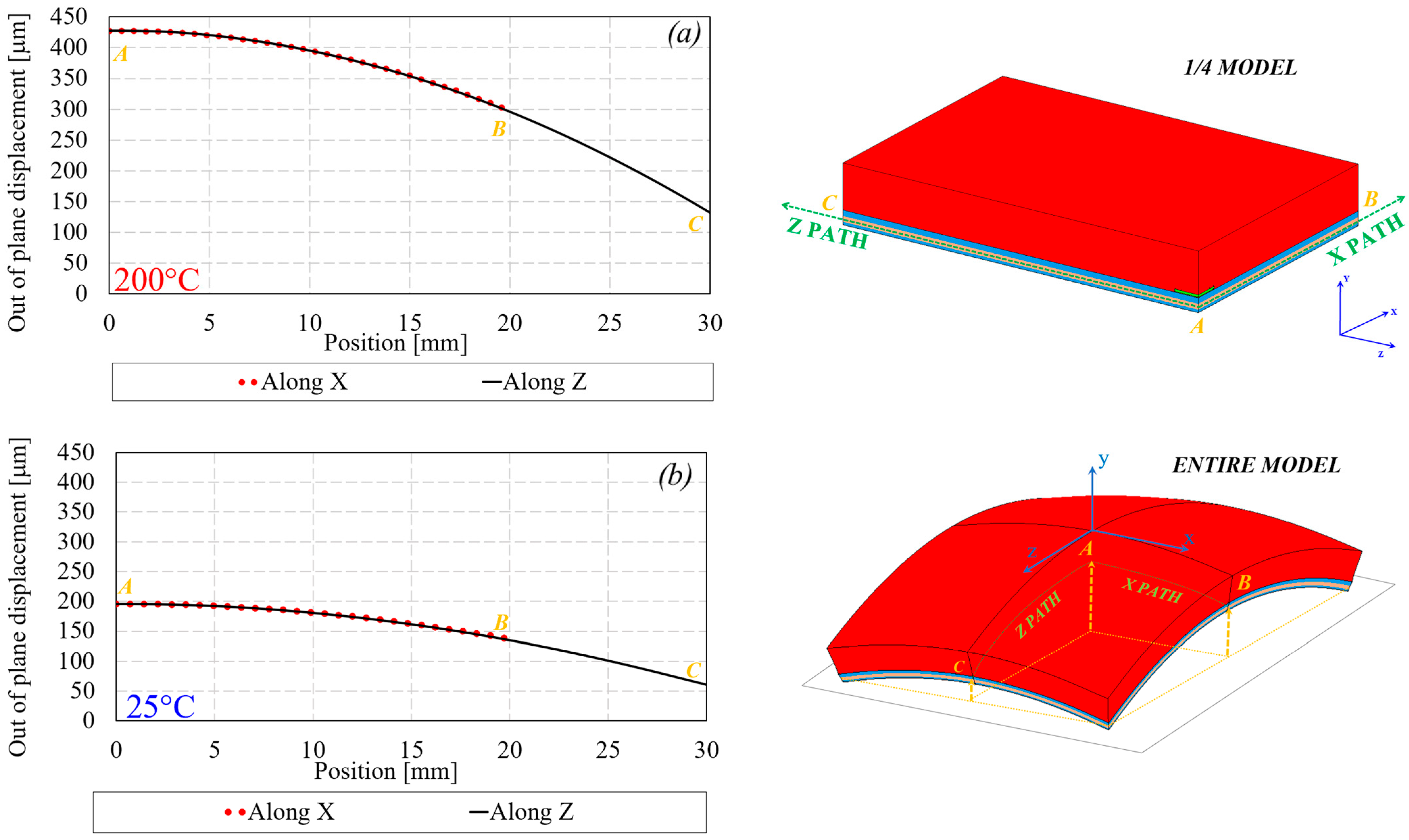
The warpage of the device is further discussed by analyzing the distributions of out-plane displacement along two paths, respectively, parallel to the x-axis and the z-axis, both passing by the center of the assembly plan view, at the mid-plane level of the AMB (see Figure 14). Interestingly, at both 200 °C and at 25 °C, the out-of-plane displacement along both paths follows the same trend, suggesting an almost symmetrical deformation. This result further indicates a cry-type shape after the manufacturing step of resin molding, provided that in this work the AMB is assumed to be flat at the beginning of the resin molding.
The above simulations put into evidence that the shape variation induced by the manufacturing cannot be neglected and that the initial state of the material after the production process must be taken into account. This finding highlights that the assumption of undeformed assembly as a reference starting configuration in the reliability assessment of power modules [11,12,13] is approximated.
Similar analyses carried out in sequences for the multiple steps of the manufacturing process (e.g., taking into account the pre-warpage of the AMB due to its own production issues) might then lead to accurate predictions of the real final shape of the whole power electronic package and of its internal pre-stresses.
The warpage predictions provided in Figure 13 and Figure 14 refer to a representative commercial SiC-based power module for automotive applications, with no direct correspondence to any actual device. Therefore, a compatibility check for such predictions is provided here by comparing them against experimental data from literature for similar devices, as shown below.
The proposed modeling approach delivers a “crying” warpage of approximately 430 µm at the end of the heating phase (T = 200 °C) and a smaller crying warpage around 200 µm (Figure 13) at the end of the curing cycle (T = 25 °C). Therefore, the cooling phase caused a “relative-smiling” warpage of around 230 µm.
Forndran et al. [19] provided the experimental warpage of a commercial power module with composition and geometry comparable to those of the present work (AMB substrate with die and encapsulating resin, size roughly 60 × 50 mm). Those authors referred to a resin-curing thermal cycle (25–175–25 °C). At 175 °C, i.e., after the heating phase, the package is considered stress-free and flat. Then, at 25 °C, after both the heating and cooling phases, a smiling warpage of 200 µm is reported from experiments and simulations.
Consequently the present work agrees with the results from [19] in predicting that the cooling stage in the resin molding process (respectively, from 200 to 25 °C and from 175 to 25 °C) induces a warpage close to 200 µm in the smiling verse (e.g., smiling if starting from a flat shape, reducing the crying magnitude if starting from pronounced crying shape).
The residual stresses arising from the production process are expected to affect the durability of power electronics by interacting with the mechanical response to the operating thermomechanical loads, including nonlinear phenomena like plastic straining and time-dependent phenomena such as creep [41], mostly affecting the solder. Then, the damage-delamination models for correctly predicting the structural integrity of power electronics should take into account such interactions. Therefore, the evaluation of residual stresses and permanent strains proposed here for the resin molding is a preliminary step for the future development of modeling procedures aimed at simulating such interactions.

5. Conclusions

This study presents an advanced FE modeling approach to evaluate the mechanical response of SiC-based multilaminar semi-finished assemblies, as part of power electronic packages commonly used in electric vehicles, subjected to the influence of a representative step of their manufacturing process.
The novelty of the present work lies in the innovative approach to model the phase changes in the resin molding, describing the progressive stiffening of the resin while its adhesion to the package takes place, including the elastoplastic nonlinear behavior of materials (commonly neglected in the literature) and an accurate simulation of the mechanical interaction between the encapsulant resin and the underlying layers during the resin curing process.
The warpage predicted by this modeling approach proved to be compatible with experimental results from literature. Moreover, the modeling strategy (post-yield response, layer contact, mesh sensitivity) was already validated in a previous work with less sensitive available experimental data from similar packages.
The resin molding process was simulated by analyzing the mechanical response of the whole assembly, accounting for resin solidification through varying its plastic and elastic properties and its adhesion to the mating surfaces of the package.
The transition from fluid to solid and the change in resin stiffness occurring while the adhesion to the package takes place were shown to generate significant internal stresses, plastic strains, and to induce the final deformed shape of the power electronics assembly. Residual stresses at material interfaces reveal that manufacturing directly triggers a preload field, potentially accelerating mechanical failures and performance degradation under operational thermomechanical loads. Then, resin molding influences the final shape and quality of the module, as surface non-planarity can severely undermine subsequent production, installation, and connection steps in assembling complex power electronics modules. Therefore, this study confirmed that assuming a stress-free state in the as-received package can be inaccurate and that also the improved ‘stress-free temperature approach’ is insufficient to capture the details and phenomena addressed by the proposed simulation strategy.
The computational cost of this procedure is as low as that of common elastoplastic analyses simulating sequences of two or three loading conditions. For a finite element model with around 65,000 elements and nonlinear, finite-plasticity analyses of 180 steps, the duration of a complete run on a current consumer laptop is around 1 h.
The procedure proposed here could be of practical application in industry for the design of power electronics in order to predict the warpage and the residual stresses within the package at the end of the production process. This would deliver an effective non-zero stress starting condition at room temperature of the just-produced package, to which we superimpose the operating thermomechanical loads for achieving the effective stress–strain conditions such packages undergo during their life.
Resin molding is considered here as it causes large changes in the mechanical stiffness of the package with respect to other technological production steps such as soldering, passivation, etc. However, the rationale of the proposed procedure can also be adopted for predicting the deformations and residual stresses from other production steps involving the transition from two or more independent fluid or solid layers to mechanically coupled solid bodies under variable temperatures. Given such a general character of the proposed approach, the package size-shape, the material properties, and the temperature histories adopted can be considered to be representative of a class of products and production processes.

Author Contributions

Conceptualization, G.M.; methodology, R.B.; validation, G.B.; formal analysis, G.B.; investigation, L.C. and R.B.; data curation, L.C. and G.B.; writing—original draft preparation, L.C.; writing—review and editing, G.M., R.B. and G.B.; visualization, L.C.; supervision, G.M.; project administration, G.M.; funding acquisition, G.M. All authors have read and agreed to the published version of the manuscript.

Funding

This work has been partially funded by European Union (NextGeneration EU), through the MUR-PNRR project SAMOTHRACE (ECS00000022).

Data Availability Statement

The raw data supporting the conclusions of this article will be made available by the authors on request.

Conflicts of Interest

The authors declare no conflicts of interest.

References

  1. Perreault, D.J.; Afridi, K.K.; Khan, I.A. 32—Automotive Applications of Power Electronics. In Power Electronics Handbook, 4th ed.; Rashid, M.H., Ed.; Butterworth-Heinemann: Oxford, UK, 2018; pp. 1067–1090. ISBN 978-0-12-811407-0. [Google Scholar]
  2. Liu, G.; Wu, Y.; Li, K.; Wang, Y.; Li, C. Development of High Power SiC Devices for Rail Traction Power Systems. J. Cryst. Growth 2019, 507, 442–452. [Google Scholar] [CrossRef]
  3. Lee, H.; Smet, V.; Tummala, R. A Review of SiC Power Module Packaging Technologies: Challenges, Advances, and Emerging Issues. IEEE J. Emerg. Sel. Top. Power Electron. 2020, 8, 239–255. [Google Scholar] [CrossRef]
  4. Yang, Y.; Dorn-Gomba, L.; Rodriguez, R.; Mak, C.; Emadi, A. Automotive Power Module Packaging: Current Status and Future Trends. IEEE Access 2020, 8, 160126–160144. [Google Scholar] [CrossRef]
  5. Muscato, O.; Di Stefano, V. An Energy Transport Model Describing Heat Generation and Conduction in Silicon Semiconductors. J. Stat. Phys. 2011, 144, 171–197. [Google Scholar] [CrossRef]
  6. Mirone, G.; Sitta, A.; D’Arrigo, G.; Calabretta, M. Material Characterization and Warpage Modeling for Power Devices Active Metal Brazed Substrates. IEEE Trans. Device Mater. Relib. 2019, 19, 537–542. [Google Scholar] [CrossRef]
  7. Zhu, N.; Lee, S.Y.; van Wyk, J.D.; Odendaal, W.G.; Liang, Z.X. Thermal Stress and Intrinsic Residual Stress in Embedded Power Modules. In Proceedings of the 38th IAS Annual Meeting on Conference Record of the Industry Applications Conference, Salt Lake City, UT, USA, 12–16 October 2003; Volume 2, pp. 1244–1250. [Google Scholar]
  8. Liu, S.; Yan, Y.; Zhou, Y.; Han, B.; Wang, B.; Zhang, D.; Xue, S.; Wang, Z.; Yu, K.; Shi, Y.; et al. Thermal Induced Interface Mechanical Response Analysis of SMT Lead-Free Solder Joint and Its Adaptive Optimization. Micromachines 2022, 13, 908. [Google Scholar] [CrossRef]
  9. Dudek, R.; Doering, R.; Pufall, R.; Kanert, W.; Seiler, B.; Rzepka, S.; Michel, B. Delamination Modeling for Power Packages by the Cohesive Zone Approach. In Proceedings of the 13th InterSociety Conference on Thermal and Thermomechanical Phenomena in Electronic Systems, San Diego, CA, USA, 30 May–1 June 2012; IEEE: San Diego, CA, USA, 2012; pp. 187–193. [Google Scholar]
  10. Strydom, J.T.; van Wyk, J.D. Investigation of Thermally Induced Failure Mechanisms in Integrated Spiral Planar Power Passives. In Proceedings of the Conference Record of the 2002 IEEE Industry Applications Conference. 37th IAS Annual Meeting (Cat. No.02CH37344), Pittsburgh, PA, USA, 13–18 October 2002; Volume 3, pp. 1781–1786. [Google Scholar]
  11. Zhu, N.; Van Wyk, J.D.; Liang, Z.X. Thermal-Mechanical Stress Analysis in Embedded Power Modules. In Proceedings of the 2004 IEEE 35th Annual Power Electronics Specialists Conference, Aachen, Germany, 20–25 June 2004; Volume 6, pp. 4503–4508. [Google Scholar]
  12. Ye, H.; Lin, M.; Basaran, C. Failure Modes and FEM Analysis of Power Electronic Packaging. Finite Elem. Anal. Des. 2002, 38, 601–612. [Google Scholar] [CrossRef]
  13. Sitta, A.; Renna, M.; Messina, A.A.; Mirone, G.; D’Arrigo, G.; Calabretta, M. Power Module Ceramic Substrates: Mechanical Characterization and Modeling. In Proceedings of the 2020 21st International Conference on Thermal, Mechanical and Multi-Physics Simulation and Experiments in Microelectronics and Microsystems (EuroSimE), Cracow, Poland, 5–8 July 2020; IEEE: Cracow, Poland, 2020; pp. 1–5. [Google Scholar]
  14. Struzziero, G.; Nardi, D.; Sinke, J.; Teuwen, J.J.E. Cure-Induced Residual Stresses for Warpage Reduction in Thermoset Laminates. J. Compos. Mater. 2020, 54, 3055–3065. [Google Scholar] [CrossRef]
  15. Gschwandl, M.; Fuchs, P.F.; Mitev, I.; Yalagach, M.; Antretter, T.; Qi, T.; Schingale, A. Modeling of Manufacturing Induced Residual Stresses of Viscoelastic Epoxy Mold Compound Encapsulations. In Proceedings of the 2017 IEEE 19th Electronics Packaging Technology Conference (EPTC), Singapore, 6–9 December 2017; IEEE: Singapore, 2017; pp. 1–8. [Google Scholar]
  16. Nielsen, M.W.; Hattel, J.; Andersen, T.; Branner, K.; Nielsen, P.H. Experimental Determination and Numerical Modelling of Process Induced Strains and Residual Stresses in Thick Glass/Epoxy Laminate. ECCM 2012—Composites at Venice, Proceedings of the 15th European Conference on Composite Materials 2012. Available online: https://www.scopus.com/pages/publications/84904016051?origin=resultslist (accessed on 4 October 2025).
  17. Bogetti, T.A.; Gillespie, J.W., Jr. Process-Induced Stress and Deformation in Thick-Section Thermoset Composite Laminates. J. Compos. Mater. 1992, 26, 626–660. [Google Scholar] [CrossRef]
  18. Mirone, G.; Barbagallo, R.; Bua, G.; La Rosa, G. Finite Element Simulation and Sensitivity Analysis of the Cohesive Parameters for Delamination Modeling in Power Electronics Packages. Materials 2023, 16, 4808. [Google Scholar] [CrossRef] [PubMed]
  19. Forndran, F.; Sprenger, M.; Barrera, J.R.; Steinau, M.; Roellig, M.; Muench, S. Modelling Warpage Behavior of Molded Power Modules for Electric Vehicles. In Proceedings of the 2024 25th International Conference on Thermal, Mechanical and Multi-Physics Simulation and Experiments in Microelectronics and Microsystems (EuroSimE), Catania, Italy, 7–10 April 2024; IEEE: Catania, Italy, 2024; pp. 1–6. [Google Scholar]
  20. Mirone, G.; Barbagallo, R.; Bua, G.; Sitta, A.; Calabretta, M.; Sequenzia, G. Thermal-Structural Modeling of Power Electronic Package: Effects of Deposition Geometry and Dry Spot on the Stress Distributions. IOP Conf. Ser. Mater. Sci. Eng. 2024, 1306, 012012. [Google Scholar] [CrossRef]
  21. Schuderer, J.; Liu, C.; Pavlicek, N.; Salvatore, G.; Loisy, J.-Y.; Schroeder, A.; Torresin, D.; Gradinger, T.; Baumann, D.; Mohn, F.; et al. High-Power SiC and Si Module Platform for Automotive Traction Inverter. In Proceedings of the PCIM Europe 2019; International Exhibition and Conference for Power Electronics, Intelligent Motion, Renewable Energy and Energy Management, Nuremberg, Germany, 7–9 May 2019; pp. 1–8. [Google Scholar]
  22. Available online: https://www.st.com/en/power-transistors/stpower-n-channel-mosfets-gt-200-v-to-700-v/documentation.html (accessed on 1 October 2025).
  23. O’Neill, A.; Vavasour, O.J.; Russell, S.; Arith, F.; Urresti, J.; Gammon, P.M. Dielectrics in Silicon Carbide Devices: Technology and Application. Adv. Silicon Carbide Electron. Technol. II 2020, 69, 63–106. [Google Scholar]
  24. Mirone, G.; Barbagallo, R.; Corallo, L.; Bua, G.; La Rosa, G.; Fargione, G.; Giudice, F. Nonlinear Elastoplastic Response and Damage Modeling in Power Electronics Packages Under Thermal Cycling. Eng. Proc. 2025, 85, 50. [Google Scholar]
  25. Sun, Y.; Lee, H.-S.; Han, B. Measurement of Elastic Properties of Epoxy Molding Compound by Single Cylindrical Configuration with Embedded Fiber Bragg Grating Sensor. Exp. Mech. 2017, 57, 313–324. [Google Scholar] [CrossRef]
  26. Zhao, J.-H.; Ryan, T.; Ho, P.S.; McKerrow, A.J.; Shih, W.-Y. Measurement of Elastic Modulus, Poisson Ratio, and Coefficient of Thermal Expansion of on-Wafer Submicron Films. J. Appl. Phys. 1999, 85, 6421–6424. [Google Scholar] [CrossRef]
  27. MatWeb: Overview of the Properties of Epoxy Molding Compound. Available online: https://www.Matweb.Com/Search/DataSheet.Aspx?MatGUID=d32b84b0ef1e410596e9dda9e02429c7&ckck=1 (accessed on 1 October 2025).
  28. MatWeb: Overview of the Mechanical Properties of SiC. Available online: https://www.Matweb.Com/Search/QuickText.Aspx?SearchText=SiC (accessed on 1 October 2025).
  29. MatWeb: Overview of the Properties of Eutectic Solder (63Sn-37Pb)—ASTM B 32 Grade Sn63. Available online: https://www.Matweb.Com/Search/Datasheet.Aspx?Matguid=3a5c8bc670914d588b26ab0b994d88cb&ckck=1 (accessed on 1 October 2025).
  30. MatWeb: Overview of the Mechanical Properties of Si3N4. Available online: https://www.Matweb.Com/Search/QuickText.Aspx?SearchText=Si3N4 (accessed on 1 October 2025).
  31. Agag, T.; Koga, T.; Takeichi, T. Studies on Thermal and Mechanical Properties of Polyimide–Clay Nanocomposites. Polymer 2001, 42, 3399–3408. [Google Scholar] [CrossRef]
  32. Kabaar, A.B.; Buttay, C.; Dezellus, O.; Estevez, R.; Gravouil, A.; Gremillard, L. Characterization of Materials and Their Interfaces in a Direct Bonded Copper Substrate for Power Electronics Applications. Microelectron. Reliab. 2017, 79, 288–296. [Google Scholar] [CrossRef]
  33. He, J.; Ling, Y.; Lei, D. Mechanical Properties of Sn–Pb Based Solder Joints and Fatigue Life Prediction of PBGA Package Structure. Ceram. Int. 2023, 49, 27445–27456. [Google Scholar] [CrossRef]
  34. Munro, R.G. Material Properties of a Sintered α-SiC. J. Phys. Chem. Ref. Data 1997, 26, 1195–1203. [Google Scholar] [CrossRef]
  35. Hoffmann, M.J.; Petzow, G.; NATO (Eds.) Tailoring of Mechanical Properties of Si3N4 Ceramics; NATO ASI series Series E, Applied sciences; Kluwer Academic: Dordrecht, The Netherlands; London, UK, 1994; ISBN 978-0-7923-3119-3. [Google Scholar]
  36. Matsui, M.; Masuda, M. Fracture Behavior of Silicon Nitride at Elevated Temperatures. In Tailoring of Mechanical Properties of Si3N4 Ceramics; Hoffmann, M.J., Petzow, G., Eds.; Springer: Dordrecht, The Netherlands, 1994; pp. 403–414. ISBN 978-94-011-0992-5. [Google Scholar]
  37. Ucar, Y.; Akova, T.; Aysan, I. Mechanical Properties of Polyamide Versus Different PMMA Denture Base Materials. J. Prosthodont. 2012, 21, 173–176. [Google Scholar] [CrossRef]
  38. Bouzakis, K.-D.; Tsiafis, I.; Michailidis, N.; Tsouknidas, A. Determination of Epoxy Resins’ Mechanical Properties by Experimental-Computational Procedures in Tension. J. Balk. Tribol. Assoc. 2009, 15, 18–24. Available online: https://www.scopus.com/pages/publications/64649099668?origin=resultslist# (accessed on 4 October 2025).
  39. Adler, C.; Morais, P.; Akhavan-Safar, A.; Carbas, R.J.C.; Marques, E.A.S.; Karunamurthy, B.; Da Silva, L.F.M. Cohesive Properties of Bimaterial Interfaces in Semiconductors: Experimental Study and Numerical Simulation Using an Inverse Cohesive Contact Approach. Materials 2024, 17, 289. [Google Scholar] [CrossRef] [PubMed]
  40. Calabretta, M.; Sitta, A.; Oliveri, S.M.; Sequenzia, G. Copper to Resin Adhesion Characterization for Power Electronics Application: Fracture Toughness and Cohesive Zone Analysis. Eng. Fract. Mech. 2022, 266, 108339. [Google Scholar] [CrossRef]
  41. Zhao, S.; Yang, X.; Wu, X.; Liu, G. Investigation on Creep-Fatigue Interaction Failure of Die-Attach Solder Layers in IGBTs Under Power Cycling. IEEE Trans. Power Electron. 2025, 40, 7261–7274. [Google Scholar] [CrossRef]
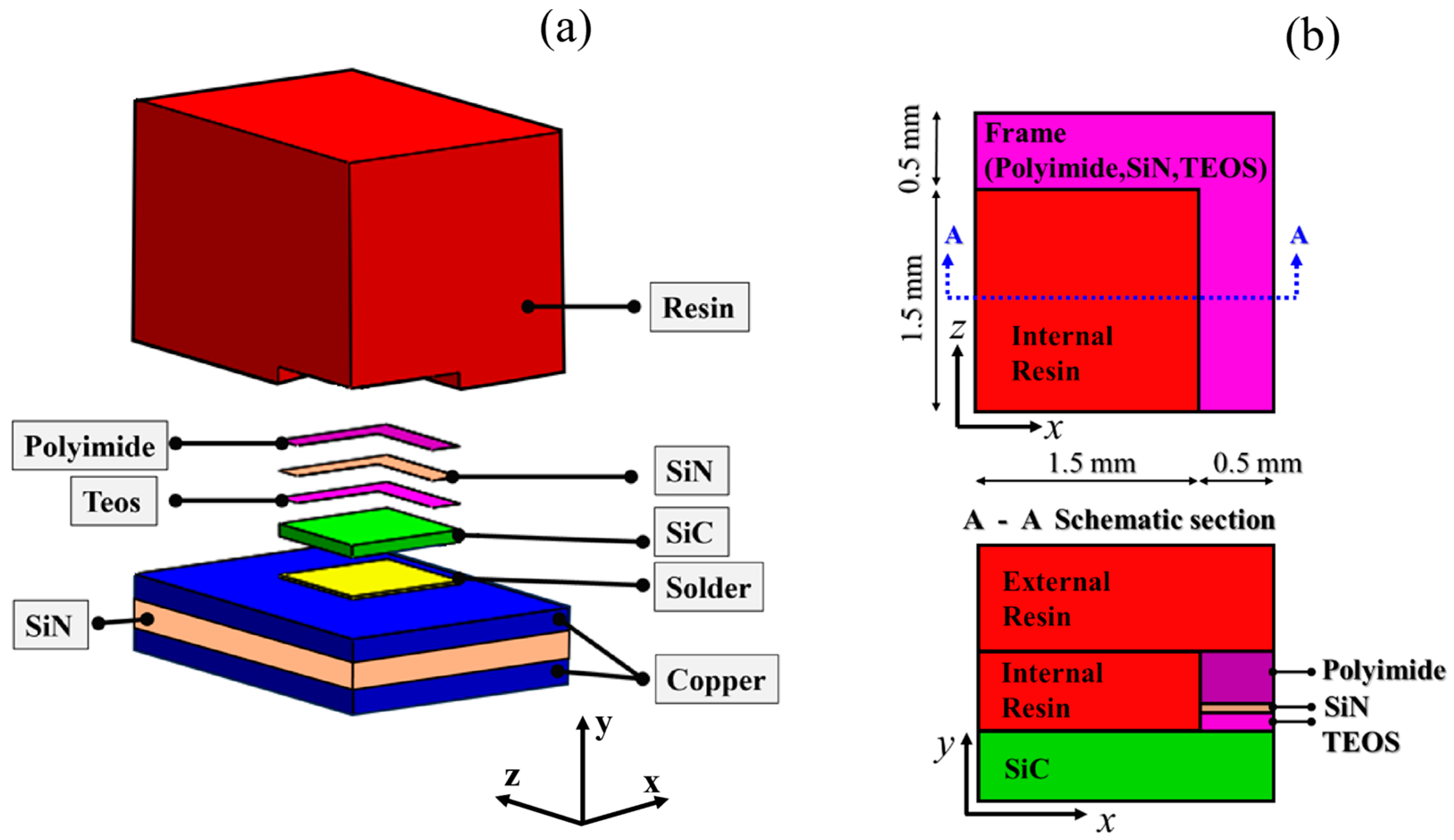
Figure 1. (a) Exploded isometric view of the central zone of the model; (b) detailed views of the multilaminae assembly incorporating SiC, TEOS, SiN, polyimide, and resin. Only a quarter of the assembly is considered thanks to the symmetries.
Energies 18 05364 g001
Figure 2. Thermal gradient reproducing the molding cycle. Curing starts at 50 °C and ends at 150 °C.
Energies 18 05364 g002
Figure 3. Mesh adopted to discretize the electronic assembly.
Energies 18 05364 g003
Figure 4. Flow curves solder [29], polyimide [31] and copper [32].
Energies 18 05364 g004
Figure 6. (a) Schematic representations of paths (lengths in mm) considered for the two interfaces and (b) representation of normal and shear stress tensor components: blue arrows indicate the stress components shared by two neighboring layers, while the black ones indicate the stress components acting just below the interface and, thus, acting on a specific material.
Energies 18 05364 g006
Figure 7. Stress distributions at all interfaces along the paths given in Figure 6 at the peak temperature, T = 200 °C.
Energies 18 05364 g007
Figure 8. Minimum, average and maximum stresses along all considered interfaces at the peak temperature, T = 200 °C.
Energies 18 05364 g008
Figure 9. Stress distributions at all interfaces along the paths given in Figure 6 at the end of cooling, T = 25 °C.
Energies 18 05364 g009
Figure 10. Minimum, average and maximum stresses along all considered interfaces at the end of cooling, T = 25 °C.
Energies 18 05364 g010
Figure 11. Plastic strain distributions plotted at the end of heating and cooling phase, extracted at two interfaces: Interface 1 Copper-Solder (a); Interface 2 solder-SiC (b).
Energies 18 05364 g011
Figure 12. (a) Total equivalent plastic strain along x at the interfaces resin–SiC, resin–polyimide, and resin–copper before zeroing of plastic strain (T = 49 °C). (b) History plot of total equivalent plastic strain, total elastic strain, and Mises stress at the resin location (A) of maximum plastic deformation before zeroing of the plastic strain. (c) Scheme of the assembly and identification of the analyzed resin location.
Energies 18 05364 g012
Figure 13. Contour plots out-of-plane displacement Uy at the (a) peak temperature and (b) at the end of the cooling stage at the top surface of the resin (orange plane in (c)).
Energies 18 05364 g013
Figure 14. Path plots of the out-of-plane displacement at the middle section of the AMB along the x-axis (a) and z-axis (b).
Energies 18 05364 g014
Table 1. Summary of dimensions of the layers constituting the assembly, denomination of element formulation in Hexagon Marc 2023.4 software, and number of elements per layer. Note that SE and SSE are used to indicate solid elements and solid shell elements, respectively.
AMB Copper Bottom AMB SiNAMB Copper TopSolderSiCTEOSSiNPoly.Internal
Resin
External
Resin
Length along x [mm]202020222221.55
Length along z [mm]303030222221.57.5
Thickness [mm]0.240.480.480.50.22 × 10−31 × 10−36 × 10−39 × 10−95
Element
type [-]
SE
HEX-8
SE
HEX-8
SE
HEX-8
SSE
HEX-8
SE
HEX-8
SSE
HEX-8
SSE
HEX-8
SSE
HEX-8
SSE
HEX-8
SEE
HEX-8
N. Elements [-]811216,22416,224400500200200200488628
Avg. Element size (x,z,y) [mm3]0.5 × 0.2 × 0.12 0.5 × 0.2 × 0.12 0.5 × 0.2 × 0.12 0.2 × 0.2 × 0.01250.2 × 0.2 × 0.040.05 × 0.15 × 0.0020.05 × 0.15 × 0.0010.05 × 0.15 × 0.0060.2 × 0.25 × 0.0090.2 × 0.25 × 0.24
Disclaimer/Publisher’s Note: The statements, opinions and data contained in all publications are solely those of the individual author(s) and contributor(s) and not of MDPI and/or the editor(s). MDPI and/or the editor(s) disclaim responsibility for any injury to people or property resulting from any ideas, methods, instructions or products referred to in the content.