Abstract
Basin insulator is a critical component of gas-insulated transmission line (GIL) systems. Air gap defects and surface crack defects may form in basin insulators due to casting, installation, or transport processes. This phenomenon poses a significant threat to long-term safety and stability and may even lead to partial discharges. This study establishes a simulation model of a GIL system-incorporating insulator to systematically analyze the influence patterns of various defects on the insulation characteristics of the basin insulator. Meanwhile, an equation predicting the relationship between defect size and maximum electric field strength is derived. The research revealed the following: For short air gap defects near the conductor, increasing length reduces their impact on the surrounding electric field, with the radius having minimal effect; for long air gap defects near the conductor, increasing length amplifies their influence. Smooth air gap defects distant from the conductor show negligible variation in maximum electric field strength with increasing length, while unsmooth air gap defects exhibit more pronounced effects at shorter lengths. Under identical conditions, unsmooth air gap defects demonstrate greater influence on the electric field than smooth ones. For elliptical surface defects, variations in radius show the strongest distortion. The degree of influence from surface crack defects correlates directly with their proximity to the conductor. These findings provide critical diagnostic criteria for assessing the insulation performance of basin insulator under damaged conditions.
1. Introduction
Gas-insulated transmission lines (GIL) have gained widespread application due to their advantageous properties, including their compact footprint, flexible installation, high reliability and long service life [1,2,3]. Basin insulators fulfil a pivotal function within GIL systems, providing support to conductors and facilitating electrical insulation. Nevertheless, sustaining elevated standards of safety and stability in basin insulator is becoming progressively challenging.
As a result of the casting process, the installation process and the transport process, air gaps may form within the insulator. In addition, cracks may appear on the surface of the insulator [4,5]. This phenomenon poses a considerable threat to long-term safety and stability, and may result in critical faults, including gas leakage or partial discharges [6,7]. It has been demonstrated that defective basin insulator is susceptible to insulation failures [8]. Consequently, the analysis of the distribution of electric fields in basin insulator under varying damage conditions is of paramount importance for the optimization of their design.
In the research concerning the influence of defects in basin insulators on electric field distribution and insulation performance, a large number of scholars have carried out targeted studies. In [9], Wang HaoRan et al. investigated the effects of typical defects (such as air gaps on the conductor surface, protrusions and depressions on the basin surface) on the electric field distribution of ultra high voltage basin insulator. In [10], a defect model of metallic foreign objects adhering to the surface of basin insulator was designed by Wang HongMei et al., and the triggers of sudden breakdown or flashover of solid insulation were analyzed. In [11], Cang Wenzhi et al. investigated the electric field deformation of insulators under different defect conditions of air gap defects that are shaped as long cylinders and examined the manifestation of electric field distortion caused by different defect conditions. In [12], He Baina et al. modeled the impact of bubble size and location within the basin insulator on electric field distribution and flashover along its surface, and the results revealed that internal defects in basin insulators cause severe electric field distortion. In [13], Ueta G et al. investigated the effects of three types of microscopic defects—delamination, cracks and internal voids—on the insulating performance of basin insulator. In [14], an experimental platform targeting surface discharge defects in 220 kV GIS was established by Qi Bo et al. The study investigated the characteristics of surface discharge phenomena in relation to the presence of fixed metal particles on insulator surfaces. In [15], Zhou Qian et al. conducted physical experimentations on archetypal insulation defects, incorporating metal particles and air gaps. This approach resulted in the acquisition of a substantial corpus of ultra-high-frequency partial discharge signal data. In [16], Ding DengWei et al. designed five varieties of defect models to simulate defects that may occur during GIS operation. Through a series of experiments, they extracted nine physically meaningful feature parameters from ultra-high-frequency signals. These were used to describe the typical characteristics of the five discharge types. In [17,18], Zuo ZhouYao et al. proposed a longitudinal wave propagation technique to assess the internal stress condition of basin insulator, thereby enabling the detection of cracks in basin insulator. In [19], Chen Chen et al., based on the ultrasonic intelligent diagnosis method, detected the internal defects of the basin insulator.
Currently, most research on basin insulators mainly focuses on the electric field simulation of internal air gap defects, metal wire defects and suspended particle defects, as well as conventional defect detection methods. However, there remains a lack of research on the influence laws of different defect types on the insulation performance of basin insulators when defects exist and on insulation performance prediction based on defect size, location and orientation. Taking the basin insulator used in 550 kV GIL as the research object, this study establishes an electric field simulation model of the 550 kV basin insulator and systematically explores the influence mechanisms of different types of defects on the insulation performance of the basin insulator under different location and size conditions.
2. Failure Overview
Figure 1 illustrates the physical phenomena of insulation failure that occurred during a 760 kV AC voltage withstand test on a 550 kV GIL basin insulator prior to its use in a project. The area within the red box shows flashover phenomena; additionally, the insulator surface exhibits burn marks, and visible cracks are present inside the insulator. The insulator had passed the 760 kV AC voltage test at the factory. It is possible that the basin insulator collided with the conductor during transport, resulting in damage to the insulator’s internal or external structure. The defective basin insulator with internal air gaps or surface cracks failed the 760 kV AC voltage withstand test due to the presence of high electric field strength in the defective areas, which resulted in partial discharges, leading to breakdown of the insulator during the test.
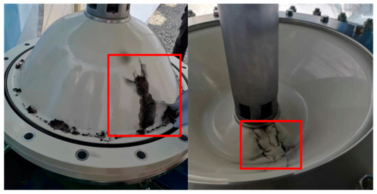
Figure 1.
Macroscopic morphology of faulty basin insulator.
This fault incident highlights the critical importance of basin insulator quality for the safe and stable operation of GIL systems. Insulation faults caused by basin insulator account for a significant proportion of total faults during GIL operation. In order to prevent similar issues from recurring, it is crucial to investigate the cause of this fault. This paper presents a simulation model of the electrical field for a 550 kV basin insulator, which is used to study the impact of different levels of damage to the insulator on the distribution of the electrical field.
3. Model Construction and Parameters
3.1. Geometric Model Construction
This study establishes a simplified three-dimensional electric field model of a basin-type insulator under various damage conditions based on a 550 kV GIL cavity structure. The insulator damage investigated includes internal air gaps, internal cracks and surface cracks. The simulation model comprises a conductor, an enclosure and a basin insulator. The cavity is filled with SF6 gas at a pressure of 0.5 MPa. Figure 2a illustrates the complete simulation configuration, while Figure 2b shows a cross-sectional view of the upper structure to enhance clarity of observation. This paper conducts extensive analyses of insulators with different defect types under electric field conditions to investigate the impact of insulator damage on dielectric performance.
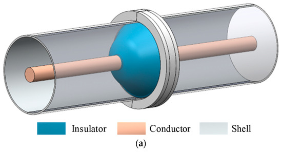
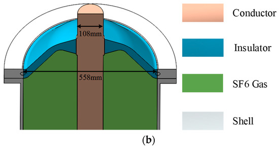
Figure 2.
(a) The 550 kV GIL structure. (b) Section of upper insulator spacer of GIL structure.
In the present study, the cavity is filled with SF6 gas (filling pressure: 0.5 MPa). The conductor and shell materials are aluminum alloys, the insulating material is epoxy resin, the medium of the air gap defects is air and the specific parameter settings are detailed in Table 1.

Table 1.
Material parameters.
3.2. FEM Mathematical Formulation
This study examines the distribution of electric fields in GIL basin insulator to determine the impact of variations in the length and position of air gaps and surface cracks across different locations. The voltage applied in the simulation is a 50 Hz industrial frequency voltage, so it can be analyzed according to the electrostatic field. Through the framework of Maxwell’s equations, the electromagnetic field problem is transformable into a computable mathematical model, adjusted to the electrostatic condition field selected as the computational model. The region of the electric field with no free charge distribution then satisfies the Laplace equation:
The relationship between electric field strength and potential is shown in Equation (2), and the boundary conditions of Equations (3) and (4) are satisfied at material interfaces between different dielectric media, with (4) not applying to interfaces where surface charges are present:
Equation (1) uses the symbol ‘ε’ to represent the dielectric constant of the medium. The relative dielectric constants at the interface of the two materials in the electric field are and . ‘’ represents the electric scalar potential. In an electric field, the potentials at the interface of the two materials are and , where E represents the magnitude of the electric field strength in the electric field in kV/mm and n represents the interface normal vector [20].
The method used in the electric field simulation is shown in Figure 3. The electrostatic module is used to calculate the electric field distribution of the basin insulator.
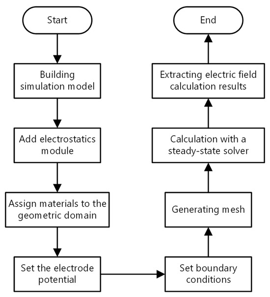
Figure 3.
Flow chart of COMSOL software.
Figure 4 shows the results of the electric field strength distribution under the defect-free condition, with the lower side showing the electric field strength distribution of the insulator section.
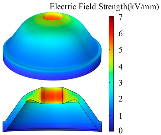
Figure 4.
FEM simulation of perfect insulation electric field strength.
For better observation, Figure 5 shows schematic diagrams of different damage conditions in the basin-type insulator. The types of defects used in basin insulators are those observed in engineering tests. Figure 5A displays short air gap defect A near the conductor with a smooth hemispherical top, Figure 5B presents long crack defect B near the conductor featuring a unsmooth air gap with tapered tip, Figure 5C illustrates elliptical surface void defect C, and Figure 5D demonstrates surface crack defect D. Smooth air gap defects have a hemispherical shape at the tip, while unsmooth air gap defects have a conical tip shape at the tip.
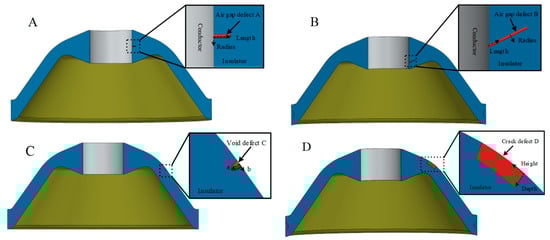
Figure 5.
(A) Schematic diagram of internal air gap defect A in basin insulator. (B) Schematic diagram of internal void defect B in basin insulator. (C) Elliptical cavity defect on insulator surface C Schematic diagram. (D) Insulator surface crack defects D Schematic diagram.
Due to the significant size difference between the air gap defect and the basin-type insulator, when performing mesh generation for a basin-type insulator model containing air gap defects, different mesh densities should be applied in different regions. A finer mesh should be used near the air gap defect, while a coarser mesh can be employed in other areas. This approach ensures both computational accuracy and a substantial reduction in calculation workload.
The mesh division is shown in Figure 6. The mesh size of the gas area is set to a maximum of 10 mm, while the grid size of the guide rods and the housing is also limited to a maximum of 10 mm. The grid size for the insulator is then limited to a maximum of 5 mm. It is imperative to note that, owing to the substantial variation in the electric field in proximity to the air gap defects, a fine grid is employed in this specific region, with a maximum grid size of 0.05 mm. The total number of grid cells is 4 million.
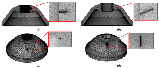
Figure 6.
(a) Air gap defect A mesh section. (b) Void defect B mesh section. (c) Elliptical surface void defect C. mesh section (d) surface crack defect D mesh section.
This study investigates the effects of various damage conditions in insulator on electric potential distribution and electric field strength, employing the finite element method (FEM) as the core analytical tool. Based on COMSOL 6.0 software, when solving, use the fully coupled solver in the stationary solver. The fully coupled solution mode solves all physical fields simultaneously, with high stability and fast convergence. A 550 kV GIL geometric model was established with material parameters defined according to Table 1, and the boundary conditions were configured in the software for electric field analysis of damaged insulator. The analysis primarily focuses on different defect types, locations and sizes.
4. Results and Analysis
4.1. Air Gap Defects A Are Located Inside the Insulator Connecting the Surface of the Conductor
In this paper, we focus on the effect of dimensional variations in the air gap defect A on the surrounding electric field strength, which ranges from 0.1 mm to 1 mm in radius and from 1 mm to 10 mm in length. The distribution of electric field strengths is shown in Figure 7a, showing that the electric field distortion is most severe at the top of the air gap defect, where the maximum electric field strength usually occurs.
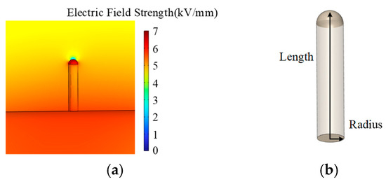
Figure 7.
(a) Electric field strength distribution around air gap defect A. (b) Geometric schematic of the air gap defect A.
The variation in maximum electric field strength with size is illustrated in the figure: when the length is 1 mm, the maximum electric field strength increases with the radius of the air gap defect; for lengths between 2 mm and 10 mm, the maximum electric field strength decreases as the radius increases. Furthermore, longer air gap defects exhibit a reduced influence on the surrounding electric field strength. Figure 7b shows the geometric schematic of the air gap defect A.
In summary, within the range of 1–10 mm in length and 0.1–1 mm in radius, the length of the air gap defect has a greater influence on the maximum electric field strength compared to its radius. The most significant impact on electric field strength occurs when the air gap defect has a length of 1 mm and a radius of 0.9 mm.
The growth in the length of the smooth air gap defects near the guide rods decreases the maximum electric field strength, which may be due to the fact that the growth in the length of the air gap defects makes the tip move away from the high field region connecting the conductor, which makes the maximum electric field strength show a decreasing trend.
To better predict the relationship between air gap defect A’s dimensions and electric field strength, this paper employs data from Figure 8 to fit the length and radius of the air gap defect against electric field strength. Air gap defects within the range of 1–10 mm in length and 0.1–1 mm in radius were fitted to the data. Within the permissible error range, the fitting equation for the length and radius of air gap defects versus electric field strength are given by Equation (5). In Equation (5), the length and radius of the air gap defect are brought into the solution, and the corresponding electric field strength E can be obtained:
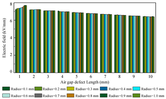
Figure 8.
The influence of air gap defect A dimensions on maximum electric field strength.
In Equation (5), E denotes the electric field strength (kV/mm), L signifies the length of the air gap defect A (mm) and R indicates the radius of the air gap defect A (mm).
4.2. Air Gap Defects B Are Located Inside the Insulator Connecting the Surface of the Conductor
Air gap defect B is a tilted air gap defect inside an insulator, which is caused by the collision of a basin insulator during transport, resulting in cracks inside the insulator, as the shape and location of the cracks produced by the collision are relatively random. In this paper, the distortion of smooth air gap defects and non-smooth air gap defects at different locations to the electric field is further investigated.
The elongated air gap defect B is designed to simulate the influence of extended crack defects within the insulator on the dielectric performance of basin-type insulator. A schematic diagram of air gap defect B is shown in Figure 9. The air gap defect B includes three configurations (B1, B2, B3): as shown in Figure 9a, B1 represents a proximal elongated air gap defect adjacent to the conductor with a smooth hemispherical tip, as shown in Figure 9b, B2 denotes a distal elongated air gap defect away from the conductor featuring smooth hemispherical structures at both ends and as shown in Figure 9a, B3 corresponds to a distal elongated air gap defect with a conical tip at the lower end and a smooth hemispherical upper end.
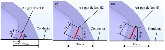
Figure 9.
(a) Schematic diagram of air gap defect B1. (b) Schematic diagram of air gap defect B2. (c) Schematic diagram of air gap defect B3.
The experiment configured three types of defects: smooth air gap defect B adjacent to the conductor; smooth air gap defects in connecting conductor B1; and air gaps with a length of 0 to 60 mm (in 10 mm increments) as well as rough air gap defect B2, also at a designated distance from the conductor. In this study, L1 is defined as the length of defect B1, L2 represents the length of smooth air gap defects B2 and L3 denotes the length of unsmooth air gap defects B3. The length ranges for both L2 and L3 are 20 mm and 40 mm.
4.2.1. Air Gap Defect B1 Within the Insulator, Contacting the Conductor Surface
The investigation was conducted with the objective of examining the impact of air gap defects in insulator on the electric field surrounding them. The subsequent analysis focused on the effect of air gaps of varying lengths on the electric field distribution when in contact with the conductor. Figure 10b shows the geometric schematic of the air gap defect B.
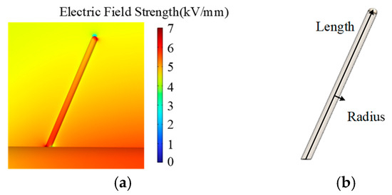
Figure 10.
(a) Electric field strength distribution around 20 mm air gap defect B1. (b) Geometric schematic of the air gap defect B.
The results show that air gap defects distort the surrounding electric field, a phenomenon that is particularly evident in the upper and lower parts of the air gap, where local intense electric field strength magnitude is observed.
Compared to the presence of air gap defects inside the insulator, the electric field strength is lowest in the absence of air gap defects inside the insulator, with a maximum electric field strength of 4.79 kV/mm. This can be derived from the data presented in Table 2. The maximum electric field strength at the air gap remains relatively constant when the length of the air gap defect attached to the conductor surface varies from 0 mm to 50 mm. The maximum electric field strengths are all in the range of 10 kV/mm. When the length of the air gap defects was 60 mm, a significant increase in the maximum electric field strength was observed. This is due to the fact that the top region of the 60 mm air gap defect is in a region of large potential gradient, resulting in a larger maximum electric field strength of the air gap defect when B1 air gap defects are present inside the basin insulator. This result suggests that an increase in the length of air gap defects leads to a relatively greater safety hazard, and that long air gaps have a greater ability to distort the surrounding electric field, which may trigger partial discharges.
Table 2.
Maximum values of electric field strength at smooth gap defects of different lengths.
4.2.2. Air Gap Defect B1 Within the Insulator
Given the random nature of the angle between the air gap defect and the conductor, this study investigates the distortion of the electric field caused by a 10 mm air gap defect at various angles. The electric field distribution when the defect-conductor angle is 40° is depicted in Figure 11. The region where the defect contacts the conductor exhibits the most severe distortion. As shown in Figure 12, where θ represents the inclination angle between the air gap defect and the conductor, ranging from 10 to 90°, with increments of 10°.
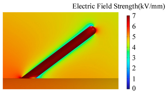
Figure 11.
Electric field distribution around 10 mm air gap defect B1 at a 40 inclination angle.
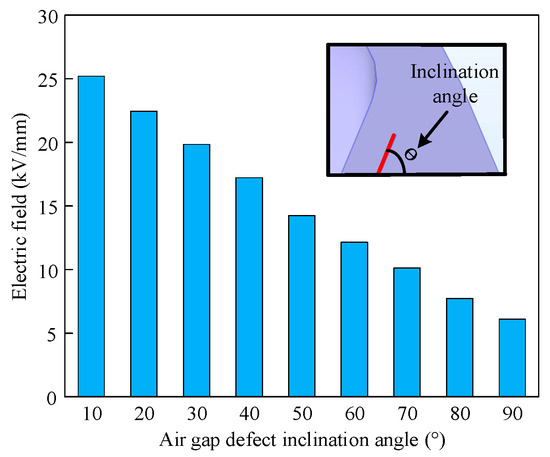
Figure 12.
Relationship between the maximum electric field strength and the inclination angle of air gap defect B1.
As shown in Figure 12, the distortion capacity of the air gap defect diminishes as the angle between it and the conductor increases. To better predict the effect of different tilt angles on electric field strength, the study fitted the relationship between tilt angle and maximum electric field strength based on the data in Figure 12.
As shown in Equation (6), when the inclination angle is between 10° and 90°, the corresponding electric field strength E can be calculated by substituting the inclination angle into Equation (6). Through verification, the equation can accurately predict the influence of different inclination angles on the electric field:
In Equation (6), E denotes the electric field strength (kV/mm) and θ is the angle of inclination formed between the air gap defect B1 and the conductor (°).
4.2.3. Air Gap Defect B2 Within the Insulator Away from the Conductor
The electric field simulation results for air gap defect B2 are shown in Figure 13. The most severe electric field distortion occurs at both ends of the air gap defect, with maximum field strengths of 5.73 kV/mm at 20 mm length and 6 kV/mm at 40 mm length. For B2 defects, the electric field distortion capability increases with defect length.
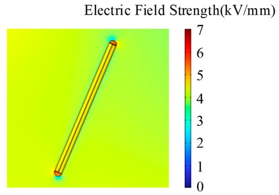
Figure 13.
Electric field strength distribution around 20 mm air gap defect B2.
4.2.4. Air Gap Defect B3 Within the Insulator Away from the Conductor
The results of the electric field simulation for the air gap defect B3 are shown in Figure 14. The most severe electric field distortion occurs at the top of the air gap defect; the maximum field strength is 16.76 kV/mm at 20 mm length and 14.83 kV/mm at 40 mm length. For the B3 defects, the ability of electric field distortion decreases with the increase in the defect length for both 20 mm and 40 mm lengths.
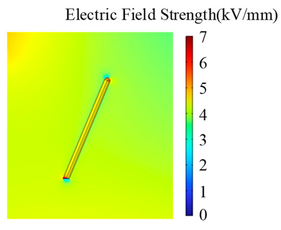
Figure 14.
Electric field strength distribution around 20 mm air gap defect B3.
As shown in Table 3. Of the various types of air gap defect, an unsmooth air gap has the highest maximum electric field strength due to its small radius of curvature and the strong electric field concentration effect. This results in a localized electric field at its tip that is much higher than the average field strength. This high local electric field accelerates electron avalanches, triggering avalanche discharges rapidly and increasing the likelihood of potential failures.
Table 3.
Maximum electric field strength of different air gap defects inside insulator.
4.3. Surface Void Defect C 150 mm from Conductor
The electric field simulation results for insulator surface with elliptical defect C is shown in Figure 15a. The electric field strength is mainly concentrated at the interface between the insulator surface and the defect, likely due to tip formation at the junction where the field concentration effect is stronger. Compared to the bottom of the defect, both sides of the defect cause greater field distortion, with the conductor proximal end exhibiting stronger distortion capability. Figure 15b shows the geometric schematic of the void defect.
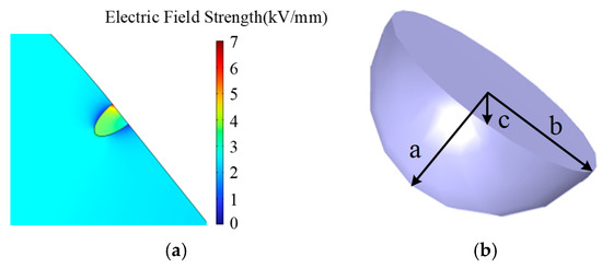
Figure 15.
(a) Electric field strength distribution around air gap defect C (a = 2 mm, b = 1 mm, c = 1 mm). (b) Geometric schematic of the void defect.
To investigate the influence of elliptical surface void dimensions on electric field distortion capability, the simulation varied three radii (a, b, c) of the ellipse. Specifically, it examined the effect of radius a (ranging from 1 mm to 10 mm) while maintaining radii b and c constant at 1 mm. The results are shown in Figure 16, where the electric field distortion capability increases slightly with the increase in radius a but the variation is not significant.
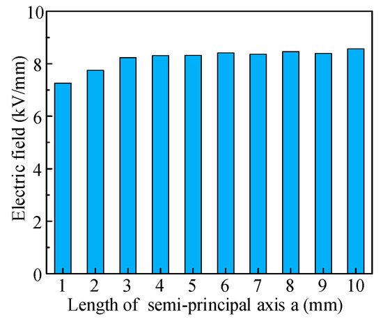
Figure 16.
The influence of radius a on electric field strength (b = 1 mm, c = 1 mm).
Specifically, it examined the effect of radius b (ranging from 1 mm to 10 mm) while maintaining radii a and c constant at 1 mm. As shown in Figure 17, the electric field strength gradually weakens by increasing radius b, which indicates that larger b values correspond to a reduced electric field distortion capability. The size of radius b of the elliptical defects may affect the angle formed by the defects and insulators. A change in the angle leads to a change in the strength of their electric field, and a change in radius b affects the size of the defects at the same time, thus affecting the distribution and strength of the electric field.
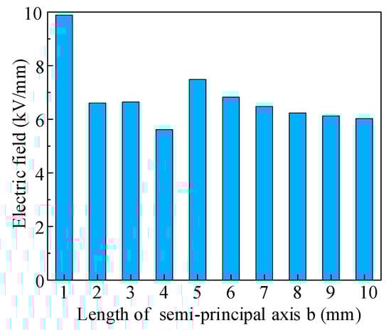
Figure 17.
The influence of radius b on electric field strength (a = 1 mm, c = 1 mm).
As shown in Figure 18, the electric field strength exhibits a gradual increasing trend with the increase in radius c. Compared with radii a and b, radius c demonstrates the strongest electric field distortion capability, reaching maximum distortion when radius c is 10 mm with a peak electric field strength of 18.70 kV/mm.
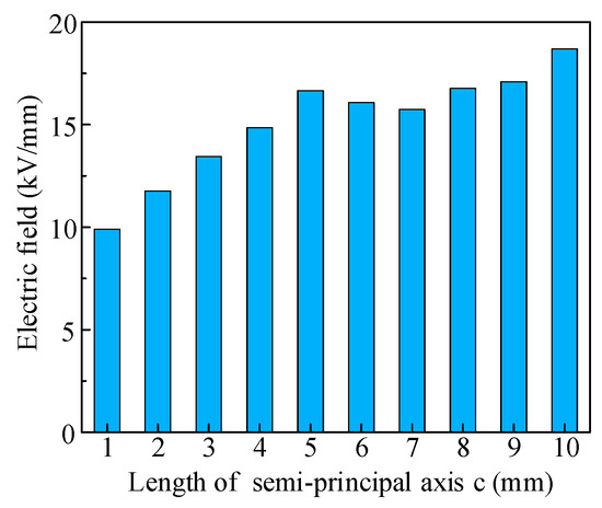
Figure 18.
The influence of radius c on electric field strength (a = 1 mm, b = 1 mm).
As shown in Figure 19 and Figure 20, the curves illustrate the variation in electric field strength along the arc length of insulator surfaces with different defects. The direction of the arrow indicates the direction of arc length increase. It can be observed that the minimum electric field strength occurs near the enclosure end of the defect, while the maximum appears adjacent to the conductor. Significant fluctuations in electric field strength around the defect area may readily trigger surface flashover, leading to insulation failure and potential hazards.
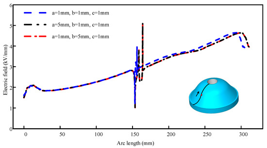
Figure 19.
Variation curve of electric field strength versus arc length.
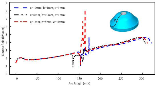
Figure 20.
Curve diagram of the relationship between arc length and electric field strength.
As shown in Table 4, the influence of radius a of the void defect C on the electric field strength is relatively stable. As radius a increases, the maximum electric field strength gradually increases, but the change is not dramatic. The influence of radius b on the electric field strength is more complicated. With the increase in radius b, the maximum electric field strength decreases first and then increases, then decreases. When the radius is 1 mm, the electric field distortion ability is the strongest. Radius c has a great influence on the electric field intensity, and the maximum electric field intensity increases with the increase in radius c.
Table 4.
Maximum electric field strength of different void defect radius (kV/mm).
4.4. Effect of Insulator Surface Crack on the Magnitude of the Electric Field Strength
This paper compares the effects of insulator surface cracks on electric field strength at different locations. As shown in Figure 21. The cracks considered are 30 mm long, 10 mm deep and 1.5 mm wide, and are located 65 mm, 85 mm and 150 mm from the conductor, respectively.
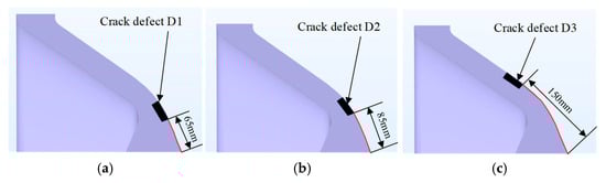
Figure 21.
The schematic diagram of surface crack defects at different positions relative to the conductor. (a) Distance to the conductor 65 mm; (b) Distance to the conductor 85 mm; (c) Distance to the conductor 150 mm.
4.4.1. Surface Crack Defect D1 65 mm from Conductor
The electric field simulation results for surface crack defect D on the insulator are shown in Figure 22a. The electric field is primarily concentrated at the two ends and the tip of the crack defect, likely due to the stronger field concentration effect caused by tip formation at the junctions. Figure 22b illustrates the geometric schematic of crack defect D.
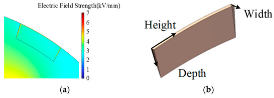
Figure 22.
(a) Electric field strength distribution around crack defect D. (b) Geometric schematic of the crack defect D.
As illustrated in Figure 23, the magnitude of the electric field strength is distributed across each section. Clearly, the strength of the electric field strength at the base of the crack defect exceeds that of the surrounding insulator surface. The maximum strength is recorded at the base of the crack in close proximity to the conductor, with a value of 14.94 kV/mm. The surface crack is closer to the position of the guide conductor, and the electric field gradient is larger, resulting in larger local field strength distortion. Figure 23a shows a plot of the resultant electric field strength on the insulator surface and Figure 23b shows a line plot of the electric field strength along the defect path on the insulator surface. The direction indicated by the arrows in the figure is the direction of arc length increase.
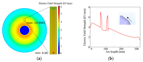
Figure 23.
(a) Results of electric field simulations performed for a crack defect D1 on the insulator surface. (b) Electric field line diagram of surface crack defect D1 of the insulator.
4.4.2. Surface Crack Defect D2 85 mm from Conductor
The results pertaining to the electric field on the insulator surface located 85 mm from the conductor with surface cracks are presented in Figure 24. The direction indicated by the arrows in the figure is the direction of arc length increase. It is evident from the figure that the electric field strength of the insulator at the crack defects is considerably higher than that at the non cracked area. Concurrently, the electric field around the surface cracks undergoes a substantial distortion, particularly at the top and bottom of the cracks, reaching the maximum value of the electric field distortion. The maximum value that can be achieved is 13.67 kV/mm. Compared to the crack defect D1, the surface crack D2 is further away from the conductor location and has a smaller potential gradient, resulting in a smaller local field strength distortion capability than the crack defect D1.
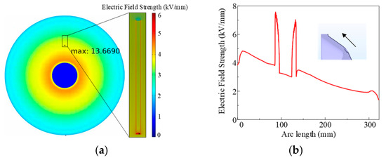
Figure 24.
(a) Results of electric field simulations performed for a crack defect D2 on the insulator surface. (b) Electric field line diagram of surface crack defect D2 of the insulator.
4.4.3. Surface Crack Defect D3 150 mm from Conductor
As illustrated in Figure 25, the magnitude of the electric field strengths within each component is shown. The direction indicated by the arrows in the figure is the direction of arc length increase. The intensity of the electric field strength at the base of the crack defect exceeds that observed at the surrounding insulator surface. The maximum strength is recorded at the base of the crack in close proximity to the conductor: 12.50 kV/mm. As illustrated in Figure 26, Compared with the crack defect D1 and crack defect D2, the surface crack D3 is located farther away from the conductor and has a smaller electric field gradient, resulting in a smaller local field strength distortion capability than the crack defects D1 and D2.
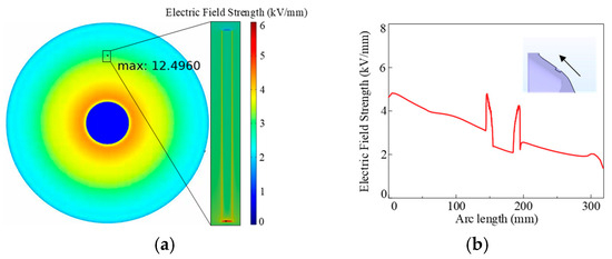
Figure 25.
(a) Results of electric field simulations performed for a crack defect D3 on the insulator surface. (b) Electric field line diagram of surface crack defect D3 of the insulator.
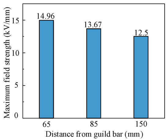
Figure 26.
Maximum electric field strength as a function of the distance of surface crack defect from the conductor.
A comparative analysis reveals that the highest field strength at the bottom of the crack defect is 14.94 kV/mm 65 mm from the conductor. The highest field strengths at 85 mm and 150 mm are 13.67 kV/mm and 12.50 kV/mm, respectively. The closer to the conductor, the greater the electric field gradient and the greater the distortion of the electric field around it by the cleft defect. The proximity of the surface crack defect to the conductor is pivotal in determining its impact. Furthermore, the field strength at the extreme point is particularly significant. It is important to note that the field strength at the bottom of the crack defect exceeds that of the surrounding insulator surface, which may cause flashover along the surface.
The field strength at the bottom of the defective area is higher than at the surface of the surrounding insulator, particularly at the end of the defective area near the conductor where the maximum field strength is located.
5. Conclusions
This paper proposes a simulation model for analyzing the electric field strength distribution of basin insulator, which is constructed based on the benchmark operating conditions of 550 kV GIL and aims to investigate the effects of various insulator defects on their insulation performance. The study includes small internal air gap defects, elliptical cavity defects, and surface crack defects in the insulator. By systematically comparing the influence of defect location and geometry on electric field strength, the following conclusions are drawn.
Internal air gap defects in the insulator significantly alter the electric field distribution, concentrating the electric field at the defect tip and creating localized regions with field strengths far exceeding the average. For small air gap defects near the conductor, longer lengths result in weaker electric field distortion capability, while radius has a relatively minor effect.
For elongated air gap defects near the conductor, longer lengths lead to stronger distortion capability. Smooth air gap defects away from the conductor show weak length dependent distortion capability, whereas unsmooth air gap defects away from the conductor exhibit decreasing distortion capability with increasing length. Analysis indicates that defect geometry is a key influencing factor, with more irregular surfaces causing more pronounced electric field concentration. Unsmooth air gaps, due to their small radius of curvature, generate strong field concentration effects, producing localized field strengths much higher than the average. This high local field accelerates electron avalanches, rapidly triggering avalanche discharges and increasing failure risks.
For elliptical surface crack defects on the insulator, the maximum electric field strength is primarily concentrated at the defect boundary near the conductor side, with radius a having the least influence and radius c exhibiting the strongest impact on field distortion capability, showing an increasing maximum field strength with larger radius c. For surface crack defects, the electric field strength at the crack bottom exceeds that of the surrounding insulator surface, with the maximum field strength occurring at the crack bottom closest to the conductor side.
At the same time, by fitting the sizes of different types of defects to the maximum electric field intensities they generate, the corresponding relationships between them can be obtained, enabling the prediction of how changes in defect size affect the insulation performance of basin insulators.
Currently, this study analyzes the static effects of defects on electric fields using the finite element method (FEM). However, the actual operation of GIL equipment requires consideration of multi-field coupling effects, such as temperature fluctuations and mechanical vibrations. In future work, an “electromagnetic–thermal–structural” multi-physics coupling model can be developed to further enhance predictions of basin insulators’ insulation performance.
Author Contributions
Z.Y. Conceptualization, investigation, writing original draft and funding acquisition; Y.W. Methodology, software, formal analysis, writing—review and editing; J.L. Methodology, formal analysis; H.L. writing—review and editing; L.L. software, validation, date, curation and visualization. X.L. Resources, project administration and supervision. All authors have read and agreed to the published version of the manuscript.
Funding
This research was funded by Key Science and Technology Project of State Grid Jiangsu Electric Power Co., Ltd. (J2024121).
Data Availability Statement
The original contributions presented in the study are included in the article, further inquiries can be directed to the corresponding author.
Conflicts of Interest
Authors Zhuoran Yang, Yue Wang, Jian Liu, Hongze Li and Lixiang Lv were employed by the company State Grid Nanjing Power Supply Company. The authors declare that this study received funding from Key Science and Technology Project of State Grid Jiangsu Electric Power Co., Ltd. The funder was not involved in the study design, collection, analysis, interpretation of data, the writing of this article or the decision to submit it for publication. The remaining authors declare that the research was conducted in the absence of any commercial or financial relationships that could be construed as a potential conflict of interest.
References
- Xiao, D.M.; Yan, J.D. Application and development of gas insulated transmission lines (GIL). High. Volt. Eng. 2017, 43, 699–707. [Google Scholar] [CrossRef]
- Qi, B.; Zhang, G.X.; Li, C.R.; Gao, C.J.; Zhang, B.Y.; Chen, Z.Z. Research status and application prospects of gas insulated metal enclosed transmission lines. High. Volt. Tech. 2015, 41, 1466–1473. [Google Scholar] [CrossRef]
- Li, X.L.; Wan, M.; Yan, S.Y.; Lin, X. Temperature and electric field distribution characteristics of a DC GIL basin type spacer with 3D modelling and simulation. Energies 2021, 14, 7889. [Google Scholar] [CrossRef]
- Tian, F.Y.; Hao, Y.P.; Zuo, Z.Y.; Zheng, Y.; He, W.M.; Yang, L.; Li, L.C. An Ultrasonic Pulse Echo Method to Detect Internal Defects in Epoxy Composite Insulation. Energies 2019, 12, 4804. [Google Scholar] [CrossRef]
- Liu, T.; Sun, H.; Li, G.; Zhang, Y.; Wang, J.; Xiao, J.; Lu, Y.; Niu, C.; Wu, Y. Decay characteristic of gas arc in C4F7N/N2 and C4F7N/CO2 gas mixture by Thomson scattering. J. Phys. D Appl. Phys. 2024, 58, 045203. [Google Scholar] [CrossRef]
- Li, J.H.; Han, X.T.; Liu, Z.H.; Li, Y.M. A review of partial discharge detection techniques for electrical equipment. High. Volt. Technol. 2015, 41, 2583–2601. [Google Scholar] [CrossRef]
- Duan, Y.M.; Yang, H.; Wang, X.; Hang, J.; Zhao, S.R.; Zhou, F.S.; Gao, C. Research on Crack Defect Propagation Behavior of Epoxy Resin Material for Basin insulator Based on Johnson Cook Model. Mater. Rep. 2025, 39, 261–267. Available online: https://link.cnki.net/urlid/50.1078.TB.20250318.1505.004 (accessed on 7 October 2025).
- Liu, J.H.; Guo, C.X.; Yao, M.; Wang, Y.J.; Huang, C.J.; Jang, X.C. Analysis of the propagation path of partial discharge electromagnetic waves in GIS. High. Volt. Technol. 2009, 35, 1044–1048. [Google Scholar] [CrossRef]
- Wang, H.R.; Guo, Z.H.; Zhang, S.Y.; Du, J.Q.; Peng, Z.R.; Liu, P. Influence of defects on the electric field distribution of ultra high voltage AC basin type insulator. High. Volt. Technol. 2018, 4, 982–992. [Google Scholar] [CrossRef]
- Wang, H.M.; Ding, D.W.; Jia, Z.J.; Tang, M.Z.; Zhao, C.H.; Tang, Z.G. Study on the long intermittent discharge characteristics of GIS basin type insulator surface defects under constant pressure. Proc. CSEE 2018, 38, 6188–6194. [Google Scholar] [CrossRef]
- Chang, W.Z.; Bi, J.G.; Liu, S.P.; Yuan, S.; Zhou, H.Y.; Du, F.; Ma, G.M. Electric field simulation of typical defects in GIS basin type insulator. High. Volt. Appar. 2018, 54, 138–143. [Google Scholar] [CrossRef]
- He, B.N.; Kong, J.; Jiang, R.Z.; Ning, J.X.; Wang, L.M.; Xie, Y.D.; Huang, G.C. Electric field distribution simulation study under metal wire defects of basin type insulator. Insul. Mater. 2021, 54, 39–44. [Google Scholar] [CrossRef]
- Ueta, G.; Wada, J.; Okabe, S.; Miyashita, M.; Nishida, C.; Kamei, M. Insulation characteristics of epoxy insulator with internal void shaped micro defects, IEEE Trans. Dielectr. Electr. Insul. 2013, 20, 535–543. [Google Scholar] [CrossRef]
- Qi, B.; Li, C.R.; Hao, Z.; Geng, B.B.; Xu, D.G.; Liu, S.Y.; Deng, C. Phenomenon and characteristics of surface partial discharge development along fixed metal particles on GIS insulator. Proc. CSEE 2011, 31, 101–108. [Google Scholar] [CrossRef]
- Zhou, Q.; Tang, J.; Tang, M.; Xie, Y.B.; Liu, M.J. Mathematical model of partial discharge ultra high frequency for four typical defects in GIS. Proc. CSEE 2006, 08, 99–105. [Google Scholar] [CrossRef]
- Ding, D.W.; Gao, W.S.; Liu, W.D. Analysis of typical defects in GIS using ultra high frequency method. High. Volt. Technol. 2011, 37, 706–710. [Google Scholar] [CrossRef]
- Zou, Z.Y.; Hao, Y.P.; Tian, F.; Zheng, Y.; He, W.M.; Yang, L.; Li, L.C. An Ultrasonic Longitudinal Through Transmission Method to Measure the Compressive Internal Stress in Epoxy Composite Specimens of Gas Insulated Metal Enclosed Switchgear. Energies 2020, 13, 1248. [Google Scholar] [CrossRef]
- Liu, T.; Sun, H.; Zhang, Y.; Xiao, J.; Lu, Y.; Niu, C.; Wu, Y. Post arc electron density measurement in SF6 and SF6/CO2 mixture arcs using Thomson scattering. Spectrochim. Acta Part. B At. Spectrosc. 2025, 229, 107196. [Google Scholar] [CrossRef]
- Chen, C.; Liang, X.Y.; Zhang, M.W.; Liu, P.; Peng, Z.R. Ultrasonic Intelligent Diagnostic Method for the Internal Defects in Ultra-High Voltage Basin Insulators Using Improved YOLOv8. IEEE Trans. Dielectr. Electr. Insul. 2025. [Google Scholar] [CrossRef]
- He, B.N.; Kong, J.; Ning, J.X.; Wang, Z.Z.; Wang, L.M.; Xie, Y.D.; Hung, D.C. Electric field simulation analysis of basin type insulator with bubble defects. Insul. Mater. 2019, 52, 86–92. [Google Scholar] [CrossRef]
Disclaimer/Publisher’s Note: The statements, opinions and data contained in all publications are solely those of the individual author(s) and contributor(s) and not of MDPI and/or the editor(s). MDPI and/or the editor(s) disclaim responsibility for any injury to people or property resulting from any ideas, methods, instructions or products referred to in the content. |
© 2025 by the authors. Licensee MDPI, Basel, Switzerland. This article is an open access article distributed under the terms and conditions of the Creative Commons Attribution (CC BY) license (https://creativecommons.org/licenses/by/4.0/).