Article

Non-Isolated High Step-Up DC-DC Interleaved Boost Converter Based on Coupled Inductors and Voltage Multiplier Cells

by
Thaís Carvalho Salvador
1,
Rafael Mario da Silva
2,
Waner Wodson Aparecido Goncalves Silva
2,
Nedson Joaquim Maia
1,
Fernando Lessa Tofoli
3,* and
Enio Roberto Ribeiro
1
1
Institute of System Engineering and Information Technology, Federal University of Itajubá, Itajubá 37500-176, Brazil
2
Campus Itabira, Federal University of Itajubá, Itabira 35903-087, Brazil
3
Department of Electrical Engineering, Federal University of São João del-Rei, São João del-Rei 36307-352, Brazil
*
Author to whom correspondence should be addressed.
Energies 2025, 18(19), 5199; https://doi.org/10.3390/en18195199
Submission received: 7 August 2025 / Revised: 11 September 2025 / Accepted: 24 September 2025 / Published: 30 September 2025

Abstract

This work introduces a non-isolated high step-up dc-dc interleaved boost converter combining magnetic coupling and voltage multiplier cells (VMCs). The proposed topology features a transformer with two primary windings of equal turns, interconnected to each other, enabling improved current sharing, and multiple secondary windings that contribute to extending the voltage gain. A three-winding coupled inductor is integrated into the design, while VMCs not only boost the output voltage but also significantly reduce the voltage stresses on the switches, eliminating the need for extreme duty ratios. The converter exhibits inherent modularity, allowing for voltage gain adjustments either through the turns ratio of the coupled inductor or by incorporating additional VMCs. An in-depth analysis of the topology is derived, and an experimental prototype rated at 48 V/400 V, 25 kHz, and 1 kW is implemented to verify and validate the theoretical claims, achieving an efficiency of 95.12% at full-load conditions.

1. Introduction

Several modern applications rely on dc-dc converters, such as general-purpose switch-mode power supplies (SMPSs), electric vehicles (EVs), uninterruptible power systems (UPSs), renewable energy conversion systems, and telecommunications, among others [1]. When galvanic isolation is not a mandatory requirement, non-isolated high step-up dc-dc converters are interesting choices to extend the voltage gain and achieve high power density rather than using high-frequency transformers [2].
In several applications, including grid-connected and standalone photovoltaic (PV) systems, such converters play a crucial role in supplying a cascade inverter with a high dc-link voltage, thereby eliminating the need to connect multiple dc voltage sources, such as PV modules or batteries, in series [3]. According to [4], to achieve typical root mean square (rms) ac voltages of 127 V or 220 V, dc-link voltages of approximately 250 V or 400 V are necessary, respectively, with these ratings considered conservative. As for three-phase systems, dc-link voltages of around 400 V or 800 V are typically required to produce rms phase voltages of 127 V or 220 V, respectively.
Notably, the conception of novel non-isolated high step-up converters has been a hot topic in power electronics research. According to [5], several techniques can extend the conversion ratio of basic dc-dc converter topologies, such as voltage lifting, switched capacitors, switched inductors, magnetic coupling, and voltage multiplier cells (VMCs), as well as a combination of multiple solutions. For instance, combining switched capacitors and coupled inductors with the conventional boost converter, as demonstrated in [6,7], results in an extended voltage gain and reduced stress on the semiconductor devices. Similarly, the family of converters based on magnetic coupling and ladder switched capacitors, as proposed in [8], can achieve good trade-offs between voltage gain and component count. Another interesting possibility for improving power density in such structures involves the use of wide-bandgap semiconductors and the adoption of magnetic integration approaches, as discussed in [9,10], respectively.
In this sense, a plethora of novel structures have been proposed in the literature, primarily aiming to achieve the highest possible voltage gain. However, the comprehensive analysis presented in [11] showed that this is not the only aspect that matters, as distinct design trade-offs involving voltage gain, component count, semiconductor stresses, cost, and power density must also be taken into account.
The input currents of non-isolated high step-up converters are often high, even at low power ratings of around few hundred watts. This issue motivated the application of the interleaving concept to develop multi-phase structures capable of achieving partial ripple cancellation, high efficiency, and enhanced thermal distribution [12]. For instance, the six-phase interleaved boost converter proposed in [13] can achieve very high efficiency in a marine hybrid system powered by fuel cells. However, it cannot reach a high voltage gain. Conversely, the topology addressed in [14] integrates a voltage-lift capacitor and a VMC into a two-phase interleaved boost converter to mitigate this inconvenience, but some important drawbacks cannot be neglected. While the input current presents a large ripple, a clamping circuit is required to mitigate the high voltage spikes on the switches due to coupled windings associated with the input filter inductors. Despite requiring a low component count, the efficiency is around 92% at the rated power of 1000 W, rendering the topology unfeasible for high-power applications.
The interleaved boost converter proposed in [15] has the advantage of being a minimum-phase system without right-half-plane (RHP) zeros, operating over a wide duty cycle range with low voltage stress on the switch. While the converter was designed for a rated power of 200 W only, it cannot reach very high gains. Combining a voltage-lift capacitor and coupled inductors as in [16] offers enhanced voltage gain. Furthermore, an active clamping circuit allows for soft-switching operation of the converter, reaching a high efficiency of around 96.5% at 210 W.
The interleaved boost converter based on a built-in transformer, as presented in [17], significantly extends the voltage gain by employing two voltage-doubler circuits composed of diodes and capacitors on the secondary side. This configuration also recycles the energy stored in the transformer’s leakage inductance. Although the efficiency remains consistent over a wide load range, it reaches only 93% at the rated power of 200 W. Meanwhile, the high-gain interleaved dc-dc converter introduced in [18] relies on an asymmetric VMC (AVMC) and a lossless passive snubber. Compared to the classical interleaved boost converter, it can achieve much higher voltage gains due to the AVMC and a coupled inductor. It exhibits low input current ripple as a result of the interleaved structure, and the voltage stresses on both switches and diodes are substantially low, enabling the use of semiconductors with low on-resistance.
The two-switch boost converter based on a three-winding coupled inductor and a charge pump circuit introduced in [19] can achieve moderate voltage gain while incorporating important advantages such as magnetic integration. However, other drawbacks, such as large input current ripple and lack of a common ground connection, cannot be neglected in the design. Another configuration incorporating a built-in transformer and VMCs, assessed in [20], provides an extended voltage gain and high efficiency.
The configuration introduced in [21] relies on a VMC to obtain a voltage gain approximately three times greater than that of the traditional boost converter. Although its component count remains low, the approach is suitable only for modest conversion ratios. In contrast, the topology in [22] employs switched capacitors in conjunction with step-up cells to enhance the gain. However, the need for seven inductors renders the design bulky and unfeasible for practical applications.
To achieve higher conversion ratios, interleaved boost converters combined with coupled inductors have been investigated in the literature. By selecting appropriate turns ratios, excessively high duty ratios can be avoided, thereby reducing conduction losses in power switches. The converter analyzed in [23] exemplifies this approach by integrating two magnetically coupled windings into the input filter inductors, resulting in reduced voltage stress on the switches and a manageable component count. A similar architecture designed for PV systems is evaluated in [24]. While it exhibits high efficiency at around 900 W, the voltage gain remains below three, a performance already achievable with a conventional two-phase interleaved boost converter without the need for advanced step-up techniques or additional circuitry.
High voltage gains can also be achieved by combining coupled inductors with multiple passive elements, as demonstrated in [25]. Although this configuration provides a voltage gain close to 20, the experimental prototype operates at relatively low power levels and fails to achieve high efficiency under full-load conditions. Additionally, voltage multiplier rectifiers (VMRs) have been combined with coupled inductors in [26]. However, voltage imbalance across output capacitors remains a critical issue, limiting their applicability in real-world systems.
A design associating a VMC with a built-in transformer is proposed in [27]. Although the experimental results demonstrate satisfactory current sharing between the system phases, this behavior is not inherent in the topology and depends heavily on the precise matching of input filter inductors. A family of interleaved high step-up converters employing magnetic coupling is introduced in [28]. Despite voltage gains being proportional to the square of the duty cycle, potential drawbacks include a high component count, the need for active devices with distinct voltage and current ratings, and the lack of a common ground connection.
Another approach consisting of integrated coupled inductors and built-in transformers, as demonstrated in [29], can enhance the voltage gain while enabling optimization through turns ratio adjustments of the magnetic elements. However, the bulky nature of the resulting hardware restricts its application primarily to low-power systems. In contrast, the converter introduced in [30] adopts a series-stacked architecture to provide high step-up, but at the cost of a significantly higher component count.
The cascaded two-stage architecture presented in [31] achieves ultra-high voltage gain by combining advanced techniques such as interleaving, switched-capacitor networks, and magnetic coupling. Despite these innovations, its overall efficiency remains low, limiting its applicability in high-power scenarios. The structure employing two three-winding magnetic couplers and a pair of VMCs explored in [32] also achieves a high conversion ratio. However, the experimental results reveal significant voltage spikes on the active switches, primarily caused by the leakage inductance.
Overall, it is reasonable to state that non-isolated dc-dc interleaved boost converters available in the literature can be classified into three major groups:
(1)
Topologies with high or ultra-high voltage gain and rated power in the range of a few hundred watts, available in thousands of publications.
(2)
Topologies with low voltage gain and power levels ranging from a few kilowatts to tens of kilowatts, as seen in conventional interleaved converters without high step-up capability.
(3)
Topologies with high voltage gain and rated power in the range of a few kilowatts, which are addressed in a significantly smaller number of works.
In the context of the third group, this work presents a novel non-isolated high step-up dc-dc interleaved boost converter integrating magnetic coupling and voltage boosting techniques to enhance performance. The topology relies on a transformer with two primary windings of equal turns, interconnected to each other, with the aim to ensure balanced current sharing, yielding enhanced performance over conventional interleaved designs, as outlined in [33]. Multiple secondary windings contribute to an extended voltage gain without resorting to extreme duty ratios. Additionally, a three-winding coupled inductor is incorporated to further enhance energy transfer, while VMCs not only contribute to increasing the output voltage but also significantly reducing voltage stress on the switches. One of the key advantages lies in the converter’s modularity, which allows for a flexible design through adjustments in the number of secondary windings, the turns ratio of the coupled inductor, or the number of VMCs. This results in low current and voltage stress on the switches and diodes, high efficiency, and moderate component count.
These features yield an efficient solution for both standalone and grid-connected single-phase inverters, especially those operating at dc voltage levels around 400 V, as commonly required in PV systems. The converter is also suitable for battery-powered systems involving output voltages in the range of several hundred volts. Furthermore, a promising application lies in connecting the converter directly to the dc bus of a microgrid, thereby eliminating redundant power processing stages in renewable energy systems such as PV and fuel cell-based architectures.
The structure of this article is outlined as follows. Section 2 describes the interleaved boost converter, including a thorough theoretical analysis in continuous conduction mode (CCM) and a comprehensive design procedure comprising all power stage elements. Section 3 compares the proposed structure with other similar counterparts found in the recent literature. Section 4 presents the experimental results obtained from a laboratory prototype rated at 48 V/400 V, 25 kHz, and 1 kW. Finally, Section 5 summarizes the main findings of this study.

2. Proposed Non-Isolated High Step-Up Interleaved Boost Converter

Figure 1 depicts the proposed high step-up converter, which is feasible for high-power, high-current applications. It relies on a transformer whose primary windings, with equal numbers of turns N1p1 and N1p2, are interconnected to each other. It is worth noting that magnetic coupling in this case ensures improved current sharing compared to conventional two-phase interleaved converters because the primary windings have the same impedance, as demonstrated in [34].
It is also possible to couple multiple secondary windings with turns N1s1N1sn to the transformer, associated with diodes Ds1Dsn and capacitors Cs1Csn, aiming to extend the voltage gain. Two branches composed of switches S1, S2 and diodes D1, D2 operate in an interleaved manner, relying on gating signals shifted by 180°. A three-winding coupled inductor represented by N2p1, N2s1, and N2s2 offers another degree of freedom for increasing the output voltage. In turn, VMCs composed of diodes Dm1Dm(n+1) and capacitors Cm1Cm(n+1) allow for not only achieving a high gain, but also minimizing the voltage stresses on the switches as more VMCs are incorporated into the circuit. The topology also comprises the input voltage source Vi, the input filter inductor L1, the output filter capacitor Co, and the load Ro.

2.1. Qualitative Analysis

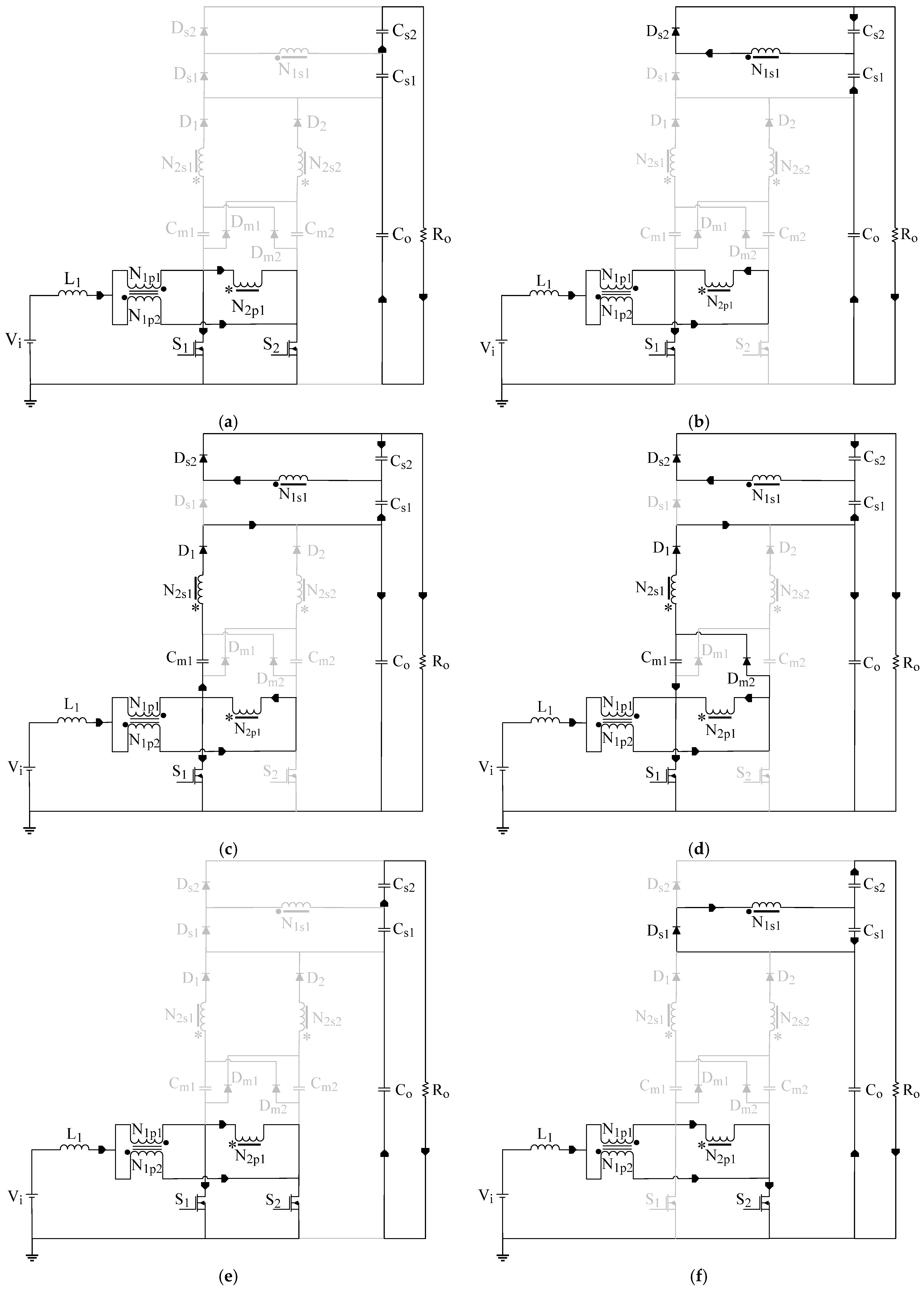
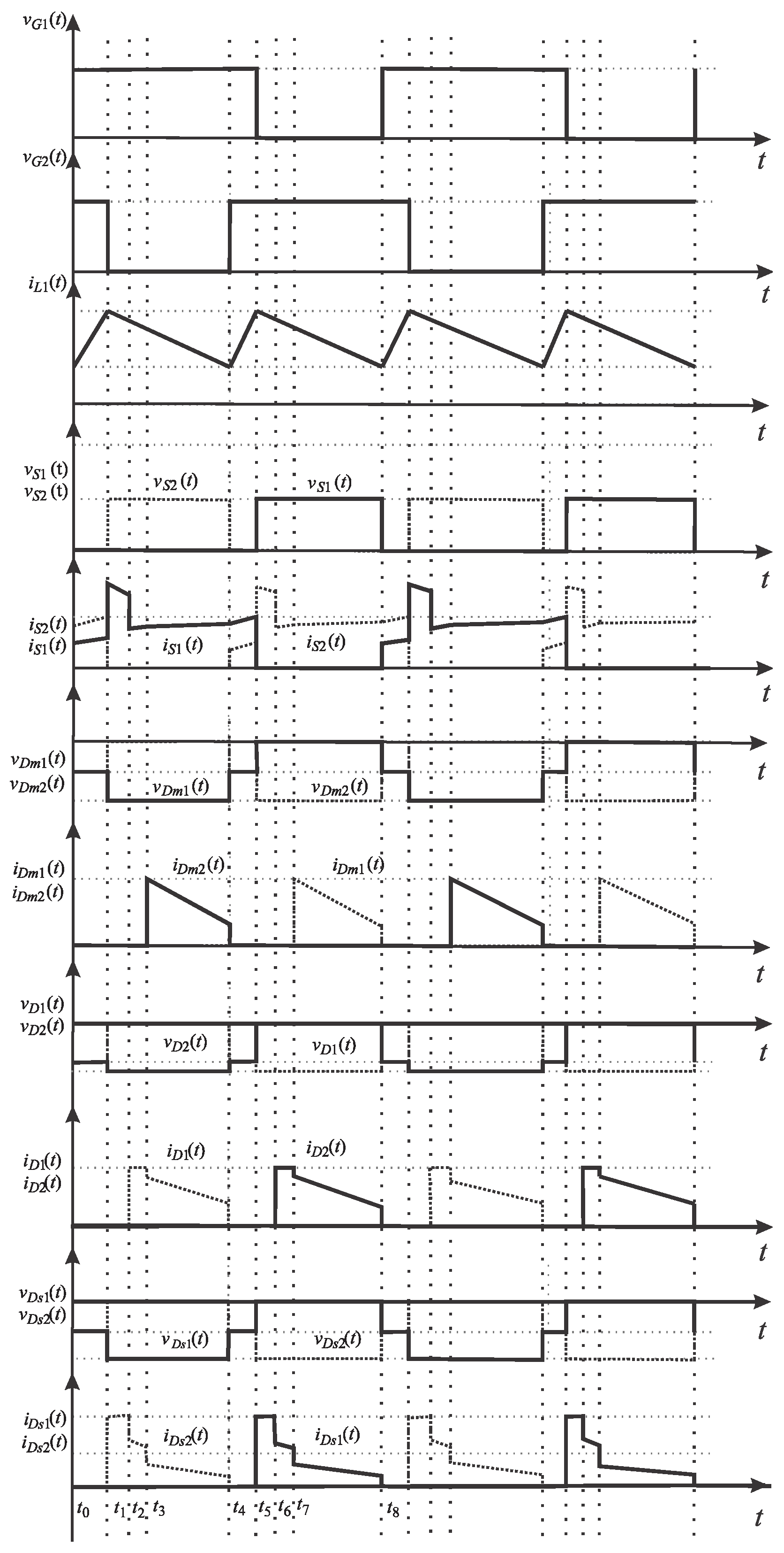
To perform the theoretical analysis of the converter operating in CCM, it is assumed that all power stage components are ideal; the primary windings of the transformer have the same number of turns so that the input current is equally shared between the phases; the converter operates in a steady-state, with a duty ratio D ≥ 0.5; the control signals of the active switches are phase-shifted by 180°; and the switching frequency remains constant. The corresponding operating stages and theoretical waveforms are illustrated in Figure 2 and Figure 3, respectively.
First stage [t0, t1] (Figure 2a): Both switches S1 and S2 are on. The current through inductor L1 increases linearly as it stores energy. Part of this current flows through one of the transformer windings (N1p1), shared between S1 and N2p1, while the other part, of equal magnitude, flows through N1p2 and S2, since N1p1 and N1p2 have the same number of turns. Meanwhile, diodes D1, D2, Dm1, Dm2, Ds1, and Ds2 are reverse-biased. The load is supplied due to the discharge of capacitors Co, Cs1, and Cs2. This stage ends when S2 is turned off.
The time interval Δt1, which defines this stage, can be calculated using (1).
Δ t 1 = t 1 t 0 = D 1 2 T s ,
where Ts is the switching period.
Second stage [t1, t2] (Figure 2b): Switch S1 remains on, while switch S2 is off. The voltage polarity across L1 is reversed, causing the current to decrease linearly. Diode Ds2 becomes forward-biased, while Ds1, Dm1, Dm2, D1, and D2 remain reverse-biased. Capacitor Cs2 begins charging, while Co and Cs1 continue discharging. This stage ends when D1 is forward-biased.
The time interval Δt2, which defines this stage, can be calculated using (2).
Δ t 2 = t 2 t 1 = C o C s 1 Δ V C o I o C o + C s 1 ,
where Io is the average output current and ΔVCo is the peak-to-peak voltage ripple across Co.
Third stage [t2, t3] (Figure 2c): Switches S1 and S2 are on and off, respectively. Diodes D1 and Ds2 are forward-biased, while diodes Ds1, D2, Dm1, and Dm2 remains reverse-biased. The voltage across L1 remains negative, causing the current to continue decreasing linearly. Capacitor Co begins charging, but Cs1 and Cs2 continue discharging and charging, respectively. This stage ends when Dm2 is forward-biased.
The time interval Δt3, which defines this stage, can be calculated using (3).
Δ t 3 = t 3 t 2 = C s 1 Δ V C s 1 I o ,
where ΔVCs1 is the peak-to-peak voltage ripple across Cs1.
Fourth stage [t3, t4] (Figure 2d): Switches S1 and S2 remain on and off, respectively. Diodes Dm2, D1, and Ds2 are forward-biased, but diodes Ds1, D2, and Dm1 reverse-biased. Capacitors Co and Cs2 charge, whereas capacitor Cs1 discharges into the load. This stage ends when S2 is turned on.
The time interval Δt4, which defines this stage, can be calculated using (4).
Δ t 4 = t 4 t 3 = T s D T s C s 1 Δ V C s 1 I o C o C s 1 Δ V C o I o C o + C s 1 ,
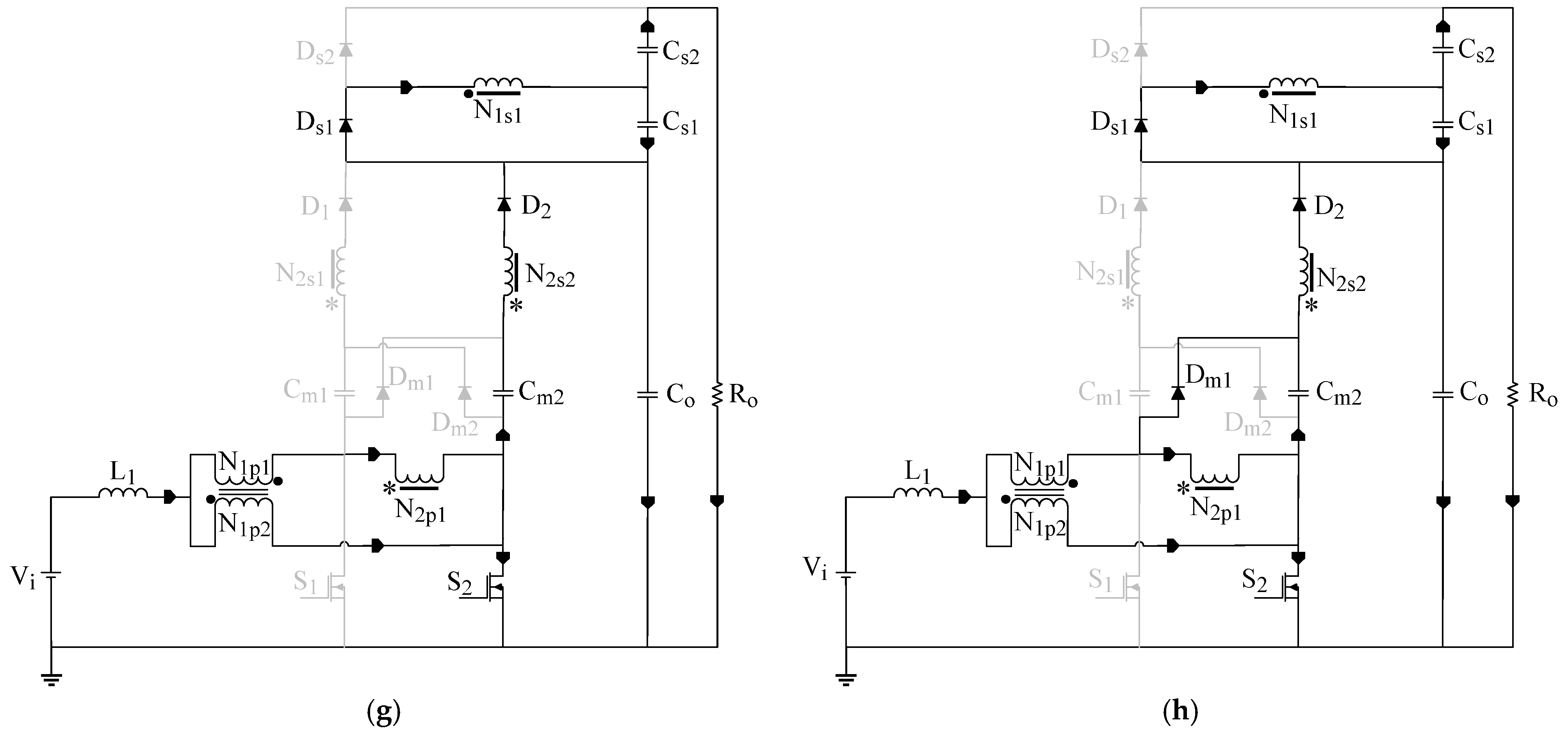
Fifth stage [t4, t5] (Figure 2e): This stage is similar to the first one and ends when S1 is turned off. Its respective time interval Δt5 is also defined by (1).
Sixth stage [t5, t6] (Figure 2f): This stage is complementary to the second one, with diode Ds1 becoming forward-biased instead of Ds2. This stage ends when D2 is forward-biased. Its respective time interval Δt6 is also defined by (2).
Seventh stage [t6, t7] (Figure 2g): This stage is analogous to the third one. Switches S1 and S2 remain off and on, respectively. Diode Ds1 is forward-biased, while diodes Ds2, D1, Dm1, and Dm2 remain forward-biased. The voltage across L1 is negative, as its current continues to decrease linearly. Capacitor Co begins charging, but Cs1 and Cs2 continue charging and discharging, respectively. This stage ends when Dm1 becomes forward-biased, with its respective time interval Δt7 given by (3).
Eighth stage [t7, t8] (Figure 2h): This stage is complementary to the fourth one. Switch S2 remain on, while switch S1 is off. Diodes Dm1, D2, and Ds1 are forward-biased. However, diodes Ds2, D1, and Dm2 are reverse-biased. Capacitors Co and Cs1 charge, while capacitor Cs2 discharges into the load. This stage ends when S1 is turned on again, with its respective time interval Δt8 given by (4).

2.2. Quantitative Analysis

By analyzing Figure 2 and Figure 3, it is possible to apply the volt-second balance principle to inductor L1 to obtain (5) and (6).
V L 1 = 2 T s 0 D T s T s 2 V i d t + 0 1 D T s V i V N 1 max d t = 0 ,
V i D T s T s 2 = V N 1 V i 1 D T s ,
where VL1 is the average voltage across L1, Vi is the input voltage, and VN1(max) represents the maximum voltage across the primary windings of the transformer. Therefore, the maximum voltage across the primary windings of the transformer is given by (7).
V N 1 max = V N 1 p 1 max = V N 1 p 2 max = V i 2 1 D .
Furthermore, the output voltage Vo is equal to the sum of the average voltages across capacitors Co, Cs1, and Cs2, corresponding to VCo, VCs1, and VCs2, respectively, according to (8).
V o = V C o + V C s 1 + V C s 2 .
It is also possible to calculate VCo, VCs1, and VCs2 from (9) and (10), where n1 and n2 account for the turns ratio of the transformer and coupled inductor, as defined by (11) and (12), respectively.
V C o = V i n 2 + m c 1 D ,
V C s 1 = V C s 2 = V i n 1 2 1 D ,
n 1 = N 1 s 1 N 1 p 1 ,
n 2 = N 2 s 1 N 2 p 1 = N 2 s 2 N 2 p 1 = L 2 s 1 L 2 p 1 = L 2 s 2 L 2 p 1 ,
where mc is the number of VMCs; N1p1 and N1s1 are the number of turns of the primary and secondary windings of the transformer, respectively; N2p1, N2s1, and N2s2 are the number of turns of the coupled inductor’s windings; and L2p1, L2s1, and L2s2 are the self-inductances of the coupled inductor’s windings.
Thus, substituting (9) and (10) into (8), it is possible to calculate the voltage gain GV of the ideal converter according to (13). If the leakage inductance of the coupled inductor (Llkg) is considered in the analysis, the gain will be obtained using (14).
G V = V o V i = n 1 + n 2 + m c 1 D ,
G V = V o V i = n 1 + L 2 s 1 L 2 p 1 + L l k g + m c 1 D .
The input filter inductance can be determined from (15).
L 1 = V o 1 D 2 D 1 2 f s Δ I L 1 n 1 + n 2 + m c ,
where ΔIL1 represents the peak-to-peak current ripple through L1 and fs is the switching frequency.
It is possible to determine Co, Cs1, and Cs2 from (16) and (17).
C o = P o D 1 D 2 V i f s Δ V o n 1 + n 2 + m c ,
C s 1 = C s 2 = D P o 1 D V i f s Δ V o n 1 + n 2 + m c ,
where ΔVo is the peak-to-peak output voltage ripple and Po is the output power.
The VMC’s capacitances Cm1 and Cm2 can be calculated from (18).
C m 1 = C m 2 = I L 1 1 D 4 f s Δ V C m ,
where IL1 is the average current through L1, which is equal to the average input current Ii; and ΔVCm represents the peak-to-peak voltage ripple across the multiplier capacitors.
The average and rms currents through the active switches are given by (19) and (20), respectively. Additionally, the voltage stress on the switch can be determined from (21).
I S 1 a v g = I S 2 a v g = I L 1 D + n 1 + n 2 2 n 1 + n 2 + m c ,
I S 1 r m s = I S 2 r m s = I L 1 5 D n 1 + n 2 + m c ,
V S 1 max = V S 2 max = V i 1 D .
The average and rms currents through the VMC’s diodes and output diodes are calculated from (22)–(27). The maximum reverse voltages across the diodes are given by (28)–(30).
I D 1 a v g = I D 2 a v g = I L 1 1 D 2 n 1 + n 2 + m c ,
I D s 1 a v g = I D s 2 a v g = I L 1 1 D n 1 + n 2 + m c ,
I D 1 r m s = I D 2 r m s = 3 I L 1 2 3 4 D 10 n 1 + n 2 + m c ,
I D s 1 r m s = I D s 2 r m s = 5 I L 1 2 3 4 D 6 n 1 + n 2 + m c ,
I D m 1 a v g = I D m 2 a v g = I L 1 1 D 2 n 1 + n 2 + m c ,
I D m 1 r m s = I D m 2 r m s = I L 1 2 3 4 D 3 n 1 + n 2 + m c ,
V D 1 max = V D 2 max = 2 n 2 + m c 2 V i 1 D ,
V D s 1 max = V D s 2 max = n 1 V i 1 D ,
V D m 1 max = V D m 2 max = 2 V i 1 D .

2.3. Small-Signal Modeling

The small-signal analysis of power electronic converters can be performed utilizing the well-established state-space averaging (SSA) technique proposed in [35]. However, this process becomes quite tedious and complex as the system order increases. Given this, the authors in [36] proposed a simplified, yet accurate solution based on the pulse-width modulation (PWM) switch model for modeling non-isolated high step-up dc-dc boost converters based on VMCs. Applying this methodology to the topology shown in Figure 1 yields (31)–(33), which represent the control-to-output transfer function vo(s)/d(s), the inductor-current-to-output transfer function vo(s)/iL(s), and the control-to-inductor-current transfer function iL(s)/d(s).
v o s d s = R o 1 D V o 2 I i L 1 s 4 L s s R o C o e q . + 1 + 1 D 2 R o ,
v o s i L s = R o 1 D V o 2 I i L 1 s 2 V o s R o C o e q . + 1 + 1 D R o I i ,
i L s d s = 2 V o s R o C o e q . + 1 + 1 D R o I i 4 L 1 s s R o C o e q . + 1 + 1 D 2 R o ,
where Co(eq.) is the equivalent capacitance corresponding to the series association of Cs1, Cs2, and Co.
It is possible to validate these equations by performing time-domain simulations and comparing the responses of the converter and the small-signal model. For this purpose, the rated operating conditions adopted in the design of the experimental prototype tested in Section 4 were adopted, corresponding to Vi = 48 V, Vo = 400 V, Po = 1000 W, fs = 25 kHz, D = 0.58, L1 = 50 µF, and Co(eq.) = 15 µF. Figure 4a shows that the response of the converter aligns well with that of the model representing vo(s)/d(s), when perturbing the rated duty ratio by +0.01, −0.01, and +0.05 at 100 ms, 200 ms, and 300 ms, respectively. Similarly, it is observed that vo(s)/iL(s) represents the converter accurately in Figure 4b. In this test, the rated input voltage is incremented by +0.01 V, −0.01 V, and +0.02 V at 100 ms, 200 ms, and 300 ms, respectively, which perturbs the inductor current as a consequence. Similarly, the inductor current follows iL(s)/d(s) in Figure 4c when the rated duty cycle is perturbed by −0.001, +0.002, and −0.003 at 100 ms, 200 ms, and 300 ms.

3. Comparison with Other Non-Isolated High Step-Up Interleaved Boost Converters

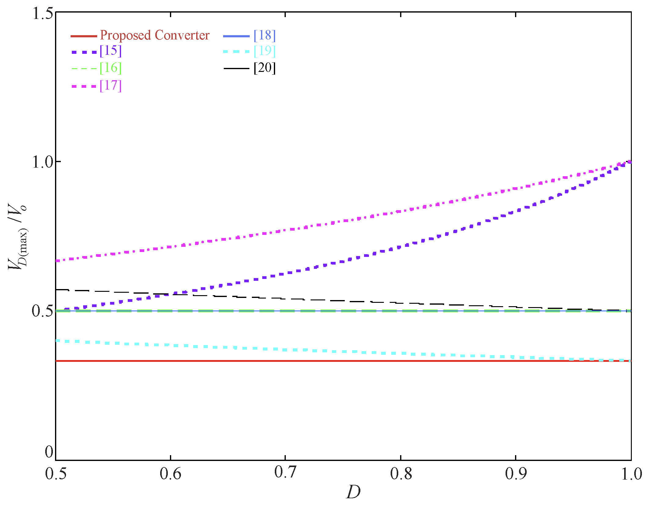
Table 1 compares some interleaved topologies based on coupled inductors found in the literature, where n is the turns ratio of the coupled inductors and NS is the number of secondary windings associated with the boost converter shown in Figure 1. Figure 5 depicts the voltage gain of the converter under analysis, while Figure 6 and Figure 7 represent the normalized voltage stresses on the switches and output diodes, respectively.
Despite combining the boost converter with auxiliary circuits in [15,16] provides voltage gain extension, the voltage stresses on the switches and output diode remain very high. Poor performance is also reported in [17], where the converter exhibits the lowest voltage and high normalized voltage stresses on the semiconductors. Conversely, the highest gain is obtained in [18], but the need for a clamping circuit to mitigate voltage spikes caused by the leakage inductance of the coupled inductor results in a high component count.
The converter proposed [19] requires few components, but the lack of a common ground connection, the need for isolated gate driver circuitry, and its modest voltage gain make it less appealing for practical applications. High voltage gain and low stresses on the switch are also obtained in [20]. However, this structure may suffer from significant voltage and current imbalance caused by the differential connection of two boost converters.
Unlike its counterparts, the proposed converter offers significant advantages, such as moderate voltage gain combined with a reasonable component count, low voltage stresses on switches and diodes, a common ground connection, enhanced current sharing due to magnetic coupling, inherent modularity associated with the possibility of adding more secondaries and VMCs. Notably, it is not intended to compete with other coupled-inductor-based topologies that can achieve ultra-high voltage gains, which in turn require a significantly higher number of components.

4. Experimental Results

Table 2 summarizes the specifications of the experimental prototype of the non-isolated high step-up interleaved boost converter, shown in Figure 8. It is worth mentioning that the rated operating conditions were defined similarly to those in [37]. Additionally, all experimental waveforms were measured using a four-channel digital oscilloscope, model TPS2024 by Tektronix.
Table 3 presents a comparison between calculated and experimentally measured parameters, showing good alignment and confirming the consistency of the theoretical analysis. Eventual differences are due to parasitics and layout issues associated with the prototype.
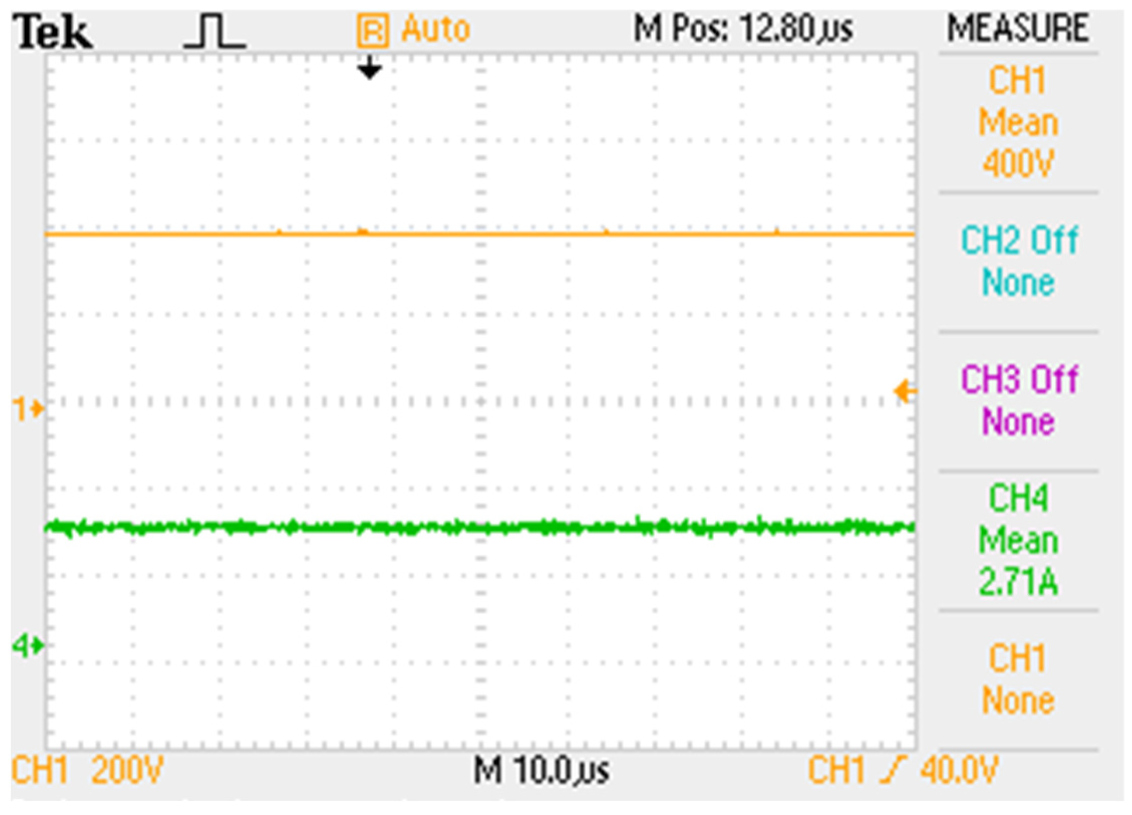
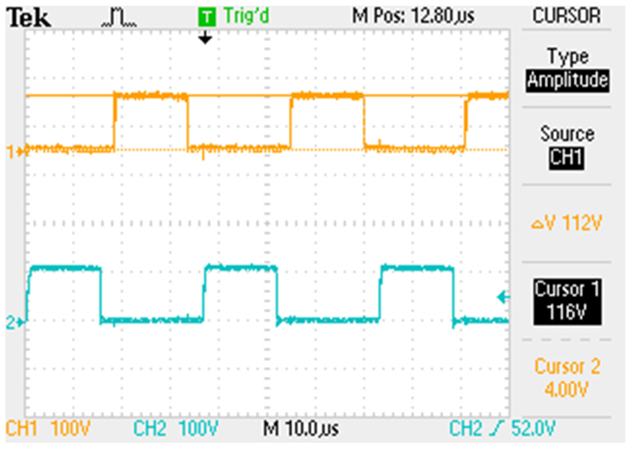
Figure 9 shows the output current and the output voltage, with the converter operating at the rated power condition. Figure 10 depicts the gate-to-source voltage and the input current. The current ripple is observed to remain within the desired specifications, with the input filter inductor operating at twice the switching frequency. Figure 11 shows the drain-to-source voltages, which are phase-shifted by 180°. Furthermore, the maximum voltage across the switches remains lower than one-third of the output voltage, while no significant voltage spikes exist. This behavior is attributed to the components of the VMC, which effectively ensures proper voltage clamping.
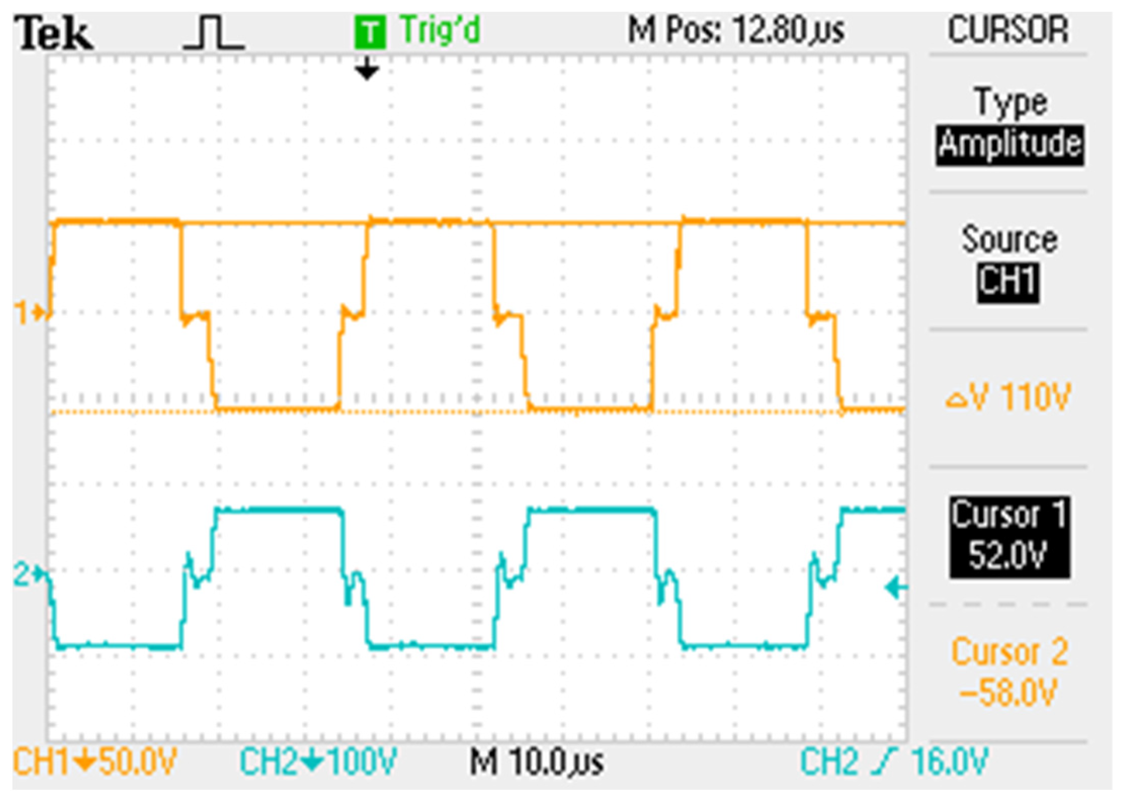
Figure 12 illustrates the voltages across one of the primary windings and the secondary winding of the transformer. Due to the identical impedance of the primary windings, the voltage across these windings is equal, and the converter achieves effective current sharing without requiring dedicated and complex control strategies. On the other hand, due to the turns ratio between the primary and secondary windings, the secondary voltage is higher, thus allowing for increasing the voltage gain.
Figure 13 shows the voltages across the output diodes D1 and D2, whose maximum value is lower than the output voltage. Similarly, the voltages across diodes Ds1 and Ds2 in Figure 14 are also phase-shifted by 180°, as expected.
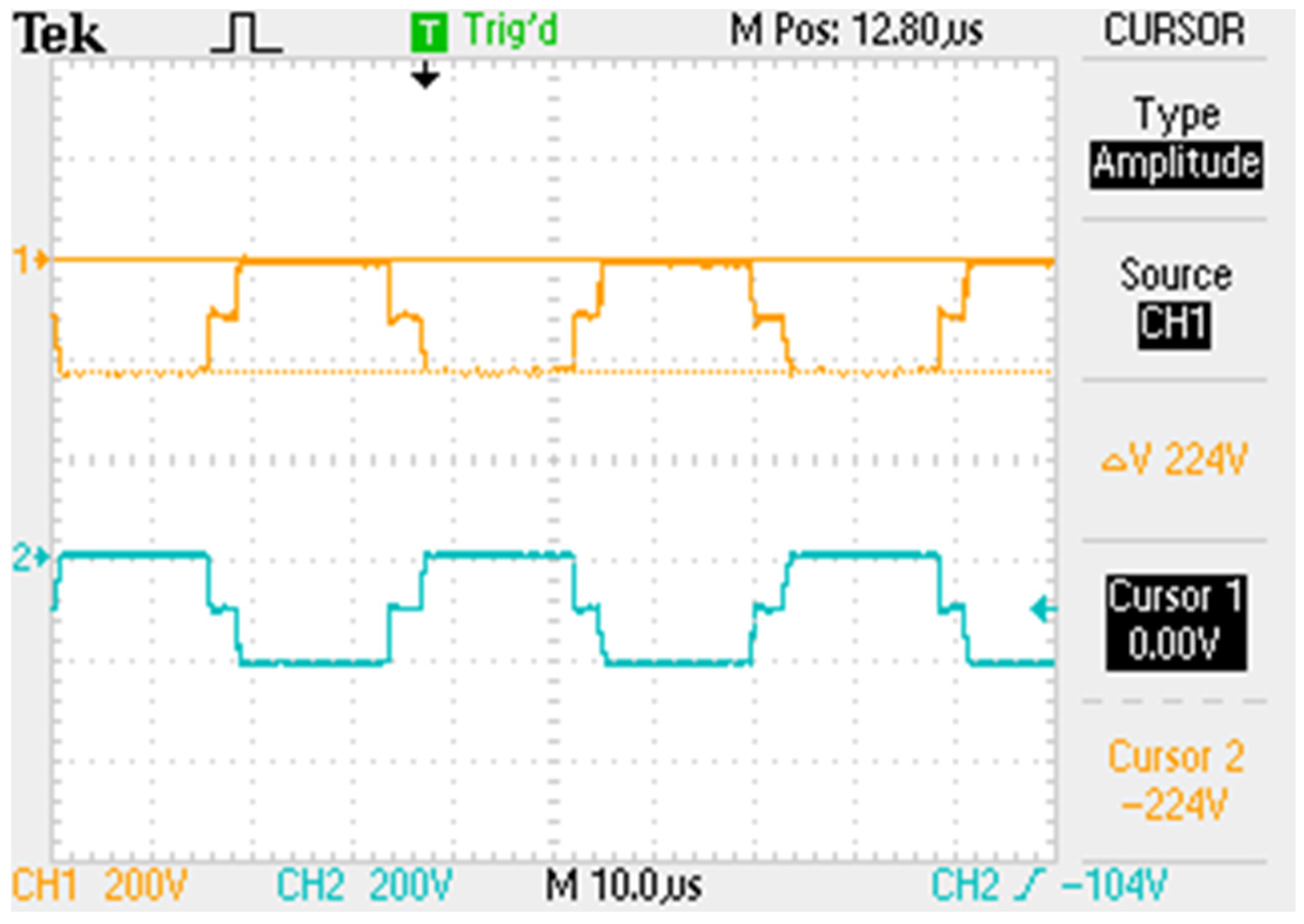
Figure 15 displays the voltages across the multiplier diodes Dm1 and Dm2. Such diodes are subjected to higher reverse voltages than their remaining counterparts due to the presence of adjacent capacitors in the VMCs. Nevertheless, the voltage stress is only slightly higher than half the output voltage.
Figure 16 shows the efficiency as a function of the output power, reaching a maximum of 96.31% around 800 W, with 95.12% around the rated power.
The total losses across all components, amounting to 47.9 W, were calculated based on experimentally measured current and voltage ratings. These calculations accounted for the characteristics of all semiconductors specified by commercial manufacturers and the properties of magnetic components determined during physical construction. The procedure adhered to expressions commonly found in power electronics textbooks, following the guidelines outlined in [37]. Notably, the loss breakdown shown in Figure 17 shows that the diodes and switches account for the major portions of losses, corresponding to 14.35 W and 13.47 W, respectively. Key improvements in overall efficiency could be achieved by employing devices with a lower drain-to-source on-resistance and forward voltage drop, for instance.

5. Conclusions

This work has presented a non-isolated high step-up dc-dc interleaved boost converter based on coupled inductors and VMCs, aimed at high-power, high-current applications. Prominent advantages of the topology include three possibilities to extend the voltage gain besides the duty ratio: the turns ratio of the transformer with multiple secondary windings, the turns ratio of the three-winding coupled inductor, and VMCs. The VMCs minimize the voltage stresses on semiconductors, keeping them below the output voltage and enabling the use of transistors with low drain-to-source on-resistance, reducing conduction losses. The design also eliminates the need for electrolytic capacitors, which typically exhibit higher equivalent series resistance (ESR) than film capacitors. Additionally, the primary windings of the transformer are designed to have identical impedance, ensuring better current sharing compared to conventional interleaved converters.
Although the proposed converter does not achieve the highest voltage gain compared to other similar topologies reported in the literature, it offers multiple solutions for increasing output voltage other than the duty cycle, enabling diverse design trade-offs. For example, adding more VMCs to the circuit can reduce voltage stresses without significantly affecting power density, as an alternative to increasing the turns ratio of magnetic elements. Overall, it can provide moderate voltage gains while achieving high efficiency across a wide load range, with the rated power reaching kilowatt levels.

Author Contributions

Conceptualization, F.L.T. and E.R.R.; methodology, F.L.T. and E.R.R.; validation, T.C.S.; formal analysis, T.C.S.; investigation, T.C.S.; supervision, F.L.T. and E.R.R.; visualization, R.M.d.S., W.W.A.G.S. and N.J.M.; writing—original draft preparation, T.C.S. and F.L.T.; writing—review and editing, F.L.T. All authors have read and agreed to the published version of the manuscript.

Funding

This research was funded by the Coordination for the Improvement of Higher Education Personnel (CAPES). The authors would also like to acknowledge the Brazilian National Council for Scientific and Technological Development (CNPq), the Minas Gerais Research Funding Foundation (FAPEMIG), and the National Institute of Science and Technology in Electric Energy (INERGE) for supporting this work.

Data Availability Statement

The original contributions presented in this study are included in this article. Further inquiries can be directed to the corresponding author.

Conflicts of Interest

The authors declare no conflicts of interest.

References

  1. Farajdadian, S.; Hajizadeh, A.; Soltani, M. Recent developments of multiport dc/dc converter topologies, control strategies, and applications: A comparative review and analysis. Energy Rep. 2024, 11, 1019–1052. [Google Scholar] [CrossRef]
  2. Mohammad, K.; Arif, M.S.B.; Masud, M.I.; Ahmad, M.F.; Alqarni, M. Optimal selection of extensively used non-isolated dc–dc converters for solar PV applications: A review. Energies 2025, 18, 1572. [Google Scholar] [CrossRef]
  3. Karthikkumar, S.; Sheela, A.; Talluri, M.T.; Krishna, B. Single switch hybrid network-based large step-up dc-dc converter for solar PV applications. IEEE Trans. Circuits Syst. II Express Briefs 2024, 71, 3573–3577. [Google Scholar] [CrossRef]
  4. Guepfrih, M.F.; Waltrich, G.; Lazzarin, T.B. Quadratic-boost-double-flyback converter. IET Power Electron. 2019, 12, 3166–3177. [Google Scholar]
  5. Forouzesh, M.; Siwakoti, Y.P.; Gorji, S.A.; Blaabjerg, F.; Lehman, B. Step-up dc–dc converters: A comprehensive review of voltage boosting techniques, topologies, and applications. IEEE Trans. Power Electron. 2017, 32, 9143–9178. [Google Scholar] [CrossRef]
  6. Wu, G.; Ruan, X.; Ye, Z. High step-up dc–dc converter based on switched capacitor and coupled inductor. IEEE Trans. Ind. Electron. 2018, 65, 5572–5579. [Google Scholar] [CrossRef]
  7. Ye, Y.; Cheng, K.W.E.; Chen, S. A high step-up PWM dc–dc converter with coupled-inductor and resonant switched-capacitor. IEEE Trans. Power Electron. 2017, 32, 7739–7749. [Google Scholar]
  8. Costa da Silva Bernardo Loureiro, P.H.; Klein Faistel, T.M.; Toebe, A.; Spencer Andrade, A.M.S. Generation and comparative analysis of high voltage gain non-isolated dc–dc converters with ladder switched capacitor and coupled inductor. IEEE J. Emerg. Sel. Top. Power Electron. 2022, 10, 6742–6753. [Google Scholar] [CrossRef]
  9. Meshkati, E.; Packnezhad, M.; Farzanehfard, H.; Khajehoddin, S.A. Soft switched high step-up multi-port converter with single magnetic core and auxiliary switch for renewable energy applications. IEEE Trans. Ind. Electron. 2025, 72, 288–298. [Google Scholar]
  10. Dutta, W.; Mallik, A. Modeling and design optimization of a bidirectional ultrahigh gain dc/dc converter for cell-integrated power electronics. IEEE J. Emerg. Sel. Top. Power Electron. 2025, 13, 3297–3310. [Google Scholar] [CrossRef]
  11. Tarzamni, H.; Gohari, H.S.; Sabahi, M.; Kyyrä, J. Nonisolated high step-up dc–dc converters: Comparative review and metrics applicability. IEEE Trans. Power Electron. 2024, 39, 582–625. [Google Scholar] [CrossRef]
  12. Valarmathy, A.S.; Prabhakar, M. High gain interleaved boost-derived dc-dc converters—A review on structural variations, gain extension mechanisms and applications. e-Prime—Adv. Electr. Eng. Electron. Energy 2024, 8, 100618. [Google Scholar]
  13. Xiao, Y.; Li, Q.; Zheng, J.; Liu, X.; Huangfu, Y.; Li, Z.-p. Design and control studies of six-phase interleaved boost converter for integrated energy efficiency improvement of green ship. J. Energy Storage 2024, 96, 112549. [Google Scholar] [CrossRef]
  14. Chen, S.-J.; Yang, S.-P.; Huang, C.-M.; Hu, P.-Y. High step-up interleaved dc–dc converter with voltage-lift capacitor and voltage multiplier cell. Electronics 2025, 14, 1209. [Google Scholar] [CrossRef]
  15. Vaghela, M.A.; Mulla, M.A. High step-up gain converter based on two-phase interleaved coupled inductor without right-hand plane zero. IEEE Trans. Power Electron. 2023, 38, 5911–5927. [Google Scholar] [CrossRef]
  16. Mirzaei, A.; Rezvanyvardom, M.; Mekhilef, S. High step-up interleaved zero-voltage transition dc–dc converter with coupled inductors. IET Power Electron. 2020, 13, 4518–4531. [Google Scholar]
  17. Liang, T.J.; Lee, J.H.; Chen, S.M.; Chen, J.F.; Yang, L.S. Novel isolated high-step-up dc–dc converter with voltage lift. IEEE Trans. Ind. Electron. 2013, 60, 1483–1491. [Google Scholar]
  18. Liu, T.; Lin, M.; Ai, J. High step-up interleaved dc–dc converter with asymmetric voltage multiplier cell and coupled inductor. IEEE J. Emerg. Sel. Top. Power Electron. 2020, 8, 4209–4222. [Google Scholar]
  19. Tang, Y.; Fu, D.; Kan, J.; Wang, T. Dual switches dc/dc converter with three-winding-coupled inductor and charge pump. IEEE Trans. Power Electron. 2016, 31, 461–469. [Google Scholar]
  20. Guepfrih, M.F.; Waltrich, G.; Lazzarin, T.B. High step-up dc-dc converter using built-in transformer voltage multiplier cell and dual boost concepts. IEEE J. Emerg. Sel. Top. Power Electron. 2021, 9, 6700–6712. [Google Scholar] [CrossRef]
  21. Chen, Y.T.; Lin, W.C.; Liang, R.H. An interleaved high step-up dc-dc converter with double boost paths. Int. J. Circuit Theory Appl. 2015, 43, 967–983. [Google Scholar]
  22. Ahmadi, L.; Siadatan, A.; Afjei, E.; Javadi, S. An efficient interleaved boost dc–dc converter with high-voltage gain based on switched capacitor. Electr. Eng. 2024, 107, 249–261. [Google Scholar] [CrossRef]
  23. Sudarsan Reddy, D.V.; Thangavel, S. A non-isolated high step up interleaved boost converter with coupled inductors. Int. J. Circuit Theory Appl. 2022, 50, 3153–3170. [Google Scholar]
  24. Singh, K.A.; Prajapati, A.; Chaudhary, K. High-gain compact interleaved boost converter with reduced voltage stress for PV application. IEEE J. Emerg. Sel. Top. Power Electron. 2022, 10, 4763–4770. [Google Scholar]
  25. Hashemzadeh, S.M.; Al-Hitmi, M.A.; Aghaei, H.; Marzang, V.; Iqbal, A.; Babaei, E.; Hosseini, S.H.; Islam, S. An ultra-high voltage gain interleaved converter based on three-winding coupled inductor with reduced input current ripple for renewable energy applications. IET Renew. Power Gener. 2024, 18, 141–151. [Google Scholar]
  26. Seo, S.W.; Ryu, J.H.; Kim, Y.; Choi, H.H. Transformerless quadruple high step-up dc/dc converter using coupled inductors. IEEE Access 2022, 10, 26501–26513. [Google Scholar]
  27. Nouri, T.; Kurdkandi, N.V.; Shaneh, M. A novel interleaved high step-up converter with built-in transformer voltage multiplier cell. IEEE Trans. Ind. Electron. 2021, 68, 4988–4999. [Google Scholar]
  28. Alizadeh, D.; Babaei, E.; Sabahi, M.; Cecati, C. A family of high step-up interleaved dc-dc converters based on the coupled inductors. IEEE Trans. Ind. Electron. 2025, 72, 345–355. [Google Scholar]
  29. Rahimi, R.; Habibi, S.; Ferdowsi, M.; Shamsi, P. An interleaved high step-up dc-dc converter based on integration of coupled inductor and built-in-transformer with switched-capacitor cells for renewable energy applications. IEEE Access 2022, 10, 34–45. [Google Scholar]
  30. Seo, S.W.; Ryu, J.H.; Kim, Y.; Lee, J.B. Ultra-high step-up interleaved converter with low voltage stress. IEEE Access 2021, 9, 37167–37178. [Google Scholar]
  31. Denholm, I.K.; Hassan, W.; Negnevitsky, M.; Lu, D.D.C. Optimized interleaved ultra-high gain dc-dc power converter with low ripple input current and voltage stress for fuel cell systems. IEEE Access 2024, 12, 121052–121063. [Google Scholar] [CrossRef]
  32. Abbasian, S.; Farsijani, M.; Tavakoli Bina, M.; Abrishamifar, A.; Hosseini, A.; Shahirinia, A. An interleaved non-isolated high gain soft switching DC–DC converter with small input current ripple. IET Power Electron. 2023, 16, 816–827. [Google Scholar] [CrossRef]
  33. Zeng, Z.; Goetz, S.M. A general modeling and analysis of impacts of unbalanced inductance on PWM schemes for two-parallel interleaved power converters. IEEE Trans. Power Electron. 2024, 39, 12235–12248. [Google Scholar] [CrossRef]
  34. Henrique Feretti, P.; Franco de Souza, A.; Custódio Gomes, A.; Silva de Morais, A.; Tofoli, F.L. A step-up/step-down direct current to direct current converter for high-power, high-current applications. Int. J. Circuit Theory Appl. 2019, 47, 445–463. [Google Scholar] [CrossRef]
  35. Middlebrook, R.D.; Cuk, S. A general unified approach to modelling switching-converter power stages. In Proceedings of the 1976 IEEE Power Electronics Specialists Conference, Cleveland, OH, USA, 8–10 June 1976; pp. 18–34. [Google Scholar]
  36. Alcazar, Y.J.A.; Lessa, T.F.; Souza, O.J.D.D.; Torrico-Bascopé, R.P. Modelling of nonisolated high-voltage gain boost converters using the PWM switch model. Int. J. Electron. 2014, 101, 1134–1156. [Google Scholar] [CrossRef]
  37. Salvador, T.C.; Tofoli, F.L.; de Souza Oliveira Júnior, D.; Ribeiro, E.R. Nonisolated high step-up dc-dc interleaved SEPIC converter based on voltage multiplier cells. Int. J. Circuit Theory Appl. 2022, 50, 2735–2758. [Google Scholar] [CrossRef]
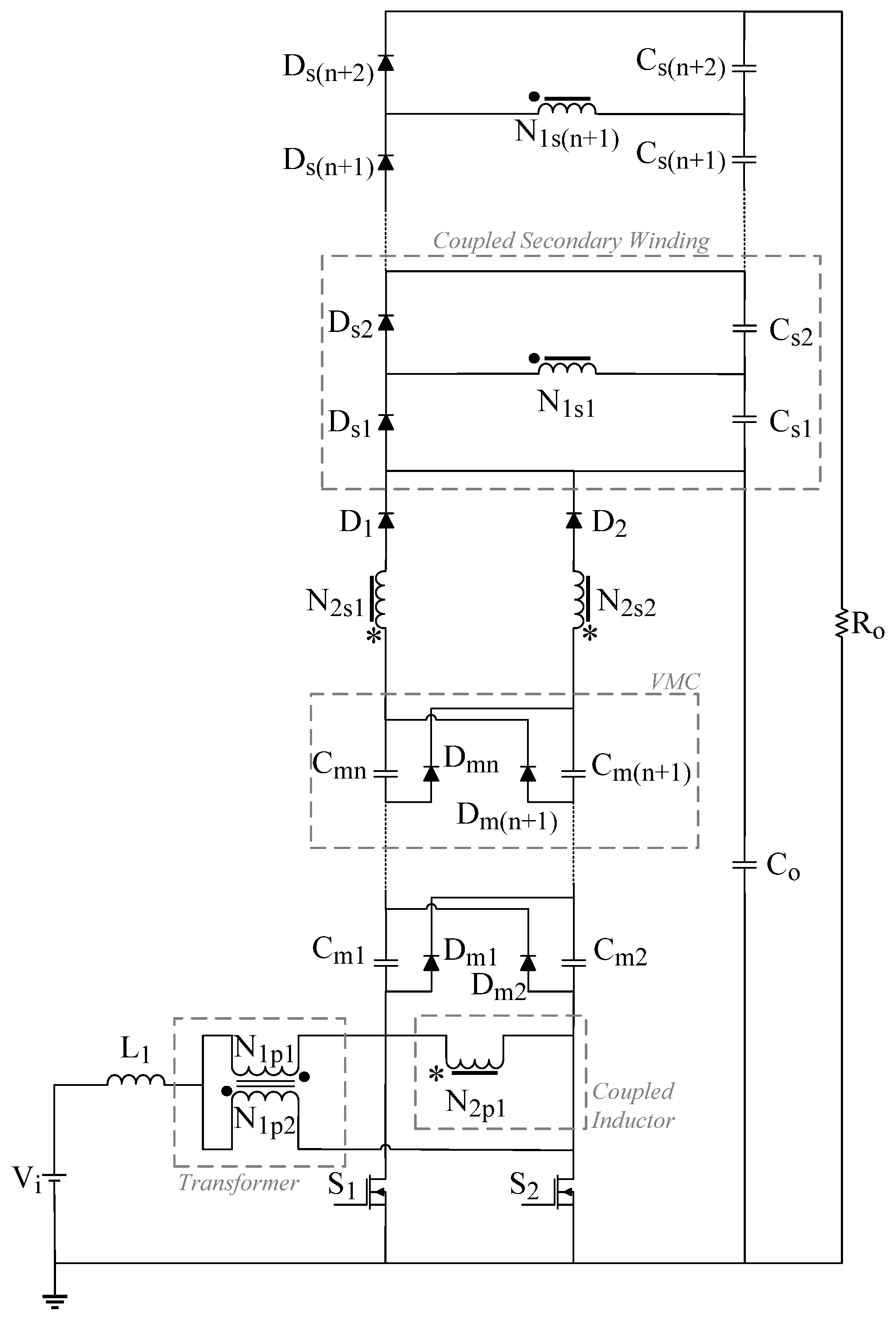
Figure 1. Proposed non-isolated high step-up interleaved boost converter based on a transformer with two interconnected primary windings and multiple secondary windings, VMCs, and a three-winding coupled inductor.
Energies 18 05199 g001
Figure 2. Operating stages of the proposed non-isolated high step-up dc-dc interleaved boost converter in CCM: (a) first stage, (b) second stage, (c) third stage, (d) fourth stage, (e) fifth stage, (f) sixth stage, (g) seventh stage, and (h) eighth stage.
Energies 18 05199 g002aEnergies 18 05199 g002b
Figure 3. Main theoretical waveforms of the proposed non-isolated high step-up dc-dc interleaved boost converter in CCM.
Energies 18 05199 g003
Figure 4. Time domain response of the converter and small-signal model: (a) vo(s)/d(s), (b) vo(s)/iL(s), and (c) iL(s)/d(s).
Energies 18 05199 g004
Figure 5. Voltage gain as a function of the duty cycle.
Energies 18 05199 g005
Figure 6. Normalized voltage stress on the switch as a function of the duty cycle.
Energies 18 05199 g006
Figure 7. Normalized voltage stress on the output diode as a function of the duty cycle.
Energies 18 05199 g007
Figure 8. Experimental prototype of the proposed non-isolated high step-up dc-dc interleaved boost converter.
Energies 18 05199 g008
Figure 9. Output voltage (orange) and output current (green).
Energies 18 05199 g009
Figure 10. Gate-to-source voltage (orange) and input current (green).
Energies 18 05199 g010
Figure 11. Drain-to-source voltages on switches S1 (orange) and S2 (cyan).
Energies 18 05199 g011
Figure 12. Voltages across the transformer windings N1p1 (orange) and N1s1 (cyan).
Energies 18 05199 g012
Figure 13. Anode-to-cathode voltages across diodes D1 (orange) and D2 (cyan).
Energies 18 05199 g013
Figure 14. Anode-to-cathode voltages on diodes Ds1 (orange) and Ds2 (cyan).
Energies 18 05199 g014
Figure 15. Anode-to-cathode voltages on diodes Dm1 (orange) and Dm2 (cyan).
Energies 18 05199 g015
Figure 16. Efficiency as a function of the output power.
Energies 18 05199 g016
Figure 17. Loss breakdown at the rated power condition.
Energies 18 05199 g017
Table 1. Comparison among non-isolated high step-up dc-dc interleaved boost converters based on coupled inductors.
ParameterProposed
Converter
[15][16][17][18][19][20]
Switches2232222
Diodes 2 + 2 m c + 2 N S 475544
Capacitors 1 + 2 m c + 2 N S 374446
Cores3231214
Windings 6 + N S 453436
Gain (Vo/Vi) n 1 + n 2 + m c 1 D 1 1 D + 2 n n 1 + D 1 D n 2 D 1 D 3 n + 1 1 D 1 + n + D 1 D 2 n + D + 1 1 D
VS(max.)/Vo 1 n 1 + n 2 + m c 1 1 + 2 n 2 n D 1 2 n 1 1 2 n 2 D 1 3 n + 1 1 1 + n + D 1 2 n + D + 1
VD(max.)/Vo n 1 n 1 + n 2 + m c n 1 + 2 n 2 n D 1 2 1 2 D 2 n 3 n + 1 1 1 + n + D n + 1 2 n + D + 1
Specifications48 V/400 V24 V/100 V40 V/420 V24 V/200 V40 V/400 V40 V/400 V48 V/800 V
25 kHz50 kHz100 kHz50 kHz50 kHz50 kHz50 kHz
1 kW200 W210 W200 W400 W500 W1 kW
95.12%95.8%96.5%96.2%97%94.5%93%
Common groundYesYesYesNoYesNoYes
ModularityYesNoNoNoNoNoNo
Isolated drive circuitryNoNoNoYesNoYesNo
Improved current sharingYesNoNoNoNoNoNo
Electrolytic capacitorsNoYesYesYesYesYesNo
Table 2. Specifications of the experimental prototype.
ParameterSpecification
Input voltageVi = 48 V
Output voltageVo = 400 V
Rated output powerPo = 1000 W
Switching frequencyfs = 25 kHz
Rated duty cycleD = 0.58
Input filter inductor rippleΔIL1 = 15%·IL1
Voltage ripple across C1, C2, and C3ΔVC = 0.25%·Vo
Voltage ripple across Cm1 and Cm2ΔVCm = 0.5%·Vo
Output voltage rippleΔVo = 0.25%·Vo
Switches S1 and S2MOSFET IRFP90N20 by Infineon
Diodes D1, D2, Ds1, Ds2, Dm1, and Dm2Ultrafast diode U860 by ON Semiconductor
Capacitor C133 μF/250 V polypropylene capacitor
Capacitors C2 and C3Two parallel-connected 33 μF/250 V polypropylene capacitors
Capacitors Cm1 and Cm2Two parallel-connected polypropylene capacitors, rated at 10 μF/250 V and 33 μF/250 V
Filter inductor L1L1 = 50 µF
Core: MMT052T7725 by Magmattec
18 turns, 21 × AWG22
TransformerCore: NEE-65/33/26 by Thornton
N1p1 = N1p2 = 10 turns − 12 × AWG22
N1s1 = 15 turns − 8 × AWG22
(n1 = N1s1/N1p1 = 1.50)
Three-winding coupled inductorCore: NEE-55/28/21 by Thornton
N2p1 = 17 turns − 4 × AWG22
N2s1 = N2s2 = 21 turns − 2 × AWG22
(n2 = N2s1/N2p1 = 1.24)
Table 3. Comparison between calculated and experimentally measured values.
ParameterCalculatedMeasured
Average inductor current (IL1)20.83 A20.90 A
Inductor current ripple (ΔIL1)3.13 A3.11 A
Average output voltage (Vo)400.00 V400 V
Maximum voltage across the switches (VS1(max), VS2(max))114.49 V112 V
Maximum reverse voltage across the output diodes (VD1(max), VD2(max))−133.84 V−148 V
Maximum reverse voltage across the multiplier diodes (VDm1(max), VDm2(max))−228.93 V−224 V
Maximum reverse voltage across the secondary diodes (VDs1(max), VDs2(max))−161.50 V−164 V
Maximum voltage across the multiplier capacitors (VCm1(max), VCm2(max))114.49 V112 V
Maximum voltage across the output filter capacitor (VCo(max))238.68 V246 V
Maximum voltage across the secondary capacitors (VCs1(max), VCs2(max))80.96 V84 V
Maximum voltage on the primary windings of the transformer (VN1p1(max), VN1p2(max))57.24 V56 V
Maximum voltage on the secondary winding of the transformer (VN1p1(max))80.96 V80 V
Maximum voltage on the primary winding of the coupled inductor (VN2p1(max))114.49 V112 V
Maximum voltage on the secondary windings of the coupled inductor (VN221(max), VN2s2(max))124.18 V130 V
Disclaimer/Publisher’s Note: The statements, opinions and data contained in all publications are solely those of the individual author(s) and contributor(s) and not of MDPI and/or the editor(s). MDPI and/or the editor(s) disclaim responsibility for any injury to people or property resulting from any ideas, methods, instructions or products referred to in the content.