Article

State-Set-Optimized Finite Control Set Model Predictive Control for Three-Level Non-Inverting Buck–Boost Converters

1
School of Electrical Engineering, Dalian Jiaotong University, Dalian 116024, China
2
School of Electrical and Automation Engineering, Nanjing Normal University, Nanjing 210023, China
3
School of Optoelectronic Engineering and Instrumentation Science, Dalian University of Technology, Dalian 116024, China
*
Author to whom correspondence should be addressed.
Energies 2025, 18(17), 4481; https://doi.org/10.3390/en18174481
Submission received: 30 July 2025 / Revised: 16 August 2025 / Accepted: 17 August 2025 / Published: 23 August 2025
(This article belongs to the Special Issue Control and Optimization of Power Converters)

Abstract

Three-level non-inverting buck–boost converters are promising for electric vehicle charging stations due to their wide voltage regulation capability and bidirectional power flow. However, the number of three-level operating states is four times that of two-level operating states, and the lack of a unified switching state selection mechanism leads to serious challenges in its application. To address these issues, a finite control set model predictive control (FCS-MPC) strategy is proposed, which can determine the optimal set and select the best switching state from the excessive number of states. Not only does the proposed method achieve fast regulation over a wide voltage range, but it also maintains the input- and output-side capacitor voltage balance simultaneously. A further key advantage is that the number of switching actions in adjacent cycles is minimized. Finally, a hardware-in-the-loop experimental platform is built, and the proposed control method can realize smooth transitions between multiple operation modes without the need for detecting modes. In addition, the state polling range and the number of switching actions are superior to conventional predictive control, which provides an effective solution for high-performance multilevel converter control in energy systems.

1. Introduction

With the advantages of cleanliness, energy saving and high efficiency [1,2], new energy vehicles have gradually become an indispensable mode of transport for people who travel. However, due to the long charging time of conventional electric vehicles and the difference in charging voltage levels of different manufacturers, the voltage fluctuation ranges from 200 V to 920 V [3], and some of them even reach 1000 V [4]. Therefore, the solution of DC/DC fast-charging technology with adaptable high voltage, high power, and wide voltage range has received extensive attention from researchers.
The buck–boost converter has been widely adopted in electric vehicle charging stations, energy storage systems, and DC micro grids due to its non-inverting output and flexible voltage regulation capabilities [5,6]. However, as fast-charging power levels increase from tens of kilowatts to hundreds of kilowatts, there exists an urgent demand for power conversion solutions that support ultra-wide voltage ranges. A novel buck–boost flying capacitor converter for electric vehicle (EV) fast-charging station DC–DC stages has been proposed in [7]. On this basis, an improved DC–DC buck–boost partial power converter with better efficiency compared to [7] is subsequently developed in [8]. However, conventional two-level buck–boost converters with single-leg topology have inherent limitations—switching devices experience increased voltage stress at high output voltages, which raises the susceptibility to overvoltage damage. This operational constraint necessitates the selection of devices with higher voltage class, resulting in increased cost and challenges in increasing the switching frequency. Consequently, existing two-level buck–boost converter architectures are proving inadequate to meet the requirements of high-power, fast-charging systems.
To address the trade-offs between voltage stress and switching frequency, three-level buck–boost topologies have been investigated. These configurations achieve multi-level output characteristics through flying capacitors or cascaded structures [9,10], effectively reducing device voltage stress to 50% of conventional topologies. The three-level framework offers dual advantages: (1) filter size can be reduced, and power density can be improved by multi-level waveform generation, and (2) lower-voltage devices facilitate higher switching frequency operation, thereby enhancing the dynamic response. However, the three-level topology presents significant challenges in implementing control strategies such as multi-mode operation, input/output capacitor voltage balance, and switching state optimization.
In terms of control strategies, conventional two-level buck–boost converters have inherent defects during mode transitions due to minimum pulse width limitation [11]. Specifically, when the input and output voltages approach equilibrium, the voltage gain dead zone in the buck–boost mode transition region occurs in conventional control strategies, resulting in regulation failure [12]. To address this problem, a variety of strategies have been investigated to improve performance. For non-inverting buck–boost topologies, a multi-mode operation strategy has been proposed in [13], where an additional buck–boost mode is introduced alongside the conventional buck and boost modes to mitigate the dead-zone effects. However, this approach can lead to switching oscillations in the region of critical transition thresholds. To suppress such oscillations, a hysteresis control has been implemented in [14].
To further enhance the dynamic characteristics of the converter, the MPC strategy is widely adopted. A modulated MPC is proposed in [15], where the operating state is divided into four modes and the optimal duty cycle is selected via a voltage-based cost function. A key drawback, however, is that this algorithm requires explicit monitoring of the operating mode. To overcome this problem, three operating modes are classified in [16], and the cost function is selected as the minimum fluctuation of inductor current in each control cycle, so that the optimized duty cycle for the subsequent control interval is preferred. For FCS-MPC, a state-space model including switching states is established in [17], and four switching states are polled to optimize the output voltage tracking effect. Since the cost function does not include the inductor current, it is prone to cause current inrush. Building on [17], the work in [18] refines this approach by incorporating both the inductor current and its limit into the cost function. This dual-objective optimization ensures smooth output voltage transitions while effectively suppressing current inrush. Unlike that with two levels, the three-level buck–boost converter confronts the following problems: Firstly, the capacitor voltage balancing control on the input and output sides needs to be regulated. Secondly, the four half-bridge topologies can generate 16 switching states [19], and the global polling computational burden increases dramatically. Finally, the voltage oscillation phenomenon still exists when the input and output voltages are close to each other. To address these issues, Ref. [20] proposes a modulated MPC that introduces two extended operating modes and employs duty cycle hysteresis control to prevent mode oscillations. Notably, the monitor of the converter operating mode is also required, and the optimal number of switching actions cannot be guaranteed. For FCS-MPC, the duty cycle is solved in [21], and the optimal duty cycle is polled in the range of 0 to 1 as a way to achieve optimal control. However, the duty cycle has continuous characteristics, and its accuracy under discrete polling does not meet the demand for control accuracy.
Aiming to address limitations in existing FCS-MPC strategies, a switch-state-optimized FCS-MPC method is proposed in this paper. The contributions can be listed as follows:
(1)
The total number of switching states is reduced from 16 to 11 while retaining full-range buck–boost operation and capacitor voltage balancing capabilities, thereby reducing control complexity. Additionally, the proposed adjacent-state polling strategy further limits candidate states per control cycle to a maximum of five, substantially decreasing computational load and switching losses.
(2)
A multi-objective cost function integrating mode transitions, capacitor voltage balancing, and current tracking is established to enable systematic trade-offs among objectives.
(3)
Seamless mode switching through shared bridging state (M1) ensures smooth transition for different load scenarios.
Ultimately, the proposed control dynamically optimizes switching actions and mode transitions, offering a novel solution for efficient control of three-level topologies. This paper is organized as follows: The principle and discrete state-space model of the three-level buck–boost converter are analyzed in Section 2. The switching state optimization method is proposed in Section 3. Next, the FCS-MPC algorithm is presented in Section 4. Section 5 validates the effectiveness of the proposed method through hardware-in-the-loop. Finally, the conclusions are presented in Section 6.

2. Three-Level Non-Inverting Buck–Boost Converter Working Principle

2.1. Subsection Working Principle of TLNIBBC

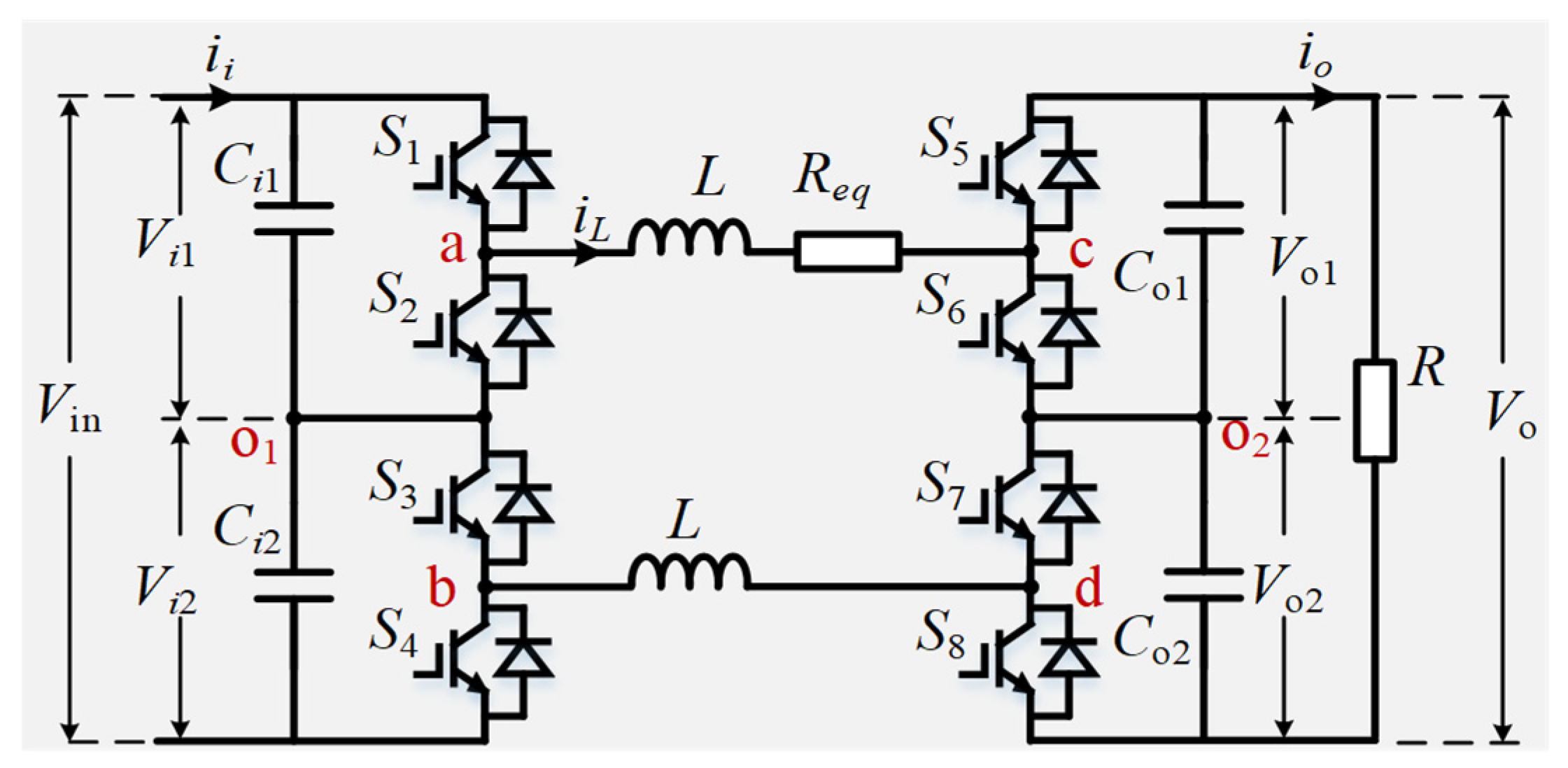
The topology of the three-level non-inverting buck–boost converter is shown in Figure 1. It consists of eight switches named S1S8 and their anti-parallel diodes. Among them, R represents the load resistance and L is the inductor connecting the input and output sides. Req represents the equivalent resistance of the inductor and the loop. Ci1 and Ci2 are the input-side support capacitors with voltages Vi1 and Vi2, respectively, and the sum of which is the total input-side voltage Vin. Similarly, Co1 and Co2 are the output-side capacitors of the converter, with voltages Vo1 and Vo2, respectively, and the sum of which is the total output voltage Vo. In addition, ii and io are the input-side and output-side currents, respectively. Points o1 and o2 are the midpoints of the input and output capacitors. Points a, b, c, and d represent the output terminals of the four half-bridge legs, and the potentials are controlled by switching-state pairs (S1, S2), (S3, S4), (S5, S6), and (S7, S8).
The three-level non-inverting buck–boost converter can be divided into a buck arm on the input side and a boost arm on the output side, of which both sides are symmetrical with respect to the inductance. Both buck and boost arms are cascaded by two half-bridge two-level converters. To avoid short-circuiting of capacitor Ci1, switching states S1 and S2 are complementary. Likewise, the switching states S3 and S4, S5 and S6, and S7 and S8 are each complementary. The three-level non-inverting buck–boost converter can be operated in either buck mode or boost mode.
As seen in Figure 2, the first row (modes ① to ④) forms the boost operating mode, while the first column (modes ①, ⑤, ⑨, and ⑬) constitutes the buck operating mode. Notably, mode ① is a shared state for both buck and boost operations. Therefore, theoretically, only these seven operating states are needed to achieve any step-up or step-down voltage conversion. However, these two operating modes alone cannot guarantee voltage balance across the input-side and output-side capacitors. Hence, additional modes must be incorporated. For instance, controlling the duty cycles of modes ⑦ and ⑪ enables voltage balancing for the input-side capacitors. Similarly, voltage balancing for the output-side capacitors can be achieved by controlling the duty cycles of modes ⑥ and ⑩. In summary, only 11 operating modes are required to implement the buck–boost conversion function.

2.2. Time-Domain State-Space Model

Defining the switching states of the four half-bridges of the three-level non-inverting buck–boost as Q1–Q4, respectively, the following can be obtained:
Q 1 = 1 , S 1 o n a n d S 2 o f f 0 , S 1 o f f a n d S 2 o n     ,         Q 2 = 1 , S 3 o n a n d S 4 o f f 0 , S 3 o f f a n d S 4 o n Q 3 = 1 , S 5 o n a n d S 6 o f f 0 , S 5 o f f a n d S 6 o n     ,         Q 4 = 1 , S 7 o n a n d S 8 o f f 0 , S 7 o f f a n d S 8 o n
According to the KVL equation, the input side midpoint voltage of the arm can be obtained as
v a b = 2 L d i L d t + R e q i L + v c d
Further simplification can be obtained:
v a b = Q 1 V i 1 + ( 1 Q 2 ) V i 2
Similarly, the output side voltage can be obtained as follows:
v c d = Q 3 V o 1 + ( 1 Q 4 ) V o 2
For the input-side capacitance, applying the KCL equation gives
C i 1 d V i 1 d t = i i Q 1 i L C i 2 d V i 2 d t = i i ( 1 Q 2 ) i L
Likewise, the output side can be obtained:
C o 1 d V o 1 d t = Q 3 i L V o 1 + V o 2 R C o 2 d V o 2 d t = ( 1 Q 4 ) i L V o 1 + V o 2 R
Combined with (2) to (6), the time-domain state-space model of a three-level non-inverting buck–boost DC–DC converter can be written in a unified matrix form:
x ˙ = A x + B u
where  x = i L V i 1 V i 2 V o 1 V o 2 T u = i i .
A = R eq 2 L Q 1 2 L ( 1 Q 2 ) 2 L Q 3 2 L ( 1 Q 4 ) 2 L Q 1 C i 1 0 0 0 0 ( 1 Q 2 ) C i 2 0 0 0 0 Q 3 C o 1 0 0 1 R C o 1 1 R C o 1 ( 1 Q 4 ) C o 2 0 0 1 R C o 2 1 R C o 2 ,   B = 0 1 C i 1 1 C i 2 0 0 T
iL represents the inductor current, and Q1Q4 are the switching state variables, which reflect the on–off situation of the switches S1S8. In summary, (7) is applicable whether the converter is in buck mode or boost mode.

2.3. Discrete State-Space Model

Based on the differential equations in the previous section, the continuous time model (7) is discretized by the forward Euler formula, and then the discrete time model of the converter can be obtained:
x p k + 1 = G T s x k + H T s u k
where  G T s = e A T s H T s = 0 T s e A t d t B . Ts is the sampling time. xp(k + 1) is the predicted value of state variable x at time k + 1, where xp = [iLp, Vi1 p, Vi2 p, Vo1 p, Vo2 p]T. Substituting (7) into (8), the inductor current discrete-time model can be written as
i L p k + 1 = 1 R e q T s 2 L i L k + Q 1 T s 2 L V i 1 k Q 3 T s 2 L V o 1 k + 1 Q 2 T s 2 L V i 2 k 1 Q 4 T s 2 L V o 2 k
The discretized equations of the input- and output-side capacitor voltages are written as follows (10)–(13):
V i 1 p k + 1 = Q 1 T s C i 1 i L k + V i 1 k + T s C i 1 i i k
V i 2 p k + 1 = 1 Q 2 T s C i 2 i L k + T s C i 2 i i k + V i 2 k
V o 1 p k + 1 = Q 3 T s C o 1 i L k + 1 T s R C o 1 V o 1 k T s R C o 1 V o 2 k
V o 2 p k + 1 = 1 Q 4 T s C o 2 i L k T s R C o 2 V o 1 k + 1 T s R C o 2 V o 2 k
Equations (9)–(13) are discrete-time state variables, and according to this model, the MPC can be easily implemented.

3. Optimization of Multi-Mode Switching States

The discrete-time model is defined by switching state variables Q1Q4, where each binary variable Qi (i = 1, 2, 3, 4) is constrained to two states (0 or 1). Consequently, 11 distinct mathematical expressions are derived for the discrete-time model. When a conventional MPC algorithm is applied, the discrete state variables must be evaluated 16 times per control cycle, resulting in an excessive computational burden on the controller. More critically, if each switch state is polled exactly according to the inner-loop current prediction, the number of switching actions in the neighboring control cycle is severely increased, and the performance of the converter deteriorates. For instance, a direct transition from the switching state 1010 to 0101 would require all eight switches to be toggled simultaneously, causing significant switching losses that are highly detrimental to converter efficiency. To mitigate these issues, systematic classification and optimization of converter modes are necessitated. The optimization strategies under three operational scenarios—buck mode, boost mode, and transient alternating states—are elaborated in the following sections.

3.1. Switching State Optimization in Buck Mode

The current paths corresponding to the four modes (M1–M4) of the three-level non-inverting converter operating in buck mode are illustrated in Figure 3. In Figure 3a, the switching states of Q1Q4 are configured as 1010, where the load power is supplied jointly by the input voltage source and the inductor. In M2, with switching state 1110, the input capacitor Ci1 and the inductor power the load, causing Ci1 to discharge. Similarly, for the switching state 0110 shown in Figure 3c, the load is supplied by the inductor and supporting capacitors, with both Ci1 and Ci2 being bypassed. Finally, in Figure 3d, state 0010 is activated, enabling the load power to be provided by the input-side capacitor Ci2 and inductor, accompanied by the discharge of Ci2.
The four operational states of the buck mode are systematically concluded in Table 1. It is observed that the switching state transitions between adjacent operational states are characterized by a single-bit variation in the states of Q1Q4. Therefore, in order to suppress the drastic increase in the number of switching actions in the adjacent control cycle of the converter, three alternative states in the next control cycle are polled: one is to keep the state of the previous cycle unchanged, and the other two are to go into the adjacent states. Thus, the schematic of the state transfer in buck mode of the three-level converter is obtained, as shown in Figure 4.
If the current control cycle is in state M1, the range for state optimization in the next control cycle is M1, M2, and M4. As the number of switching actions between M1 and M3 is two, state M3 is excluded in the next cycle. In addition, the decision as to which of the modes, M1, M2, or M4, to select is determined by the cost function described later.

3.2. Switching State Optimization in Boost Mode

The current paths corresponding to the four operational states (M1, M5–M7) of the three-level non-inverting converter in boost mode are illustrated in Figure 5. In Figure 5a, the switching states of Q1Q4 are configured as 1010, where the load power is supplied by both the input source and the inductor. In Figure 5b, the switching states of Q1Q4 are set to 1011. Here, the load power is provided by the output capacitors, while capacitor Co1 is charged and Co2 discharged. As shown in Figure 5c, when the switching states of Q1Q4 are 1001, the load is supplied by supporting capacitors, and energy is stored in both inductors during the state. Finally, in Figure 5d, the switching states of Q1Q4 are 1000. The load power is provided by the supporting capacitors, with capacitor Co2 being charged and Co1 discharged.
Four operational states of the three-level non-inverting converter in boost mode are summarized in Table 2. Similar to the buck mode, only one switching state variation is permitted between adjacent operational states for switching devices Q1Q4. To mitigate excessive switching actions across consecutive control cycles, the candidate states for the next control cycle are restricted to three possibilities: one is to keep the state of the previous cycle unchanged, and the other two are to go into the adjacent states. A schematic representation of the state transition constraints for boost mode is illustrated in Figure 6.
If the current control cycle is in state M1, the range for state optimization in the next control cycle is M1, M5, and M7. As the number of switching actions between M1 and M6 is two, state M6 is excluded in the next cycle. In addition, the decision as to which of the modes, M1, M5, or M7, to select is determined by the cost function described later.

3.3. Transient Switching Process Within Two Operation Modes

The state transition processes of the converter in both buck and boost modes are analyzed separately in the preceding sections. However, in practical applications where the input or output voltage varies over a wide range, transitions between buck and boost modes must be considered. Under such conditions, the transitional process between the two modes termed the bridging mode is required to be addressed.
It is worth noting that state M1 is identified as a common mode shared by both buck and boost operations. Therefore, M1 serves as a critical intermediary bridge for mode transitions. When the converter operates in state M1, five potential operational states—M1, M2, M4, M5, and M7—are permitted in the subsequent control cycle. By leveraging M1 as the bridging state, it is ensured that only one switch variation occurs during transients, thereby effectively suppressing excessive switching actions.

4. The Proposed FCS-MPC

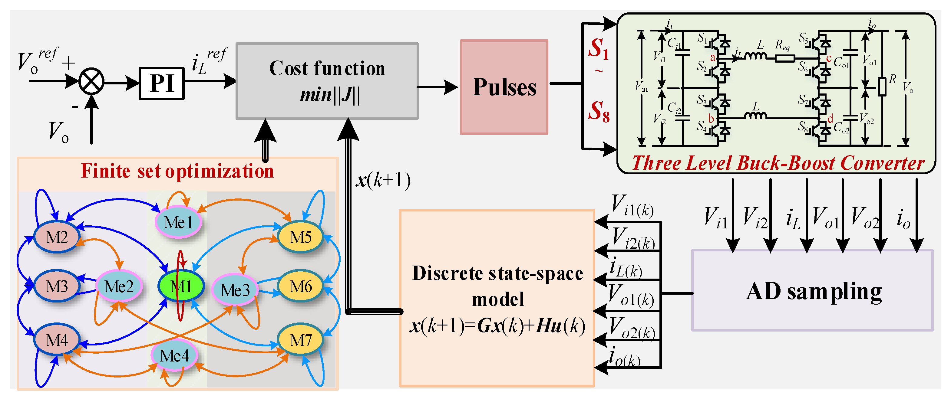
MPC has been widely adopted in power electronics and motor drive systems due to its fast dynamic response, simplified control structure, and straightforward implementation of switching states. For these reasons, the FCS-MPC architecture is adopted in this paper. The block diagram of the proposed FCS-MPC is shown in Figure 7.
The proposed FCS-MPC method is composed of two control loops: a voltage outer loop and a predictive current inner loop. First, the output voltage Vo is sampled and compared with its reference value Vref. The resulting error is processed by a PI controller, thereby generating the reference current iLref for the inner loop. Furthermore, the input capacitor voltage Vin, output capacitor voltage Vo, and inductor current iL are sampled and substituted into the discrete state-space prediction model (8) to derive the predicted state variables. These predicted values, along with their reference values, are incorporated into the cost function. Subsequently, the cost function is evaluated for all candidate switching states using the proposed operational state optimization strategy. The switching state that minimizes the cost function is selected as the optimal solution across the next control cycle. Finally, the corresponding pulse signals are distributed to the switching devices.

4.1. Selection of the Cost Function

As illustrated in Figure 7, the reference current for the inner loop is obtained via the outer-loop voltage PI controller. To ensure accurate tracking of the inductor current, the inductor current is incorporated into the cost function. However, a critical concern arises from the three-level topology: both the input and output voltages are the sum of two capacitor voltages. If the upper and lower capacitor voltages are not actively regulated, voltage unbalance may be induced, leading to capacitor voltage deviation. More critically, such deviation can result in uneven voltage stress across the switching devices, which may ultimately lead to device failure due to overvoltage under severe conditions. Therefore, to effectively balance the capacitor voltages on both the input and output sides, the capacitor voltages should also be included as control objectives in the cost function. Therefore, the cost function can be formulated as follows:
J k = i L r e f i L p k + 1 + λ 1 V o 1 p k + 1 V o 2 p k + 1 + λ 2 V i 1 p k + 1 V i 2 p k + 1 + λ i L _ l i m i t
where λ1 and λ2 are designated as the weighting coefficients for output-side voltage balancing control and input-side voltage balancing control, respectively. The cost function is formulated with four terms: inductor current tracking, output-side voltage balancing, input-side voltage balancing, and inductor current limitation. To address overcurrent issues, λiL_limit is introduced as the weighting coefficient for inductor current protection. Specifically, the inductor current is constrained to prevent excessive values, and thus, λiL_limit is defined as follows:
λ i L _ l i m i t = 0 , i L k + 1 < i L _ max , i L k + 1 i L _ max
where iL_max is defined as the inductor current protection threshold. Once the predicted inductor current exceeds iL_max, the weighting coefficient is set to infinity, thereby ensuring that the corresponding switching states are excluded from consideration. Conversely, when the current below iL_max, the weighting coefficient is assigned as zero, eliminating its impact on the remaining terms of the cost function.

4.2. Switching State Optimization Based on Capacitor Voltage Balance Control

After the cost function is finalized, the switching states for each control cycle are optimized such that the following objectives are achieved:
min J k , s u b j e c t t o M i , i ( 1 , 2 , , 8 )
When the converter operates in buck mode, the switching states are polled and optimized among M1–M4. It is noteworthy that, in buck mode, voltage balancing of the input-side capacitors can be achieved by adjusting the duration of states M2 and M4. However, output-side capacitor voltage unbalance cannot be resolved through modes M1–M4. Therefore, to ensure simultaneous voltage balancing on both input and output sides, four additional modes (Me1–Me4) are introduced. The rules for the additional state introductions should be satisfied:
(1)
Voltage balancing on both input and output sides must be achievable in any selected mode.
(2)
The number of switching actions during transitions between adjacent modes must be minimized.
By adhering to these rules, the four supplementary states are incorporated into the control set, as illustrated in Figure 8.
Similarly, to ensure input-side capacitor voltage balancing in boost mode, the aforementioned four supplementary states (Me1–Me4) are incorporated into it. Consequently, the optimized mode selection diagram in Figure 7 is revised and reoptimized as shown in Figure 9. By evaluating all candidate states through (16), the state that satisfies the predefined conditions is selected as the optimal solution for the subsequent control cycle. Notably, out of the total 16 possible switching states, only 11 states are utilized in the proposed control strategy, with the remaining 5 states excluded from consideration.
Since only one switching state variation is permitted between consecutive control cycles, the subsequent candidate states are restricted to M1, M2, M3, Me1, and Me2 when the current state is M2 and input voltage unbalance occurs. If voltage deviation dominates the cost function, the converter may oscillate among M2, M3, and Me2, failing to reach M4 and causing optimization failure. To ensure effective optimization, mode M4 is forcibly included in the candidate set when the converter operates in M2 at moment k. If mode M4 is determined as the optimal state for moment k + 1 via cost function evaluation, mode M1 is temporarily applied at moment k + 1, enabling a feasible transition to M4 at moment k + 2 while maintaining the single switch variation constraint. This strategy prevents optimization failure while ensuring minimal switching actions. A similar approach is adopted for modes M5 and M7.
Therefore, switching transitions are strictly confined to adjacent modes, significantly reducing the computational overhead of state polling and suppressing unnecessary switching state changes.

4.3. Optimal Control Algorithm for Three-Level Non-Inverting Buck–Boost Converter

To elaborate on the proposed MPC algorithm, the procedural flowchart of the control strategy is illustrated in Figure 10. The steps of the FCS-MPC are detailed as follows:
First, the previous switching state Mi(k) is analyzed, and the cost function is initialized with Jopt = ∞. Subsequently, the input voltage, output voltage, and inductor current of the buck–boost converter are sampled. Based on the state transition diagram in Figure 9, the candidate switching states for the current control cycle are identified, and the total number of candidate modes is denoted as N. The indices of all candidate states are stored in an array order [N]. Following this, the cost function values for all N candidate states are computed using (14). If the candidate cost function value Jj is found to be less than Jopt, Jj is assigned to Jopt, and the index j is recorded. After all N states are polled, the j-th state is selected as the optimal state for the next control cycle, and the corresponding eight switching pulse signals are generated. Finally, the switching devices are driven via the gate driver circuit.
The aforementioned process is repeated for each control cycle, iteratively determining the optimal state while minimizing computational overhead and switching transients.
5. Experimental Validation

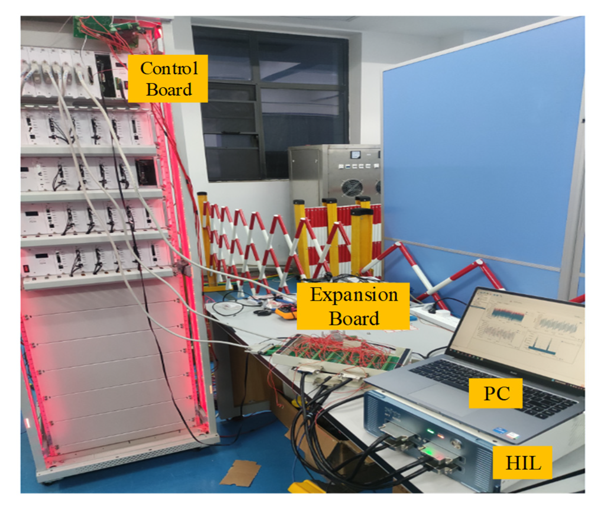
To validate the effectiveness of the FCS-MPC algorithm for three-level non-inverting buck–boost converters, an experimental platform based on the Starsim HIL (Hardware-in-the-Loop) system was constructed in the laboratory. As shown in Figure 11, the digital controller configuration employed a dual-core architecture comprising DSP and FPGA. The Texas Instruments (TI) C2000-series TMS320C28346 DSP is implemented for voltage/current sampling at converter terminals and execution of the FCS-MPC algorithm. The FPGA is utilized for multi-channel pulse processing, including pulse coordination and dead-time configuration. The principles for parameter design of the main circuit can be obtained in [10]. The main parameters of the experiment are summarized in Table 3.
The effectiveness of the proposed control strategy is validated through a series of experimental verifications under the following operating scenarios: buck mode, near-unity voltage ratio conversion, boost mode, input-side voltage balancing, output-side voltage balancing, and wide-range voltage dynamic performance.

5.1. Buck Mode Verification

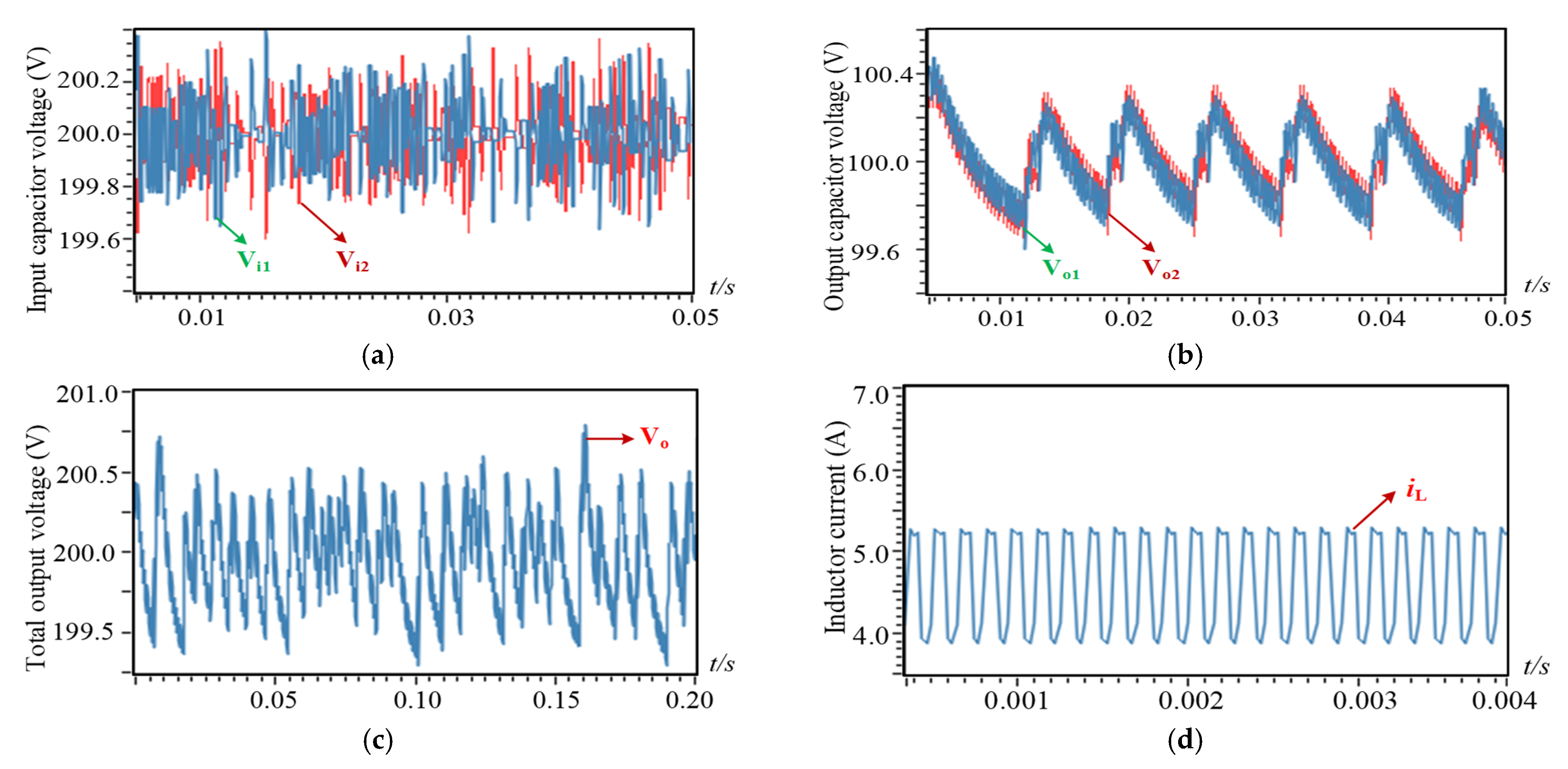
The waveforms of the three-level non-inverting buck–boost converter in buck mode are shown in Figure 12a–d, which corresponding to the input capacitor voltages, output capacitor voltages, total output voltage and inductor current, respectively. As shown in Figure 12a, the voltage fluctuations of the upper and lower input capacitors are maintained between 199.6 V and 200.4 V, demonstrating the effectiveness of the input-side voltage balancing control. The output capacitor voltages shown in Figure 12b are maintained within 99.6 V to 100.4 V, confirming effective voltage balancing at the output side. In addition, the total output voltage shown in Figure 12c is stabilized at 200 V with little fluctuation. In particular, the bridge inductor current shown in Figure 12d is smooth with no apparent current spikes. Therefore, the buck mode experimental results demonstrate that the proposed FCS-MPC strategy achieves effective step-down operation while ensuring balanced voltage control on both input and output capacitors.

5.2. Close Input and Output Voltages

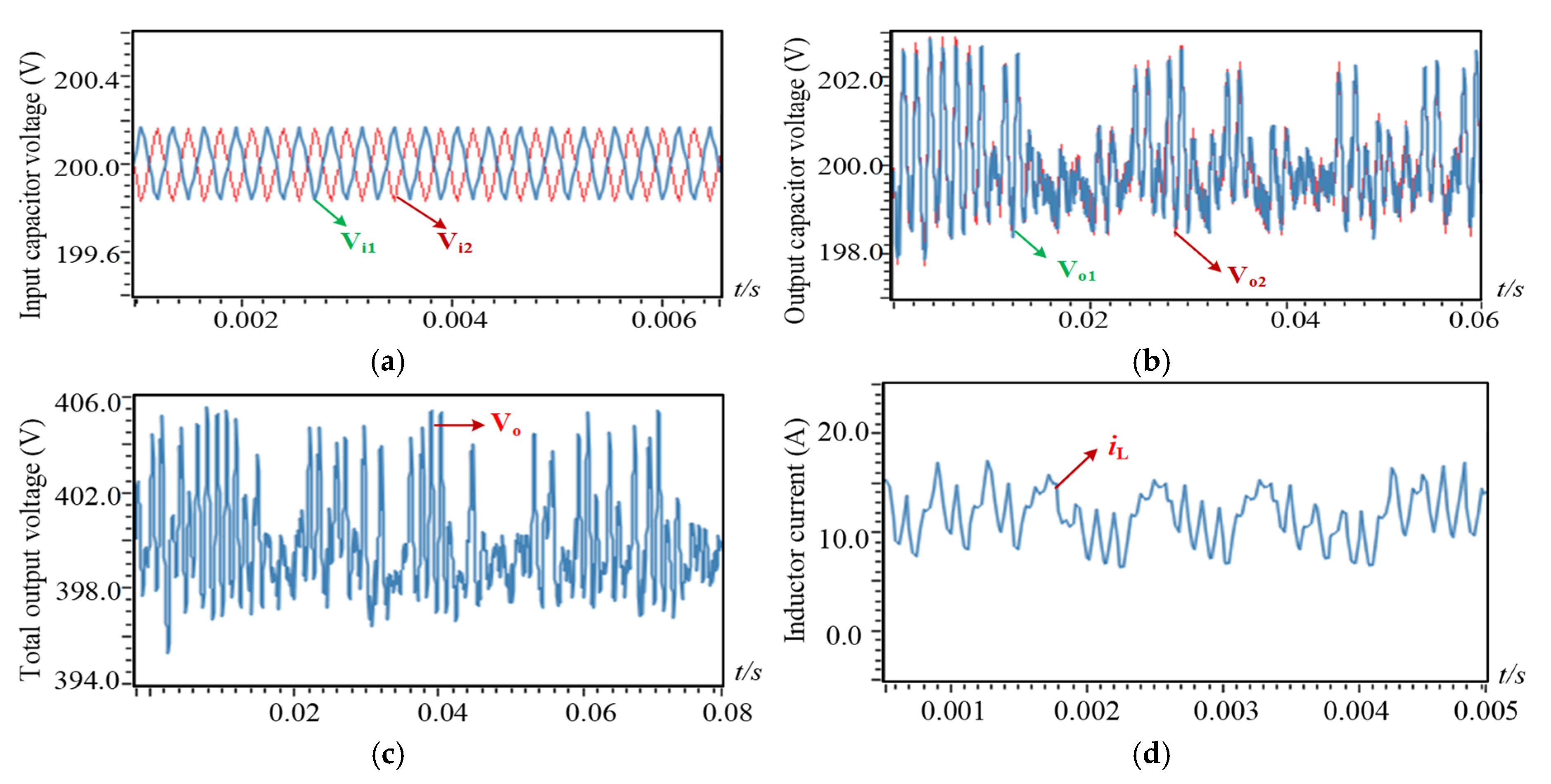
The voltage regulation characteristics of the three-level non-inverting buck–boost converter under near unity voltage ratio operation are shown in Figure 13a–d. As seen in Figure 13a, the upper and lower input capacitor voltages are maintained between 199.8 V and 200.2 V, indicating the effectiveness of voltage balancing at the input-side capacitors. The output capacitor voltages presented in Figure 13b are stabilized around 200 V, with the fluctuations maintained between 198 V and 203 V, confirming effective voltage balancing at the output side. In addition, the total output voltage, shown in Figure 13c, is regulated at 400 V with accurate steady-state operation. In particular, the inductor current shown in Figure 13d demonstrates smooth operation with no apparent current spikes. These experimental results confirm that the proposed FCS-MPC strategy effectively achieves output voltage regulation and bilateral capacitor voltage balancing when input and output voltages approach approximate magnitudes.

5.3. Boost Mode Verification

The waveforms of the three-level buck–boost converter in boost mode are shown in Figure 14a–d. As shown in Figure 14a, the input capacitor voltages are maintained between 199.4 V and 200.6 V, indicating effective voltage balancing between the upper and lower capacitors. The output capacitor voltages shown in Figure 14b are stabilized near 400 V, with fluctuations regulated between 398.0 V and 402.0 V, confirming voltage balancing at the output stage. In addition, the total output voltage shown in Figure 14c is maintained at 800 V with little voltage ripple. Notably, the inductor current shown in Figure 14d exhibits a smooth dynamic behavior without abrupt spikes. These results confirm that the proposed FCS-MPC strategy is capable of achieving boost mode operation, while ensuring balanced voltage regulation across both input and output capacitors.

5.4. Dynamic Processes

(1)
Wide Voltage Range Variation
To validate the smooth control functionality of the three-level buck–boost converter for wide-range output applications, a dynamic experimental verification is conducted by linearly increasing the output reference voltage from 200 V to 800 V, with corresponding experimental waveforms provided in Figure 15a. As revealed in the results, the output voltage achieves smooth transition during the transient process from 200 V to 800 V. Furthermore, the dynamic capacitor voltage balance is maintained between input and output sides throughout the entire operation, demonstrating superior voltage equalization performance. In addition, no significant current surges are detected in the inductor current during the transient process, confirming the effectiveness of the proposed control strategy.
In Figure 15b, the output voltage remains stable at 400 V under a wide range of input voltages from 200 V to 800 V. During the input voltage increase process, the upper and lower capacitor voltages on the input side remain balanced. As the input voltage increases and the load power remains unchanged, the inductor current decreases. In addition, the output voltage remains stable at 400 V, and the upper and lower capacitor voltages of the output-side capacitor are balanced.
(2)
Load Variation
The voltage and current waveforms on the input and output sides under load changes are shown in Figure 16a–d. At t = 0.399 s, the output side load resistance changes from 100 Ω to 50 Ω. Obviously, the inductor current increases instantaneously after the resistance changes. In addition, even though there are transient fluctuations in the input and output voltages, the balance of the capacitor voltages on the input and output sides can still be achieved. The waveform of the total output voltage is shown in Figure 16c. At the moment of load change, the output voltage drops shortly and then quickly stabilizes at 400 V. The inductor current is shown in Figure 16d. At the moment of transient switching, the inductor current increases and gradually goes stable. Therefore, the adaptability to dynamic load fluctuations is validated under the proposed control.

5.5. Statistics on the Number of Switching Actions

(1)
Pulse Signals of Each Device in the Conventional Global Polling Strategy
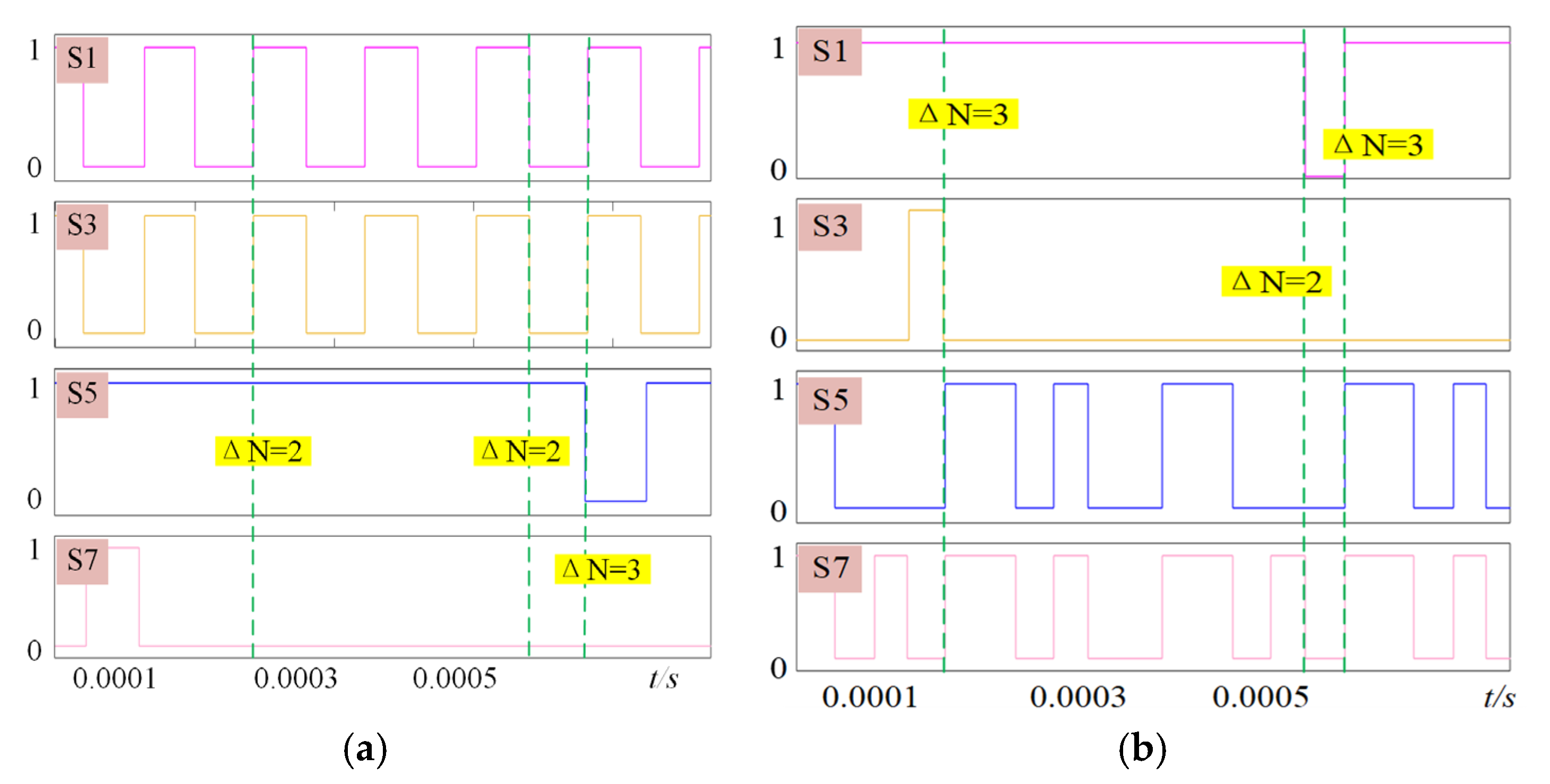
As shown in Figure 17a, the pulse signals of switches S1–S7 are presented under the conventional global polling strategy in buck mode. Notice that the switching action count ΔN between adjacent control intervals is either 2 or 3. Similarly, the corresponding pulse signals in boost mode are shown in Figure 17b, where ΔN likewise falls within {2, 3}. Therefore, under the global polling strategy, multiple devices switching simultaneously are observed during individual control cycles.
(2)
Pulse Signals of Each Device in the Proposed Control Strategy
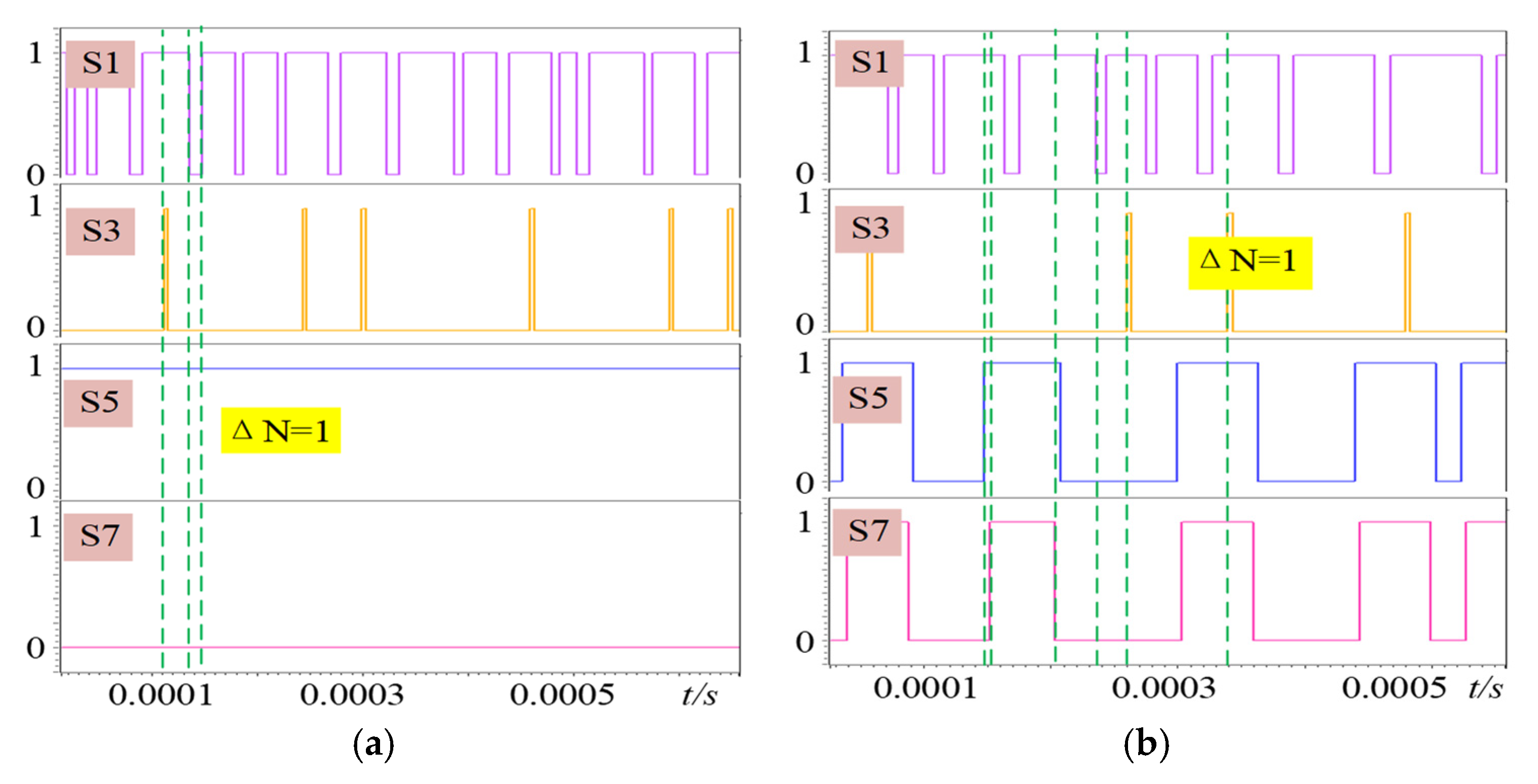
In the buck mode, the pulse signals S1–S7 of the proposed control strategies are shown in Figure 18a. The number of switching actions between two adjacent cycles is ΔN = 1. Therefore, there is only one switching action in each control cycle. Similarly, the pulse signals in the boost mode are shown in Figure 18b, and the characteristic of ΔN = 1 can also be obtained. Therefore, the feasibility of the proposed control strategy to reduce the number of switching actions is verified.
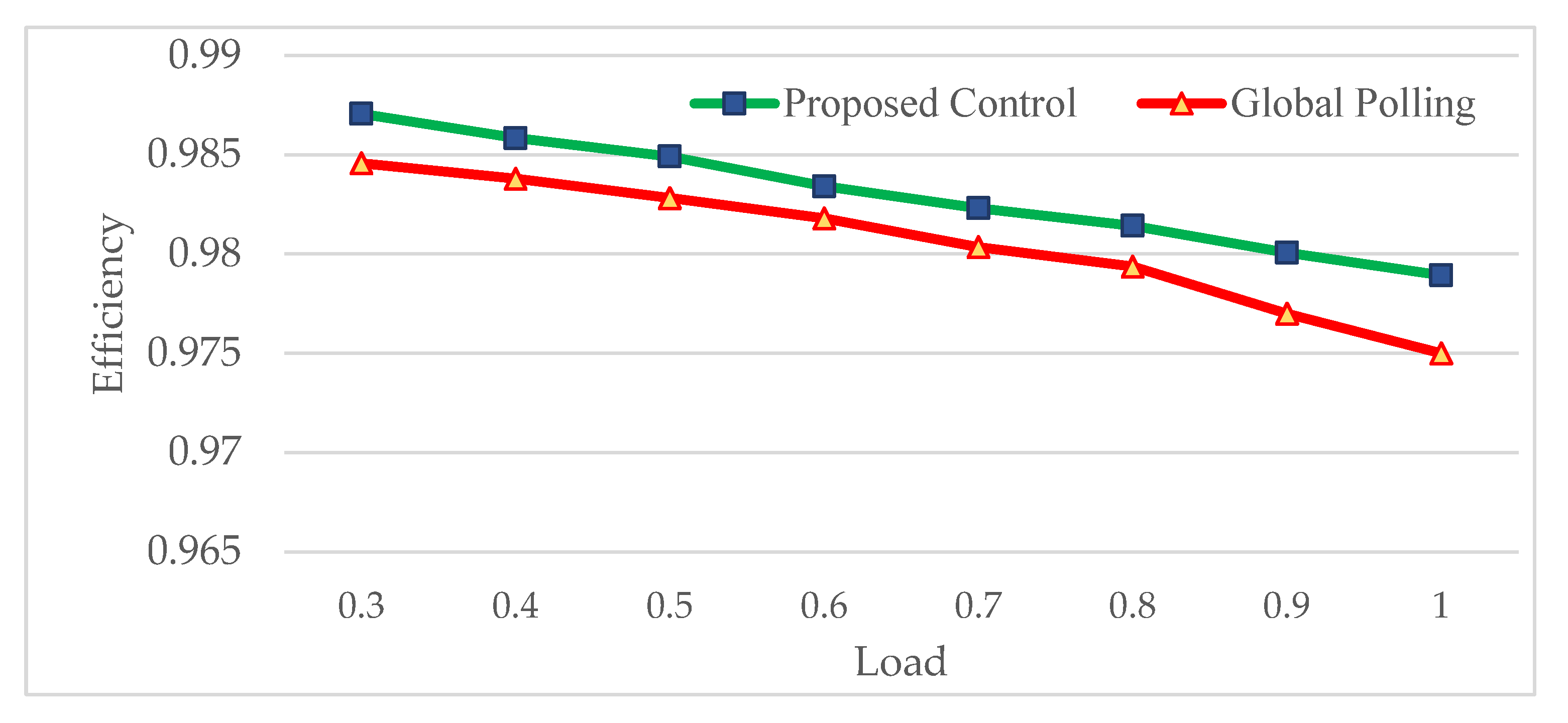
The efficiency under the proposed FCS-MPC and global polling control is shown in Figure 19. It is clear that the efficiency of the system under the proposed FCS-MPC is always higher than that under the global polling strategy, which demonstrates that the proposed control has remarkable advantages in terms of efficiency improvement.

6. Conclusions

An FCS-MPC strategy was proposed for three-level non-inverting buck–boost converters, achieving seamless wide-range voltage regulation through optimized switching action reduction and strategic integration of voltage balancing. By incorporating capacitor voltage equilibrium constraints into the cost function, consistent voltage balancing on both sides was ensured without additional operational mode detection. Experimental results confirm that the proposed strategy provides superior dynamic performance under wide input/output voltage variations and load changes, while maintaining a balanced voltage across the input and output capacitors. Furthermore, switching losses can be significantly reduced and efficiency of the converter improved by minimizing the number of device actions between adjacent control intervals.

Author Contributions

Conceptualization, M.X. and H.D.; methodology, M.X.; validation, R.H., M.X., and H.D.; formal analysis, M.X. and J.T.; investigation, Y.L. and Z.L.; resources, M.X. and X.W.; writing—original draft preparation, M.X.; writing—review and editing, R.H., J.T., and Y.L.; super vision, M.X. and H.D.; project administration, M.X., R.H., and X.W. All authors have read and agreed to the published version of the manuscript.

Funding

This research was funded by the Fundamental Research Funds for the Provincial Universities of Liaoning, grant number LJ212410150040, and the Natural Science Foundation of Liaoning Province, grant number 2025-BS-0448, and the Liaoning Province Transportation Science and Technology Project, grant number 2024066.

Data Availability Statement

The original contributions presented in the study are included in the article, further inquiries can be directed to the corresponding author.

Conflicts of Interest

The authors declare no conflicts of interest.

References

  1. Yuan, J.; Dorn-Gomba, L.; Callegaro, A.D.; Reimers, J.; Emadi, A. A Review of Bidirectional On-Board Chargers for Electric Vehicles. IEEE Access 2021, 9, 51501–51518. [Google Scholar] [CrossRef]
  2. Wouters, H.; Martinez, W. Bidirectional Onboard Chargers for Electric Vehicles: State-of-the-Art and Future Trends. IEEE Trans. Power Electron. 2024, 39, 693–716. [Google Scholar] [CrossRef]
  3. Adnan, A.; Qin, Z.; Wijekoon, T.; Bauer, P. An Overview on Medium Voltage Grid Integration of Ultra-Fast Charging Stations: Current Status and Future Trends. IEEE Open J. Ind. Electron. Soc. 2022, 3, 420–447. [Google Scholar] [CrossRef]
  4. Available online: https://insidechinaauto.com/2025/03/24/byd-announces-first-megawatt-fast-charging-ev-platform/ (accessed on 24 March 2025).
  5. Sharida, A.; Bayhan, S.; Abu-Rub, H. Novel Multi-Mode DC-DC Converter for Battery Storage Applications. In Proceedings of the IECON 2023-49th Annual Conference of the IEEE Industrial Electronics Society, Singapore, 16–19 October 2023. [Google Scholar] [CrossRef]
  6. Kitazoe, K.; Natori, K.; Sato, Y. Bidirectional Power Flow Control Using Four-Switch Buck-Boost Converter in DC Power Network. IEEE J. Ind. Appl. 2024, 13, 618–624. [Google Scholar] [CrossRef]
  7. Pesantez, D.; Rodriguez, F.; Renaudineau, H.; Rivera, S.; Kouro, S. Buck-Boost Flying Capacitor DC-DC Converter for Electric Vehicle Charging Stations. In Proceedings of the 2023 IEEE 17th International Conference on Compatibility, Power Electronics and Power Engineering, Tallinn, Estonia, 14–16 June 2023. [Google Scholar] [CrossRef]
  8. Muñoz, R.V.; Renaudineau, H.; Rivera, S.; Kouro, S. Evaluation of DC-DC buck-boost partial power converters for EV fast charging application. In Proceedings of the IECON 2021–47th Annual Conference of the IEEE Industrial Electronics Society, Toronto, ON, Canada, 13–16 October 2021. [Google Scholar] [CrossRef]
  9. Eull, M.; Preindl, M. Bidirectional three-level DC-DC converters: Sum-difference modeling and control. In Proceedings of the 2017 IEEE Transportation Electrification Conference and Expo, Chicago, IL, USA, 22–24 June 2017. [Google Scholar] [CrossRef]
  10. Bi, K.; Xu, C.; Ai, J.; Li, J.; Fan, Q. Decoupling Model Predictive Controlled Three-Level Noninverting Buck–Boost Converter Applied in DC Energy Storage System. IEEE Trans. Power Electron. 2024, 39, 6677–6687. [Google Scholar] [CrossRef]
  11. Sun, B.; Trintis, I.; Munk-Nielsen, S.; Guerrero, J.M. Effects and analysis of minimum pulse width limitation on adaptive DC voltage control of grid converters. In Proceedings of the 2016 IEEE Applied Power Electronics Conference and Exposition, Long Beach, CA, USA, 20–24 March 2016. [Google Scholar] [CrossRef]
  12. Jia, P.; Hao, Y. Research on the Dead-Time Control Scheme for the Four-Switch Buck-Boost Converter. In Proceedings of the 2020 IEEE 9th International Power Electronics and Motion Control Conference, Nanjing, China, 29 November–2 December 2020. [Google Scholar] [CrossRef]
  13. Jia, L.; Sun, X.; Zheng, Z.; Ma, X.; Dai, L. Multimode Smooth Switching Strategy for Eliminating the Operational Dead Zone in Noninverting Buck–Boost Converter. IEEE Trans. Power Electron. 2020, 35, 3106–3113. [Google Scholar] [CrossRef]
  14. Cao, E.; Ding, W.; Duan, B.; Song, J.; Zhan, C.; Wan, D. Predictive Control Strategy for Four-switch Buck-Boost Converter with Mode Smooth Transition. In Proceedings of the 2022 6th CAA International Conference on Vehicular Control and Intelligence, Nanjing, China, 28–30 October 2022. [Google Scholar] [CrossRef]
  15. Wu, Y.; Wang, W.; Zeng, G.; Wu, X.; Tang, F. Multi-Mode Model Predictive Control Strategy for the Four-Switch Buck-Boost Converter. Trans. China Electrotech. Soc. 2022, 37, 2572–2583. [Google Scholar] [CrossRef]
  16. Bai, Y.; Hu, S.; Yang, Z.; Zhu, Z.; Zhang, Y. Model Predictive Control for Four-Switch Buck–Boost Converter Based on Tuning-Free Cost Function with Smooth Mode Transition. IEEE J. Emerg. Sel. Top. Power Electron. 2022, 10, 6607–6618. [Google Scholar] [CrossRef]
  17. Ullah, B.; Ullah, H. Finite Control Set Model Predictive Control of Noninverting Buck-Boost DC-DC Converter. In Proceedings of the 2022 International Conference on Technology and Policy in Energy and Electric Power, Jakarta, Indonesia, 18–20 October 2022. [Google Scholar] [CrossRef]
  18. Li, X.; Liu, Y.; Xue, Y. Four-Switch Buck–Boost Converter Based on Model Predictive Control with Smooth Mode Transition Capability. IEEE Trans. Ind. Electron. 2021, 68, 9058–9069. [Google Scholar] [CrossRef]
  19. Zhu, Z.; Ma, F.; Lin, L.; Wang, L.; Kuang, D.; Xu, Q. Multimode Smooth Transition Technique for Three-Level Cascaded Noninverting Buck–Boost DC–DC Converter. IEEE Trans. Power Electron. 2021, 36, 14409–14419. [Google Scholar] [CrossRef]
  20. Peng, Q.; Zhou, S.; Ma, F.; Huang, G.; Fan, R. A Model Predictive Control of Three-Level Cascaded Noninverting Buck–Boost Converter for Energy Storage System. IEEE Trans. Ind. Electron. 2025, 72, 4933–4942. [Google Scholar] [CrossRef]
  21. Jayan, V.; Ghias, A.; Merabet, A. Fixed Frequency Model Predictive Control of Three-level Bi-directional Flying Capacitor DC-DC converter in DC microgrid. In Proceedings of the IECON 2019-45th Annual Conference of the IEEE Industrial Electronics Society, Lisbon, Portugal, 14–17 October 2019. [Google Scholar] [CrossRef]
Figure 1. The topology of three-level buck–boost converter.
Energies 18 04481 g001
Figure 2. Summary of operating modes for the three-level buck–boost converter.
Energies 18 04481 g002
Figure 3. Four operation states of buck mode.
Energies 18 04481 g003
Figure 4. Schematic diagram of states transfers in buck mode.
Energies 18 04481 g004
Figure 5. Four operation states of boost mode.
Energies 18 04481 g005
Figure 6. Schematic diagram of state transfers in boost mode.
Energies 18 04481 g006
Figure 7. Block diagram of the proposed FCS-MPC.
Energies 18 04481 g007
Figure 8. Voltage balance states in buck mode and boost mode.
Energies 18 04481 g008
Figure 9. Schematic diagram of state transfer considering capacitor voltage balance on both sides.
Energies 18 04481 g009
Figure 10. Flow chart of the proposed FCS-MPC.
Energies 18 04481 g010
Figure 11. Photograph of experimental platform.
Energies 18 04481 g011
Figure 12. Three-level converter operating in buck mode: (a) voltage of the upper and lower capacitors on the input side; (b) voltage of the upper and lower capacitors on the output side; (c) total output voltage; (d) inductor current.
Energies 18 04481 g012
Figure 13. The waveforms of the three-level converter when the input and output voltages are equal: (a) voltage of the upper and lower capacitors on the input side; (b) voltage of the upper and lower capacitors on the output side; (c) total output voltage; (d) inductor current.
Energies 18 04481 g013
Figure 14. Three-level converter operating in boost mode: (a) voltage of the upper and lower capacitors on the input side; (b) voltage of the upper and lower capacitors on the output side; (c) total output voltage; (d) inductor current.
Energies 18 04481 g014
Figure 15. Dynamic process: (a) wide-range output voltage; (b) wide-range input voltage.
Energies 18 04481 g015
Figure 16. Voltage and current under load changes: (a) upper and lower capacitor voltages on the input side; (b) upper and lower capacitor voltages on the output side; (c) total output voltage; (d) inductance current.
Energies 18 04481 g016
Figure 17. Pulse signals under the global polling strategy: (a) buck mode; (b) boost mode.
Energies 18 04481 g017
Figure 18. Pulse signals under the proposed control: (a) buck mode; (b) boost mode.
Energies 18 04481 g018
Figure 19. The efficiency comparison of converters under different control strategies.
Energies 18 04481 g019
Table 1. Switch states and port voltage in buck mode.
Operation StatesQ1Q2Q3Q4vabvcd
M11010VinVo
M21110Vi1Vo
M301100Vo
M40010Vi2Vo
Table 2. Switch states and port voltage of boost mode.
Operation StatesQ1Q2Q3Q4vabvcd
M11010VinVo
M51011VinVo1
M61001Vin0
M71000VinVo2
Table 3. Parameters of three level buck–boost converter.
ParametersValues
Input Voltage/V400
Output Voltage/V200~800
Inductor/mH0.5
Input-Side Capacitor Ci/mF1.0
Output-Side Capacitor Co/mF1.0
Equivalent resistance Req0.001
Load R/Ω50
Sampling Frequency f/kHz100.0
Control Period Ts/us25.0
Disclaimer/Publisher’s Note: The statements, opinions and data contained in all publications are solely those of the individual author(s) and contributor(s) and not of MDPI and/or the editor(s). MDPI and/or the editor(s) disclaim responsibility for any injury to people or property resulting from any ideas, methods, instructions or products referred to in the content.