1. Introduction
With the rapid developments in semiconductor lighting, light-emitting diodes (LEDs) have been extensively applied to lighting equipment and consumer electronic products because of their high luminous efficiency, pollution-free characteristics, and super longevity [
1,
2]. To achieve sufficient lumens in the aforementioned applications, LEDs are coupled in series and parallel [
3]. This configuration yields the requirement of multi-output constant current for LED drivers. It also requires power factor correction (PFC) and electrical isolation to satisfy power quality standards and safety regulations [
4,
5].
At the present time, approaches for realizing multi-channel constant-current output can be broadly categorized into single-converter and multi-converter schemes [
6]. The multi-converter approach, wherein each LED load is driven by a dedicated DC/DC converter, offers flexible control but is often compromised by high system cost, volume, and complexity [
7]. Consequently, single-converter multiple-output topologies have been extensively investigated. A key technical challenge for these topologies lies in achieving inherent current balancing among the parallel output branches.
As seen in
Figure 1, this two-stage LED driver represents a common option for medium- to high-power applications. PFC converters make up the first stage, and DC/DC converters make up the second stage. Boost, buck, or other converters are often adopted in the first stage to obtain a high power factor and constant output voltage [
8,
9,
10,
11]. To address this challenge, this paper focuses on constant-current control multi-output DC/DC LED drivers [
12,
13] and aims to develop low-cost, high-power density, and high-efficiency solutions [
14].
Among existing single-converter multiple-output current-balancing techniques, passive methods, such as those employing resistors or capacitors, feature a simple structure but suffer from poor regulation accuracy and introduce additional power losses [
15]. In contrast, active methods, while capable of enhancing accuracy by monitoring and controlling each output channel, necessitate complex control circuitry and a significant increase in component count [
16]. In recent years, advanced topologies based on resonant converters, single-inductor multiple-output (SIMO) structures, and electrolytic capacitor-less designs have been successively proposed, effectively enhancing system performance [
17,
18,
19,
20]. In particular, schemes that utilize the constant-current characteristics of resonant networks, such as the LCL-T topology, to establish a high-frequency AC bus have demonstrated considerable potential for multi-load applications [
21].
Despite some progress in recent years, developing solutions that achieve high-precision current sharing, require minimal components, and feature simple control schemes remains a major challenge. This paper addresses these issues by proposing a novel multi-channel LED driver based on a high-frequency AC bus. The driver employs an innovative series rectifier architecture to achieve inherent current sharing.
A current-sharing scheme of a resonant network is proposed in [
21]. Due to the LCL-T constant-current properties, the rectifiers can be designed to function similarly to current sources. In order to provide multiple constant-current outputs, multiple LCL-T rectifiers are coupled to the same high-frequency AC voltage bus. In order to simplify the circuit, increase power density, and reduce costs, more components should be shared among different outputs. The port for the output of the LCL-T passive resonant network can be used to build a high-frequency AC bus in accordance with the circuit duality concept. Each output can also share the passive resonant network apart from the original full-bridge inverter and high-frequency isolation transformer. Thus, as seen in
Figure 2, the constant-current multi-output LED driver constructed using a high-frequency AC bus can be built. The focus of this paper is the second-stage DC/DC converter, whose input,
Udc, is provided by a front-end PFC circuit.
Figure 2 shows the detailed topology of the proposed DC/DC converter part.
Compared to [
21], there are significantly fewer resonant networks, and the circuit structure is significantly simpler. Each string is connected in series before the diode rectifier, so only one output string needs to be sampled and closed-loop controlled. Other output currents can be automatically kept constant since all the strings are driven by the same AC bus. Obviously, high current accuracy can be achieved for multiple LED strings within the change of input and output.
However, for multi-output resonant converters, their stability is of crucial importance. Due to the nonlinear dynamic characteristics of the resonant converter, it is necessary to conduct stability analyses under various working conditions to ensure its stable operation under all conditions. If a linearized system is required, small-signal modeling is indispensable. This method is conducive to the rapid design of an ideal feedback controller [
22]. For modern lighting systems, well-designed controllers must achieve high stability, rapid current regulation, provide fast transient response, and—at the same time—prevent current overtones that may damage LED [
23]
This paper is organized as follows.
Section 2 introduces the proposed DC-fed multi-channel constant-current LED driver.
Section 3 elaborates on the parameter design process and provides a comparative stability analysis for the optimization of the PI controller.
Section 4 details the implementation of the DC/DC control circuitry and verifies its functionality through experimental results. Finally,
Section 5 concludes the paper.
2. The Proposed LED Driver
The topological structure proposed in this paper is an advancement upon and optimization of existing research. The modular topological structure proposed in reference [
21] lays the key foundation for this study. This scheme utilizes the constant-current characteristics of the LCL-T network to drive the LED loads in each channel by connecting multiple LCL-T passive resonant rectifier units in parallel to the high-frequency AC voltage bus. This solution provides ideas for further optimization. Specifically, in this solution, each output channel is equipped with a dedicated LCL-T resonator. Therefore, this solution will inevitably increase the total number of components, cost, and physical volume, thereby limiting the power density.
To address the limitations of the aforesaid schemes, this letter presents a topology with a higher degree of integration, the core principle of which is to consolidate multiple resonant units into a centralized resonant network. This architecture utilizes the constant-current characteristics of an LCL-T network to establish a high-frequency AC bus, to which the rectifier bridges of each output channel are connected in series. This series configuration ensures that the output current of each channel is identical, thereby achieving inherent high-precision current balancing. Simultaneously, this approach significantly reduces the component count of passive elements. The final proposed scheme, derived from the analysis of this topology, is depicted in
Figure 2.
The DC/AC inverter and the LCL-T passive resonant rectifier are the two components of the proposed DC-provided multi-output constant-current LED driver shown in
Figure 2. One LCL-T passive resonant network comes after the DC/AC inverter. After isolation by a transformer, a high-frequency AC bus is formed. Each output string is connected in series with the AC bus through the diode rectifier. Thus, multiple constant-current outputs can be realized with high current accuracy.
Consisting of switches S
1 through S
4, the DC/AC inverter transforms DC electricity into high-frequency AC square voltage. Additionally,
Figure 1 shows the output voltage of the first PFC stage, which is the input DC voltage
Udc. An isolation transformer, T, a diode rectifier linked in series with the LED loads, a DC blocking capacitor,
Cb, and resonant networks
L1,
C1, and
La1 make up the LCL-T passive resonant rectifier.
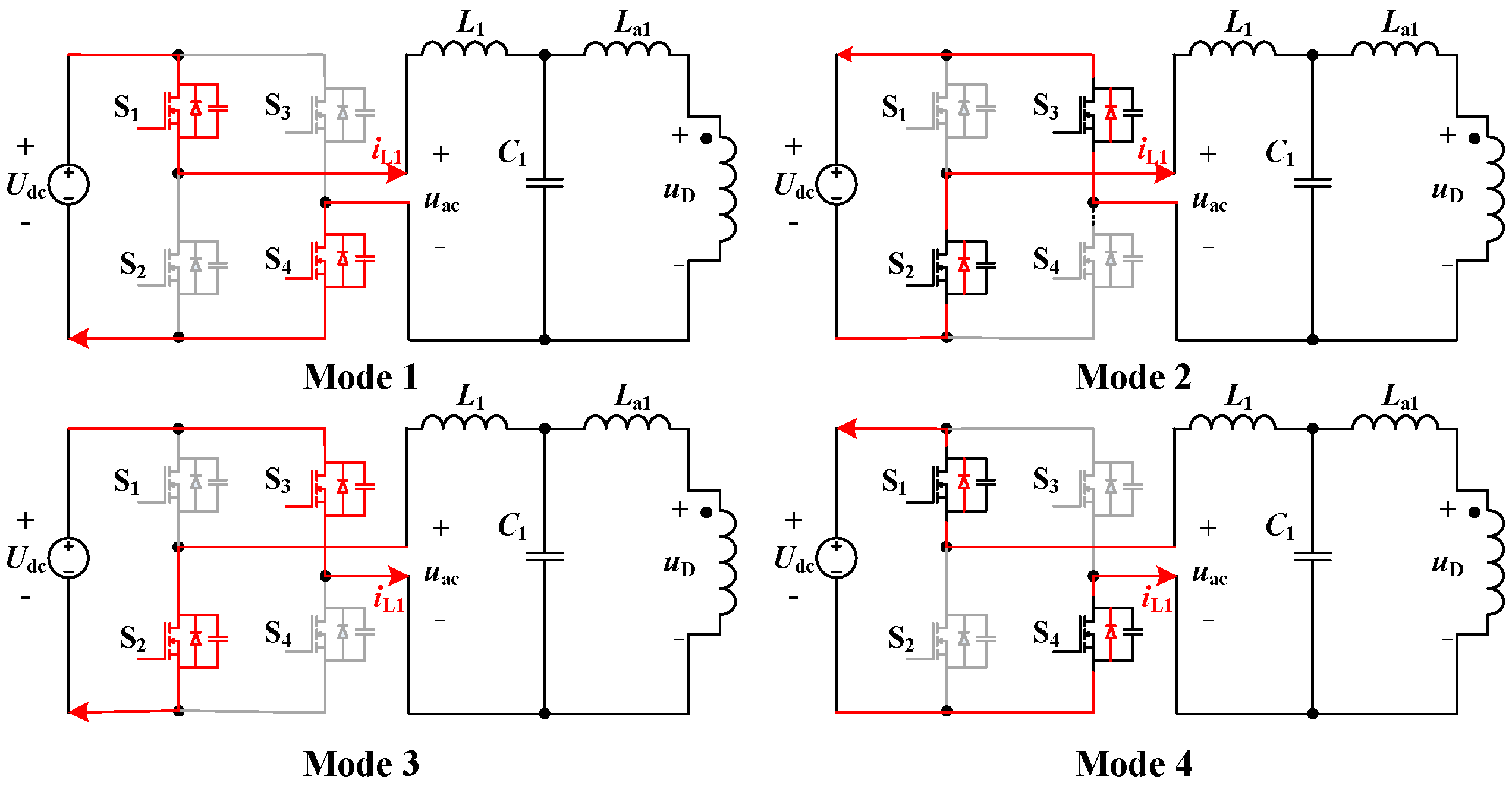
As illustrated in
Figure 3, the converter operates in four primary modes within a single switching period, with the current paths highlighted in red and with inactive switching devices marked in gray. By employing phase-shift control, the full-bridge inverter converts the input DC voltage,
Udc, into a high-frequency square-wave voltage,
uac.
The operational modes are analyzed as follows:
In Mode 1, switches S1 and S4 are in the ON state. The DC power source forms a loop through S1, the LCL-T resonant network, and S4, transferring energy to the network.
In Mode 2, all the switches are turned OFF. The energy stored in the resonant inductor is released through the freewheeling diodes of S2 and S3, allowing the current to continue circulating.
In Mode 3, switches S2 and S3 are in the ON state. A reverse DC voltage is now applied to the input of the resonant network, and current flows through S3, the resonant network, and S2.
In Mode 4, S2 and S3 are turned OFF, and all the switches are once again in the OFF state. The energy in the resonant inductor is released through the freewheeling diodes of S1 and S4. This completes one full operational cycle.
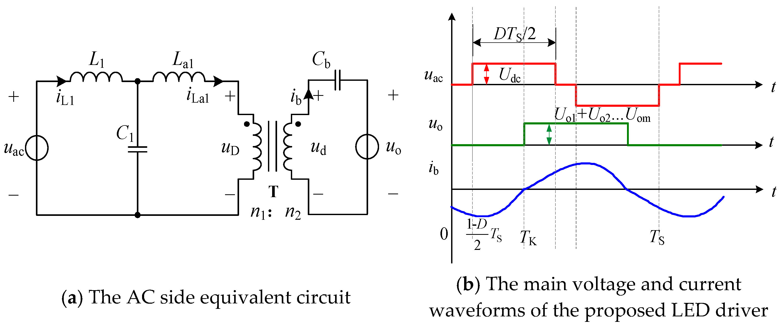
Figure 4a displays the analogous circuit for the AC side. Phase-shifting full-bridge PWM control is applied to switches S
1–S
4. S
1 and S
2, and S
3 and S
4 are turned ON and OFF complementarily, respectively. S
1 and S
3 have the same duty cycle, and their phase difference is 180°. Thus, as seen in
Figure 4b, the full-bridge DC/AC inverter’s output voltage is a high-frequency AC square voltage,
uac. The square voltage,
uo, serves as the diode rectifier’s input voltage. The amplitude of
uo is equal to the sum of the LED load voltages when the current,
ib, is larger than 0. The amplitude of
uo equals 0 when the current,
ib, is smaller than 0.
As described in
Figure 4b, the LCL resonant network,
uac, input voltage can be written as:
where
D is the switching device’s conduction duty cycle, and
TS is its switching period.
According to the above analysis of the square voltage,
uo, it can be expressed as follows in the first switching cycle.
where
Uo =
Uo1 +
Uo2 +... +
Uom,
m is the number of output channels, and
TK is the starting delay time of the output voltage,
uo, square wave.
Both
uac and
uo are AC square voltages, so their Fourier series expansion can be easily obtained as:
where
And the voltage,
uo, can be expressed as
where
DC-blocking capacitor
Cb filters out the DC component of the high-frequency square voltage,
uo, which is
Uo/2. Therefore, the LCL resonant network output voltage,
uD, may be written as
where
Additionally, N is the transformer T’s turns ratio, which is equivalent to n1/n2.
The output currents of each LED string are identical since they are linked in series via the diode rectifier, which means
Figure 2 shows that the precise output current,
Io1-act, is equivalent to half of the average value of the current,
ib, during the positive half-switching phase. So, if the currents
ib or
iLa1 can be obtained quantitatively, the exact solution of the output current
Io1-exa can be obtained, which is derived as
Next, the characteristics of the output current are analyzed considering the fundamental and higher harmonics, respectively.
2.1. Only Considering the Fundamental Harmonic
The ratio of inductors
L1 and
La1, the resonant angular frequency, ω
o, and its normalized angular frequency, ω
n, are defined as
where
fS is the switching frequency, and ω
S represents its angular frequency.
The LCL-T rectifier functions as an ideal current source if the resonant angular frequency is equivalent to the switching frequency, or ω
n = 1, and only takes into account the fundamental harmonic in voltage
uac and
uD [
21]. Accordingly, as examined in [
21], the output current,
Io1, is independent of the output voltage, and it can be expressed as
The LCL-T resonant network parameters may be found using Equations (7) and (8). If Uac1m, N, and Io1 are known, the inductor, L1, can be calculated from (8), and the capacitor C1 can be deduced from (7).
The determination of the inductor,
La1, is as follows. When
γ is equal to 1, the fundamental component of the resonant network input current,
iL1, is in phase with the fundamental component of the voltage,
uac, as concluded in [
21]. The resonant network should be slightly inductive to achieve the zero-voltage switching conditions for switches, so
γ needs to be greater than 1. As
γ is taken as 2 here, it is also verified that it is a reasonable value in
Section 3. Next,
La1 can be calculated from (8) once
L1 and
γ are determined.
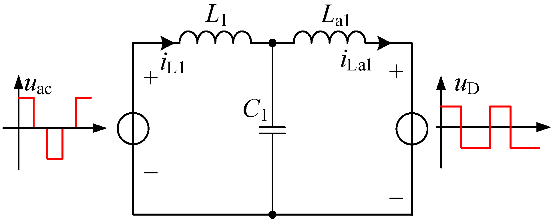
2.2. Considering Higher Harmonics
Figure 5 below represents the analogous circuit of the LCL-T resonant network seen in
Figure 4a. There are many higher harmonics in the current
iLa1 because the voltages,
uac and
uD, of the LCL-T network correspond to the AC square voltages from (3) and (5), and these include considerably higher harmonics. It is crucial to carefully examine how higher harmonics affect the precision of the output currents, since (7) will have an impact on the accuracy of the precise output current,
Io1-exa.
In
Figure 5,
iLa1 can be solved when the voltage sources,
uac and
uD, work separately. Then, the final current,
iLa1, can be obtained according to the superposition theorem. The expressions of
uac and
uD are shown in (3) and (5), and the phase of the AC voltage,
uD, is determined by
TK, which is solved as follows.
The AC voltage,
uD, crosses zero when
t =
TK, and the inductor current,
iLa1, also crosses zero at this time, that is,
iLa1(
TK) = 0. In order to determine the connections between
TK,
Udc,
N, and
Uo using the frequency domain analysis approach, Equation (10) is obtained from [
21]. The output current,
Io1-exa, can thus be precisely solved as (11). Finding the precise current solution and examining the parameters needed to satisfy the output current’s accuracy criteria are the primary uses of Equation (11).
After determining
Udc,
N,
D, and
Uo,
TK may be solved using mathematical programs like MATLABR2024a, as stated in [
21]. Then, the precise solution of the output current,
Io1-exa, is obtained as follows:
As indicated by (10) and (11), Io1-exa is a function of Udc, Uo, N, D, and L1. Therefore, the subsequent step is to determine the parameters, N and L1. The architecture of the LCL-T passive resonant rectifier provides the conditions necessary to achieve zero-voltage switching (ZVS), the realization of which is ensured by the proper selection of the parameter γ.
To validate the preceding theoretical analysis, a corresponding simulation model was constructed. As depicted in
Figure 6, the simulation results clearly demonstrate that the input voltage,
uac, (red trace) is a square wave with an amplitude of ±400 V, while the output voltage,
uD, (blue trace) is also a square wave that lags
uac. This outcome is in good agreement with the theoretical analysis for the equivalent voltage at the output of the LCL-T resonant network, thus verifying the correctness of the theory presented in this section.
The primary function of the LCL-T resonant network is to perform waveform shaping. Through the analysis and calculation of inductor L1 and capacitor C1, its resonant frequency is set to the switching frequency. The network exhibits low impedance to the fundamental component of the square-wave voltage, uac, while presenting high impedance to higher-order harmonics. Furthermore, the presence of the inductor, La1, effectively attenuates high-order harmonics. The DC-blocking capacitor, Cb, connected in series with the transformer secondary, serves to filter out any DC bias resulting from various factors, thereby ensuring the stable operation of the entire resonant network. In summary, owing to the filtering effect of the LCL-T network and the DC-blocking protection afforded by Cb, the system successfully converts the square-wave voltage into a smooth, high-quality AC.
3. Parameter Design
The stable state model of the whole system, taking into account only the fundamental harmonic, may be obtained using Equations (3) and (9):
By linearizing (12) around the steady-state operating point (
D,
Io), the influence of a duty cycle perturbation on the output current can be obtained. This is defined as the system’s DC gain,
Kdc:
Through the output filtering stage, the system’s low-frequency dynamic properties are established. The output filter for this topology may be roughly represented via the first-order RC low-pass filter, and the transfer function,
H(
s), is as follows:
where
Co is the output filter capacitance, and
RLED is the equivalent resistance of the LED load.
By combining the DC gain and low-frequency dynamic characteristics obtained from the above analysis, the small-signal transfer function,
G(
s), can be obtained as follows:
Equation (15) was derived using the fundamental harmonic approximation (FHA) method, which represents the open-loop small-signal transfer function of the entire system. This model abstracts the controlled object as a first-order system with variable gain Kdc, primarily used to analyze the low-frequency dynamic characteristics of the system and lay the groundwork for subsequent feedback controllers.
To verify the correctness and accuracy of this theoretical model, a simulation model of the proposed LED driver was constructed in MATLAB/Simulink.
Since the simulation’s circuit parameters act as a direct reference for the practical prototype, they are extremely important. The simulation was configured with a DC input voltage, Udc, of 400 V and a switching frequency, fs, of 100 kHz. To reduce the physical volume of the resonant network, the transformer turns ratio, N, was set to 2 after detailed analysis. For a target constant output current, Io, of 0.7 A, with the normalized angular frequency, ωn, set to 1 and the inductor ratio, γ, preset to 2, Equations (8) and (9) were used to compute the LCL-T resonance network’s constants. This yielded the following values: L1 = 364.5 μH, La1 = 182.25 μH, and C1 = 6.96 nF.
To validate the accuracy of the theoretical model, the transfer function,
G(
s), derived from the theoretical analysis, is compared against
Gf(
s) obtained from the simulation model.
Figure 7 presents a comparison of the theoretical and simulated Bode plots. As illustrated in the figure, the Bode plot derived from the theoretical calculation is in good agreement with the frequency-sweep simulation results, thereby validating the correctness of the established mathematical model in the low-frequency domain.
Following the simulation verification, the subsequent step involves preparing for the experimental implementation. To design a closed-loop controller capable of fast and precise output current regulation, a thorough understanding of the system’s model characteristics is essential. The small-signal function of transfer
G(
s) from the obligation cycle,
d(
s), to the output current,
io(
s), demonstrates the traits of a conventional first-order low-pass filter, as per Equation (15):
where the pole ω
p = 1/(
RLED ·
Co).
By substituting the relevant circuit parameters, it can be calculated that the system pole, fp, is 19.5 Hz. The system’s dynamic reaction time is quite sluggish because of the pole’s relatively low frequency, which prevents it from meeting the necessary requirements for quick adjustment and quick startup.
Additionally, the duty cycle,
D, change affects the DC gain,
Kdc. When duty cycle
D is zero, the worst-case situation arises, and
Kdc achieves its maximum value, represented by
Kdc_max:
Following the above theoretical analysis, the designed PI controller needs to meet four requirements. To enhance the system’s dynamic reaction speed, the bandwidth must first be increased (fc = 10 kHz). Secondly, it is also necessary to ensure that the system has a sufficient stability margin to resist parameter changes and external disturbances. Thirdly, the compensated system must eliminate the steady-state error, which is the basic requirement for maintaining a constant output current. Fourth, the system also needs to reduce overshoot to protect the LED components and extend their service life.
After analysis, by appropriately adjusting the PI parameters, the proportional–integral controller can meet the above four requirements.
In this section, three distinct PI controller design methods are compared, all based on the worst-case gain scenario. These methods are the zero-pole cancellation method, the phase margin tuning method, and the pole placement method. A comparative analysis of various performance metrics will be conducted to determine the most suitable design approach for the experiment.
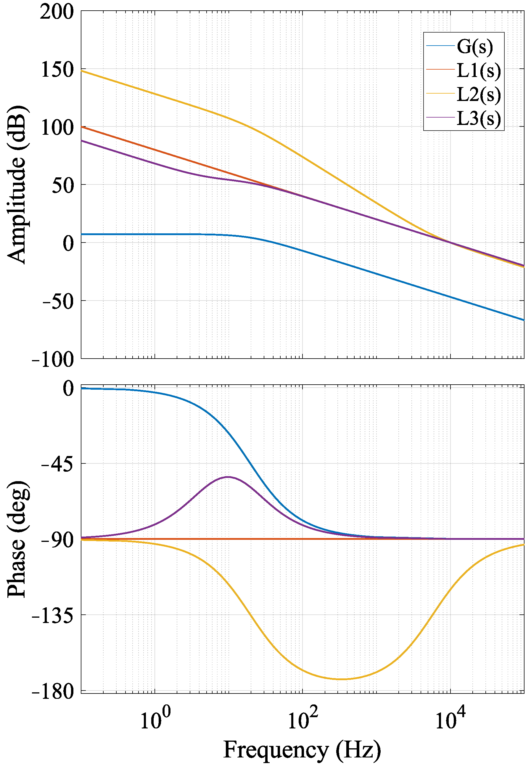
To provide a clear visual comparison, the open-loop transfer functions resulting from each of the three methods are plotted using MATLABR2024a, as shown in
Figure 8. In the figure, the uncompensated system is represented by the curve,
G(
s), while the systems compensated using methods one, two, and three are represented by
L1(
s),
L2(
s), and
L3(
s), respectively. Meanwhile, after calculation, various data of the open-loop curves in the figure are supplemented in
Table 1 for convenient comparison and analysis.
The plant model, based on the system parameters, is:
The resulting open-loop transfer functions corresponding to the curves L1(s), L2(s), and L3(s) are as follows:
For
L1(
s): The controller
Gc1(
s) precisely sets its zero point at the pole of the controlled object, thereby achieving zero-pole cancellation and simplifying the system to a pure integrator form.
For
L2(
s): By reasonably designing the parameters of controller
Gc2(
s), the system can achieve the specified phase margin. The complete open-loop transfer function is:
For
L3(
s): The controller,
Gc3(
s), uses the pole placement method for its zero location. The complete open-loop transfer function is:
The transfer functions of L1(s), L2(s), and L3(s) are obtained through the above theoretical calculations. Based on their transfer functions, the corresponding Bode plots can be drawn.
By analyzing the performance metrics of each curve in
Table 1 and the frequency response characteristics shown in
Figure 8, the zero-pole cancellation method (Method 1) is the most suitable compensation strategy for this application. Its principle lies in aligning the controller’s zero with the main pole of the controlled object, achieving precise cancellation functionally, thereby transforming the open-loop transfer function into an approximate ideal integrator. This method exhibits excellent robustness, characterized by a 90-degree phase margin and zero overshoot characteristics, which protect the LED load from overcurrent hazards. Given the significant advantages of the zero-pole cancellation method, this method is also adopted in the subsequent experimental verification to design the PI controller.
4. Experimental Verification and Analysis
The preceding sections explain the operating principle of the converter, analyze and derive the mathematical model and small-signal model of the system, and design the most suitable PI controller for this paper based on theoretical analysis.
Based on the above system analysis and controller design, this section constructs a complete closed-loop control system, as shown in
Figure 9. In order to verify the validity of the aforementioned analysis and parameter design, a five-channel experimental prototype with a rated power of 200 W was constructed, and its detailed specifications are the same as those listed in
Table 2. The corresponding circuit components are also listed in the same table. The control strategy comprises the following: firstly, the current of a single output channel is sampled; secondly, this is compared with a preset reference signal to generate an error signal; thirdly, the error signal is processed by a PI compensator to output a modulating signal; and finally, the modulating signal is compared with a triangular carrier to generate PWM signals to drive the four power switches. The series connection of the output channels via rectifier circuits enables the system to achieve effective closed-loop control of all output currents. As illustrated in
Figure 9, the block diagram depicts the closed-loop control system, with its core control unit implemented using a TMS320F28335 digital signal processor.
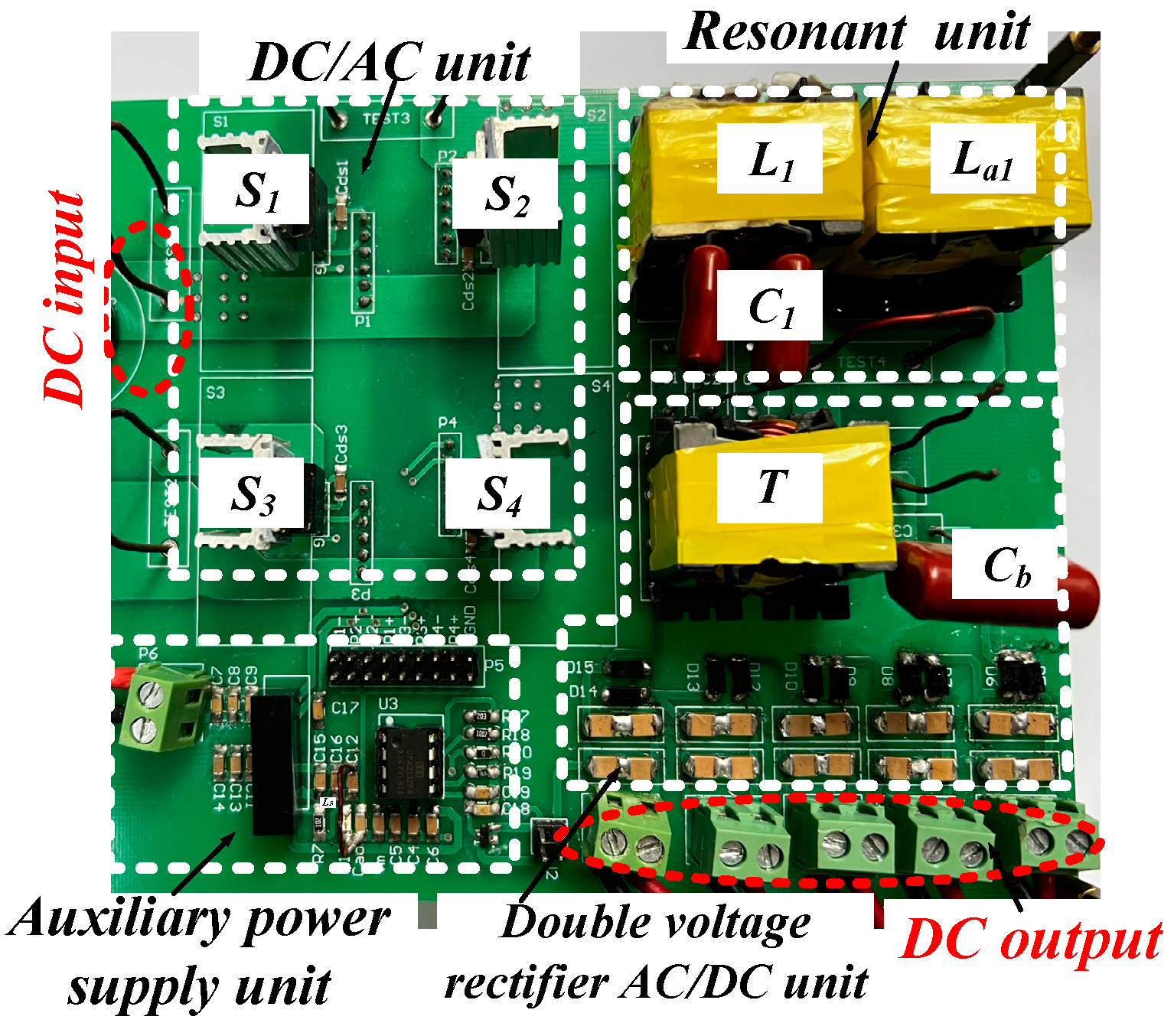
Figure 10 is a photograph of the experimental prototype.
In the control circuitry of the experimental prototype, the isolated gate driver is a critical component. The isolated driver circuit employed in this study is depicted in
Figure 11, wherein pwm3 is the PWM input signal. The gate driver IC, IC1 (NSi6602B-DSWR), converts the logic-level pulse (PWM3) from the controller into a high-frequency square-wave drive signal. This conversion is achieved by its internal push–pull output stage, which alternately applies high and low levels across the PWMC and GNDC output terminals, connected respectively to the gate and source of the power MOSFET. The switching frequency of the MOSFET is set to 100 kHz.
4.1. Experimental Waveform Analysis
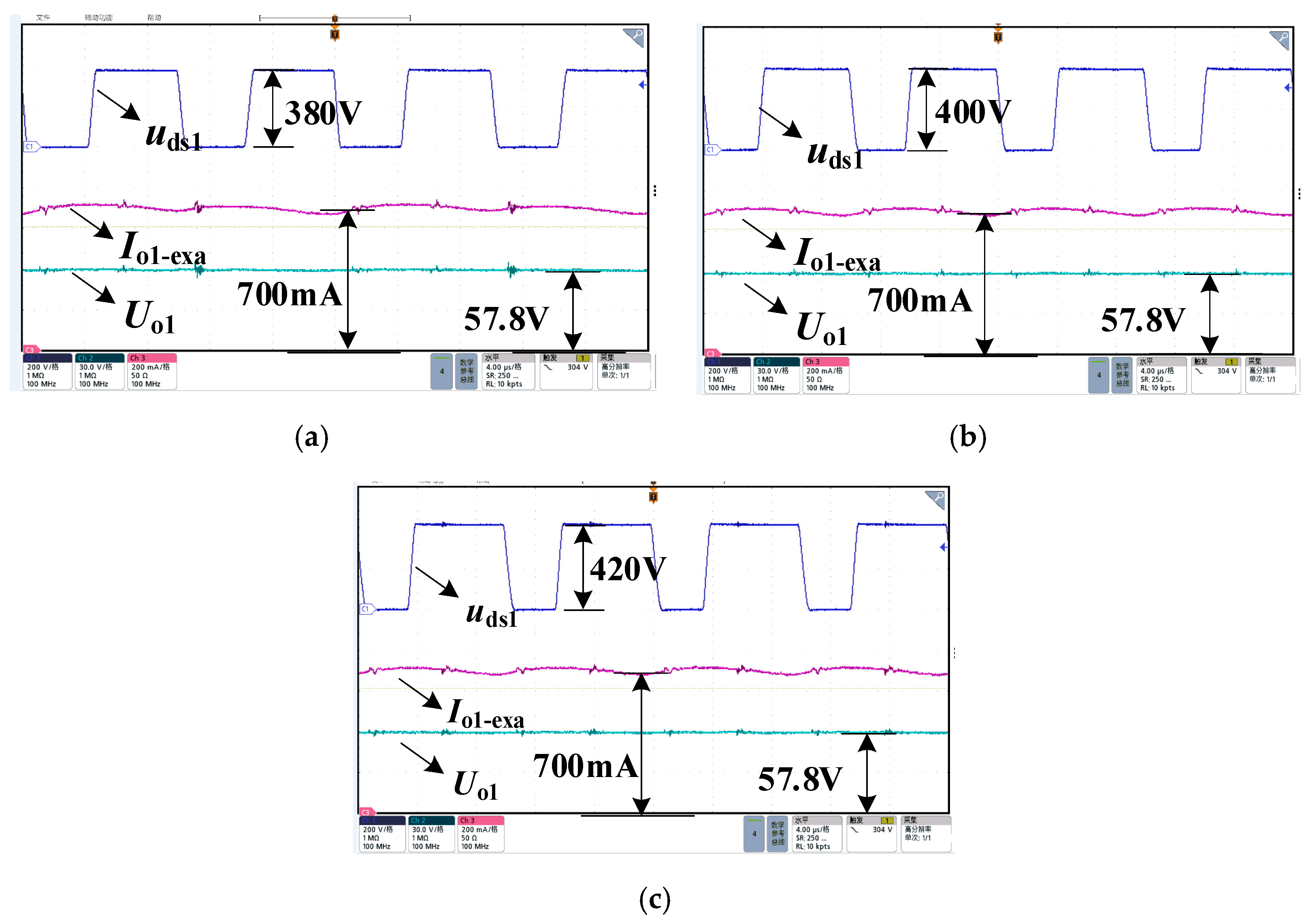
This section presents the performance verification results of the experimental prototype. As shown in
Figure 12a–c, the waveform diagrams illustrate the steady-state output waveforms under rated power and different input voltage conditions. The figure shows the experimental waveforms under operating conditions with input voltages,
Udc, of 380 V, 400 V, and 420 V. In each subfigure, the waveforms from top to bottom are the drain–source voltage of switch S
1 (
uds1), the channel output current (
Io1-exa), and the final output voltage (
Uo1). The experimental data indicate that the output current, Io1-exa, remains at a constant level of 700 mA within the input voltage range of 380 V to 420 V. This experimental result validates the effectiveness of the closed-loop control strategy and meets the system design specifications for high-precision output current requirements.
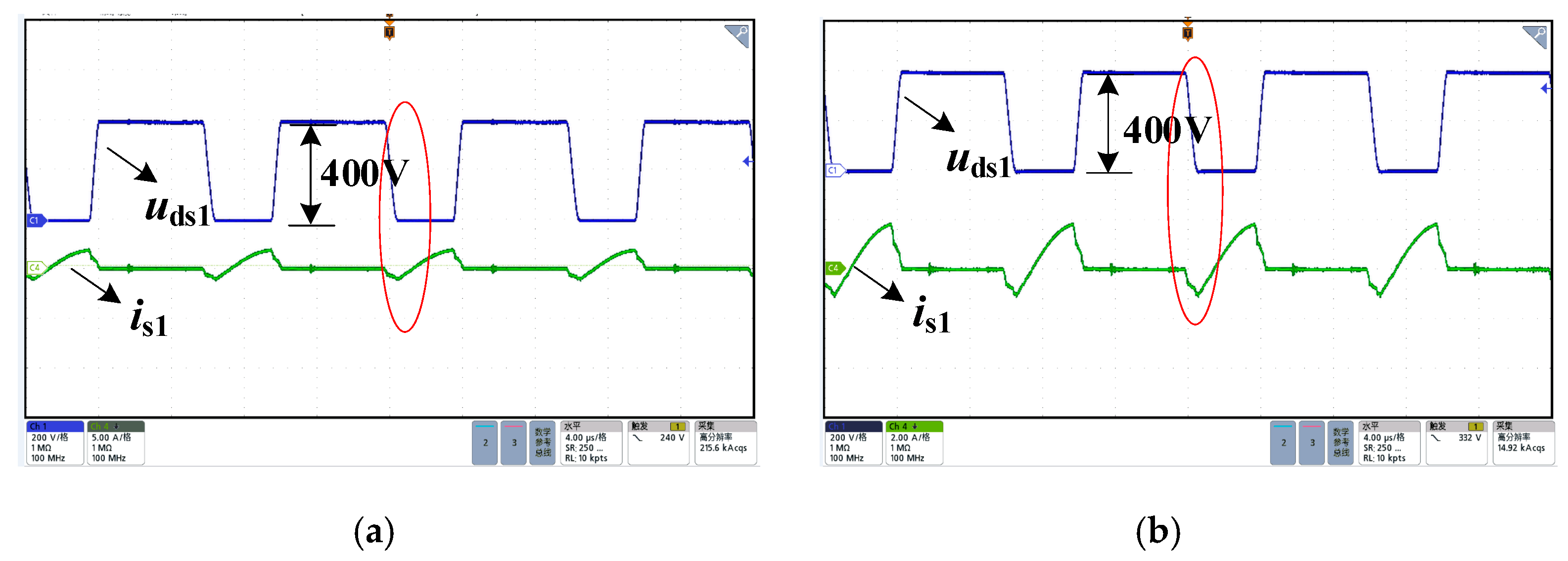
The objective of this study is to verify the zero-voltage switching (ZVS) conditions described in the theoretical analysis of the first part by employing switch transistors S
1 and S
3 as research objects and utilizing experimental characteristic analysis methods. As demonstrated in
Figure 13a, under operating conditions of input voltage
Udc = 400 V and output power
P = 200 W, the drain–source voltage (
uds1) and channel current (
is1) waveforms of switch transistor S
1 were measured. As illustrated in
Figure 13b, the measured values correspond to the drain–source voltage (
uds3) and channel current (
is3) of switch transistor S
3. The experimental data suggest that the currents,
is1 and
is3, are both negative prior to each transistor switching operation. This negative state has been proven to cause the anti-parallel diodes to enter a forced conduction state. This finding confirms that the switching transistors, S
1 and S
3, have successfully achieved zero-voltage switching (ZVS) operation.
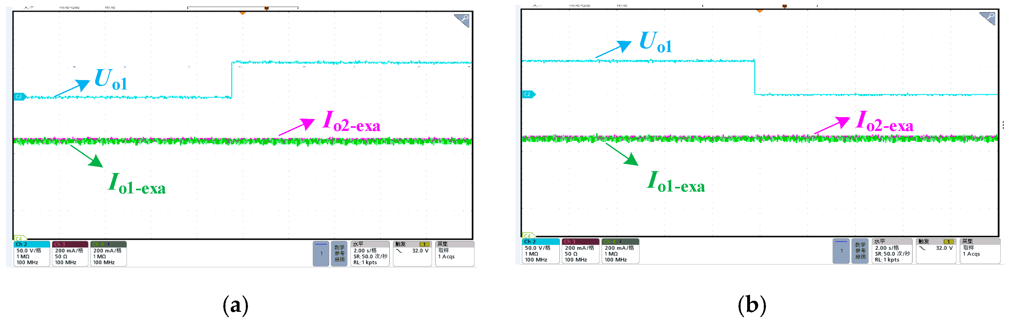
Figure 14 shows transient waveforms when the input voltage,
Udc, changes at rated power 200 W.
Figure 15 shows transient waveforms when the output voltage,
Uo1, changes. Taking the first and second output channels as an example, the waveforms in
Figure 14 are the input voltage,
Udc, and the output currents,
Io1-exa and
Io2-exa. As illustrated in
Figure 15, the dynamic waveforms of the output voltage,
Uo1, and the output currents,
Io1-exa and
Io2-exa, are also shown. The experiment demonstrates that, in conditions of load disturbance, the output current can rapidly revert to the set value within a brief timeframe. This outcome validates the efficacy of closed-loop control for all output channels and substantiates the accuracy of the output current, which aligns with the design specifications across the entire operational range.
4.2. Loss Analysis and Theoretical Efficiency Estimation
By thoroughly analyzing the wear and tear on each component, we have provided a theoretical basis for proving the high efficiency of the system.
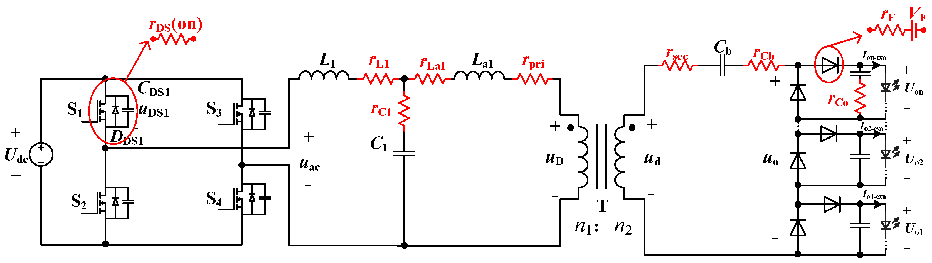
Figure 16 illustrates the loss model of the converter, which incorporates the primary parasitic components inherent in the circuit elements. These components include the on-resistance (
rDS(on)) of the MOSFET, the forward voltage drop (
VF) and on-resistance (
rF) of the diode, the parasitic resistance (
rL1 and
rLa1) of inductors
L1 and
La1, the parasitic resistance of capacitors
C1 and
Cb (
rC1 and
rCb), and the primary and secondary winding resistances of the transformer (
rpri and
rsec), which are the fundamental sources of power loss. Based on this model, the power loss calculations for each component are as follows.
The total conduction loss of the four switches can be calculated based on the effective value,
IL1,rms, of the current,
iL1, flowing through the AC side of the inverter:
This topology achieves zero-voltage switching (ZVS) through phase shift control, so switching losses can be ignored. Losses mainly originate from the switching process, and the switching loss of a single switch can be expressed as:
where
fS is the switching frequency, and
CDS1 is the output capacitance of the MOSFET.
Therefore, the total MOSFET loss is:
Diode conduction losses are caused by both the forward voltage drop,
VF, and the equivalent dynamic resistance,
rF. The diode loss for a single channel is:
where
Idiode,rms is the effective value of the current flowing through a single rectifier diode.
The loss of inductance is mainly caused by copper loss generated by parasitic resistance,
rL. For inductances
L1 and
La1 in this circuit, the total loss is:
where
IL1,rms and
ILa1,rms are the effective values of the alternating current flowing through the corresponding inductors.
Capacitor loss is caused by its parasitic resistance,
rC. The total capacitor loss is:
where
IC1,rms,
ICb,rms, and
ICo,n,rms are the effective values of the alternating current flowing through the corresponding capacitors.
Transformer losses include copper losses and iron losses:
where
Ipri,rms and
Isec,rms are the effective values of the primary and secondary currents, respectively, and
Pcore,T is the magnetic loss.
Adding up all of the above loss components to obtain the total theoretical loss of the converter results in:
To theoretically assess the efficiency of the proposed converter, the theoretical efficiency of the system can be estimated by the following equation:
This section provides a quantitative analysis of the primary power loss sources in the system, based on device datasheets, circuit simulations, and standard engineering estimation methods. Under rated operating conditions, the calculated theoretical total loss is approximately 9.45 W, corresponding to an efficiency of 95.5%. Among these losses, the rectifier diodes account for the largest portion, exceeding 58%, followed by the core loss of the magnetic components (approx. 21%) and the conduction loss of the MOSFETs (approx. 10%).
4.3. Experimental Efficiency Analysis
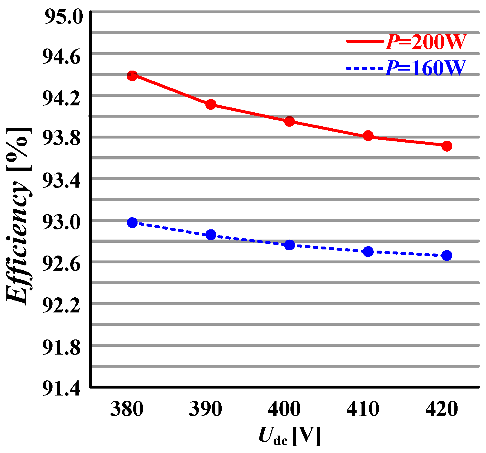
To validate the accuracy of the theoretical analysis, efficiency tests were conducted on the prototype.
Figure 17 presents the measured efficiency curves under various input/output conditions. The experimental results indicate that the efficiency of the topology improves significantly as the output load increases, with a measured peak efficiency of 94.4% being achieved under rated operating conditions.
In summary, the experimental tests confirm the precise control capability of the apparatus over the output voltage and current. This measured value is in close agreement with the theoretical peak efficiency of 95.5%, with the minor discrepancy being primarily attributed to unmodeled parasitic parameters and measurement errors. This result further validates the correctness of the design methodology and its practical engineering value.


