1. Introduction
The LLC resonant converter has gained widespread adoption as one of the most prevalent isolated DC-DC converter topologies, owing to its high efficiency, high power density, and excellent soft-switching characteristics [
1,
2,
3,
4]. This topology finds extensive applications in critical domains, including on-board battery chargers (OBCs), server and telecommunication power supplies, industrial automation equipment, medical power supplies, LED lighting drivers, and renewable energy systems [
5,
6,
7].
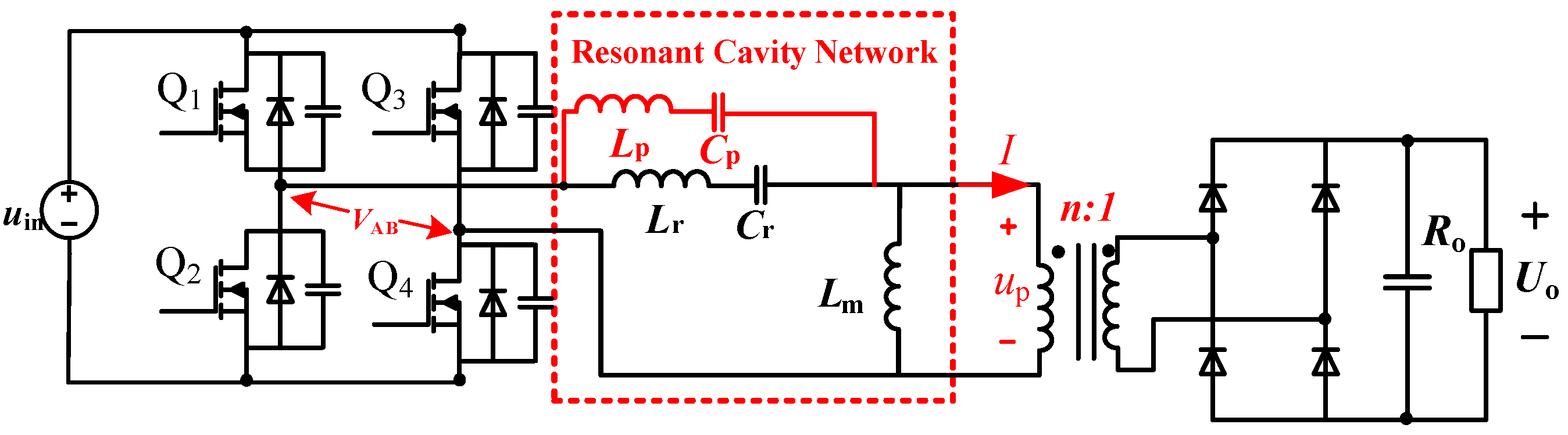
Figure 1 illustrates the circuit configuration of a conventional full-bridge LLC resonant converter incorporating a full-bridge rectifier stage. In LLC resonant converters, the power transfer mechanism is inherently facilitated through the resonant circuit (comprising inductor
Lr and capacitor
Cr) and the isolation transformer. As schematically depicted in
Figure 1, the application of a square-wave voltage waveform at the
VAB node establishes a sinusoidal current profile within the resonant
Lr–
Cr network. This alternating current is subsequently propagated to the secondary side through magnetic coupling in the transformer, enabling energy delivery to the load [
8,
9,
10]. The voltage regulation mechanism in an LLC resonant converter is realized by modulating the switching frequency of switches
Q1–
Q4. This modulation dynamically alters the impedance division ratio within the resonant tank, thereby controlling the output voltage [
11]. This operational principle enables precise control of the voltage conversion gain, thereby maintaining a stabilized output voltage
Uo under varying load conditions.
Pulse frequency modulation (PFM) is widely used in LLC resonant converters, adjusting the switching frequency to modulate resonant tank impedance [
12]. However, above resonance, PFM-controlled LLC converters exhibit reduced voltage gain sensitivity at higher frequencies, complicating wide voltage-range applications (e.g., on-board chargers and solar systems) [
13,
14]. These scenarios require excessively broad frequency ranges to meet strict gain specifications, increasing magnetics complexity, compromising zero-voltage switching, and degrading EMI performance [
15,
16,
17,
18]. To address these limitations while achieving extended voltage gain within narrow frequency bands, numerous research approaches have been proposed from different technical perspectives.
Based on the modification locations, LLC resonant converters can be categorized into three distinct subcategories: primary-side inverters, resonant tanks, and secondary-side rectifiers. In [
19], a novel topology was introduced featuring an additional switch integrated into the primary full-bridge inverter, dual independent resonant tanks (
Lr/
Cr), transformers, and full-wave rectifiers. This configuration enables multi-mode operation through primary switch state regulation, significantly expanding the achievable voltage gain range. However, the incorporation of redundant components, particularly magnetic elements, substantially increases circuit complexity and manufacturing costs while compromising power density. In [
20,
21], different basic topologies, such as Buck–Boost and Buck, are cascaded with an LLC resonant converter to achieve extremely high voltage conversion ratios. However, this approach suffers from significant drawbacks, including highly complex system control and potentially slow dynamic response.
A fractional magnetizing inductance with a parallel-connected auxiliary switch was presented in [
22]. By actuating the auxiliary switch, the resonant tank configuration can be dynamically reconfigured to operate in different states. Various secondary-side rectification schemes have been proposed in [
23,
24,
25,
26,
27]. Notably, ref. [
27] replaced the conventional full-wave rectifier with a reconfigurable voltage-doubler rectifier capable of operating in Type-4, Type-5, and Type-6 configurations. Nevertheless, the achievable gain ranges of existing rectification topologies remain constrained, which inevitably expands the required frequency variation range and consequently limits potential application scenarios.
To enable the proposed converter to achieve a wide voltage gain range within a narrow frequency band, this paper introduces a multi-element resonant converter methodology by incorporating one or two additional inductors/capacitors into the conventional LLC resonant tank structure. This approach generates multiple resonant frequencies in the system transfer function, thereby enhancing the gain characteristics. Through comparative analysis of the gain profiles across these derived LLC resonant converter topologies, the configuration with optimal gain performance is selected for detailed investigation. The resonant tank configurations of the proposed LLC-derived topologies are illustrated in
Figure 2.
Through systematic modeling and parametric analysis of the voltage gain characteristics for LLC derivative topologies 1 through 9, the gain expression for each topology is established based on the Fundamental Harmonic Approximation (FHA) method. Subsequently, their dynamic voltage gain curves as a function of normalized frequency are plotted using a consistent set of parameters. Building upon this, a comparative analysis is conducted by plotting the gain curves of the derivative topologies alongside those of the conventional LLC resonant converter on the same set of axes. The results are illustrated in
Figure 3, where the red curves represent the gain of the derivative topologies and the blue curve corresponds to that of the conventional LLC converter.
Image analysis reveals that Topology 4 demonstrates significantly superior gain range compared to other configurations. This ultra-steep gain characteristic enables stable high-frequency output under wide input voltage scenarios while allowing substantial voltage regulation through minimal frequency adjustments. Such performance effectively reduces switching device stress, making it particularly suitable for high-dynamic applications. Consequently, Topology 4 is selected as the primary research subject and designated as the L-LCLC resonant converter in this study.
By controlling the connection/disconnection of additional inductors and capacitors through switching devices, the L-LCLC resonant converter achieves structural reconfiguration to enhance the voltage gain range. Compared to the LLC topology, the L-LCLC configuration requires additional reactive components but achieves superior gain characteristics. To optimize overall system efficiency, a hybrid control strategy is implemented: the converter operates in L-LCLC mode when the switching frequency exceeds the resonant frequency, and transitions to LLC mode under sub-resonant conditions. The mode transition occurs precisely at unity voltage gain, where both topologies share identical operating frequencies and gain values. This design methodology effectively minimizes voltage/current stress during mode transitions while maintaining high efficiency across the entire operational range.
The contributions of this study are summarized as follows: (1) This paper presents a detailed analysis of the voltage gain characteristics for the L-LCLC resonant converter, accompanied by a complete derivation of the governing mathematical equations. Furthermore, the soft-switching operational regions of the converter are systematically delineated through a thorough steady-state analysis. Based on these findings, a systematic parameter design methodology is also proposed. (2) A hybrid mode transition strategy is implemented to improve overall system efficiency. The converter seamlessly switches between LLC and L-LCLC modes at the unity gain point, where both topologies share identical operating frequencies and gain characteristics. This design effectively mitigates transient voltage and current surges during mode transitions while maintaining high efficiency across the entire operational range.
The organization of this paper is structured as follows:
Section 1 reviews key challenges in LLC resonant converters and explains the motivation for the L-LCLC topology.
Section 2 provides a detailed analysis of the L-LCLC converter’s operational principles, covering gain characteristics, soft-switching properties, and hybrid mode transitions.
Section 3 proposes a design methodology for critical components, highlighting optimization of the parallel inductor
Lp and capacitor
Cp.
Section 4 validates theoretical analysis via simulations, while
Section 5 confirms performance through experimental testing on a 100 W prototype.
Section 6 summarizes contributions and practical implications.
2. Principal Analysis of Converter
2.1. The Equivalent Model of the Circuit and the Gain
Figure 4 illustrates the circuit configuration of the L-LCLC resonant converter. Compared to the conventional LLC topology, this configuration incorporates an additional inductor
Lp and capacitor
Cp within the resonant cavity network.
The L-LCLC resonant converter is modeled using the fundamental harmonic approximation method. By linearizing the operational characteristics of the high-frequency transformer and composite resonant tank network at the fundamental frequency, an AC equivalent circuit model incorporating core resonant components is established. The simplified equivalent circuit diagram of the L-LCLC resonant converter is illustrated in
Figure 5. In
Figure 5,
Ei represents the input voltage to the resonant tank, while
Ip,
Ir, and
Im are the currents flowing through capacitor
Cp, capacitor
Cr, and inductor
Lm, respectively.
Eo denotes the overall output voltage of the resonant converter.
Based on the fundamental harmonic analysis method, the secondary-side equivalent resistance
Req of the transformer can be derived as
By formulating the KVL/KCL, the system characteristics can be derived as
By solving the aforementioned system of equations, the following expressions can be derived as
The reciprocal of the L-LCLC resonant converter’s voltage gain in the frequency domain can be formulated as
The L-LCLC resonant converter exhibits three distinct resonant frequencies f1 = 1/2π, f2 = 1/2π, f3 = /2π. The converter’s gain profile is defined by three critical resonant frequencies. At switching frequencies f1 and f2, the converter achieves a unity voltage gain. This occurs because series resonance—between Lr and Cr at f1, and between Lp and Cp at f2—causes the equivalent impedance of the resonant branch to approach zero, allowing the output voltage to approximate the input voltage. When operating at f3, the entire Lr-Cr-Lp-Cp network transitions into parallel resonance, creating an infinite equivalent impedance across the resonant branch. This state effectively blocks energy transfer to the output, and the converter gain is approximately zero.
2.2. Soft-Switching Characteristics Analysis
As derived from
Figure 5, the input impedance
Zin of the L-LCLC resonant network can be expressed as
The normalized frequencies are defined as
fn1,
fn2, and
fn3, where
Rac =
Reqn2,
fn1 =
fs/
f1,
fn2 =
fs/
f2,
fn3 =
fs/
f3, and where
fs denotes the switching frequency. The structural voltage gain G can be expressed as
where T =
/
Rac,
P1 = (
λ1λ3 +
λ1λ3)/(
λ2 +
λ2λ3)
fn12 − 1,
P2 = 1 −
λ1λ3fn12/
λ2,
P3 = (1 −
fn12)/
fn1(1 +
λ3),
λ1 =
Lm/
Lr,
λ2 =
Lm/
Lp,
λ3 =
Cp/
Cr.
When the input impedance
Zin exhibits purely resistive characteristics, the voltage gain becomes inherently resistive and can be derived as
Based on Equations (6) and (7), the inherently resistive voltage gain curves and parametric gain curves for varying
T values can be plotted, as illustrated in
Figure 6. In the
Figure 6, the number 1 represents the blue area, number 2 represents the yellow area, and number 3 represents the pink area.
The operational zones of the L-LCLC resonant converter are categorized into three distinct regions, defined by the purely resistive characteristic curve and the boundary line fn1 = 1:
Region 1: Located to the left of both the boundary line fn1 = 1 and the purely resistive characteristic curve, the converter exhibits capacitive behavior and operates in the ZCS mode.
Region 2: Positioned to the left of the boundary line fn1 = 1 and to the right of the purely resistive characteristic curve, the converter exhibits inductive behavior. Here, the voltage gain G > 1, indicating a step-up operation mode, with the system functioning in the ZVS regime.
Region 3: Positioned to the right of the boundary line fn1 = 1 and to the left of the purely resistive characteristic curve, where the voltage gain G < 1 indicates a step-down operation mode, with the system operating in the ZVS regime.
The operational analysis of the L-LCLC resonant converter focuses on switching frequencies below f3, as frequencies exceeding f3 are excluded from practical design considerations. To prioritize ZVS operation, the converter should be designed to operate in Region 3, as established in the preceding analysis.
2.3. Mode Transition Strategy
As illustrated in
Figure 7, the voltage gain curves of the two resonant converters reveal distinct operational characteristics. Under the LLC frequency-modulation (FM) mode, the converter operates in a step-up configuration, whereas the L-LCLC structure-variable frequency modulation mode enables step-down operation. Since a mode switch is required, we should select an appropriate switching point.
Two conventional methods exist for determining mode transition points. The first is based on equal efficiency between operational modes, requiring loss calculations (conduction/switching) in both modes, but faces computational complexity and numerical instability. The second prioritizes resonant frequency proximity, balancing voltage gain stability and efficiency sensitivity to frequency deviations. In this study, both converter modes operate under frequency modulation control and share a common resonant frequency point. At this specific switching frequency, both modes achieve unity voltage gain with zero frequency deviation, significantly mitigating voltage/current stress during mode transitions. Therefore, this resonant frequency point is selected as the optimal mode transition point.
3. Parameter Design
Extensive research has been conducted by scholars on the circuit parameter design of LLC resonant converters [
28,
29,
30,
31,
32]. Building upon these foundations, this paper presents a systematic parameter design methodology for the additional parallel-connected inductor and capacitor introduced in the L-LCLC resonant converter topology.
Based on the hybrid control strategy definition, the LLC FM mode operates under minimum input voltage conditions, achieving the maximum voltage gain
Gmax. Conversely, the L-LCLC FM mode functions at maximum input voltage, yielding the minimum voltage gain
Gmin. With constant output voltage maintained, the following relationships hold:
As established in the operational characteristics, the LLC frequency modulation mode operates in the step-up region (
G > 1), whereas the L-LCLC structure-variable FM mode functions in the step-down region (
G < 1). Under these conditions, the voltage gain relationship can be derived as
The peak gain, denoted as
Gpeak, is fully utilized by setting
Gpeak0 =
Gmax. To ensure design robustness, a 20% safety margin is incorporated. The available peak gain
Gpeak0 can thus be calculated as
To ensure the converter operates in the LLC FM mode when the switching frequency is below
fn1, and achieves steeper voltage gain curves beyond the mode transition point compared to the LLC FM mode, the composite parallel resonant frequency of the
Lr-
Cr-
Lp-
Cp network must exceed the series resonant frequency of the
Lr-
Cr branch. This condition guarantees optimal performance across both operational modes.
To prevent the voltage gain from collapsing to zero, the composite parallel resonant frequency of the
Lr-
Cr-
Lp-
Cp network should be designed to exceed the converter’s maximum switching frequency
fsmax. This condition ensures operational stability across the entire frequency modulation range while maintaining inherent voltage regulation capability.
The parametric design methodology initiates with selecting an appropriate
λ3 value within the typical operational range of 0.1–0.5 for the L-LCLC resonant converter operating in regulated output mode. Based on Equation (6), different
λ2 values are sequentially evaluated to satisfy the predefined gain constraints, thereby establishing the feasible
λ2 range. Within this range, the optimal
λ2 parameter is determined according to specific gain sensitivity requirements. Following
λ2 selection, an inverse iterative process is implemented: maintaining the chosen
λ2 while re-evaluating
λ3 variations under identical gain constraints to determine its optimized range. The final
λ2/λ3 parameters are then consolidated through this bidirectional optimization process. Substituting these optimized values into Equations (14) and (15) subsequently yields the concrete specifications for
Lₚ and
Cₚ components. The systematic parameter selection flowchart is illustrated in
Figure 8.
Taking the design process presented in this paper as an example, the design procedure is initiated by setting
λ3 = 0.2, followed by evaluating multiple
λ2 values to generate the gain profiles illustrated in
Figure 9a. The optimal
λ2 value of 2.6 is determined based on the specified gain sensitivity requirements. Subsequently, an iterative refinement process adjusts
λ3 variations while maintaining the selected
λ2, producing the gain characteristics shown in
Figure 9b. Through comparative analysis of these gain profiles,
λ3 is finalized at 0.25, considering both sensitivity optimization and operational margin. The inductance
Lₚ and capacitance
Cₚ parameters are then calculated by substituting the optimized
λ2/
λ3 set into Equations (14) and (15). The final design parameters of the converter, including the optimized
Lₚ and
Cₚ values, are systematically summarized in
Table 1.
4. Simulation Study
To validate the feasibility of the proposed methodology, a Simulink (MATLAB R2024a version)-based simulation study is first conducted. The simulation was performed using a discrete solver with a sample time of 5 ns. The parasitic capacitance of each primary-side switching device was set to 1.5 nF. The switching frequency is regulated by a Proportional–Integral (PI) controller to maintain a stable output voltage. Furthermore, the engagement of the
Lp and
Cp branches is dynamically controlled. This is achieved by continuously sampling the input and output voltages to calculate the real-time converter gain. Based on this gain, the branch is disconnected from the circuit when the gain is greater than one and reconnected when the gain is less than one. The key parameters of the converter, including component values and operational specifications, are presented in
Table 1.
Figure 10a,b present the simulated waveforms of the capacitor
Cr current
Icr and output voltage illustrating two operational scenarios:
Figure 10a input voltage
Uin = 160 ± 20 V with regulated output voltage
Uo = 200 V. From top to bottom, the waveforms represent input voltage, output voltage, and capacitor current. As shown in
Figure 10b, when
Uin decreases from 180 V to 140 V, the output voltage maintains stable regulation around 100 V. Similarly, when
Uin increases from 210 V to 250 V, the output voltage remains tightly regulated at 100 V. This demonstrates excellent voltage regulation stability across wide input voltage variations, enabling the converter to adapt to applications requiring different voltage levels.
Figure 11a,b present the voltage, current, and power waveforms of primary-side switching devices, along with gate trigger voltage signals, at switching frequencies of 150 kHz and 220 kHz, respectively. As observed in both subfigures, during switch turn-on transitions, no overlap occurs between voltage and current waveforms, resulting in zero turn-on loss. This confirms the successful realization of ZVS, which aligns precisely with theoretical predictions.
5. Experimental Result
A 100 W experimental prototype is established to verify parameter design. The specifications of the experimental prototype are consistent with
Table 1.
Figure 12 shows the photograph of the experimental prototype.
Figure 13 presents a comparative analysis of voltage gain characteristics between the LLC and L-LCLC resonant converter modes under a 200 V input voltage.
Figure 13a,b illustrate the experimental waveforms of square-wave input voltage
VAB and output voltage at a switching frequency of 160 kHz for LLC and L-LCLC modes, respectively.
Figure 13c,d display corresponding results at 228 kHz. At 160 kHz, both modes exhibit output voltage fluctuations around 200 V. However, when operating at 228 kHz, the LLC mode produces an output voltage of approximately 130 V, while the L-LCLC mode achieves a significantly lower output voltage of 40 V. This demonstrates the L-LCLC configuration’s ability to extend the voltage gain range by over 300% compared to the conventional LLC topology, validating its superior performance in wide-gain applications.
Figure 14a,b illustrate the experimental waveforms of the current
I and output voltage under an input voltage of 200 V and switching frequency of 160 kHz, corresponding to output powers of 100 W and 75 W, respectively. From top to bottom, the waveforms represent output voltage, current
I, square-wave input voltage
VAB, and gate-source voltage of the switches. As shown in the left figure, at full load (100 W), the output voltage remains stably regulated around 200 V. Similarly, the right figure demonstrates that even at reduced load (75 W), the output voltage maintains tight regulation at approximately 200 V. This confirms the converter’s robust voltage regulation capability across varying load conditions, enabling its application in scenarios with diverse power requirements.
As shown in
Figure 15, during the transition from LLC to L-LCLC mode, the output voltage remains stably regulated around 200 V, demonstrating excellent transient stability. This confirms the effectiveness of the hybrid control strategy in maintaining output regulation during structural reconfiguration.


