Article

Active-Clamp Dual-Transformer ZVS Flyback Converter

1
Department of Electrical Engineering, National Taipei University of Technology, No. 1, Sec. 3, Zhongxiao E. Rd., Taipei 10608, Taiwan
2
Department of Electrical Engineering, Feng Chia University, No. 100, Wenhwa Road, Seatwen, Taichung 40724, Taiwan
*
Author to whom correspondence should be addressed.
Energies 2025, 18(13), 3331; https://doi.org/10.3390/en18133331
Submission received: 9 June 2025 / Revised: 23 June 2025 / Accepted: 23 June 2025 / Published: 25 June 2025

Abstract

In order to upgrade the ability of the traditional flyback converter to transfer energy to the load, a dual-flyback converter with two active clamping circuits is added, using the same clamping capacitor to recover the leakage inductance energy. Furthermore, no additional resonant inductor is needed, and both the switches have zero voltage switching (ZVS) to reduce the switching loss. In addition, full-wave rectification is used on the secondary side to decrease the output voltage ripple frequency, which makes it easy to design the output filter.

1. Introduction

Power supply can be classified into two types: switching and linear. The former has the advantages of higher power density and higher efficiency. In recent years, switching power supplies have moved towards increasing the switching frequency to reduce the overall circuit size, thereby achieving high power density [1,2]. Switching methods can be classified into hard switching and soft switching. However, the former will experience switching loss. Consequently, in order to reduce the loss caused by the switching of switches, the soft switching method has been introduced There are four common technologies used for this, as described below.
(1)
Resonant Converter [3]
In order to solve the problem of low hard-switching efficiency, since the early 1980s, the literature [1] has described resonant converters with the capacitor connected in parallel with the switch or the inductor connected in series with the switch to form the LC resonant circuit. This is the first paper to address the concept of soft switching. When the voltage on the switch resonates to zero, the power switch is turned on to achieve zero voltage switching (ZVS); when the current in the switch resonates to zero, the switch is turned off to achieve zero current switching (ZCS). Although these techniques can improve the overall efficiency of the converter, the corresponding disadvantage is that the resonance generates a relatively large voltage and current. This not only adds extra voltage stress or current stress to the components, but also creates relatively serious conduction losses.
(2)
Quasi-resonant Converter (QRC) [4]
The quasi-resonant converter is designed to minimize switching losses by adding a winding and a sensor to detect the valley voltage on the switch. However, the quasi-resonant switching technique is not completely ZVS, and this structure requires variable-frequency control and operation in the discontinuous conduction mode (DCM). In addition, in order to improve the efficiency, the secondary side mostly adopts synchronous rectification (SR), but due to the unpredictability of the turn-on time, it is usually necessary to use an external SR chip to detect the current at zero point for switching to reduce the loss.
(3)
Zero Voltage/Zero Current Transition (ZV/ZCT) [5,6,7,8,9,10,11,12]
ZV/ZCT is a technique in which an auxiliary switch is transiently resonated before the main power switch is energized by means of an external circuit to reduce the stress on the switch, and at the same time to achieve ZV/ZCS of the switch.
However, when ZV/ZCT converters [5,6,7,8] were first developed, the converter was able to achieve ZV/ZCS of the main switch by means of an auxiliary circuit, but it was not possible to achieve ZV/ZCS of the auxiliary switch, since the auxiliary switch transfers the energy from the main power switch to the auxiliary switch, thereby resulting in heat buildup on the auxiliary switch. Accordingly, the literature [9] proposes adding ZV/ZCS to the auxiliary switch to reduce the switching loss. According to the literature [10,11,12], the auxiliary switch is turned on before the switch is turned on and off, so that the switch has ZVT and ZCT.
(4)
Active Clamp Converter [13,14,15,16,17,18,19,20]
Active clamp technology improves the efficiency of the converter by making the voltage on the switch as close to zero voltage as possible when the switch is turned on. The principle of this technology is to connect a clamping capacitor in series with an auxiliary switch, which can be used for energy storage and energy recycling functions when the main switch is turned on and off, respectively. In other words, before the main switch is turned on, the energy stored in the output parasitic capacitor of the switch is released to the clamping capacitor to realize ZVS; when the main switch is turned off, the auxiliary switch releases the energy stored in the clamping capacitor.
The literature [13] proposes a primary-side regulation (PSR) method to analyze and derive the equations, and then the results are used to compensate the secondary losses to improve the accuracy of the output voltage regulation. The literature [14] proposes an active-clamped flyback converter and an automatic adjustment of the length of the blanking time in each state to achieve ZVS under various operating conditions.
In recent years, an active clamping circuit has been applied to boost converters in [15,16,17,18,19], and both the main switch and the auxiliary switch are able to achieve ZVS.
On the other hand, most of the low and medium power DC/DC converters on the market use a flyback converter. Since the flyback converter is directly connected to the transformer, the leakage inductance energy of the transformer will cause the switch to be subjected to high-frequency spike and ringing voltages during the cutoff period. Traditionally, in order to solve this problem, a snubber is added to the primary side of the transformer [20]. This snubber circuit generally consists of capacitors, resistors, and diodes, which can effectively absorb the energy generated by voltage surge into the capacitor during the switch cutoff moment, and then transfer this energy to the resistor to be consumed when the switch is turned on. However, although this method can effectively reduce high-frequency spike and ringing voltages, the efficiency is quite low. Consequently, active-clamped ZVS flyback converters [13,14,15] have been proposed, not only to recycle leakage inductance energy but also to achieve ZVS turn-on of the main switch.
In this paper, an active-clamped dual-transformer ZVS flyback converter is presented to increase the ability of the traditional flyback converter to transfer energy to the load. To achieve ZVS, no additional magnetic components are required in the resonant tank.

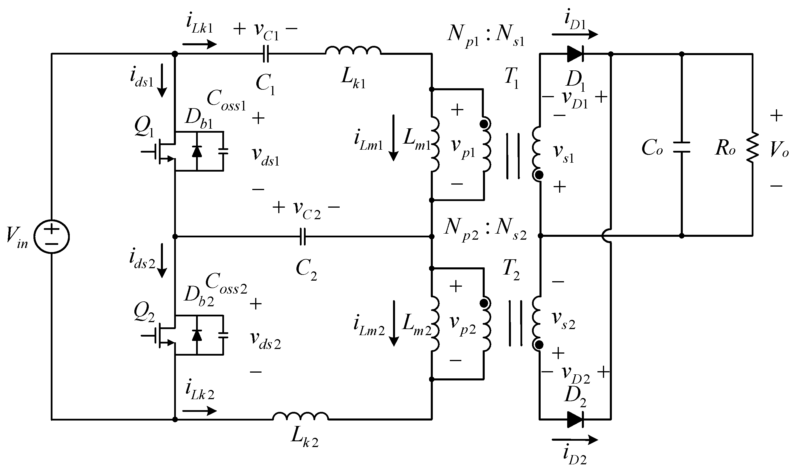
2. Proposed Active-Clamp Dual-Transformer ZVS Flyback Converter

Figure 1 shows the active-clamp flyback converter with two transformers. This circuit consists of an auxiliary switch Q1, a main power switch Q2, a clamping capacitor C1, an energy-transferring capacitor C2, an output capacitor Co, two output rectifier diodes D1 and D2, two transformers T1 and T2. In addition, the load side is represented by an output resistor Ro.

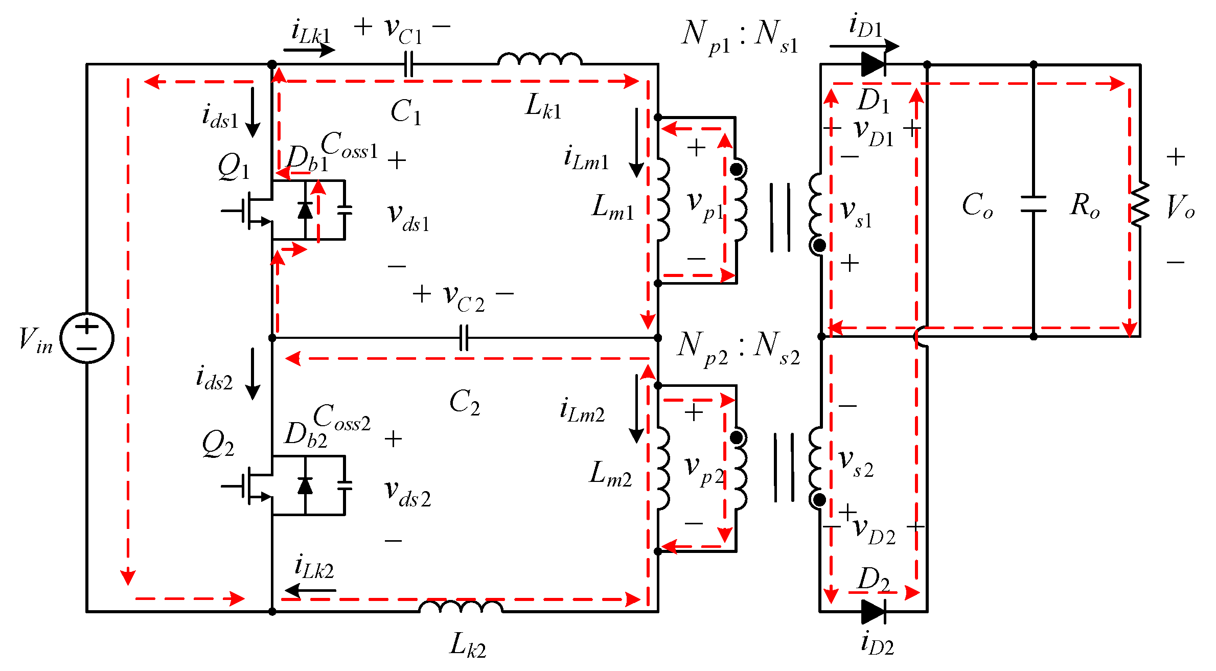
2.1. Symbol Definitions and Assumptions

Prior to describing the operating principle of this circuit, the relevant variables in Figure 1 are defined as follows:
(1)
Vin is the input DC voltage, the output capacitance Co is large enough, and the output voltage is denoted as Vo.
(2)
Db1 and Db2 are the body diodes of the auxiliary switch Q1 and the main switch Q2, respectively; Coss1 and Coss2 are the output capacitors of the auxiliary switch Q1 and the main switch Q2, respectively.
(3)
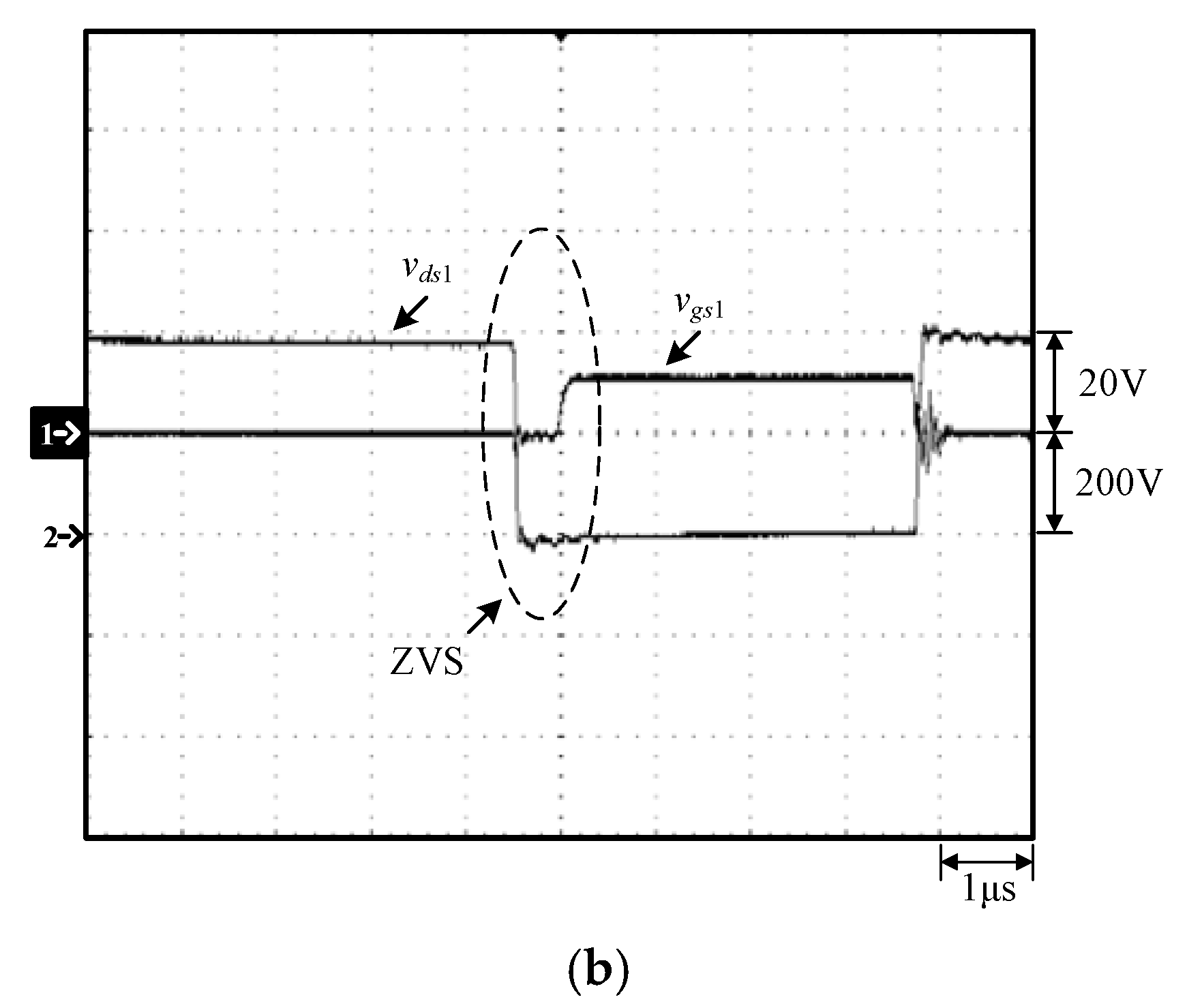
ids1 and ids2 are the currents in the auxiliary switch Q1 and the main switch Q2, respectively; vds1 and vds2 are the voltages on the auxiliary switch Q1 and the main switch Q2, respectively; vgs1 is the gate driving signal for the auxiliary switch Q1, vgs2 is the gate driving signal for the main switch Q2, and these two signals are complementary signals, namely, 1 − D and D for Q1 and Q2, respectively.
(4)
Lk1 and Lk2 are the leakage inductances of the first transformer and the second transformer, respectively, and are also the resonant inductances; Lm1 and Lm2 are the magnetizing inductances of the first transformer and the second transformer, respectively.
(5)
iLk1 and iLk2 are the leakage inductance currents of the first transformer and the second transformer, respectively, and are also the resonant inductor currents; iLm1 and iLm2 are the magnetizing inductance currents of the first transformer and the second transformer, respectively.
(6)
Np1 and Ns1 are the turns of the primary and secondary sides of the first transformer, and their turns ratio is n 1 = N p 1 N s 1 ; Np2 and Ns2 are the turns of the primary and secondary sides of the second transformer, and their ratio is n 2 = N p 2 N s 2 ; let n 1 = n 2 = n .
(7)
vp1 and vp2 are the primary-side voltages of the first transformer and the second transformer, respectively; vs1 and vs2 are the secondary-side voltages of the first transformer and the second transformer, respectively.
(8)
vC1 and vC2 are the voltages on the clamping capacitor C1 and the energy-capacitor C2, respectively.
(9)
vD1 and vD2 are the voltages on two output rectifier diodes D1 and D2, respectively; iD1 and iD2 are the currents in two output rectifier diodes D1 and D2, respectively.
(10)
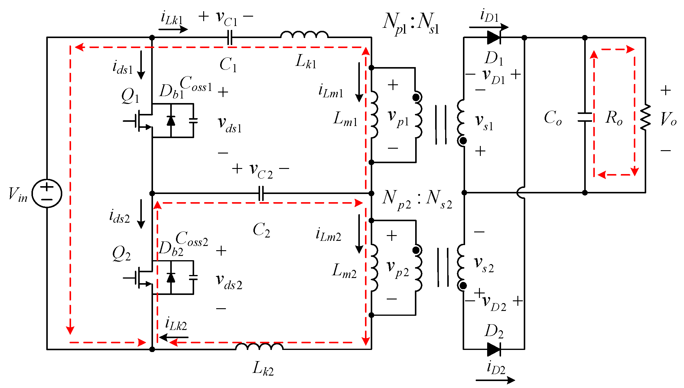
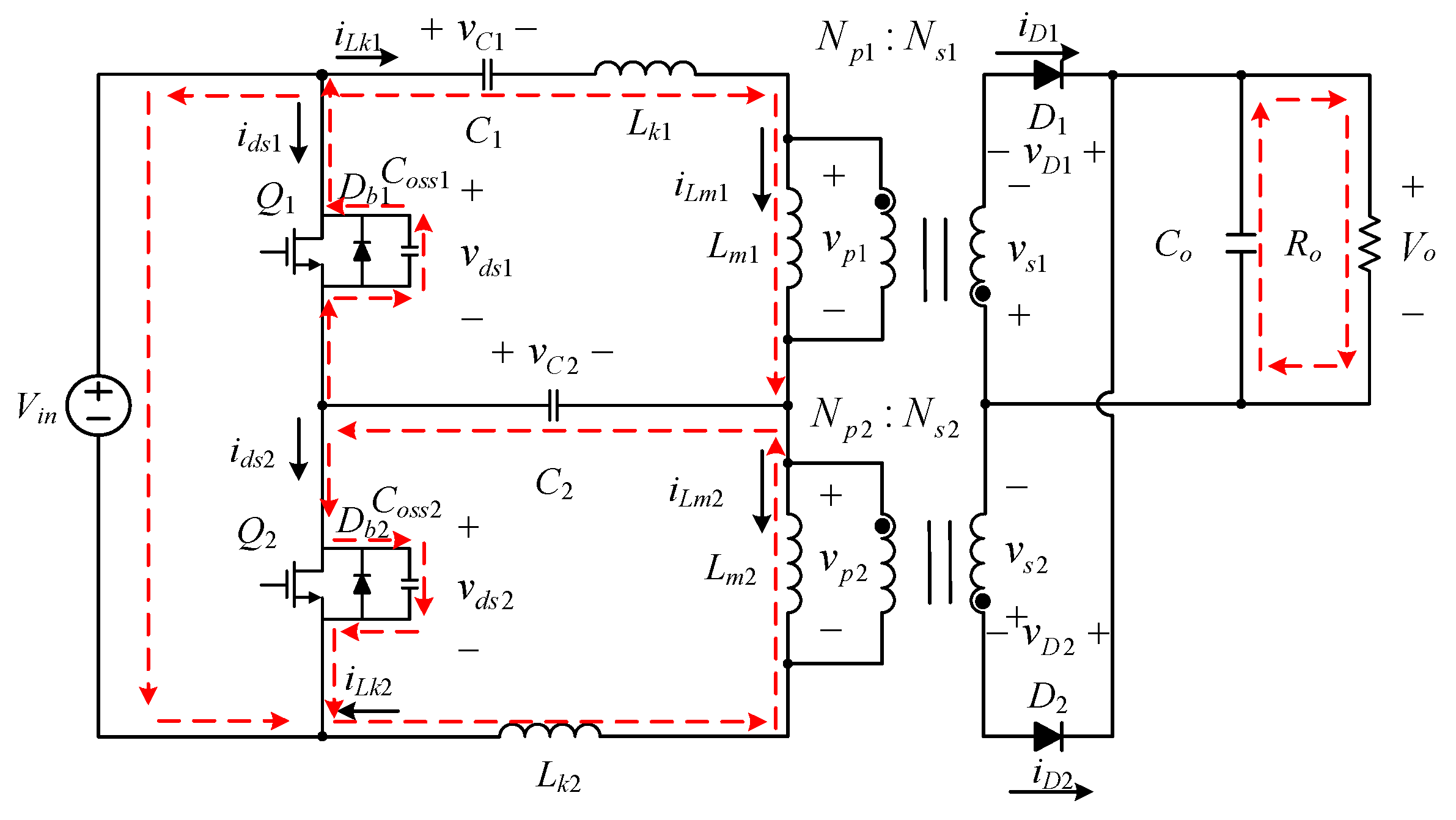
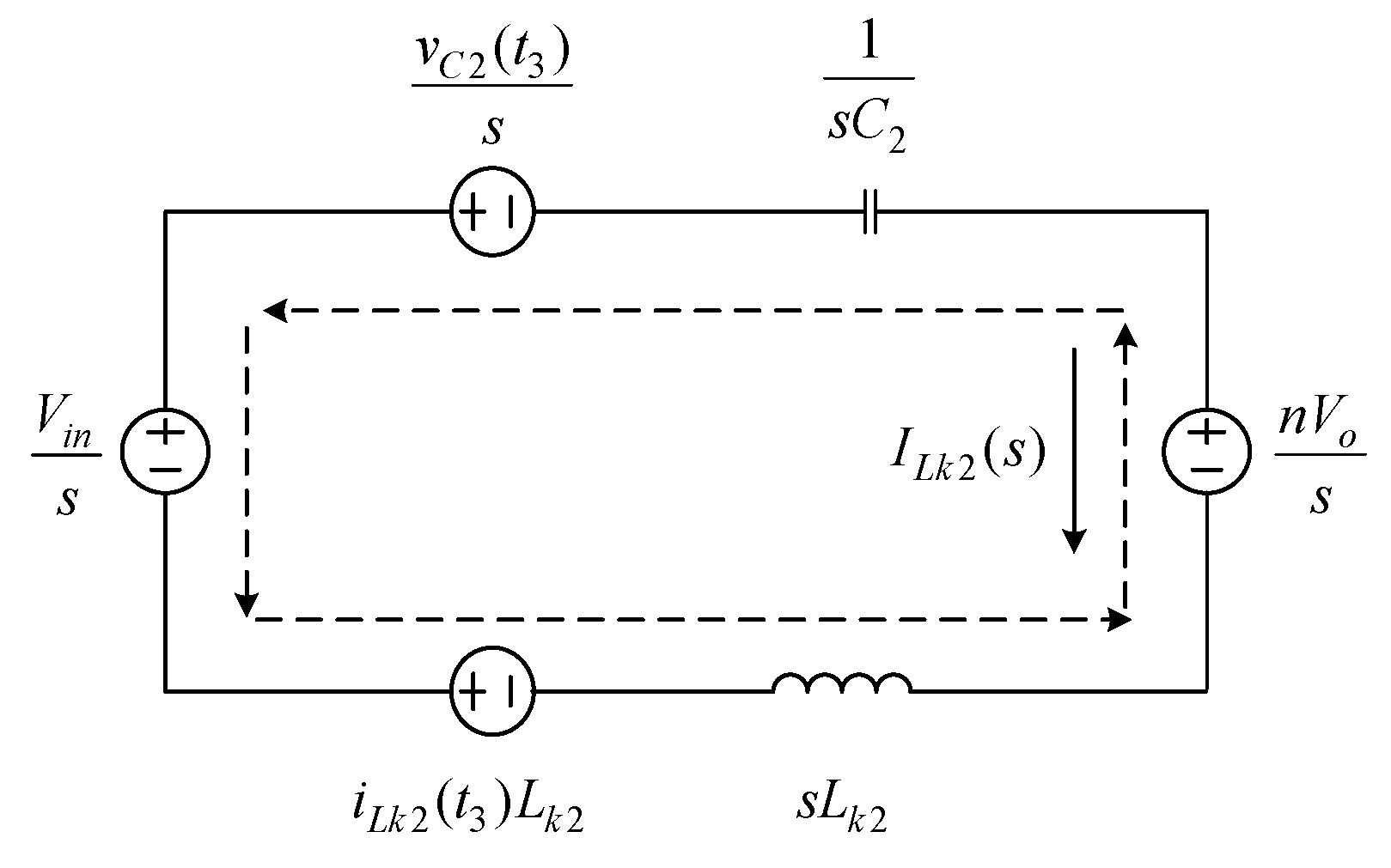
For brief analysis convenience, the circuit is operated under positive and negative currents, and Figure 2 shows the behavior of the circuit in one cycle. For brief analysis convenience, only the time interval between t0 and t6 will be taken into account; that is, the positive magnetizing current of T1 and the negative magnetizing current of T2 both occurring at the same time will be discussed.

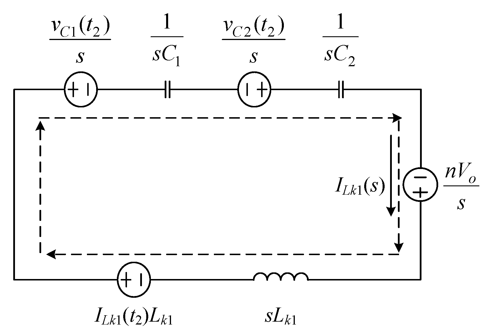
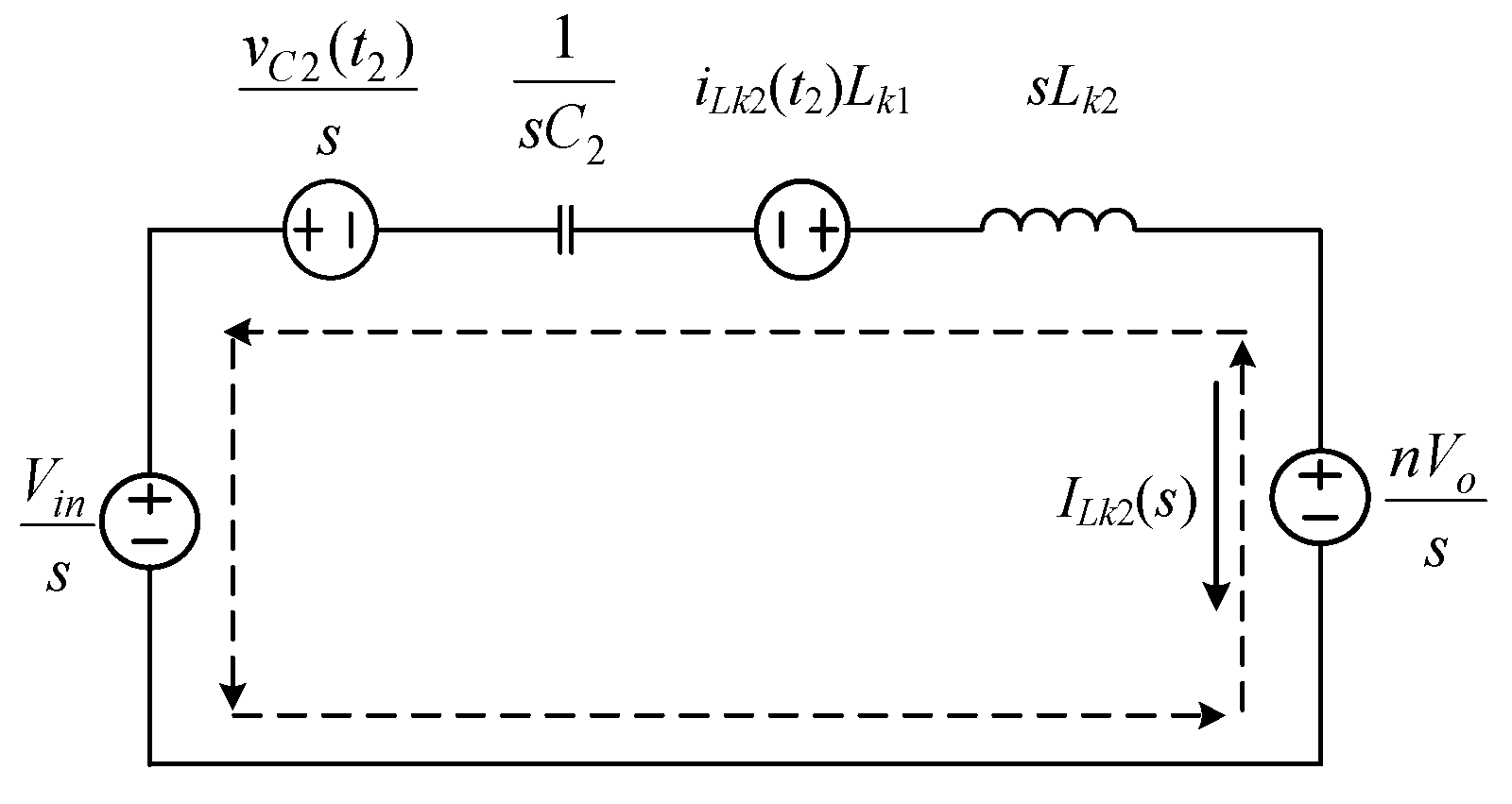
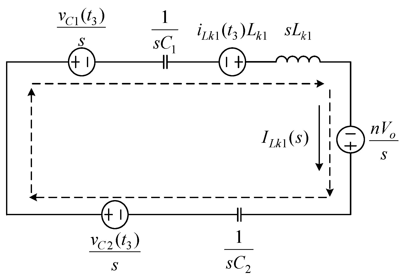
2.2. Operating Principle
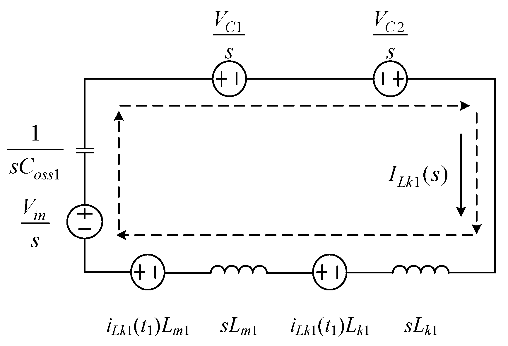
State 1 [t0tt1]: As shown in Figure 3, the auxiliary switch Q1 is off and the main switch Q2 is on. Assume vC1(t0) and vC2(t0) are constant. During this state, the voltage across the magnetizing inductance Lm1 of the first transformer is VinvC1(t0) + vC2(t0) (ignoring the voltage on Lk1), so the magnetizing inductance Lm1 is energized, whereas the voltage across the second inductance Lm2 of the second transformer is −vC2(t0) (ignoring the voltage on Lk2), so the magnetizing inductor Lm2 is de-energized. In addition, the energy required at the load side is supplied by the output capacitor Co. As t = t1, the main power switch Q2 is turned off, and this state ends. The corresponding equations are as follows:
i L k 1 ( t ) = i L k 1 ( t 0 ) + V i n v C 1 ( t 0 ) + v C 2 ( t 0 ) L m 1 + L k 1 ( t t 0 )
i L k 2 ( t ) = i L k 2 ( t 0 ) + v C 2 ( t 0 ) L m 1 + L k 1 ( t t 0 )
State 2 [t1tt2]: As shown in Figure 4, at t = t1, the auxiliary switch Q1 is still off and the main power switch Q2 is cut off. For analysis convenience, the voltages across the clamping capacitor C1 and the energy-transferring capacitor C2 are regarded as constant, namely, VC1 and VC2, respectively. Since this state belongs to the blanking time, the secondary output rectifier diodes D1 and D2 are in the off state, so the energy required at the output side is provided by the output capacitor Co. At the same time, the first resonant tank is composed of Lk1, Lm1 and Coss1, whereas the second resonant tank is composed of Lk2, Lm2 and Coss2. In addition, the energy-transferring capacitor C2 discharges Coss1 and charges Coss2. As t = t2, Coss1 is discharged to zero and Coss2 is charged to Vin, and this state ends.
According to the equivalent circuits in Figure 5 and Figure 6, the equivalent impedances of the resonant tanks of the circuit, Z1(s) and Z2(s), are as follows:
  C e q 1   C oss 1
C e q 2 C o s s 2
L e q 1 = L k 1 + L m 1
L e q 2 = L k 2 + L m 2
Z 1 ( s ) = s L e q 1 + 1 s C e q 1
Z 2 ( s ) = s L e q 2 + 1 s C e q 2
where Ceq1 and Ceq2 are the equivalent capacitances of the two resonant tanks, while Leq1 and Leq2 are the equivalent inductances of the two resonant tanks.
In this case, the corresponding resonant angular frequencies ωr1 and ωr2 and the corresponding characteristic impedances Zr1 and Zr2 are:
ω r 1 = 1 L e q 1 C e q 1  
ω r 2 = 1 L e q 2 C e q 2  
Z r 1 = L e q 1 C e q 1
Z r 2 = L e q 2 C e q 2
Based on Figure 5 and Figure 6, the resonant currents ILk1(s) and ILk2(s) of the two resonant tanks and the resonant voltages VCr1(s) and VCr2(s) of the two resonant tanks are expressed as follows:
I L k 1 ( s ) = V i n V C 1 + V C 2 Z r 1 ω r 1 + i L k 1 ( t 1 ) s s 2 + ω r 1 2
I L k 2 ( s ) = V C 2 Z r 2 ω r 2 i L k 2 ( t 1 ) s s 2 + ω r 2 2
V C r 1 ( s ) = I L k 1 ( s ) s C e q 1 + v C r 1 ( t 1 ) s
V C r 2 ( s ) = I L k 2 ( s ) s C e q 2 + v C 2 ( t 1 ) s
The expressions of iLk1(t), iLk2(t), vCr1(t) and vCr2(t) can be obtained by taking the inverse Laplace transform of (13), (14), (15) and (16), respectively, as shown below:
i L k 1 ( t ) = V i n V C 1 + V C 2 Z r 1 sin ω r 1 ( t t 1 ) + i L k 1 cos ω r 1 ( t t 1 )
i L k 2 ( t ) = V C 2 Z r 2 sin ω r 2 ( t t 1 ) i L k 2 cos ω r 2 ( t t 1 )
v C r 1 ( t ) = V i n V C 1 + V C 2 + ( V C 1 V i n V C 2 ) cos ω r 1 ( t t 1 ) + Z r 1 i L k 1 sin ω r 1 ( t t 1 )
v C r 2 ( t ) = V C 2 V C 2 cos ω r 2 ( t t 1 ) Z r 2 i L k 2 sin ω r 2 ( t t 1 )
State 3 [t2tt3]: As shown in Figure 7, Both the auxiliary switch Q1 and the main switch Q2 are off. This state still belongs to in the blanking time. Since the parasitic output capacitance Coss2 of Q2 has been discharged to zero voltage, the body diode Db2 of Q2 conducts. During this state, the voltages across the primary side of the first transformer and the voltage across the primary side of the second transformer are v p 1 = n V o , v p 2 = n V o , respectively. Therefore, the secondary-side rectifier diodes D1 and D2 are forward biased. In addition, the first resonant tank is composed of C1, C2 and Lk1 and the second resonant tank is composed of C2 and Lk2, so the resonant energy is transferred to the load side by the transformers. As t = t3, the auxiliary switch Q1 is turned on, and this state ends. It is noted that, since auxiliary switch Q1 is turned on with vds1 =0, Q1 has ZVS switching behavior.
According to the equivalent circuits in Figure 8 and Figure 9, the equivalent impedances of the resonant tanks of the circuit, Z1(s) and Z2(s), are as follows:
C e q 3 = 1 1 C 1 + 1 C 2
C e q 4 = C 2
L e q 3 = L k 1
L e q 4 = L k 2
Z 1 ( s ) = s L e q 3 + 1 s C e q 3
Z 2 ( s ) = s L e q 4 + 1 s C e q 4
where Ceq3 and Ceq4 are the equivalent capacitances of the two resonant tanks, while Leq3 and Leq4 are the equivalent inductances of the two resonant tanks.
In this case, the corresponding resonant angular frequencies ωr3 and ωr4 and the corresponding characteristic impedances Zr3 and Zr4 are
ω r 3 = 1 L e q 3 C e q 3  
ω r 4 = 1 L e q 4 C e q 4  
Z r 3 = L e q 3 C e q 3
Z r 4 = L e q 4 C e q 4
Based on Figure 8 and Figure 9, the resonant currents ILk1(s) and ILk2(s) of the two resonant tanks and the resonant voltages VCr1(s) and VCr2(s) of the two resonant tanks are expressed as follows:
I L k 1 ( s ) = v C 2 ( t 2 ) v C 1 ( t 2 ) + n V o Z r 3 ω r 3 + i L k 1 ( t 2 ) s s 2 + ω r 3 2
I L k 2 ( s ) = v C 2 ( t 2 ) V i n + n V o Z r 4 ω r 4 i L k 2 ( t 2 ) s s 2 + ω r 4 2
V C r 1 ( s ) = I L k 1 ( s ) s C e q 3 + v C r 1 ( t 2 ) s
V C r 2 ( s ) = I L k 2 ( s ) s C e q 4 + v C r 2 ( t 2 ) s
The expressions of iLk1(t), iLk2(t), vCr1(t) and vCr2(t) can be obtained by taking the inverse Laplace transform of (31), (32), (33) and (34), respectively, as shown below:
i L k 1 ( t ) = [ v C 2 ( t 2 ) v C 1 ( t 2 ) + n V o ] Z r 3 sin ω r 3 ( t t 2 ) + i L k 1 cos ω r 3 ( t t 2 )
i L k 2 ( t ) = [ v C 2 ( t 2 ) V i n + n V o ] Z r 4 sin ω r 4 ( t t 2 ) i L k 2 cos ω r 4 ( t t 2 )
v C r 1 ( t ) = n V o + [ v C 1 ( t 2 ) v C 2 ( t 2 ) n V o ] cos ω r 3 ( t t 2 ) + Z r 3 i L k 1 sin ω r 3 ( t t 2 )
v C r 2 ( t ) = V i n + n V o + [ V i n n V o v C 2 ( t 2 ) ] cos ω r 4 ( t t 2 ) Z r 4 i L k 2 sin ω r 4 ( t t 2 )
State 4 [t3tt4]: As shown in Figure 10, at t = t3, since the body diode of Q1 in the previous state conducts, the voltage vds1 on the auxiliary switch Q1 is zero, so the ZVS turn-on of Q1 can be achieved. During this state, the voltages across the primary side of the first transformer and the voltage across the primary side of the second transformer are v p 1 = n V o , v p 2 = n V o , respectively. Therefore, the secondary-side rectifier diodes D1 and D2 are forward biased. In addition, the first resonant tank is composed of C1, C2 and Lk1 and the second resonant tank is composed of C2 and Lk2, so the resonant energy is transferred to the load side by the transformers.
According to the equivalent circuits in Figure 11 and Figure 12, the equivalent impedances of the resonant tanks of the circuit, Z1(s) and Z2(s), are as follows:
C e q 5 = 1 1 C 1 + 1 C 2
C e q 6 = C 2
L e q 5 = L k 1
L e q 6 = L k 2
Z 1 ( s ) = s L e q 5 + 1 s C e q 5
Z 2 ( s ) = s L e q 6 + 1 s C e q 6
where Ceq5 and Ceq6 are the equivalent capacitances of the two resonant tanks, while Leq5 and Leq6 are the equivalent inductances of the two resonant tanks.
In this case, the corresponding resonant angular frequencies ωr5 and ωr6 and the corresponding characteristic impedances Zr5 and Zr6 are
ω r 5 = 1 L e q 5 C e q 5
ω r 6 = 1 L e q 6 C e q 6
Z r 5 = L e q 5 C e q 5
Z r 6 = L e q 6 C e q 6
Based on Figure 11 and Figure 12, the resonant currents ILk1(s) and ILk2(s) of the two resonant tanks and the resonant voltages VCr1(s) and VCr2(s) of the two resonant tanks are expressed as follows:
I L k 1 ( s ) = v C 2 ( t 3 ) v C 1 ( t 3 ) + n V o Z r 5 ω r 5 + i L k 1 ( t 3 ) s s 2 + ω r 5 2
I L k 2 ( s ) = v C 2 ( t 3 ) V i n n V o Z r 6 ω r 6 i L k 2 ( t 3 ) s s 2 + ω r 6 2
V C r 1 ( s ) = I L k 1 ( s ) s C o s s 5 + v C r 1 ( t 3 ) s
V C r 2 ( s ) = I L k 2 ( s ) s C o s s 6 + v C r 2 ( t 3 ) s
The expressions of iLk1(t), iLk2(t), vCr1(t) and vCr2(t) can be obtained by taking the inverse Laplace transform of (49), (50), (51) and (52), respectively, as shown below:
i L k 1 ( t ) = [ v C 2 ( t 3 ) v C r 1 ( t 3 ) + n V o ] Z r 5 sin ω r 5 ( t t 3 ) + i L k 1 cos ω r 5 ( t t 3 )
i L k 2 ( t ) = [ v C 2 ( t 3 ) V i n n V o ] Z r 6 sin ω r 6 ( t t 3 ) i L k 2 cos ω r 6 ( t t 3 )
v C r 1 ( t ) = n V o + [ v C 1 ( t 3 ) v C 2 ( t 3 ) n V o ] cos ω r 5 ( t t 3 ) + Z r 5 i L k 1 sin ω r 5 ( t t 3 )
v C r 2 ( t ) = V i n + n V o + [ V i n n V o v C 2 ( t 3 ) ] cos ω r 6 ( t t 3 ) Z r 6 i L k 2 sin ω r 6 ( t t 3 )
When t = t4, the main switch Q2 is turned off, and this state ends.
During state 5 [t4tt5], state 6 [t5tt6], state 7 [t6tt7] and state 5 [t7tt8], the magnetizing current is changed to the opposite direction, the resonant tanks and the corresponding operation behaviors are similar to state 4, state 3, state 2 and state 1, respectively; therefore, they are not elaborated here.
According to the equivalent circuits in Figure 11 and Figure 12, the equivalent impedances of the resonant tanks of the circuit, Z1(s) and Z2(s), are as follows:
C e q 7 = 1 1 C 1 + 1 C 2
C e q 8 = C 2
L e q 7 = L k 1
L e q 8 = L k 2
Z 1 ( s ) = s L e q 7 + 1 s C e q 7
Z 2 ( s ) = s L e q 8 + 1 s C e q 8
where Ceq7 and Ceq8 are the equivalent capacitances of the two resonant tanks, while Leq7 and Leq8 are the equivalent inductances of the two resonant tanks.
In this case, the corresponding resonant angular frequencies ωr7 and ωr8 and the corresponding characteristic impedances Zr7 and Zr8 are
ω r 7 = 1 L e q 7 C e q 7  
ω r 8 = 1 L e q 8 C e q 8  
Z r 7 = L e q 7 C e q 7
Z r 8 = L eq 8 C e q 8
Additionally, the resonant currents ILk1(s) and ILk2(s) of the two resonant tanks and the resonant voltages VCr1(s) and VCr2(s) of the two resonant tanks are expressed as follows:
I L k 1 ( s ) = v C 1 ( t 4 ) v C 2 ( t 4 ) n V o Z r 7 ω r 7 i L k 1 ( t 4 ) s s 2 + ω r 7 2
I L k 2 ( s ) = V i n v C 2 ( t 4 ) + n V o Z r 8 ω r 8 + i L k 2 ( t 4 ) s s 2 + ω r 8 2
V C r 1 ( s ) = I L k 1 ( s ) s C e q 7 + v C r 1 ( t 4 ) s
V C r 2 ( s ) = I L k 2 ( s ) s C e q 8 + v C r 2 ( t 4 ) s
The expressions of iLk1(t), iLk2(t), vCr1(t) and vCr2(t) can be obtained by taking the inverse Laplace transform of (67), (68), (69) and (70), respectively, as shown below:
i L k 1 ( t ) = [ v C 1 ( t 4 ) v C r 2 ( t 4 ) n V o ] Z r 5 sin ω r 7 ( t t 4 ) i L k 1 cos ω r 7 ( t t 4 )
i L k 2 ( t ) = [ V i n v C 2 ( t 4 ) + n V o ] Z r 8 sin ω r 8 ( t t 4 ) + i L k 2 cos ω r 8 ( t t 4 )
v C r 1 ( t ) = n V o + [ v C 2 ( t 4 ) v C 1 ( t 4 ) + n V o ] cos ω r 7 ( t t 4 ) Z r 7 i L k 1 ( t 4 ) sin ω r 7 ( t t 4 )
v C r 2 ( t ) = V i n n V o + [ v C 2 ( t 4 ) V i n + n V o ] cos ω r 8 ( t t 4 ) Z r 8 i L k 2 ( t 4 ) sin ω r 8 ( t t 4 )

2.3. Voltage Gain

The voltage gain of this circuit, employing a set of upper and lower switches for high-frequency switching with complementary signals, will be analyzed herein. When the lower main switch is on, the magnetizing inductance is energized, while the energy required at the output side is provided by the output capacitor Co. When the upper auxiliary switch is energized, the energy stored in the magnetizing inductance is transferred to the output side. The magnetizing inductance should obey the voltage-second balance. Assume vC1 and vC2 are constant.
Due to vC1 = Vin, when the main switch Q2 is turned on, the voltage vLm1 across the magnetizing inductance Lm1 is
v L m 1 = V i n v C 1 + v C 2 = V i n V C 1 + V C 2 = V C 2
When the auxiliary switch Q1 is on, the voltage vLm1 across the magnetizing inductance Lm1 and the voltage VC2 on the energy-transferring capacitor C2 are shown below, respectively:
v L m 1 = n V o
Based on (75) and (76), the following equations (77) and (78) can be obtained:
V C 2 = V i n × ( 1 D )
V C 2 × D + ( n V o ) × ( 1 D ) = 0
Rearranging (77) and (78) yields
V o V i n = ( D 1 D × 1 n ) × ( 1 D ) = D n

3. Design Considerations

This section will describe the experimental porotype, including system specifications, transformers, and capacitors.

3.1. System Configuration

Figure 13 shows the proposed system configuration, which consists of a main power circuit and a feedback control circuit. The main circuit is constructed by an active-clamp flyback converter with dual transformers. Regarding the feedback circuit, a voltage feedback is used, where the output voltage is divided by two resistors R1 and R2, and then sent to an analog-to-digital converter (ADC), which converts it into a digital signal and then feeds it to the proportional-integral (PI) controller embedded in the FPGA. Finally, the pulse width modulation (PWM) generator embedded in the field programmable gate array (FPGA) is used to obtain the corresponding gate driving signals to drive the switches.

3.2. System Specifications

Table 1 shows the system specifications of the proposed circuit, and this table will be used to design the required components of this circuit.

3.3. Parameter Design

The main power circuit consists of two transformers, a clamping capacitor C1, an energy-transferring capacitor C2, an output capacitor Co, and two resonant inductors Lk1 and Lk2. It is noted that, as design of the two transformers are completed, then the two leakage inductances Lk1 and Lk2 are measured to be about 5.6 μH.

3.3.1. Design of Magnetizing Inductance Lm1 of First Transformer

First, the turns ratio n1 can be obtained based on Table 1 and (79), and after this, the magnetizing inductance can be obtained.
Turns Ratio n1
n 1 = n = D m a x × V i n V o = 0.4 × 380 48 = 3.17
In order to facilitate the winding, the turns ratio n = 3 is chosen for the following design.
Design of Magnetizing Inductance Lm.1 for the First Transformer
As has previously been mentioned, the magnetizing inductor current should be operated under positive and negative magnetizing inductance currents to obtain ZVS turn-on of the switches, so it is necessary to calculate the magnetizing inductance required in the boundary current mode (BCM), and then select the magnetizing inductance smaller than that the calculated in the BCM.
Also, the relationship between the secondary-side voltage vs1 and the secondary-side BCM current isb1, obtained by demagnetizing the first transformer, is as follows:
v s 1 = L s 1 d i s b 1 d t
Based on (81), the secondary-side self-inductance of the first transformer, called Ls1, can be obtained at rated load:
L s 1 = v s 1 × d t d i s b 1 = v s 1 × ( 1 D m a x ) × T s d i s b 1 = 48 × ( 1 0.4 ) 10.41 × 100 × 10 3 27.67 μ H
At the same time, the relationship between (82) and n of the transformer can be used to find the primary-side self-inductance Lp1 as follows:
L p 1 = n 2 × L s 1 = 3 2 × 27.67 μ H 248.4 μ H
By assuming that the transformer has perfect coupling, the magnetizing inductance Lm1 is equal to Lp1.
Finally, based on the simulation software PSIM 9.11, the value of Lm1 is set at 180 μ H .

3.3.2. Design of Magnetizing Inductance Lm2 of Second Transformer

The design of the magnetizing inductance Lm2 is the same as that of the first transformer.

3.3.3. Design of Clamping Capacitor C1 and Energy-Transferring Capacitor C2

In this circuit, the clamping capacitor C1 and the energy-transferring capacitor C2 resonate with the resonant inductor Lk1 during the de-energization of the magnetizing inductor Lm1 from state 3 to state 6. However, in order to avoid too short a resonant time, which may result in too little energy being transferred to the secondary side, or too long a resonant time, which may result in a ZVS failure. Therefore, the resonant frequency fr1 of this resonant tank is set to be equal to the switching frequency fs (=100 kHz). Similarly, the resonant frequency fr2 of the resonant tank formed by the energy-transferring capacitor C2 and the leakage inductor Lk2 from state 3 to state 6 is equal to the switching frequency fs. The corresponding expressions are shown below:
f r 1 = f s = 1 2 π L k 1 × C 1 × C 2 C 1 + C 2
f r 2 = f s = 1 2 π L k 2 × C 2
Based on (86), it can be obtained that
f r 2 = 1 2 π 5.6 × 10 6 × C 2 = 100 kHz   C 2 = 450 nF
Thus, a 470 nF/630 V plastic film capacitor is selected as the energy-transferring capacitor C2.
Based on (84), it can be obtained that
f r 1 = 1 2 π 5.6 × 10 6 × C 1 × 470 n C 1 + 470 n = 100 kHz   C 1 = 12 μ F
Therefore, a 10 μ F /630 V plastic film capacitor and a 2.2 μ F /630 V plastic film capacitor are used in parallel as the clamping capacitor C1.

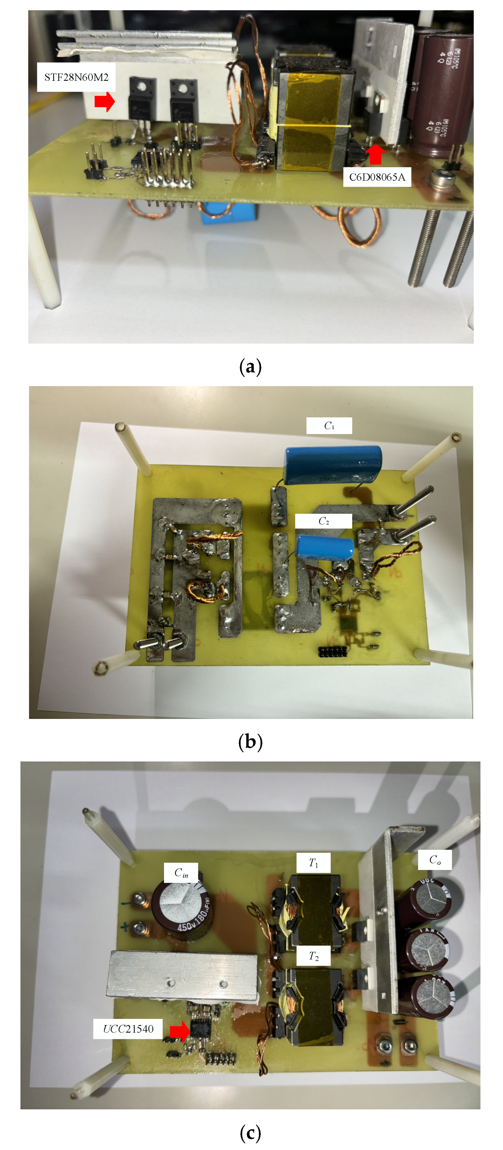
4. Experimental Results

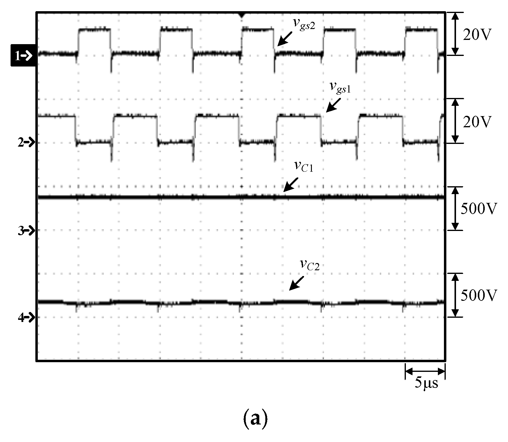
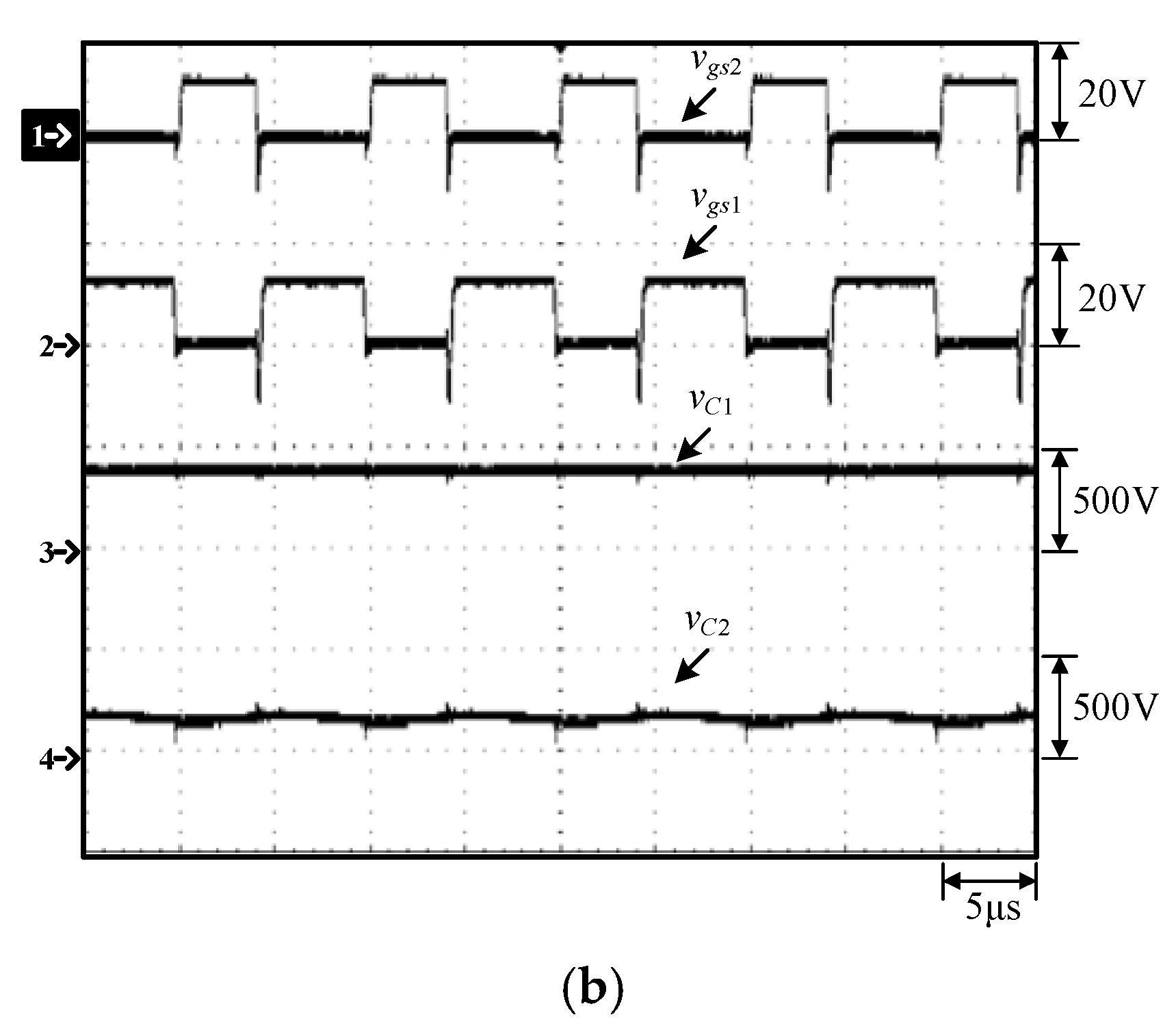
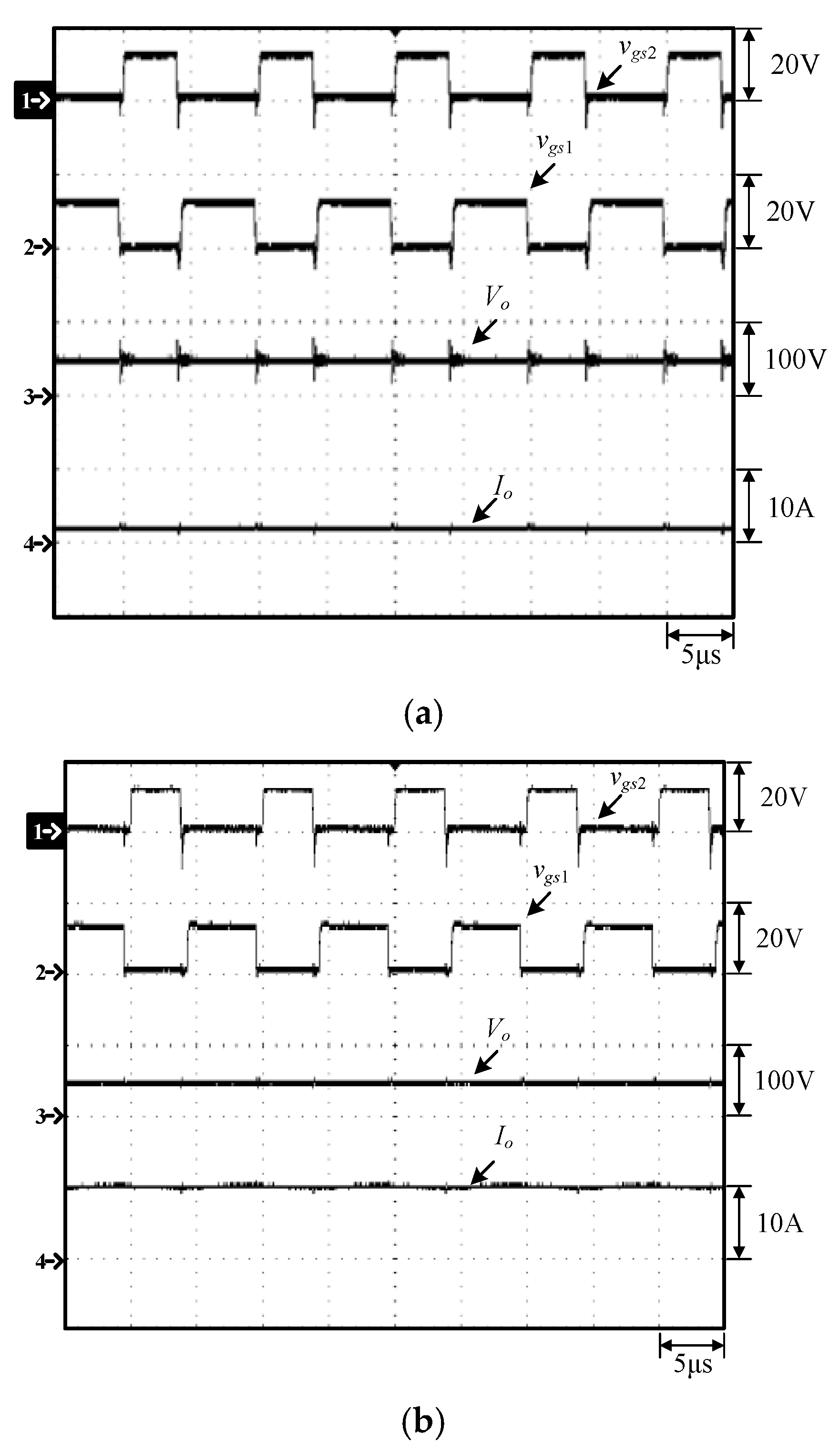
4.1. Measured Waveforms and Discussions

In this section, the experimental waveforms at the light and rated loads are presented to verify the design’s feasibility. Finally, the digital control will be realized by the FPGA to demonstrate its effectiveness. At light load, it can be seen that both the switches have ZVS turn-on for the main switch Q2 and the auxiliary switch Q1.
Figure 14 displays the gate driving signal vgs1 of the auxiliary switch Q1, the gate driving signal vgs2 of the main power switch Q2, the current ids1 of the auxiliary switch Q1, and the current ids2 of the main power switch Q2. Figure 15 displays the gate driving signal vgs1 of the auxiliary switch Q1, the gate driving signal vgs2 of the main switch Q2, the voltage vC1 of the clamping capacitor C1, and the voltage vC2 of the energy-transferring capacitor C2. Figure 16 displays the gate driving signal vgs1 of the auxiliary switch Q1, the gate driving signal vgs2 of the main switch Q2, the voltage vp1 on the primary side of the first transformer, and the voltage vp2 on the primary side of the second transformer. Figure 17 displays the gate driving signal vgs1 of the auxiliary switch Q1, the gate driving signal vgs2 of the main switch Q2, the output voltage Vo, and the output current Io. Figure 18 displays in the zoom-in gate driving signal vgs1 of the auxiliary switch Q1 and the voltage vds1 of the auxiliary switch Q1. Figure 19 displays the zoom-in gate driving signal vgs2 of the main switch Q2 and the voltage vds2 of the main switch Q2. Figure 20 displays a curve of efficiency versus load. Figure 21 shows the experimental setup.
Figure 14 shows that the currents in the two switches have negative currents, so the two switches Q1 and Q2 have ZVS turn-on, as shown in Figure 18 and Figure 19. Figure 16 displays that the magnetizing inductances Lm1 and Lm2 have voltage second balance. Figure 17 shows that the output voltage Vo is about 48 V and Io is about 2 A and 10 A, corresponding to the system specifications. Figure 20 displays the efficiency curve, which is up to 94.5% over all the load range; the maximum efficiency is about 96.4% at around half load, and the rated-load efficiency is about 94.5%.

4.2. Comparison Between Proposed and Other Topologies

Comparisons of the proposed converter with the existing active-clamp ZVS DC/DC converters [14,15,16,17,18,19] in various items are tabulated in Table 2. From this table, only the proposed converter has the highest efficiency.

5. Conclusions

A dual-transformer active-clamp is developed herein, where the two active clamping circuits utilize the same clamping capacitor to recycle the leakage inductance energy, and two resonant loops cause the main switch and the auxiliary switch to have ZVS turn-on to minimize the switching loss. From the efficiency measurement, the efficiency is above 94.5% for all the load range.

Author Contributions

Conceptualization, P.-C.T.; methodology, P.-C.T. and K.-I.H.; software, Y.-L.C.; validation, Y.-L.C. and J.-J.S.; formal analysis, P.-C.T., Y.-L.C. and K.-I.H.; investigation, J.-J.S.; resources, K.-I.H.; data curation, P.-C.T., Y.-L.C. and J.-J.S.; writing—original draft preparation, K.-I.H.; writing—review and editing, K.-I.H.; visualization, P.-C.T. and Y.-L.C.; supervision, K.-I.H.; project administration, K.-I.H.; funding acquisition, K.-I.H. All authors have read and agreed to the published version of the manuscript.

Funding

This research was funded by the Ministry of Science and Technology, Taiwan under Grant Number NSTC 112-2221-E-027-015-MY2.

Data Availability Statement

The original contributions presented in this study are included in the article. Further inquiries can be directed to the corresponding author.

Conflicts of Interest

The authors declare no conflicts of interest.

References

  1. Ali, A.; Khan, S.A.; Khan, M.U.; Ali, H.; Mughal, M.R.; Praks, J. Design of modular power management and attitude control subsystems for a microsatellite. Int. J. Aerosp. Eng. 2018, 2018, 2515036. [Google Scholar] [CrossRef]
  2. Khan, S.A.; Ali, A.; Tahir, M.; Tao, Z. Efficient power conditioning: Enhancing electric supply for small satellite missions. Aerospace 2024, 11, 920. [Google Scholar] [CrossRef]
  3. Tabisz, W.A.; Lee, F.C. Zero-voltage-switching multi-resonant technique-a novel approach to improve performance of high frequency quasi-resonant converters. In Proceedings of the IEEE Power Electronics Specialists Conference, Kyoto, Japan, 11–14 April 1998; pp. 9–17. [Google Scholar]
  4. Jia, P.; Su, Z.; Shao, T.; Mei, Y. An isolated high step-up converter based on the active secondary-side quasi-resonant loops. IEEE Trans. Power Electron. 2022, 37, 659–673. [Google Scholar] [CrossRef]
  5. Akhlaghi, B.; Farzanehfard, H.; Thiruvady, D.; Faraji, R.; Shiri, F. ZVT interleaved high step-up converter for renewable energy systems. In Proceedings of the 14th Power Electronics, Drive Systems, and Technologies Conference (PEDSTC), Babol, Iran, 31 January–2 February 2023; pp. 1–6. [Google Scholar]
  6. Javed, U.; Veerachary, M. ZVT boost converter integrated with charging and discharging topologies. In Proceedings of the IEEE International Power and Renewable Energy Conference (IPRECON), Kollam, India, 24–26 September 2021; pp. 1–6. [Google Scholar]
  7. Rani, N.C.; Amuthan, N. THD minimization of ZVT-ZCT quasi resonant SEPIC converter with proposed Harris Hawks optimization technique. In Proceedings of the 10th International Conference on Computing for Sustainable Global Development (INDIACom), New Delhi, India, 15–17 March 2023; pp. 1149–1154. [Google Scholar]
  8. Bodur, H.; Yıldırmaz, S. A new ZVT snubber cell for PWM-CCM boost converters. In Proceedings of the 25th European Conference on Power Electronics and Applications (EPE’23 ECCE Europe), Aalborg, Denmark, 4–8 September 2023; pp. 1–6. [Google Scholar]
  9. Guo, Y.L.; Chen, X.Y.; Sun, Z.; You, X. Analytical dVCE/dt model of high-power trench gate/field-stop IGBT modules considering dynamical conduction current at near-ZCT transient. IEEE J. Emerg. Sel. Top. Power Electron. 2024, 12, 4993–5003. [Google Scholar]
  10. Yau, Y.-T.; Hwu, K.-I.; Shieh, J.-J. Simple structure of soft switching for boost converter. Energies 2020, 13, 5448. [Google Scholar] [CrossRef]
  11. Hwu, K.-I.; Shieh, J.-J.; Jiang, W.-Z. Interleaved boost converter with ZVT-ZCT for main switches and ZCS for auxiliary switch. Appl. Sci. 2020, 10, 2033. [Google Scholar] [CrossRef]
  12. Hwu, K.-I.; Lin, Z.-F.; Tseng, P.-C. Boost converter with main switch possessing ZVT and ZCT and auxiliary switch possessing ZCS. Energies 2023, 16, 5504. [Google Scholar] [CrossRef]
  13. Wang, L.; Li, H.; Li, S. Burst mode control of active-power-decoupling integrated active clamp flyback PFC rectifiers. IEEE Trans. Power Electron. 2023, 38, 6337–6350. [Google Scholar] [CrossRef]
  14. Tang, C.-Y.; Lin, W.-Z.; Tan, Y.-C. An active clamp flyback converter with high precision primary-side regulation strategy. IEEE Trans. Power Electron. 2022, 37, 10281–10289. [Google Scholar] [CrossRef]
  15. Yan, Y.; Wang, T.; Wang, Y.; Zhu, M.; Tang, H.; Qian, Q. Adaptive dead-time and partial-ZVS regulation for GaN-based active clamp flyback converter with predictive hysteresis current mode control. IEEE Trans. Power Electron. 2023, 38, 10782–10797. [Google Scholar] [CrossRef]
  16. Rao, B.T.; De, D. A coupled inductor-based high-gain ZVS DC–DC converter with reduced voltage stresses. IEEE Trans. Power Electron. 2023, 38, 15956–15967. [Google Scholar] [CrossRef]
  17. Lin, J.-Y.; Chen, C.-T.; Lin, Y.-F. A novel hybrid cascaded and stacked coupled inductor boost converter with active clamping zero-voltage switching. IEEE Access 2025, 13, 608–617. [Google Scholar] [CrossRef]
  18. Wu, T.-F.; Lai, Y.-S.; Hung, J.-C.; Chen, Y.-M. Boost converter with coupled inductors and buck–boost type of active clamp. IEEE Trans. Ind. Electron. 2023, 55, 154–162. [Google Scholar] [CrossRef]
  19. Li, H.; Liu, M.; Yang, Y.; Song, Z.; Wang, Y. A multi-MHz active clamp topology for high cost-performance wireless power transfer. IEEE Trans. Power Electron. 2022, 37, 12828–12840. [Google Scholar] [CrossRef]
  20. Yau, Y.-T.; Hung, T.-L. A flyback converter with novel active dissipative snubber. IEEE Access 2022, 10, 108145–108158. [Google Scholar] [CrossRef]
Figure 1. Proposed active-clamp dual-transformer ZVS flyback converter.
Energies 18 03331 g001
Figure 2. Illustrated waveforms relevant to the proposed circuit.
Energies 18 03331 g002
Figure 3. Current flow in state 1.
Energies 18 03331 g003
Figure 4. Current flow in state 2.
Energies 18 03331 g004
Figure 5. Equivalent s-domain circuit diagram of the first resonant tank in state 2.
Energies 18 03331 g005
Figure 6. Equivalent s-domain circuit diagram of the second resonant tank in state 2.
Energies 18 03331 g006
Figure 7. Current flow in state 3.
Energies 18 03331 g007
Figure 8. Equivalent s-domain circuit diagram of the first resonant tank in state 3.
Energies 18 03331 g008
Figure 9. Equivalent s-domain circuit diagram of the second resonant tank in state 3.
Energies 18 03331 g009
Figure 10. Current flow state 4.
Energies 18 03331 g010
Figure 11. Equivalent s-domain circuit diagram of the first resonant tank in state 4.
Energies 18 03331 g011
Figure 12. Equivalent s-domain circuit diagram of the second resonant tank in state 4.
Energies 18 03331 g012
Figure 13. Block diagram of the proposed system configuration.
Energies 18 03331 g013
Figure 14. Measured waveforms at (a) light load and (b) rated load: (1) vgs2; (2) vgs1; (3) ids2; (4) ids1.
Energies 18 03331 g014
Figure 15. Measured waveforms at (a) light load and (b) rated load: (1) vgs2; (2) vgs1; (3) vC1; (4) vC2.
Energies 18 03331 g015aEnergies 18 03331 g015b
Figure 16. Measured waveforms at (a) light load and (b) rated load: (1) vgs2; (2) vgs1; (3) vp2; (4) vp1.
Energies 18 03331 g016
Figure 17. Measured waveforms at (a) light load and (b) rated load: (1) vgs2; (2) vgs1; (3) Vo; (4) Io.
Energies 18 03331 g017
Figure 18. Measured zoom-in waveforms at (a) light load and (b) rated load: (1) vgs1; (2) vds1.
Energies 18 03331 g018aEnergies 18 03331 g018b
Figure 19. Measured zoom-in waveforms at (a) light load and (b) rated load: (1) vgs2; (2) vds2.
Energies 18 03331 g019
Figure 20. Curve of efficiency versus load current.
Energies 18 03331 g020
Figure 21. Experimental setup: (a) input side; (b) bottom side; (c) output side.
Energies 18 03331 g021
Table 1. System specifications.
Input Voltage (Vin)380 V
Output Voltage (Vo)48 V
Rated Output Power (Po,rated)500 W
Minimum Output Power (Po,min)100 W
Switching Frequency (fs)100 kHz
Maximum Duty Cycle of Main Switch (Dmax)0.4
Table 2. Comparisons between the proposed converter and existing active-clamp ZVS DC/DC converters.
[14][15][16][17][18][19]Proposed
Rated-load Power (W)10065250400200120500
Input Voltage (V)400150304030250380
Output Voltage (V)4819.53604002004848
Voltage Gain D n ( 1 D ) D n ( 1 D ) 2 + 3 n n D ( 1 D ) 2 2 n D + 1 1 D n D + 1 1 D --- D n
Switching Frequency (kHz)10060070100661000100
No. of SwitchesMOSFET (2)GaN (2) + MOSFET (1)MOSFET (2)MOSFET (2)MOSFET (2)MOSFET (2)MOSFET (2)
No. of Transformers (Coupled Inductors)1(0)1(0)1(2)0(2)0(2)1(0)2(0)
No. of Capacitors1153132
No. of Diodes1052142
Maximum Efficiency (%)---93.7496.194.692.092.496.4
Control StrategyPSRSPHCMPWMPWMPWMPWMPWM
Isolationvvxxxvv
Disclaimer/Publisher’s Note: The statements, opinions and data contained in all publications are solely those of the individual author(s) and contributor(s) and not of MDPI and/or the editor(s). MDPI and/or the editor(s) disclaim responsibility for any injury to people or property resulting from any ideas, methods, instructions or products referred to in the content.

