Article

Series Resonant LED Driver with Current Equalization Based on the Differential-Mode Transformer

by
Kuo-Ing Hwu
* and
Jun-Yi Lee
Department of Electrical Engineering, National Taipei University of Technology, 1, Sec. 3, Zhongxiao E. Rd., Taipei 10608, Taiwan
*
Author to whom correspondence should be addressed.
Energies 2025, 18(12), 3071; https://doi.org/10.3390/en18123071
Submission received: 25 April 2025 / Revised: 7 June 2025 / Accepted: 9 June 2025 / Published: 10 June 2025

Abstract

In this research, a series resonant LED driver circuit based on the differential-mode transformer for current equalization is proposed. In this circuit, the series resonant converter adopts controlled frequency modulation to change the energy transferred to the output while realizing zero voltage switching (ZVS) turn-on of the half-bridge switch. To deal with the problem of unequal LED currents caused by two different forward conduction voltages of the output LED strings, a differential-mode transformer is employed to balance the currents between the two LED strings, and the relationship between the magnetizing inductance and the percentage of current sharing error are derived to facilitate the design. Furthermore, only the current of one LED string needs to be sensed to achieve current equalization, while the current of the other LED string is automatically determined by the differential-mode transformer.

1. Introduction

1.1. LED Future

The invention of light emitting diodes (LEDs) and the advancement of power supplies have led to improving lighting systems, replacing the inconveniences of traditional lamps [1]. Since the LED driver is designed to supply a fixed current to power LED strings [2], the current equalization control is required to solve the problem of current imbalance between the LED strings.

1.2. LED Current Equalization

The LED current equalization can be categorized into two types: active and passive.

1.3. Active Type

For the active current equalization method, it can be divided into two types: linear and switching. Generally speaking, the linear regulator is the switch operated in the linear region and can be regarded as the variable resistor [3]. In order to achieve the LED current balance, the literature [4] proposes an adaptive voltage circuit between the main power stage and the LED strings, so that the voltage across the switch of the linear regulator can be regulated to reduce the loss of energy. Another active current equalization method is to add an additional switching converter to achieve current equalization by switching. The studies [5,6] present experiments in which each string of LEDs is connected to the corresponding converter, and the output current of the converter is used to achieve current equalization of each string of LEDs. In the LED driver proposed in [7,8,9], a dimming switch is added to each LED string, and the duty cycle of the pulse width modulated (PWM) signal is adjusted to change the average value of current flowing through the LED string to achieve current equalization.

1.4. Passive Type Without Soft Switching

Passive methods utilize the characteristics of passive components to achieve current equalization, and are divided into capacitor current equalization and transformer current equalization. The capacitor equalization method mentioned in [10] is when two different LED series have a voltage difference; the current equalization capacitor for charging and discharging is added, because the capacitor in the steady state has the characteristics of the ampere-second balance. The literature [11] shows a two-channel interleaved step-down LED driver using current equalization capacitors. In this circuit, the energy of the previous stage is transferred to the next LED driver through the current equalization capacitor, and thus part of the energy is consumed in the process of the transfer, which leads to relatively large current errors between the LEDs in the later stages. The transformer current equalization method can also be a method used for the current equalization of LED strings through the same turns of the transformer windings, and the primary and secondary sides of the transformer will be connected with two different LED strings. When the voltage of the LED string is unbalanced, a differential-mode signal will be generated on the transformer, and the current equalization transformer will be activated to force the currents through the LED strings to be identical by utilizing the characteristics of the same number of turns on the primary and secondary sides. The current equalization circuit using a differential-mode transformer proposed in the literature [12,13] must add a freewheeling diode or a zener diode to each LED string to ensure that the differential-mode transformer has sufficient demagnetization voltage to make the switch completely demagnetized during the switch cutoff period, so the duty cycle of the switch will be limited.

1.5. Passive Type with Soft Switching

Today’s high power density LED driver circuits require switching power supplies to cope with the increased demand for LED loads. Although increasing the switching frequency of the switches can reduce the size of the passive components, the problems of switching loss and electromagnetic interference (EMI) become more serious with hard switching. In order to solve the above problems, the soft switching technology has been developed, which can be divided into zero voltage switching (ZVS) and zero current switching (ZCS), which can reduce the cross area between current and voltage during the switching period to minimize the switching loss. The literature [14] proposes a two-stage multi-channel LED driver; the front stage is a buck converter to regulate the rear-stage CLL resonant converter, so that the latter can be operated at the resonant frequency through the primary-side coils of the transformers in series connection to achieve current equalization between the LED string modules, and in each LED string, a current equalization capacitor is added to balance the LED string module current flow in the opposite direction of the two LED strings. The literature [15] proposes a step-down converter without any transformer, which operates in DCM mode with ZCS. At the same time, the amperage-second balance of the resonant capacitor is utilized to achieve the current equalization between the LED strings. In comparison, the difference between [15,16] is that the resonant current is operated in CCM and DCM, respectively, and the switch achieves ZVS turn-on when operated in CCM and ZCS turn-off when operated in DCM. The literature [17] proposes an LED driver that combines an LLC resonant converter and a current balancing circuit. A half-bridge LLC converter is employed to provide the primary-side switches’ ZVS turn-on and the secondary-side rectifier diodes’ ZCS turn-off, and a current equalization capacitor is added to the secondary side to balance the current flowing through the LED strings. The literature [18] proposes an LCLC resonant LED driver, where the resonant tank of the LCLC can provide a relatively large ZVS range to the switch, and at the same time reduce the current stress of the switch, and finally achieve the LED current regulation through the auxiliary switch. However, because the number of resonant components in this circuit is relatively large, there are several resonance points, causing the control of the range of operating frequency to be designed carefully. In addition to the original resonant topology, the ZCS turn-off is applied to an additional auxiliary resonant circuit or snubber. The literature [19] adopts an interleaved buck-boost structure, consisting of two phases, and adds one coupling inductor to replace the original two inductors, which are resonated with the parasitic capacitance of the main switch to realize the ZVS turn-on of the switch. In [20], a passive damping circuit is added to reduce the overlapping area of switching voltage and current during the switching period, so many passive components and diodes are added, resulting in additional losses. In addition, the auxiliary inductors in the damping circuit oscillate with the parasitic components of the switch during the switch cutoff period, resulting in additional switching losses. In [21], a dimmable LED driver based on H-bridge and differential-mode transformer are presented.

1.6. Purpose of This Research

In this research, the purpose of this paper is to improve the magnetic resetting of the differential-mode transformer. Compared with [12,13], the circuit proposed in this paper is not limited by the duty cycle of the gate driving signals for the main switches, so a higher load regulation range can be achieved. In this circuit, the resonant circuit enables the half-bridge switch to realize ZVS turn-on.

1.7. Contents of This Paper

There are seven sections in this paper. Section 1 talks about the introduction, Section 2 will introduce the system configuration, Section 3 will describe the operating principle, Section 4 will show design considerations, Section 5 will give the experimental results, Section 6 will give the literature comparison, and, finally, the conclusion will be made.

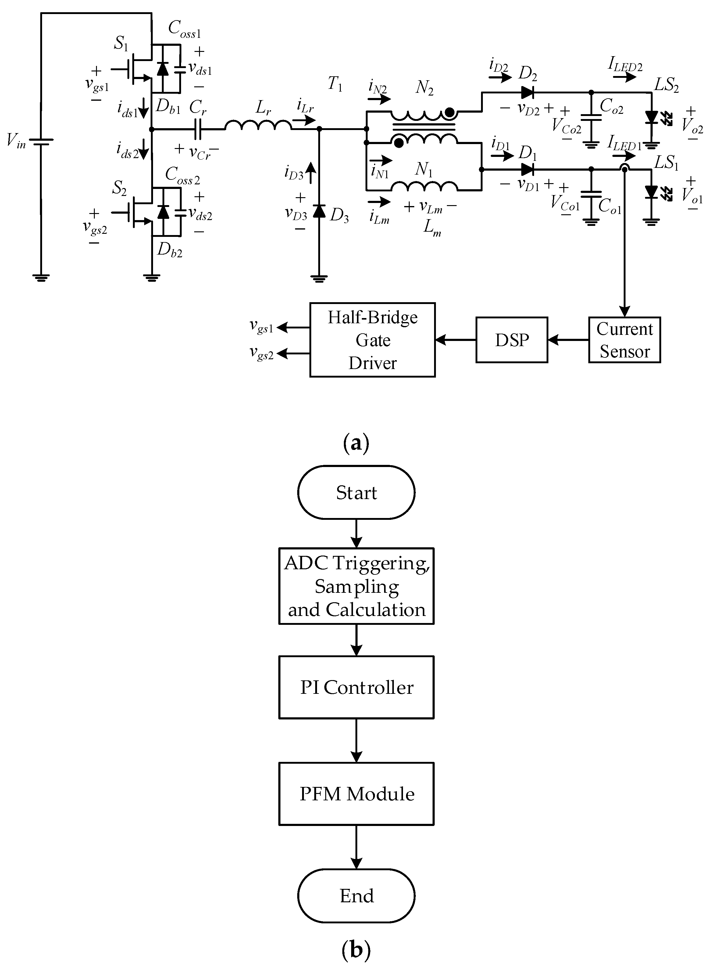
2. System Configuration

Figure 1 shows the series resonant LED driver circuit based on the differential-mode transformer current equalization; the main structure uses a half-bridge series resonant converter. The feedback circuit uses a current sensor to obtain the current feedback signal from one of the LED strings, which is sent to the analog-to-digital converter (ADC) inside the DSP. Afterwards, this sensed feedback signal is subtracted from the current reference to obtain the corresponding error signal through the DSP algorithm calculation. After this, the corresponding control force can be obtained, and finally the control force is transferred to variable frequency and sent to the half-bridge switches S1 and S2 through an isolated half-bridge gate driver to control these two switches.
As shown in Figure 1a, the circuit consists of two switches S1 and S2, a resonant inductor Lr and a resonant capacitor Cr formed by the series resonant tank, with the function of current equalization based on differential-mode transformer T1, which is composed of a magnetizing inductor Lm, a primary-side coil N1, a secondary-side coil N2, the primary-side and secondary-side leakage inductances Llk1 and Llk2, respectively, the two rectifier diodes D1 and D2, and the freewheeling diode D3. In addition, the load side is composed of two LED strings LS1 and LS2, and two output capacitors Co1 and Co2.
As for the DSP algorithm, it is described in Figure 1b, showing the program flow diagram of the system operation, which is composed of three main sub-modules, namely, the ADC triggering, sampling and calculation; the proportional and integral (PI) controller; and the pulse frequency modulation (PFM) module. Firstly, the analog feedback signal is sampled by triggering the ADC to create a digital value. Then, this digital value is subtracted from the set reference value to get an error. This error is then fed into the PI module to generate the corresponding control force, and then the PFM module is used to send out the signal to regulate the switch.

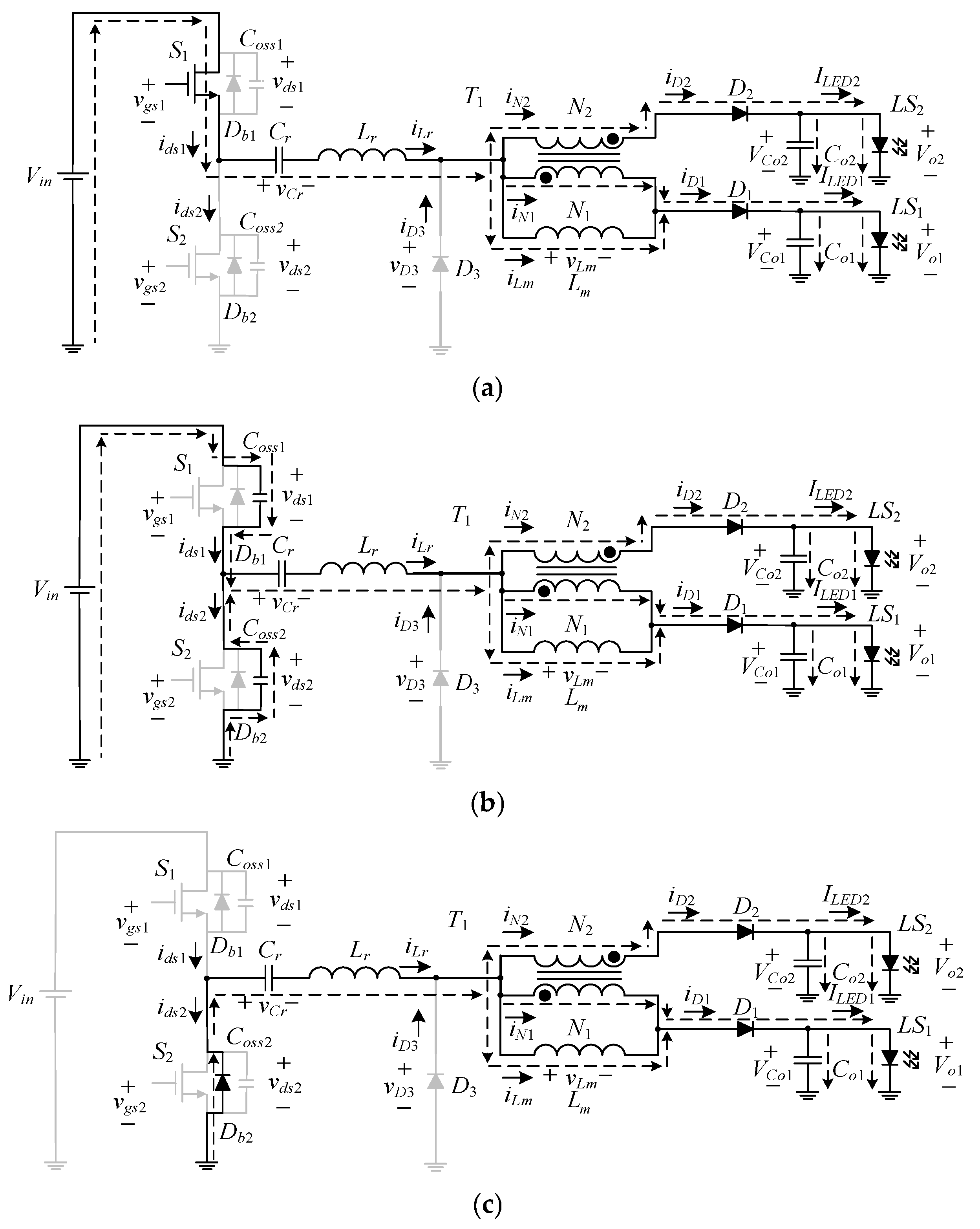
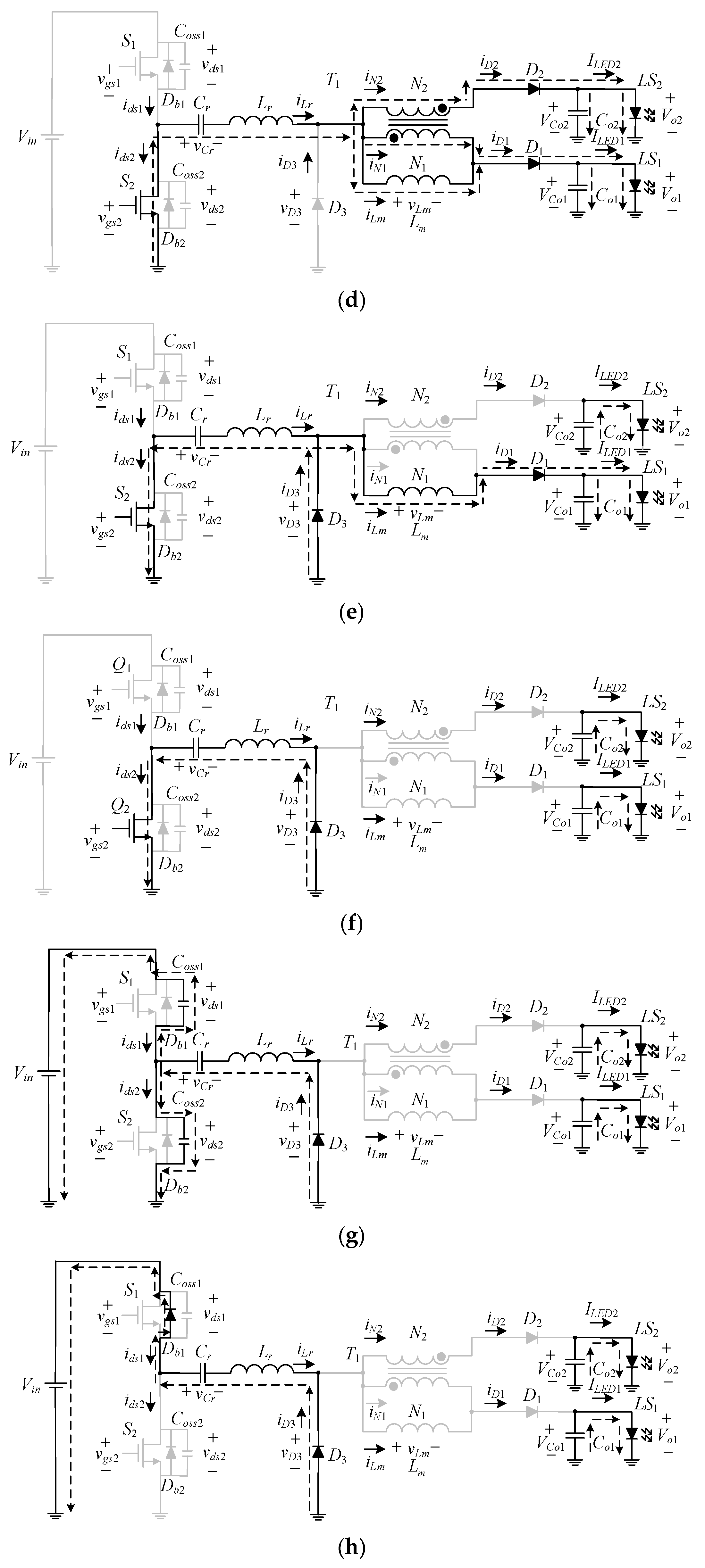
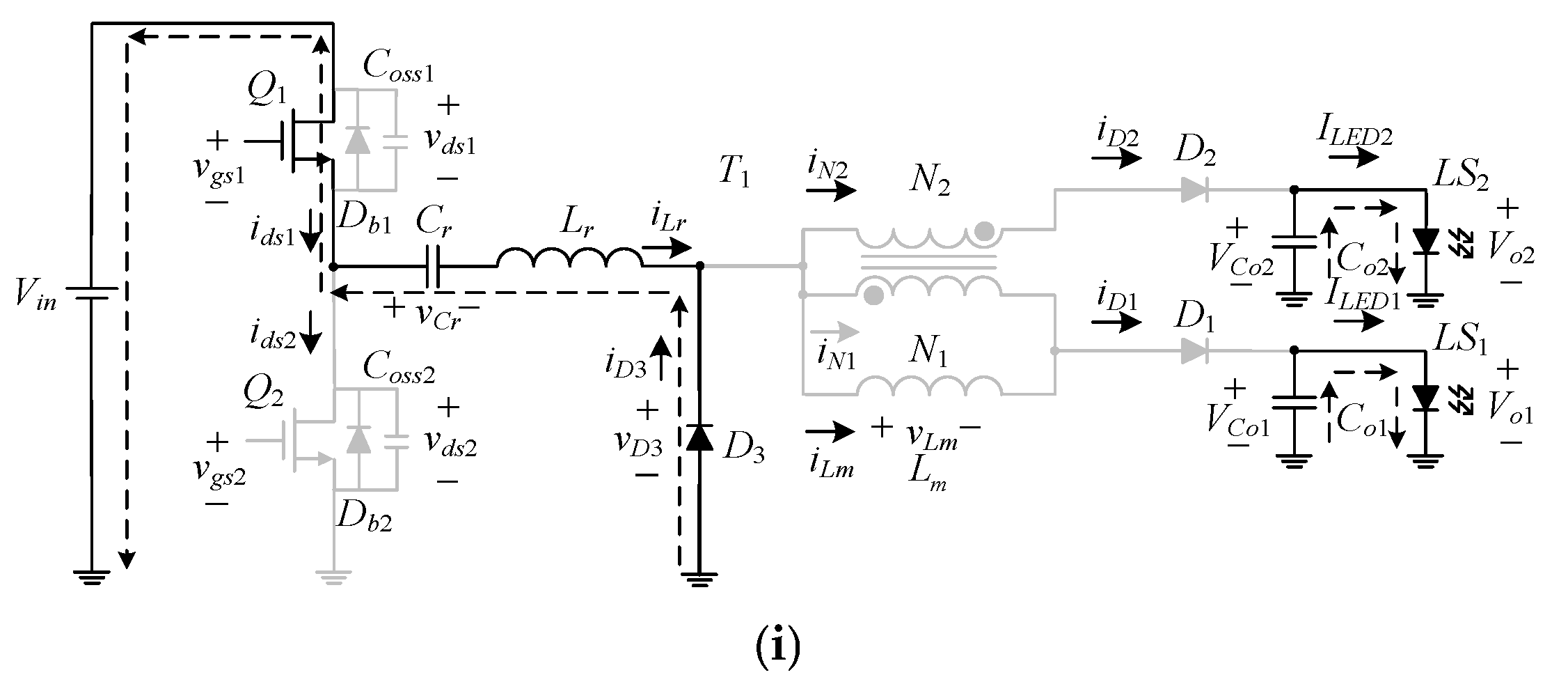
3. Operating Principle

Before introducing the analysis of the circuit behavior, there are some assumptions and symbol definitions:
(1)
Vin is the input voltage; LS1 and LS2 are the output LED strings and the voltages on them are equal to the output voltages Vo1 and Vo2, respectively.
(2)
S1 and S2 are the switches of the upper and lower switches of the half-bridge, Db1 and Db2 are the body diodes of the switches S1 and S2, respectively, Coss1 and Coss2 are the output capacitances of the switches S1 and S2, respectively, and the corresponding forward conduction voltages are assumed to be zero.
(3)
The characteristics of rectifier diodes D1 and D2 and magnetic resetting diode D3 are ideal.
(4)
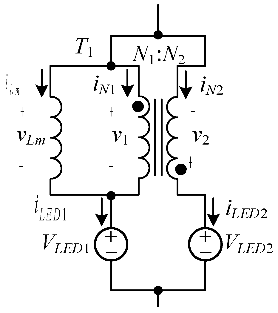
The coupling coefficient of the differential-mode transformer is one, i.e., only the magnetizing inductance Lm is taken into account, and the leakage inductances Llk1 and Llk2 are ignored.
(5)
The output capacitors Co1 and Co2 are large enough to be considered as constant.
(6)
The current through the resonant inductor Lr is iLr, and the voltage on the resonant capacitor Cr is vCr.
(7)
vds1 is the voltage on the switch S1, vds2 is the voltage on the switch S2, vD1 is the voltage on the diode D1, vD2 is the voltage on the diode D2, vD3 is the voltage on the diode D3, and vLm is the voltage on the magnetizing inductance Lm.
(8)
ids1 is the current flowing through the switch S1, ids2 is the current flowing through the switch S2, iD1 is the current flowing through the diode D1, iD2 is the current flowing through the diode D2, iD3 is the current flowing through the diode D3, iN1 is the primary-side current of the differential-mode transformer T1, iN2 is the secondary-side current of the differential-mode transformer, iLm is the current flowing through the magnetizing inductance Lm, ILED1 is the current flowing through the first LED string LS1, and ILED2 is the current through the second LED string LS2.
(9)
vgs1 and vgs2 are the driving signals for the upper arm of switches S1 and S2, respectively.
(10)
Ts is the switching period, and fs is the switching frequency.
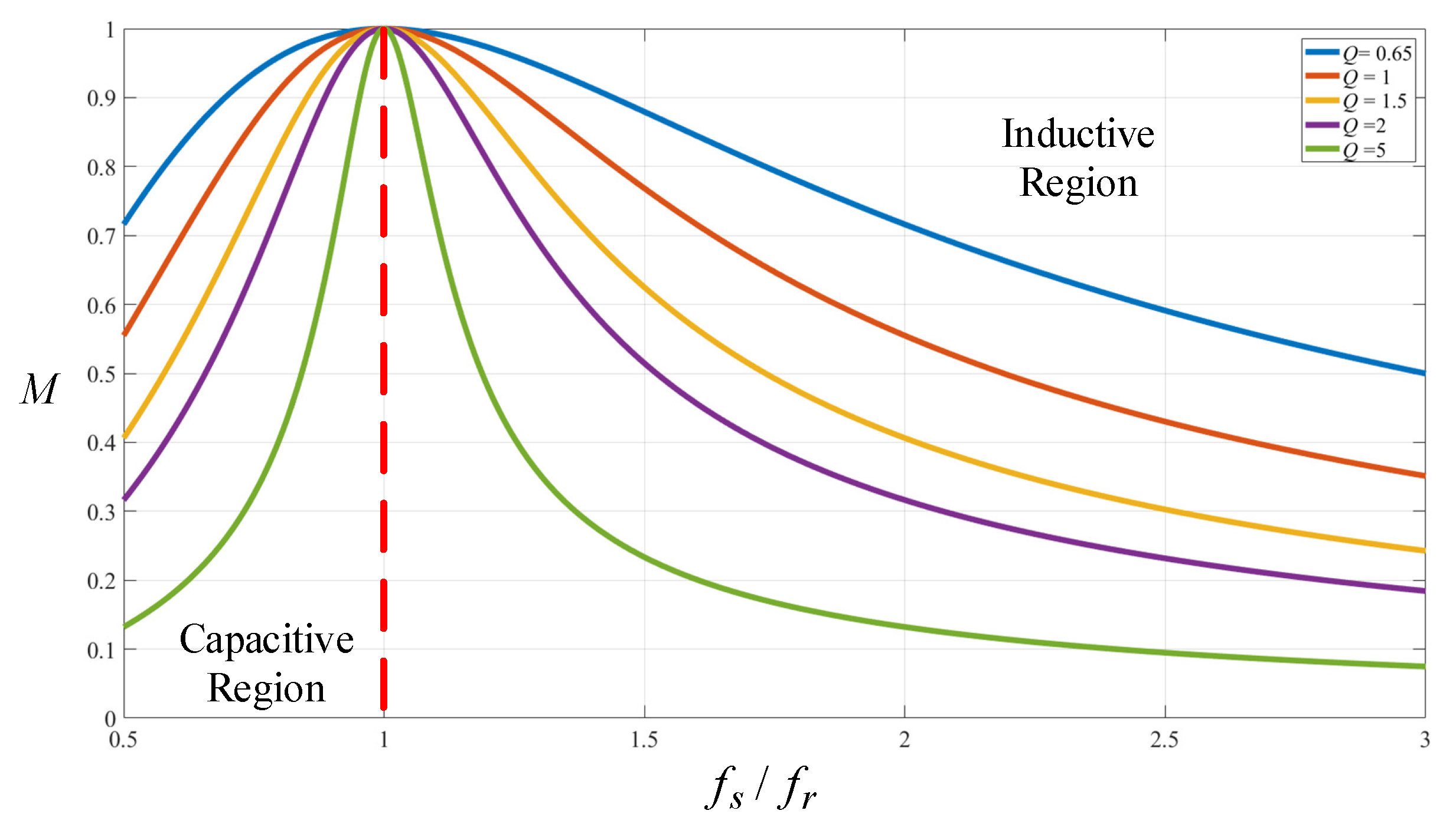
Figure 2 shows key waveforms relevant to the proposed circuit.
State 1. [ t 0 t < t 1 ] : As shown in Figure 3a, the switch S1 is on, the switch S2 is off, and the resonant inductor current iLr resonates from negative to zero. Sequentially, the resonant inductor Lr and the resonant capacitor Cr resonate with each other, and the resonant inductor current iLr starts to flow positively from zero. The current flows from the input Vin, through the switch S1, the resonant capacitor Cr, the resonant inductor Lr, the diodes D1 and D2, and the differential-mode transformer T1 to the LED strings LS1 and LS2. If there is a voltage difference between the two LED strings, the differential-mode transformer is activated, and the voltage on Lm, called vLm, is clamped at half of the difference in voltage between the two LED strings, and the magnetizing inductance Lm starts to be linearly excited. Once the switch S1 cuts off, the circuit enters state 2.
State 2. [ t 1 t < t 2 ] : As shown in Figure 3b, the switches S1 and S2 are off. During this state, the resonant inductor current iLr still flows positively, and the current flows to the LED strings LS1 and LS2 through the differential-mode transformer T1 and the freewheeling diodes D1 and D2. In this state, the operation of the differential-mode transformer T1 and the two LED strings LS1 and LS2 is the same as that in the previous state. Since both of the switches are in the off-state and the resonant current iLr must continue, the resonant inductor current iLr is the same as that in the previous state. The resonant inductor current iLr charges the output capacitor Coss1 of the switch S1 and discharges the output capacitor Coss2 of the switch S2, respectively. The moment the output Coss1 is charged to the input voltage Vin and the output Coss2 is discharged to zero, the circuit enters state 3.
State 3. [ t 2 t < t 3 ] : As shown in Figure 3c, the switches S1 and S2 are still cut off. During this state, the output capacitor Coss2 of the switch S2 has been discharged to zero, causing the body diode Db2 of the switch 0S2 to conduct, and the resonant inductor current iLr is still positively flowing and gradually decreasing. In this state, the differential-mode transformer T1 and the two LED series LS1 and LS2 operate as in the previous state. Once the switch S2 is turned on, the circuit enters state 4.
State 4. [ t 3 t < t 4 ] : As shown in Figure 3d, the switch S1 is still off and the switch S2 is on. During this state, since the body diode of S2 was first conducted in the previous state, the voltages across the switches S1 and S2 are close to zero, so the switch S2 is turned with ZVS. In addition, the resonant inductor current iLr flows in the positive direction and decreases gradually. In this state, the differential-mode transformer T1 and the LED strings LS1 and LS2 operate as in the previous state. As soon as the resonant inductor current iLr decreases to zero, the circuit enters state 5.
State 5. [ t 4 t < t 5 ] : As shown in Figure 3e, the switch S1 remains off and the switch S2 remains on. During this state, the resonant inductor current iLr starts to flow from zero in the opposite direction. In addition, the magnetizing inductor Lm of the differential-mode transformer T1 is demagnetized through the freewheeling diode D1 and the magnetic resetting diode D3, so the magnetizing inductance current iLm decreases linearly. Note that this experienced time in this state is much smaller than half of the switching period. Once the magnetizing inductance current iLm drops to zero, the circuit proceeds to state 6.
State 6. [ t 5 t < t 6 ] : As shown in Figure 3f, the switch S1 is still off and the switch S2 is continuously on. During this state, the resonant inductor current iLr flows negatively through the diode D3. In addition, since the magnetizing inductor current iLm has been demagnetized to zero, the freewheeling diodes D1 and D2 are both cut off and there is no energy sent to the output side. Therefore, the energy required for the LED strings LS1 and LS2 is supplied by the output capacitors Co1 and Co2, respectively. The moment the switch S2 is cut off, the circuit enters state 7.
State 7. [ t 6 t < t 7 ] : As shown in Figure 3g, the switches S1 and S2 are cut off. During this state, the resonant inductor current iLr still flows negatively through D3, and the freewheeling diodes D1 and D2 are still cut off. In addition, the operation of the differential-mode transformer T1 and the output is the same as the previous state. Since the switches S1 and S2 are off, the resonant inductor current iLr discharges Coss1 and charges Coss2. As soon as the output capacitance Coss1 discharges to zero and the output capacitance Coss2 charges to Vin, the circuit enters state 8.
State 8. [ t 7 t < t 8 ] : As shown in Figure 3h, the switches S1 and S2 are in the off-state. During this state, since the output capacitor Coss1 of the switch S1 has been discharged to zero, the body diode Db1 of the switch is on, and the resonant inductor current iLr flows through the diode D3, the resonant inductor Lr, the resonant capacitor Cr, the body diode Db1 of the switch S1, and the input. In addition, the differential-mode transformer and the two LED strings LS1 and LS2 operate in the same way as in the previous state. Once the upper arm switch S1 turns on, the circuit enters state 9.
State 9. [ t 8 t < t 0 + T s ] : As shown in Figure 3i, the switches S1 is on and the switch S2 is off. During this state, since the body diode Db1 of the switch has been on in the previous state, the switch S1 can realize ZVS turn-on, and the resonant inductor current iLr flows negatively and rises continuously. In addition, the differential-mode transformer and the two LED series LS1 and LS2 operate as in the previous state. The moment the resonant inductor current iLr rises to zero, the circuit proceeds to the next cycle.

Voltage Gain

The first harmonic approximation (FHA) is utilized herein to find the equivalent output AC load resistance Ro,ac, reflected from the secondary side to the primary side, to be derived as follows.
First, the average value ILr,avg of the half-cycle resonant current iLr is the sum of the currents in the two LED strings, equal to the total output current Io:
I L r , a v g = I L E D 1 + I L E D 2 = I o
Also, the peak value ILr,peak and RMS value IL,rms of the resonant current iLr can be expressed as follows:
I L r , p e a k = I o × π
I L r , r m s = I L r , p e a k × 1 2 = π × I o 2
The output voltage vo of the resonant tank is the voltage on the diode D3, which is a unipolar square wave, that is,
v o ( t ) = v D 3 ( t ) = V o ,   i L r ( t ) > 0 v o ( t ) = v D 3 ( t ) = 0   ,   i L r ( t ) < 0
Thus, the fundamental RMS value Vo,FHA,rms of the output voltage vo of the resonant tank is
V o , F H A , r m s = 2 × V o π
Eventually, dividing Equation (5) by Equation (3) yields
R o , a c = V o , F H A , r m s I L r , r m s = 2   ×   V o π π   ×   I o 2 = 2 π 2 V o I o = 2 R o π 2
On the other hand, the input voltage vin of the resonant can be expressed as
v i n ( t ) = v d s 2 ( t ) = V i n , 0 t T s 2 v i n ( t ) = v d s 2 ( t ) = 0 , T s 2 t T s
Therefore, the RMS value of the fundamental wave of vin is
V i n , F H A , r m s = 2 V i n π × 1 2 = 2 π V i n
From the above derivation, the relationship between the input fundamental waveform and the output fundamental waveform of the resonant tank can be found. By using Equations (5) and (8), the DC gain Mdc of the circuit can be expressed by
M d c = V o , F H A , r m s V i n , F H A , r m s = 2   ×   V o π 2   ×   V i n π = V o V i n
According to Equations (3), (5), and (8), the s-domain equivalent circuit of the proposed circuit is shown in Figure 4.
According to Figure 4, the voltage gain M(s) of the circuit is given by
M ( s ) = V o , F H A ( s ) V i n , F H A ( s ) = R o , a c s L r + 1 s C r + R o , a c
The defined resonant radian frequency ωr, the characteristic impedance Zr, and the quality factor Q are
ω r = 1 L r C r ,   Z r = L r C r ,   Q = Z r R o , a c
Substituting Equation (11) into Equation (10) yields
M ( s ) = s ω r × 1 Q ( s ω r ) 2 + s ω r 1 Q + 1
Substituting s = j ω s = j 2 π f s and ω r = j 2 π f r into Equation (10) and letting M = M ( j 2 π f s ) , the voltage gain M of the proposed circuit is given by
M = V o V i n = 1 Q 2 f r f s 2 + f s f r 2 2 + 1
Figure 5 shows the curve of voltage gain M versus the ratio of switching frequency fs to resonant frequency fr for different values of quality factor Q. In the case of fixed resonant elements, the smaller the load resistance is, the larger the value of Q is, the curve of the voltage gain M is steeper, and the voltage gain is more likely to be caused by the change in frequency, so the stability of the system is poorer but the response speed of voltage regulation is faster. On the contrary, the smaller the value of Q is, the larger the frequency change range is needed to stabilize the output voltage.
Figure 6 shows the current equalization circuit of the differential-mode transformer T1, where N1 and N2 are the primary and secondary windings of the differential-mode transformer T1 with N1 equal to N2, Lm is the primary-side magnetizing inductance, and LED1 and LED2 are the loads connected in series to N1 and N2, respectively. In addition, iN1 and iN2 are the primary-side and secondary-side currents of T1, respectively. iLm is the current flowing through the magnetizing inductance Lm, v1 and v2 are the primary-side and secondary-side voltages of T1, respectively, and vLm is the voltage on the magnetizing inductance Lm of T1.
Since the turns ratio is one and the polarity dots are in the opposite direction, the following are the results
v L m = v 1 = v 2
i N 1 = i N 2
In Figure 6, according to Kirchhoff’s voltage law, it can be known that
v 1 + V L E D 1 = v 2 + V L E D 2
When two LED strings have the same voltages on them, i.e., VLED1 = VLED2, according to Equations (14) and (16), there is no voltage on the differential-mode transformer T1, i.e., T1 is not activated. When a voltage imbalance occurs, a balancing voltage on the magnetizing inductance is generated, as shown in Equation (17). Accordingly, T1 is activated, forcing the primary and secondary sides of T1 to have the same currents, i.e., equalizing the currents in LED1 and LED2 due to the turns ratio of one.
v L m = V L E D 2 V L E D 1 2
However, in practice, there must be a magnetizing inductance Lm. Therefore, in the case of voltage imbalance, the balanced voltage will energize the magnetizing inductance and generate the magnetizing current iLm, and the average value of this current will be the current error between the two LED strings. In Figure 6, according to Kirchhoff’s current law, it can be seen that
i L E D 1 = i N 1 + i L m
i L E D 2 = i N 2
Accordingly, in the process of current equalization, the current in the magnetizing inductance Lm of T1, called iLm, will cause the current equalization error.
From Section 3, it can be seen that the magnetizing inductance Lm is linearly excited in states 1 to 4 ( t 0 t < t 4 ) and the voltage vLm is 0 . 5 × ( V o 1 V o 2 ) . In state 5, the magnetizing inductance Lm is linearly demagnetized, and the voltage vLm is V o 1 . Figure 7 shows the operating behavior of the magnetizing inductance.
Δ I o = Δ V 16 × L m × f s L m = Δ V 16 × f s × 2 × I L E D 1 1 ε 2 × I L E D 1
From Figure 7, the elapsed time of the magnetizing inductance Lm is 0.5Ts, and the magnetization voltage is much smaller than the demagnetization voltage. So, the demagnetization time can be ignored, and the average value of the magnetizing inductance current, called ILm,avg, can be expressed as
I L m ,   a v g = Δ I o = 1 T s ( 1 2 × Δ V 2 L m × 0.5 T s × 0.5 T s ) = Δ V 16 × L m × f s
where Δ V is the difference in voltage between the two LED strings, namely, V o 1 V o 2 .
After that, the average Iavg of the currents of the two LED strings can be expressed by
I a v g = I L E D 1 + I L E D 2 2
Substituting Equations (18) and (19) into Equation (22) yields
I a v g = I L E D 1 + I L E D 2 2 = I N 1 + Δ I o + I N 2 2 = 2 I L E D 1 Δ I o 2
Sequentially, the current sharing error percentage ε is defined to be
ε = I a v g I L E D 1 I a v g × 100 % = I a v g I L E D 2 I a v g × 100 %
By substituting Equation (23) into Equation (24), the current error Δ I o can be expressed as
Δ I o = 2 × I L E D 1 1 ε 2 × I L E D 1
By substituting Equation (25) into Equation (20), the relationship between the current error percentage and the magnetizing inductance Lm can be obtained to be
Δ I o = Δ V 16 × L m × f s L m = Δ V 16 × f s × 2 × I L E D 1 1 ε 2 × I L E D 1

4. Design Considerations

The system specifications of the proposed circuit are shown in Table 1.
Since the rated-load voltage of a single LED is about 3.2 V, the output rated voltage Vo,rated on an LED string is 32 V, which is constructed by the voltage of 10 LEDs in series. In the case of unbalanced output, the two LED strings are composed of 10 LEDs in series and 8 LEDs in series, respectively. The current error percentage between the two LED strings must be less than 1% from 25% to 100% of the load.
In this section, the parameters of the resonant tank, differential-mode transformer, and output capacitor will be designed.

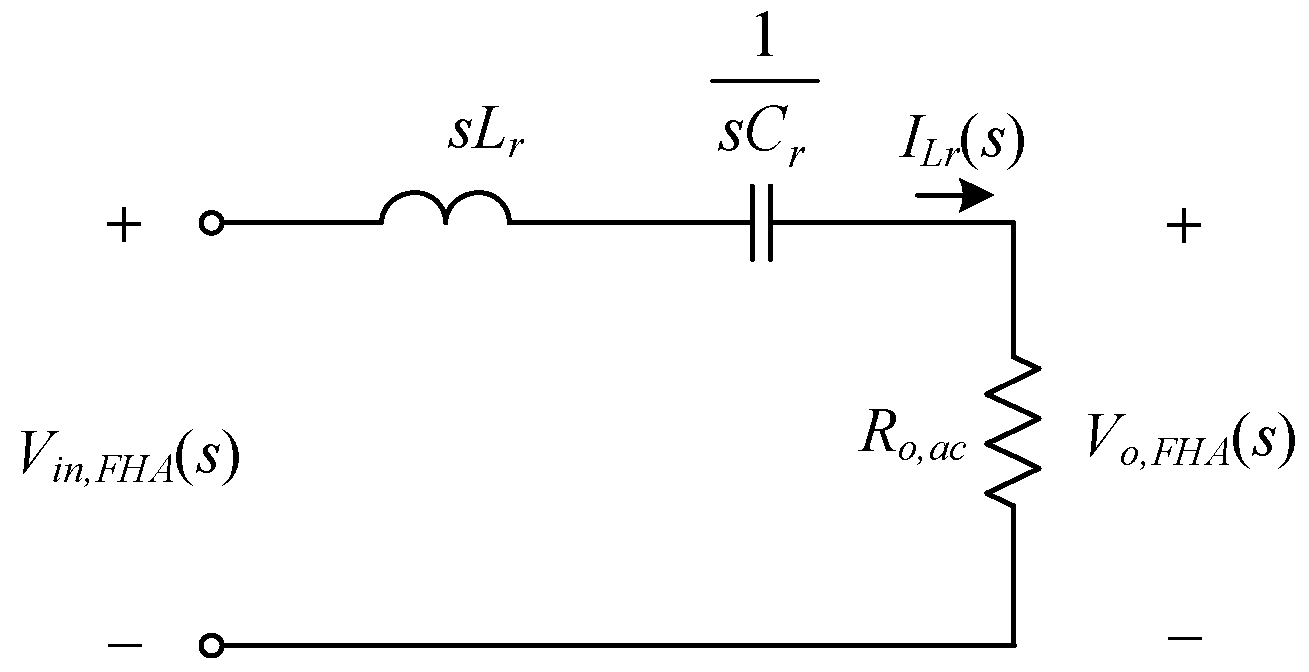
4.1. Equivalent Output AC Load Resistance Ro,ac

According to Table 1, the value of Ro is
R o = V o , r a t e d I o , r a t e d = 32 0.7 45.7 Ω
Therefore, the value of Ro,ac can be found according to Equation (6), that is,
R o , a c = 2 R o π 2 = 2 × 54.7 π 2 9.27 Ω

4.2. Resonant Components Lr and Cr

By considering the range of operating frequency and the stability of the system control, the value of Q is set at 2. By substituting the resonant frequency of 100 kHz in Table 1 into Equation (11), the value of the resonant capacitor Cr can be obtained first:
Q = 1 2 × π × f r × R o , a c × C r C r = 1 2 × π × f r × R o , a c × Q = 1 2 × π × 100 × 10 3 × 9.27 × 2 = 85.8 nF
Therefore, a plastic capacitor of 82 nF is selected and close to the calculated value. Afterwards, the value of the resonant capacitor Cr and the value of the resonant frequency fr are used to find the value of the resonant inductor Lr:
f r = 1 2 × π × L r × C r L r = 1 ( 2 × π × f r ) 2 × C r = 1 ( 2 × π × 100 × 10 3 ) × 82 × 10 9 = 30.92 μ H
Accordingly, the actual value of Q is 2.09 based on the selected elements of the resonant tank.

4.3. Magnetizing Inductance Lm

By using the simulation software PSIM 9.11, the voltages Vo1 and Vo2 of the two LEDs at 25% load are 28.98 V and 22.42 V, respectively. Meanwhile, the voltage gain M(25%) and quality factor Q(25%) at 25% load are as follows:
M ( 25 % ) = V o V i n = 28.98   +   22.42 2 48 = 0.54
Q ( 25 % ) = Z r R o . a c ( 25 % ) = 30.89   ×   10 6 82   ×   10 9 2   ×   25.74 π 2   ×   0.7   ×   0.25 = 0.65
where Vo is the average voltage of the voltages on the two LED strings.
By substituting Equations (31) and (32) into Equation (13), the relationship between the resonant frequency fr divided by the switching frequency fs at 25% load can be approximately obtained to be
M ( 25 % ) = 1 Q 2 f r f s 2 + f s f r 2 2 + 1 0.53 = 1 0.65 2 f r f s 2 + f s f r 2 2 + 1   f r f s = ± 2.76 ,   ± 0.36
Therefore, the ratio of resonance frequency fr to switching frequency fs is 0.36, which corresponds to a switching frequency of 276 kHz.
By substituting the result of Equation (32) and the relevant specifications in Table 1 into Equation (25), the required magnetizing inductance Lm at 25% load with current error percentage less than 1% can be obtained to be
L m Δ V 16 × f s × 2 × I L E D 1 1 ε 2 × I L E D 1 28.98 22.42 16 × 277 × 10 3 × 2 × 0.35 × 0.25 1 0.01 ( 2 × 0.35 × 0.25 ) 840 μ H
Finally, the value of the magnetizing inductance Lm is set at 1.05 mH.

4.4. Channel Extension

Figure 8 shows the four-channel LED strings, which only need to add two differential-mode transformers, two diodes, and two output capacitors to achieve this goal. It is worth mentioning that the equivalent AC resistance needs to be recalculated when the number of LED strings is increased.

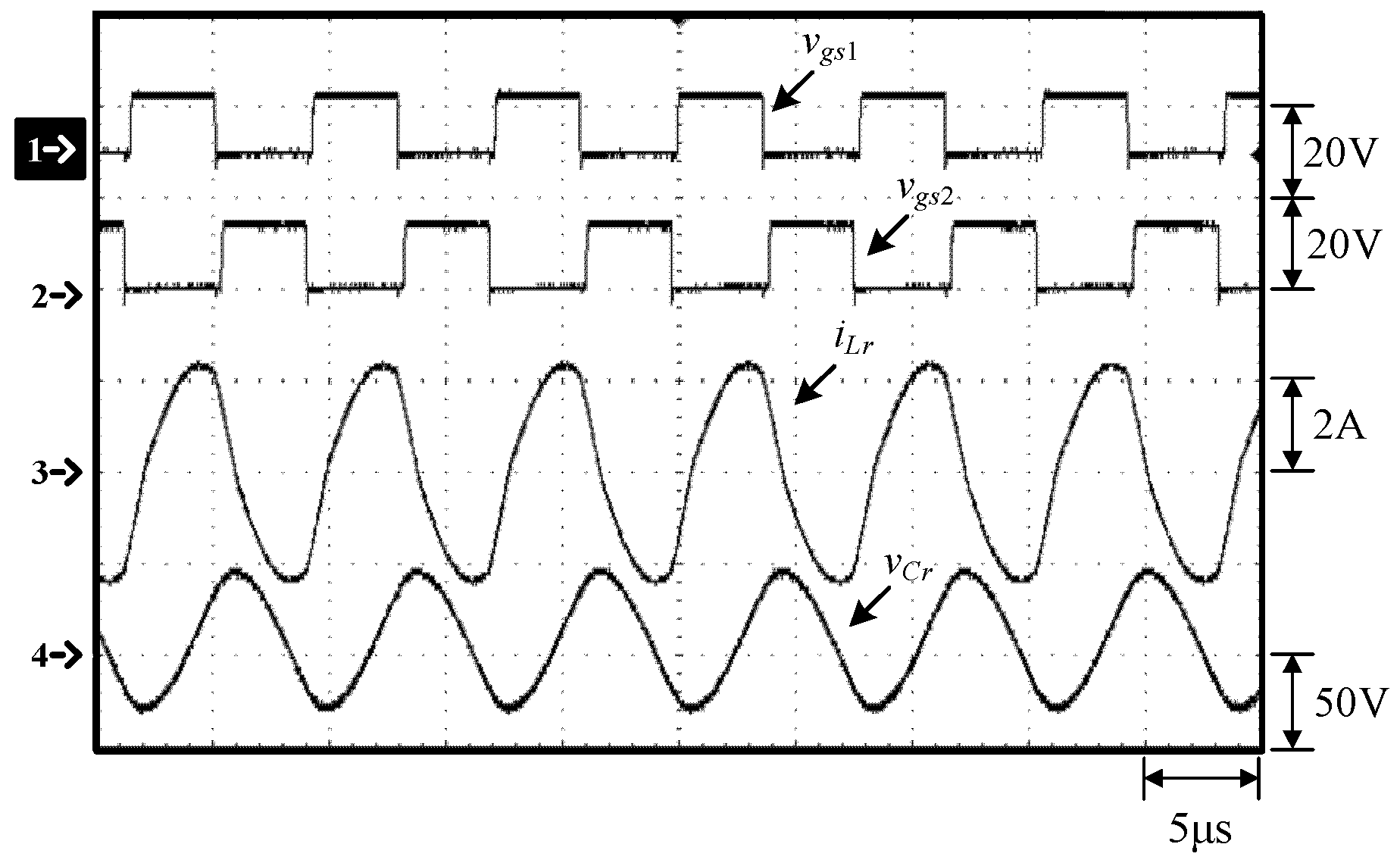
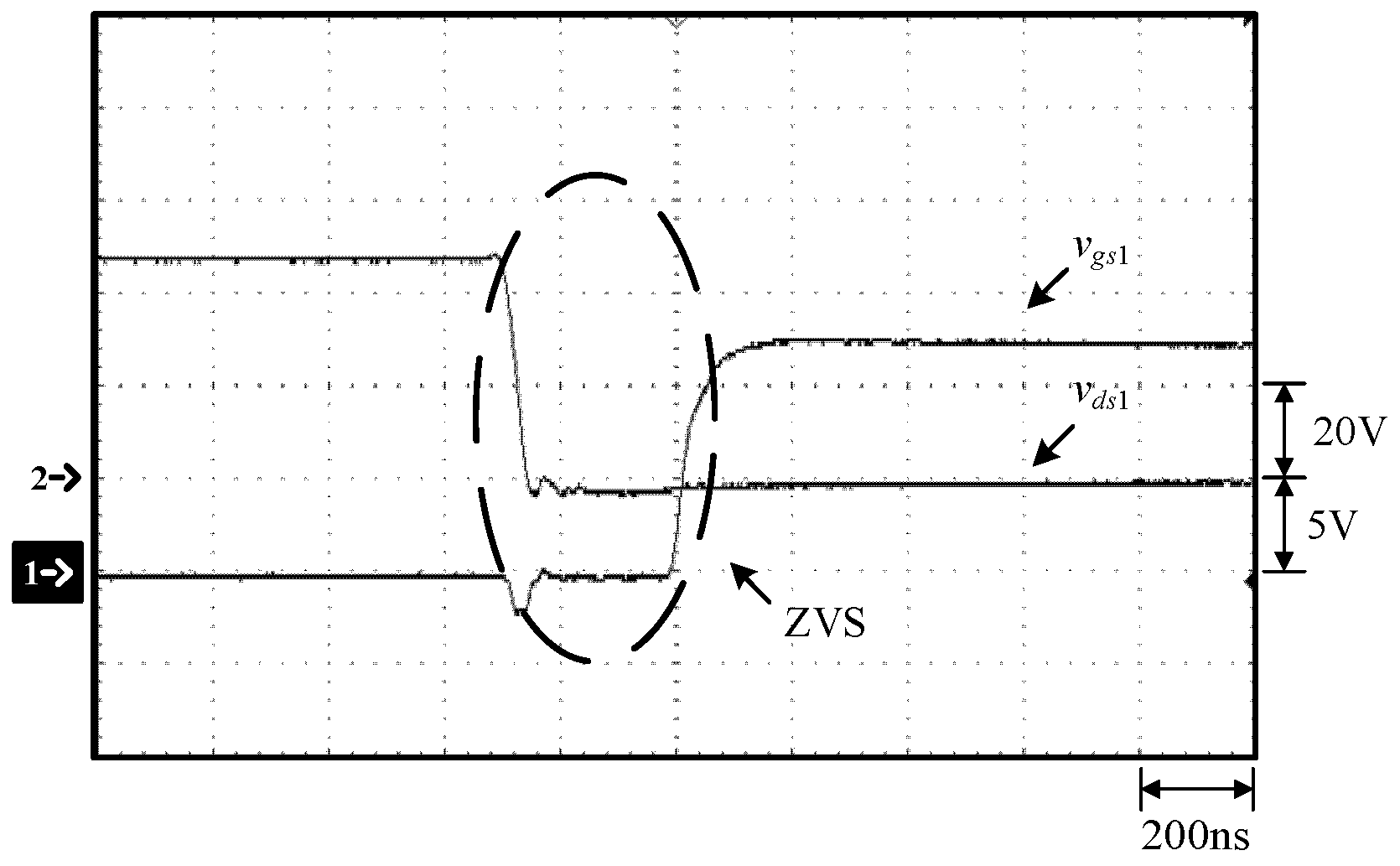
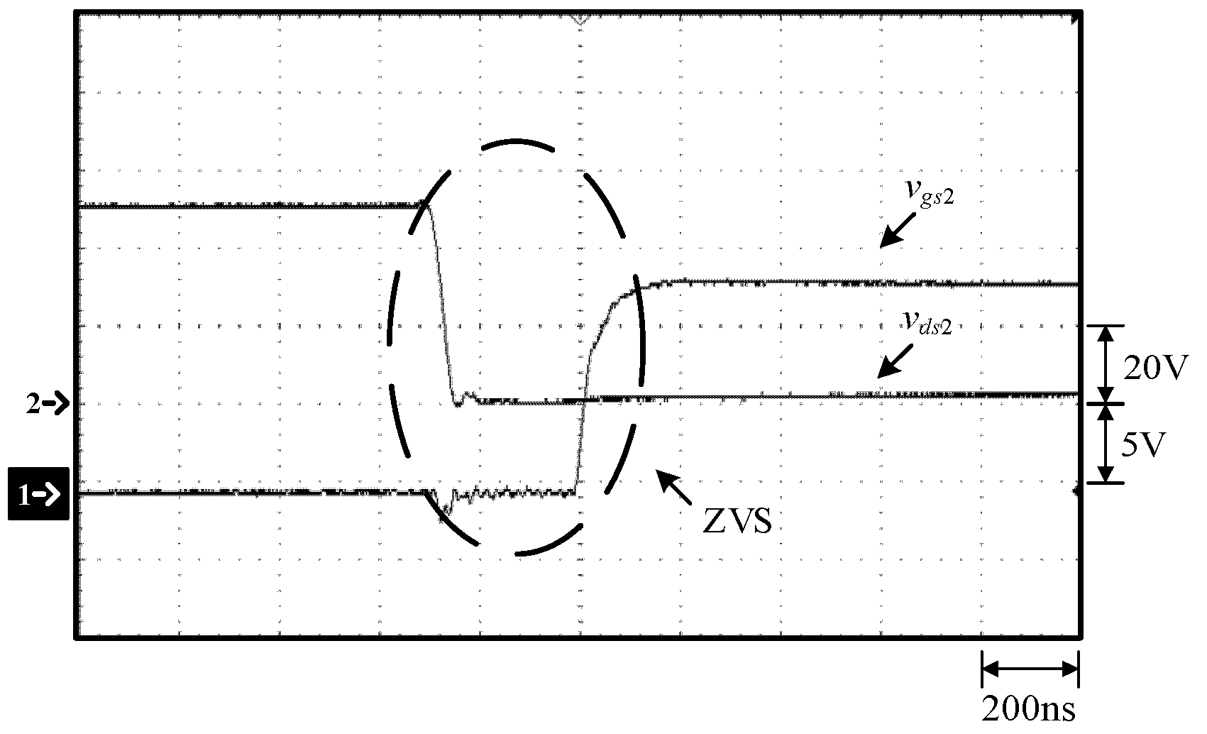
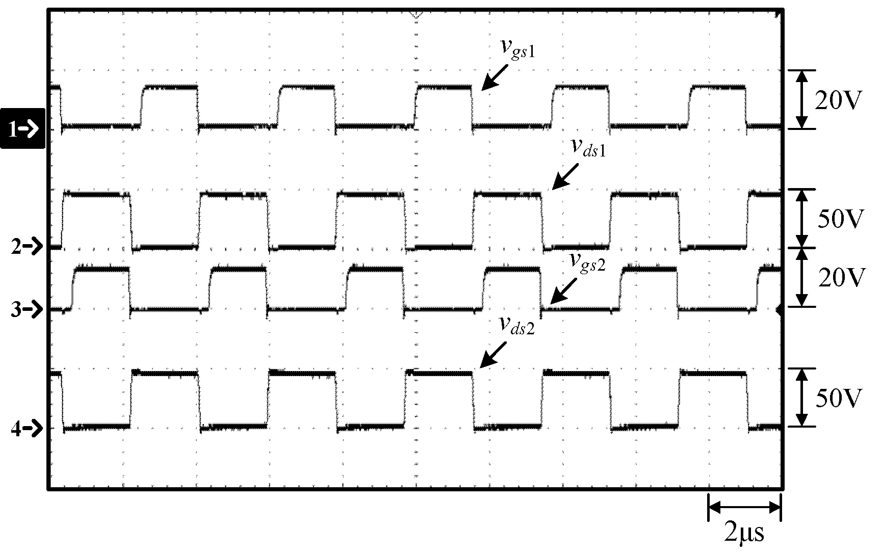
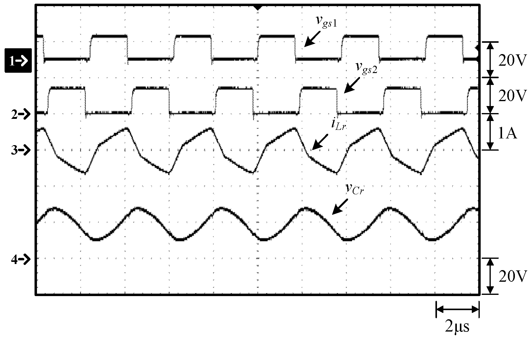
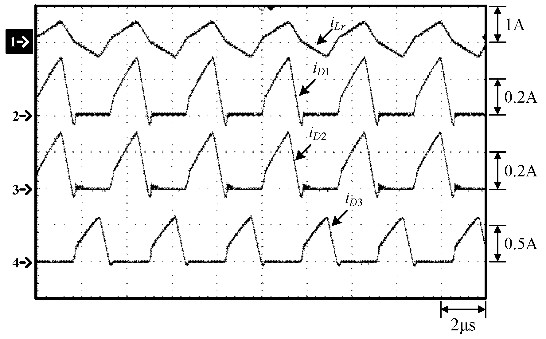
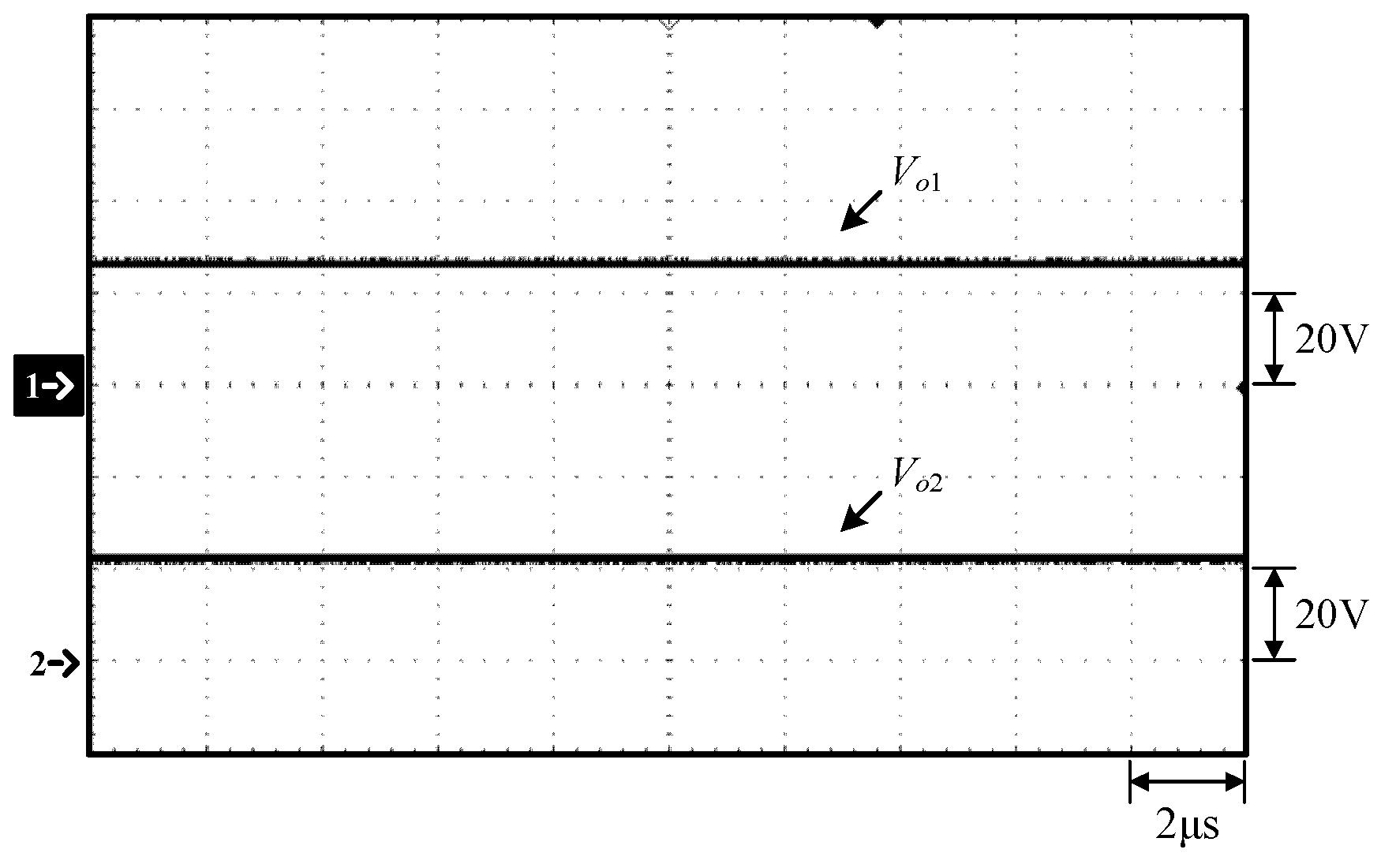
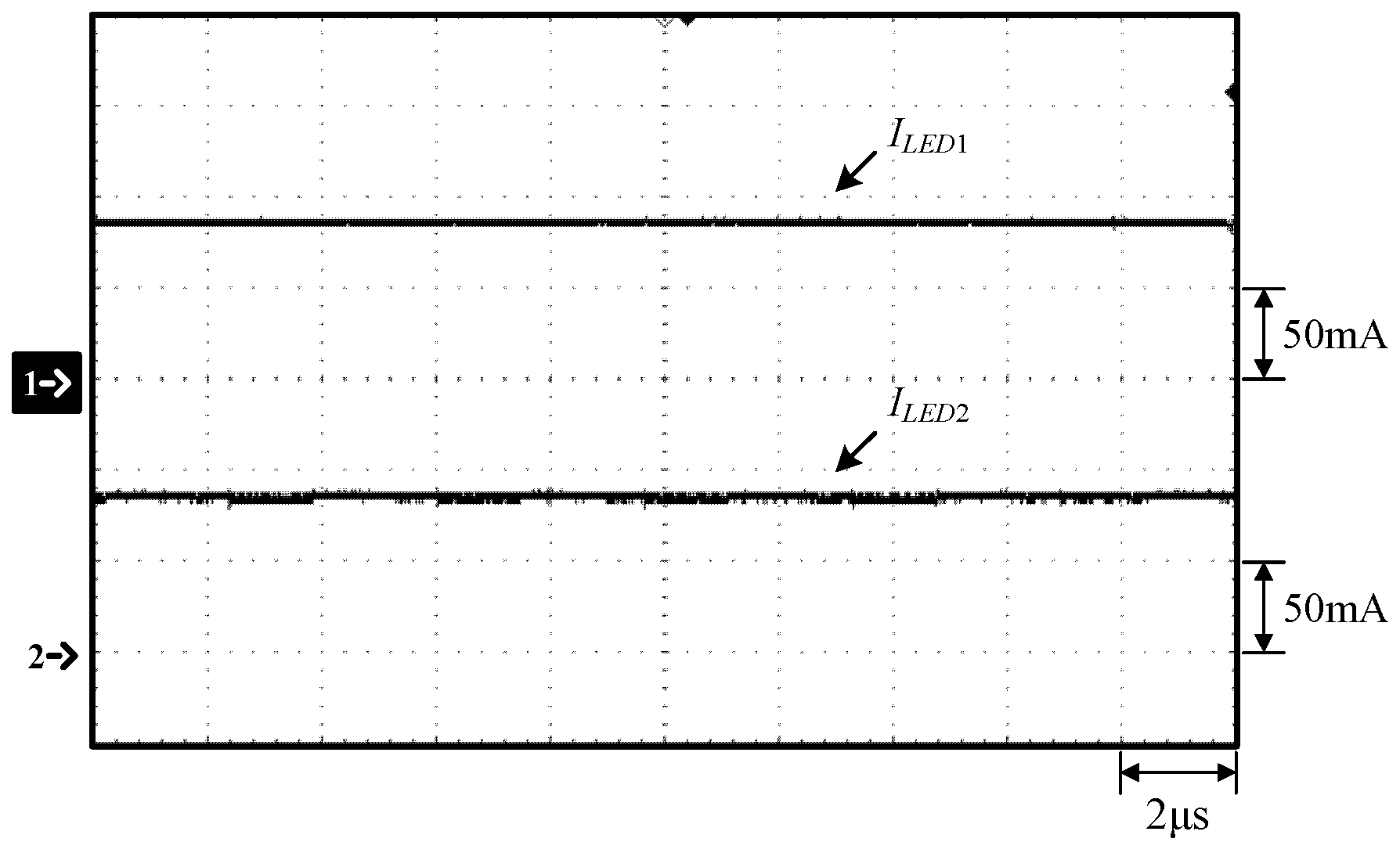
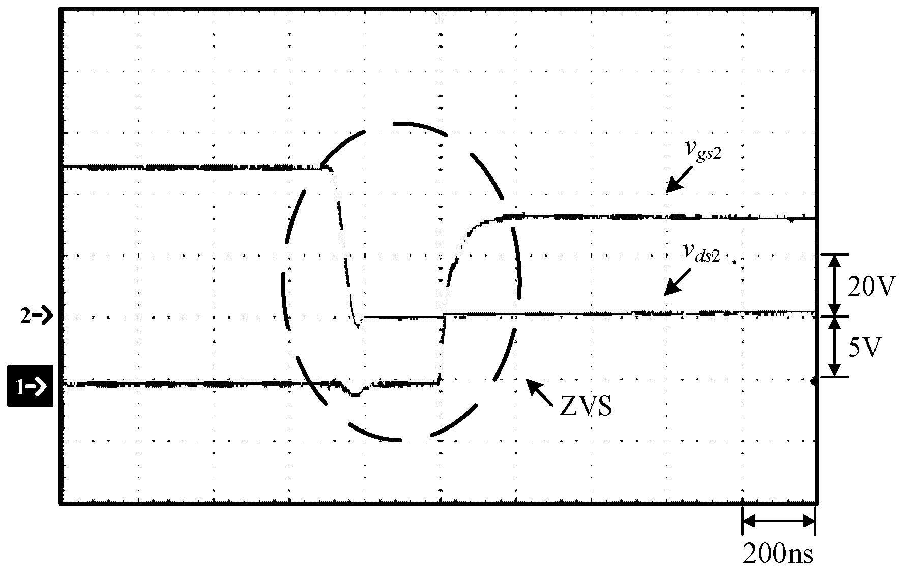
5. Experimental Results

In the following, the waveforms at 100% and 25% loads, the current error percentage, the overall efficiency, and the variable switching frequency are measured.

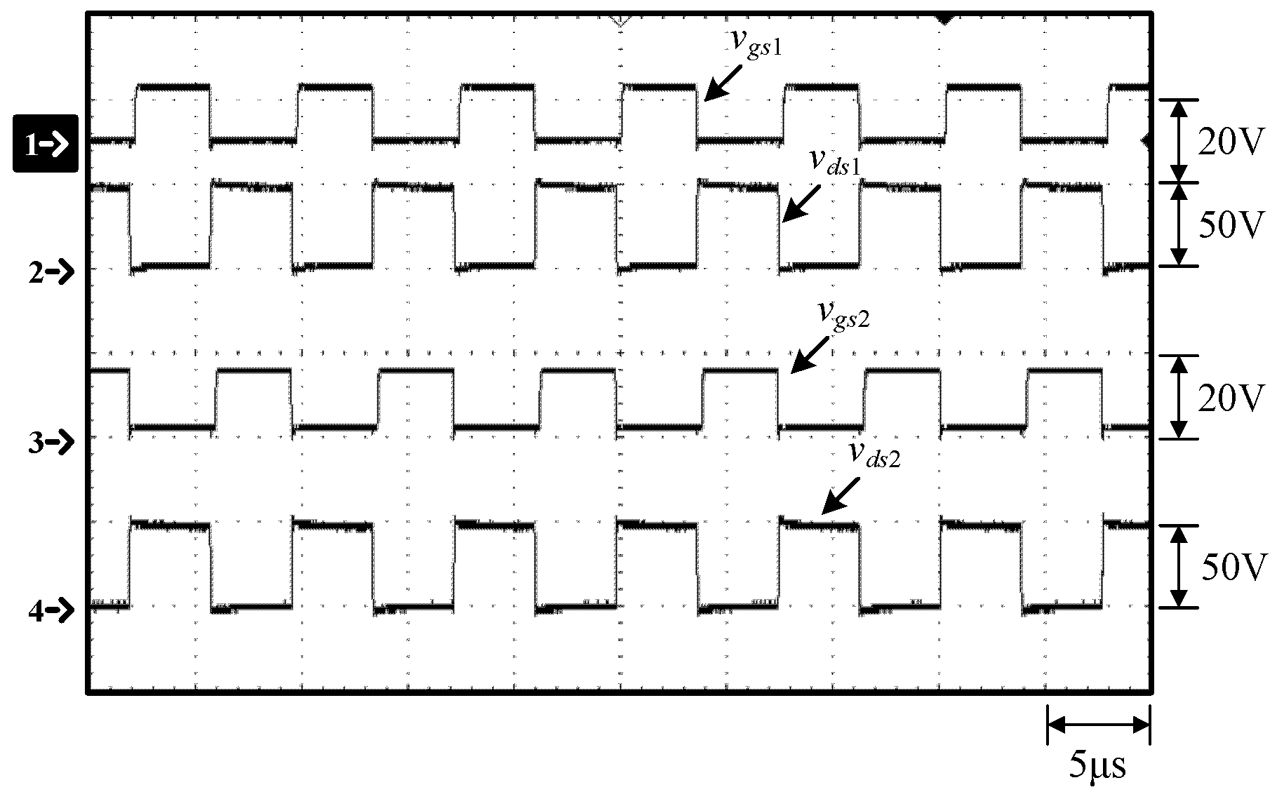
5.1. Waveforms at 100% Load

Figure 9, Figure 10, Figure 11, Figure 12, Figure 13, Figure 14 and Figure 15 show the measured waveforms at 100% load.

5.2. Waveforms at 25% Load

Figure 16, Figure 17, Figure 18, Figure 19, Figure 20, Figure 21 and Figure 22 show the measured waveforms at 25% load.

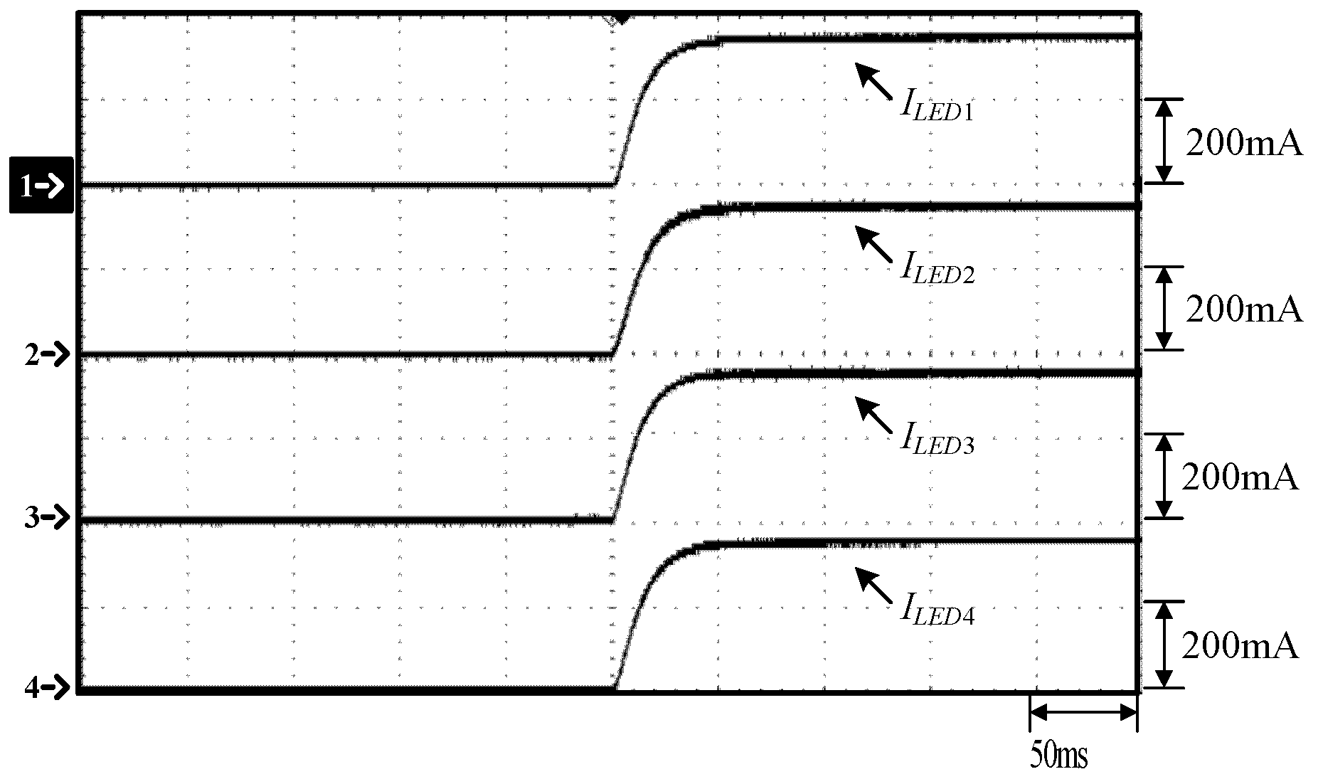
5.3. Waveforms at Startup

Figure 23 shows the LED string currents at startup from zero to 100% load.

5.4. Experimental Comments

From Figure 10, Figure 11, Figure 17 and Figure 18, it can be seen that when the resonant inductor current iLr is in the positive direction, the resonant inductor Lr resonates with the resonant capacitor Cr, and at the same time the resonant inductor current iLr is equally distributed to the diode currents iD1 and iD2 through the differential-mode transformer, while the diode D3 is in the off-state, so the diode current iD3 is zero. When the resonant inductor current iLr enters the negative flow direction, both the diodes D1 and D2 are cut off, so iD1 and iD2 are zero. Since the diode D3 is on, the resonant inductor current iLr continues to flow through the diode D3 and hence no energy is transferred to the output. In addition, as the switching frequency moves away from the resonant frequency, the resonant inductor current iLr gradually becomes more linear, different from the sine wave.
From Figure 12, Figure 13, Figure 19 and Figure 20, it can be seen that for any current load, even if the voltages of the LED strings are different due to different numbers of LEDs, the effect of current equalization can be achieved, and the constant current output can be maintained.
As can be seen in Figure 14 and Figure 21, before the switch S1 is turned on, the voltage vds1 of the switch S1 has dropped to zero and hence the switch S1 is with ZVS turn-on. As can be seen in Figure 15 and Figure 22, before the switch S2 is turned on, the voltage vds2 of the switch S1 has dropped to zero and hence the switch S2 is with ZVS turn-on. From 23, it can be seen that there is no inrush current problem. Figure 24 shows the experimental setup.

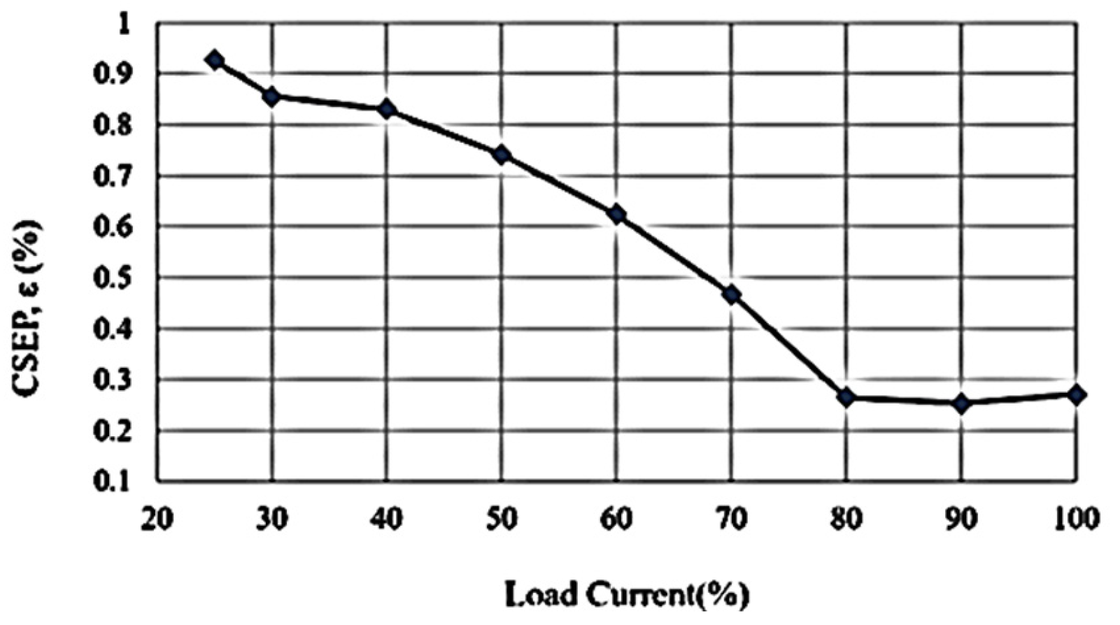
5.5. Current Error Percentage of LED Strings

In this subsection, the measured data of the proposed circuit are used to calculate the current sharing error percentage (CSEP, ε) of the LED strings at different loads:
ε = I L ED y 1 n x = 1 n I L E D x 1 n x = 1 n I L E D x × 100 %
where ε is the current error percentage of LED strings, n is the number of LED strings, ILEDy is the current of the yth LED string, and x = 1 n I L E D x is the sum of currents in all LED strings.
Table 2 and Table 3 show the measurement data of 100% and 25% load, respectively, where the LED string LS1 has 10 LEDs in series and the LED string LS2 has 8 LEDs in series.
From Table 2, the current sharing error percentage ε can be calculated as follows:
ε = 0.3512 1 2 ( 0.3512 + 0.3531 ) 1 2 ( 0.3512 + 0.3534 ) × 100 % = 0.3531 1 2 ( 0.3512 + 0.3531 ) 1 2 ( 0.3512 + 0.3531 ) × 100 % = 0.27 %
From Table 3, the current sharing error percentage ε can be calculated ε as follows:
ε = 0.0855 1 2 ( 0.0855 + 0.0871 ) 1 2 ( 0.0855 + 0.0871 ) × 100 % = 0.0871 1 2 ( 0.0855 + 0.0871 ) 1 2 ( 0.0855 + 0.0871 ) × 100 % = 0.93 %
Figure 25 shows the curve of current sharing error percentage rate from 25% to 100% loads. From this figure, it can be seen that the current error is below 1% across the whole load range. Since the smaller the load is, the larger the current sharing error percentage, the proposed circuit uses 25% load as a design point for designing the differential-mode transformer T1.

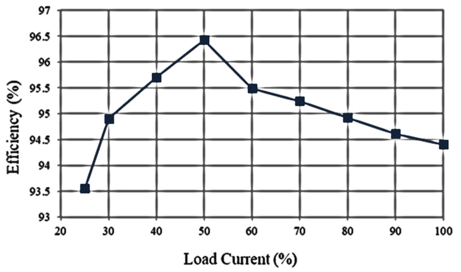
5.6. Efficiency Measurement

First, a digital meter is used to measure the input voltage, input current, and the output voltage and current of each LED string to obtain the input power and output power. Finally, the results are plotted to show the efficiency curve of the actual circuit. Figure 26 displays the efficiency curve efficiency versus load current.
From this figure, it can be seen that the efficiency is about above 93.6% across the whole load range, the maximum efficiency is about 96.4% at 50% load, and the efficiency is about 94.4% at 100% load.

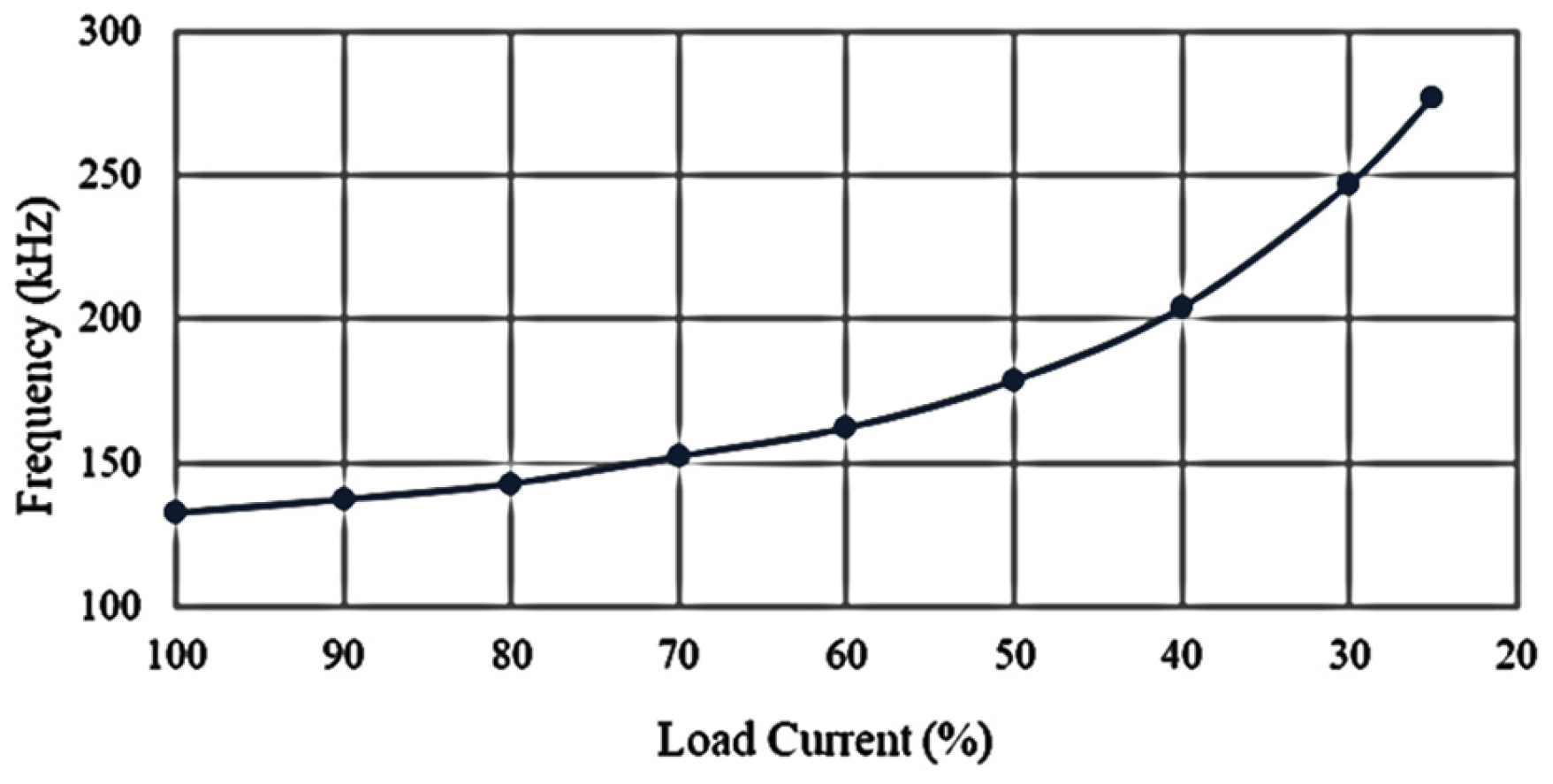
5.7. Switching Frequency Measurement

Figure 27 shows the curve of switching frequency versus load current. The switching frequency is about 132 kHz at 100% load, whereas the switching frequency is 277 kHz at 25% load. Also, from Figure 5, when the load current is higher, the value of Q is larger, so the frequency variation range is smaller; on the contrary, when the load current decreases, the frequency variation range is larger.

6. Literature Comparison

Table 4 compares several items of components used in current equalization between the existing and proposed circuits, containing the following: (1) the number of LED strings; (2) the number of diodes required for four LED strings; (3) the wide adjustable load range; (4) the current equalization method; (5) the number of transformers required for four LED strings; (6) the soft switching; and (7) the extension of the number of LED strings.
Studies [12,13] with differential-mode transformer equalization circuit need to use a larger number of diodes to provide the differential-mode transformer with a demagnetization path, and to ensure that this transformer can be completely demagnetized, the switching duty cycle has an upper limit, resulting in the ability to regulate the load being limited. The H-bridge circuit structure proposed in [21] reduces the number of demagnetizing diodes used in [12,13] and improves the load regulation. Study [14] proposes to achieve the current equalization of LED strings by connecting multiple isolation transformers in series, and the current equalization error is mainly determined by the magnitude of the magnetizing inductance of the isolation transformers, which also affects the load regulation capability of the resonant circuit. Therefore, a buck circuit is added in the front stage of the proposed circuit to change the duty cycle of the buck circuit, and the resonant circuit in the back stage adopts the fixed frequency operation to regulate the load current. In addition, in this current equalization method, it will lead to a relatively poor extension of the number of LED strings.

7. Conclusions

In this study, a non-isolated series resonant ZVS LED driver with current equalization is presented. In this LED driver, a differential-mode transformer is used to balance the LED currents. Furthermore, the series resonant converter uses a controlled frequency modulation to vary the amount of energy transferred to the outputs as well as to realize the turn-on ZVS. In addition, only the current in one LED string needs to be sensed, while the current in the other LED string is automatically determined by the differential-mode transformer, thereby simplifying control. In particular, the relationship between the magnetizing inductance and the current sharing error percentage is derived and can be used to design the value of the magnetizing inductance. Additionally, from the experimental results, the current sharing error percentage is 0.27% at 100% load, and the efficiency is above 93.6% for any loads, with a maximum efficiency of 96.4%. In this research, the limitation is that the proposed circuit has a problem of circulating current, so the higher the load current is, the higher the power loss. This will be solved by adding more LED strings to the circuit.

Author Contributions

Conceptualization, K.-I.H. and J.-Y.L.; methodology, J.-Y.L. and K.-I.H.; PSIM 9.1 software, J.-Y.L.; validation, J.-Y.L. and K.-I.H.; formal analysis, J.-Y.L. and K.-I.H.; investigation, J.-Y.L.; resources, K.-I.H.; data curation, J.-Y.L.; writing—original draft preparation, K.-I.H.; writing—review and editing, K.-I.H.; visualization, J.-Y.L.; supervision, K.-I.H.; project administration, K.-I.H.; funding acquisition, K.-I.H. All authors have read and agreed to the published version of the manuscript.

Funding

This research was funded by the Ministry of Science and Technology, Taiwan, under Grant Number NSTC112-2221-E-027-015-MY2.

Data Availability Statement

Data are contained within this article.

Conflicts of Interest

The authors declare no conflicts of interest.

References

  1. De Almeida, A.; Santos, B.; Paolo, B.; Quicheron, M. Solid state lighting review–Potential and challenges in Europe. Renew. Sustain. Energy Rev. 2014, 34, 30–48. [Google Scholar] [CrossRef]
  2. Ng, S.K.; Loo, K.H.; Lai, Y.M.; Mok, K.T.; Tse, C.K. Variable bi-level phase-shifted driving method for high-power RGB LED lamps. In Proceedings of the IEEE International Conference on Power Electronics—ECCE Asia, Jeju, Republic of Korea, 30 May–3 June 2011; pp. 782–787. [Google Scholar]
  3. Burgyan, L.; Prinz, F. High Efficiency LED Driver. U.S. Patent 6690146B2, 10 February 2004. [Google Scholar]
  4. Hu, Y.; Jiang, L.; Wen, W.; Yan, W.; Ding, R. A new adaptive drive voltage approach for LED Driver. In Proceedings of the IEEE Applied Power Electronics Conference and Exposition (APEC), Anaheim, CA, USA, 17–21 March 2019; pp. 721–726. [Google Scholar]
  5. Qu, X.; Wong, S.-C.; Tse, C.K. Noncascading structure for electronic ballast design for multiple LED lamps with independent brightness control. IEEE Trans. Power Electron. 2010, 25, 331–340. [Google Scholar]
  6. Hu, Q.; Zane, R. LED driver circuit with series-input-connected converter cells operating in continuous conduction mode. IEEE Trans. Power Electron. 2010, 25, 574–582. [Google Scholar]
  7. Kim, H.-C.; Yoon, C.S.; Jeong, D.-K.; Kim, J. A single-inductor, multiple-channel current-balancing LED driver for display backlight applications. IEEE Trans. Ind. Appl. 2014, 50, 4077–4081. [Google Scholar] [CrossRef]
  8. Qu, X.; Wong, S.-C.; Tse, C.K. A current balancing scheme with high luminous efficiency for high power LED lighting. In Proceedings of the IECON 2013—39th Annual Conference of the IEEE Industrial Electronics Society, Vienna, Austria, 10–13 November 2013; pp. 169–174. [Google Scholar]
  9. Liu, P.-J.; Hsu, Y.-C.; Hsu, S.-R. Drain-voltage balance and phase-shifted PWM control schemes for high-efficiency parallel-string dimmable LED drivers. IEEE Trans. Ind. Electron. 2018, 65, 6168–6176. [Google Scholar] [CrossRef]
  10. Wang, J.; Zhang, J.; Huang, X.; Xu, L. A family of capacitive current balancing methods for multi-output LED drivers. In Proceedings of the 2011 Twenty-Sixth Annual IEEE Applied Power Electronics Conference and Exposition (APEC), Fort Worth, TX, USA, 6–11 March 2011; pp. 2040–2046. [Google Scholar]
  11. Do, D.-T.; Cha, H.; Nguyen, B.L.-H.; Kim, H.-G. Two-channel interleaved buck LED driver using current-balancing capacitor. IEEE J. Emerg. Sel. Top. Power Electron. 2018, 6, 1306–1313. [Google Scholar] [CrossRef]
  12. Hwu, K.I.; Chou, S.-C. A simple current-balancing converter for LED lighting. In Proceedings of the 2009 Twenty-Fourth Annual IEEE Applied Power Electronics Conference and Exposition, Washington, DC, USA, 15–19 February 2009; pp. 587–590. [Google Scholar]
  13. Hwu, K.I.; Tu, W.C.; Hong, M.J. A dimmable LED driver based on current balancing transformer with magnetizing energy recycling considered. J. Disp. Technol. 2014, 10, 388–395. [Google Scholar] [CrossRef]
  14. Chen, X.; Huang, D.; Li, Q.; Lee, F.C. Multichannel LED driver with LCC resonant converter. IEEE J. Emerg. Sel. Top. Power Electron. 2015, 3, 589–598. [Google Scholar] [CrossRef]
  15. Zhang, X.; Cai, H.; Guan, Y.; Han, S.; Wang, Y.; Dalla, C.; Marco, A.; Alonso, J.M.; Xu, D. A soft-switching transformer-less step-down converter based on resonant current balance module. IEEE Trans. Power Electron. 2021, 7, 8206–8218. [Google Scholar] [CrossRef]
  16. Zhang, X.; Cai, H.; Sun, L.; Liu, H.; Wang, Y.; Xu, D. A two-channel LED driver with automatic current balance and soft-switching. In Proceedings of the 2020 IEEE 9th International Power Electronics and Motion Control Conference (IPEMC2020-ECCE Asia), Nanjing, China, 29 November–2 December 2020; pp. 2594–2598. [Google Scholar]
  17. Jiang, W.-Z.; Hwu, K.-I.; Yau, Y.-T.; Chen, H.-H. Two-channel LLC resonant LED driver based on current sharing capacitor. In Proceedings of the 2021 IEEE International Future Energy Electronics Conference (IEFFC), Taipei, Taiwan, 16–19 November 2021; pp. 1–7. [Google Scholar]
  18. Molavi, N.; Farzanehfard, H. A nonisolated wide-range resonant converter for LED driver applications. IEEE Trans. Ind. Electron. 2023, 70, 8939–8946. [Google Scholar] [CrossRef]
  19. Hsieh, Y.-C.; Cheng, H.-L.; Chang, E.-C.; Huang, W.-D. A soft-switching interleaved buck–boost LED driver with coupled inductor. IEEE Trans. Power Electron. 2022, 37, 577–587. [Google Scholar] [CrossRef]
  20. Lee, S.-W.; Choe, H.-J.; Yun, J.-J. Performance improvement of a boost LED driver with high voltage gain for edge-lit LED backlights. IEEE Trans. Circuits Syst. II Express Briefs 2018, 65, 481–485. [Google Scholar] [CrossRef]
  21. Jiang, W.-Z.; Hwu, K.-I. A dimmable LED driver based on H-bridge and differential-mode transformer. In Proceedings of the 2018 7th International Symposium on Next Generation Electronics (ISNE), Taipei, Taiwan, 7–9 May 2018; pp. 1–3. [Google Scholar]
Figure 1. System configuration: (a) overall system; (b) DSP algorithm.
Energies 18 03071 g001
Figure 2. Key waveforms relevant to the proposed circuit.
Energies 18 03071 g002
Figure 3. Current flow: (a) state 1; (b) state 2; (c) state 3; (d) state 4; (e) state 5; (f) state 6; (g) state 7; (h) state 8; (i) state 9.
Energies 18 03071 g003aEnergies 18 03071 g003bEnergies 18 03071 g003c
Figure 4. s-domain equivalent of the proposed circuit.
Energies 18 03071 g004
Figure 5. Voltage gain curve of the proposed circuit.
Energies 18 03071 g005
Figure 6. Current equalization circuit based on the differential-mode transformer.
Energies 18 03071 g006
Figure 7. Operating behavior of magnetizing inductance.
Energies 18 03071 g007
Figure 8. Four-channel LED circuit.
Energies 18 03071 g008
Figure 9. Waveforms at 100% load: (1) vgs1; (2) vds1; (3) vgs2; (4) vds2.
Energies 18 03071 g009
Figure 10. Waveforms at 100% load: (1) vgs1; (2) vgs2; (3) iLr; (4) vCr.
Energies 18 03071 g010
Figure 11. Waveforms at 100% load: (1) iLr; (2) iD1; (3) iD2; (4) iD3.
Energies 18 03071 g011
Figure 12. Waveforms at 100% load: (1) Vo1; (2) Vo2.
Energies 18 03071 g012
Figure 13. Waveforms at 100% load: (1) ILED1; (2) ILED2.
Energies 18 03071 g013
Figure 14. Waveforms at 100% load: (1) vgs1; (2) vds1.
Energies 18 03071 g014
Figure 15. Waveforms at 100% load: (1) vgs2; (2) vds2.
Energies 18 03071 g015
Figure 16. Waveforms at 25% load: (1) vgs1; (2) vds1; (3) vgs2; (4) vds2.
Energies 18 03071 g016
Figure 17. Waveforms at 25% load: (1) vgs1; (2) vgs2; (3) iLr; (4) vCr.
Energies 18 03071 g017
Figure 18. Waveforms at 25% load: (1) iLr; (2) iD1; (3) iD2; (4) iD3.
Energies 18 03071 g018
Figure 19. Waveforms at 25% load: (1) Vo1; (2) Vo2.
Energies 18 03071 g019
Figure 20. Waveforms at 25% load: (1) ILED1; (2) ILED2.
Energies 18 03071 g020
Figure 21. Waveforms at 25% load: (1) vgs1; (2) vds1.
Energies 18 03071 g021
Figure 22. Waveforms at 25% load: (1) vgs2; (2) vds2.
Energies 18 03071 g022
Figure 23. LED string currents at startup: (1) ILED1; (2) ILED2; (3) ILED3; (4) ILED4.
Energies 18 03071 g023
Figure 24. Experimental setup: (a) top layer; (b) bottom layer.
Energies 18 03071 g024
Figure 25. Current sharing error percentage ε from 25% to 100% loads.
Energies 18 03071 g025
Figure 26. Curve of efficiency versus load current.
Energies 18 03071 g026
Figure 27. Curve of switching frequency versus load current.
Energies 18 03071 g027
Table 1. System specifications.
Rated Input Voltage (Vin)48 V
Rated Output Voltage (Vo,rated)32 V (10 units in a string)
Rated Output Current (Io,rated)0.7 A
Rated Output Power (Po,rated)22.4 W (10 LEDs,10 LEDs)
Unbalanced Output Power (Po,unbalanced)20.16 W (10 LEDs, 8 LEDs)
Resonant Frequency (fr)100 kHz
Quality Factor (Q)2
Absolute   Current   Error   Percentage   ( ε )<1%
Table 2. Measurement data at 100% load.
LS1LS2
ILED (mA)351.2353.1
VLED (V)31.6825.3
Table 3. Measurement data at 25% load.
LS1LS2
ILED (mA)85.5087.10
VLED (V)28.0622.48
Table 4. Comparison between the existing and proposed circuits.
[12][13][21][14]Proposed
Circuit
Number of
LED strings
44444
Number of diodes for four
LED strings
88244
Wide adjustable load rangeNoNoYesYesYes
Current equalization methodTransformerTransformerTransformerTransformer and CapacitorTransformer
Number of transformers for four
LED strings
33323
Soft switchingNoNoNoZVSZVS
Extension of the number of
LED strings
YesYesYesNoYes
Disclaimer/Publisher’s Note: The statements, opinions and data contained in all publications are solely those of the individual author(s) and contributor(s) and not of MDPI and/or the editor(s). MDPI and/or the editor(s) disclaim responsibility for any injury to people or property resulting from any ideas, methods, instructions or products referred to in the content.

