
GaN Power Transistors in Converter Design Techniques


Abstract
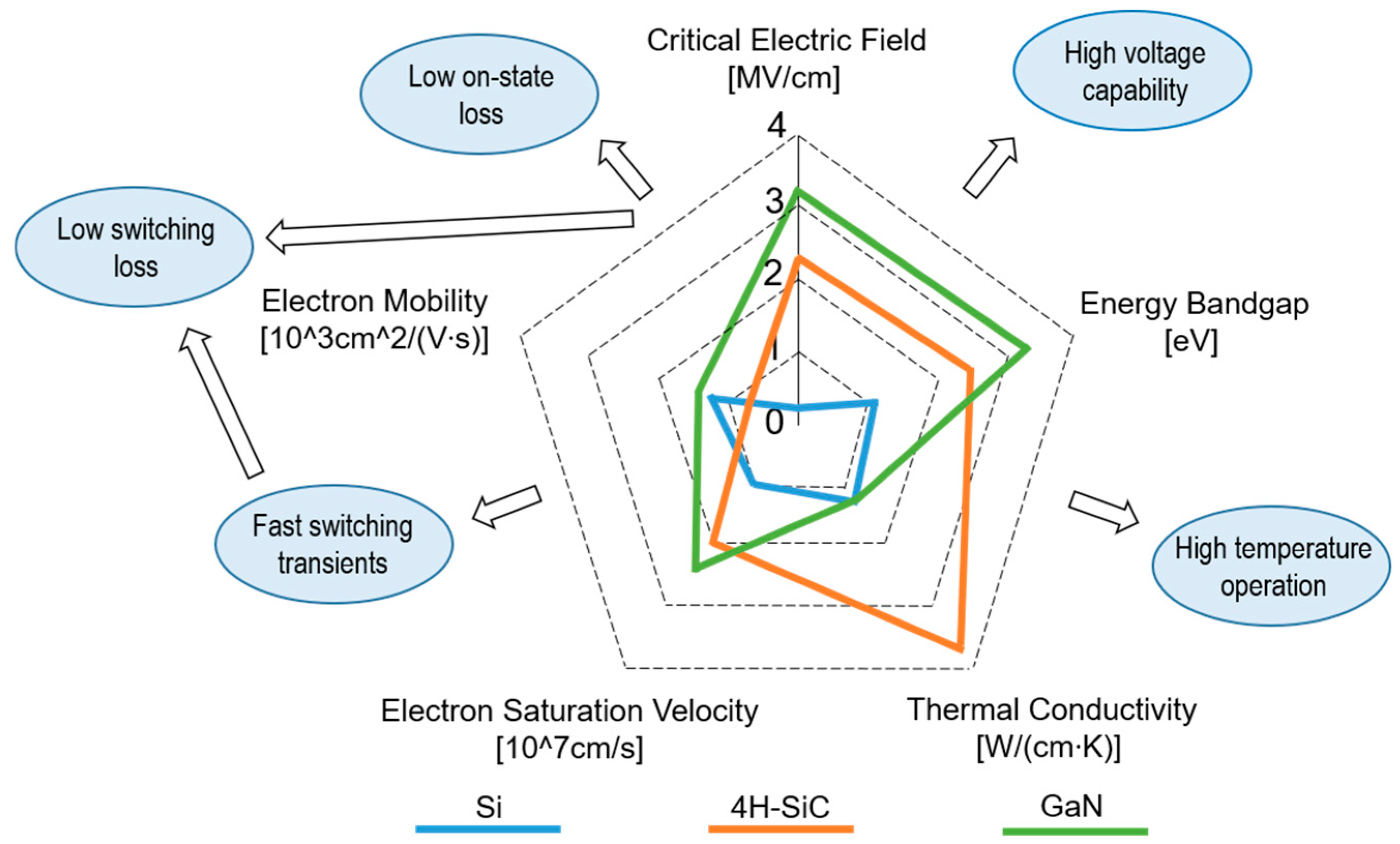
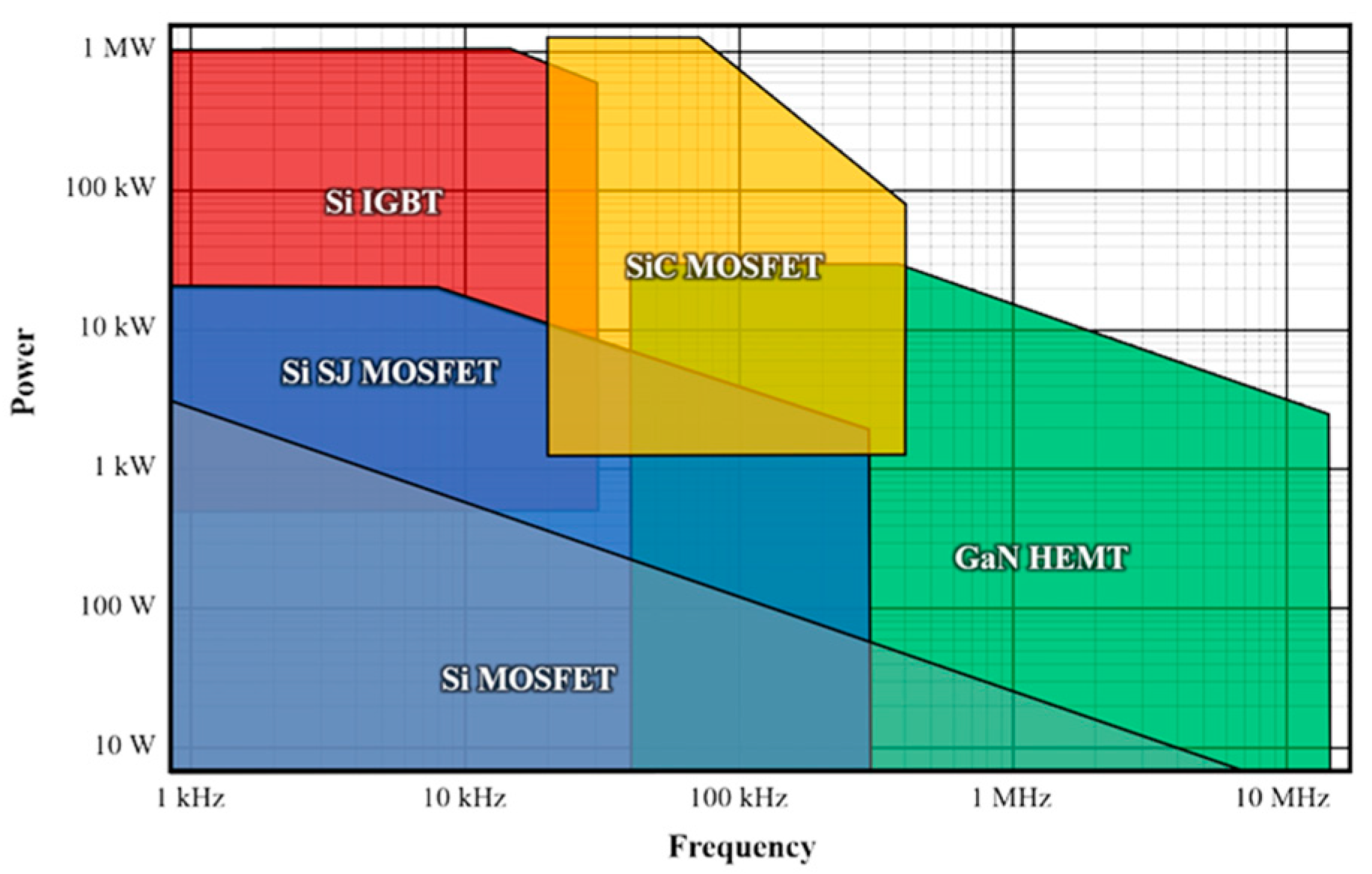
1. Introduction
2. Classification of GaN Power Devices
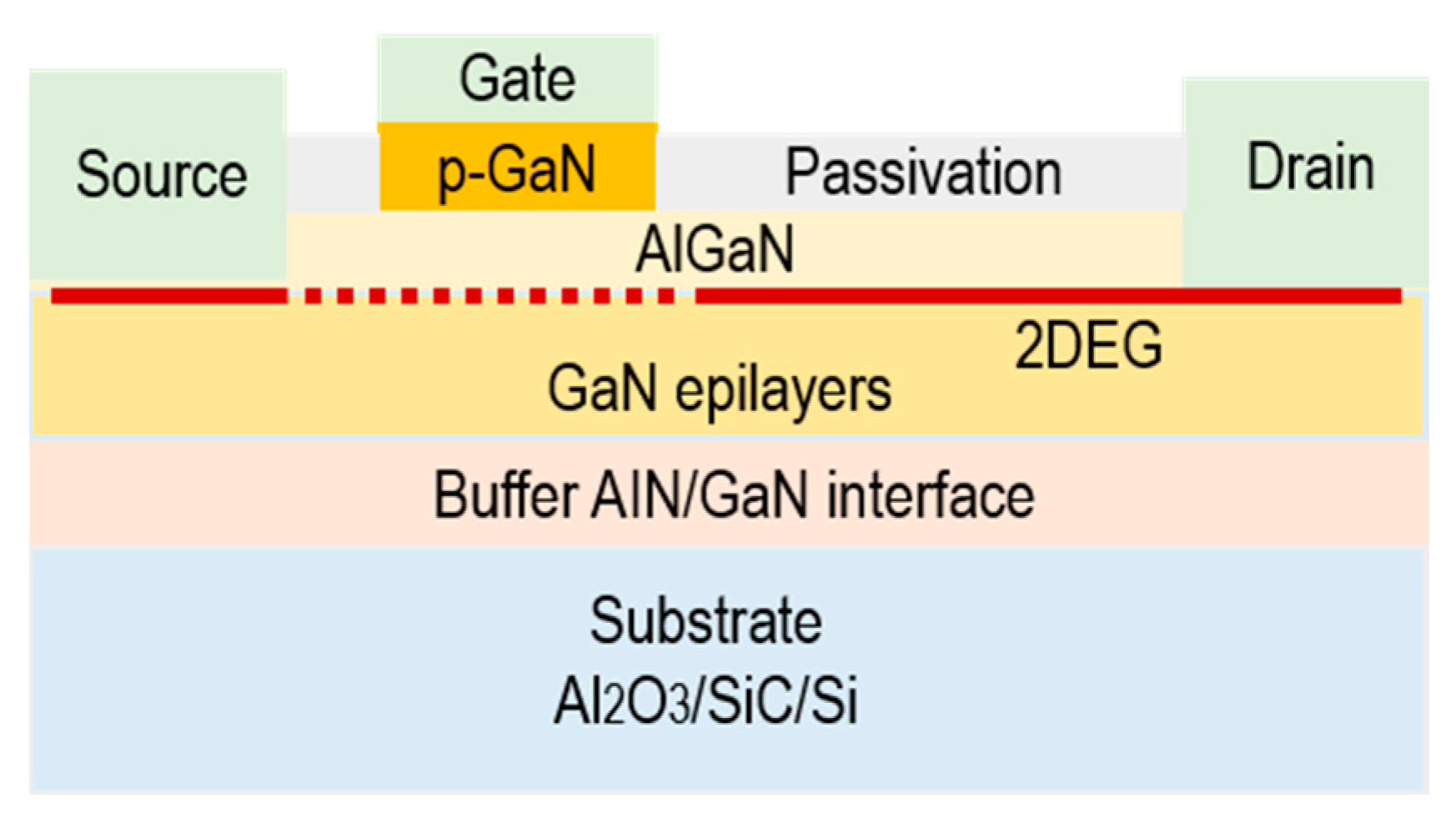
2.1. E-Mode GaN HEMTs
- Ultra-fast switching;
- Zero reverse-recovery charge QRR;
- Low gate charge QG and output charge QOSS;
- Reverse conduction capability;
- Strong on-resistance temperature dependence.
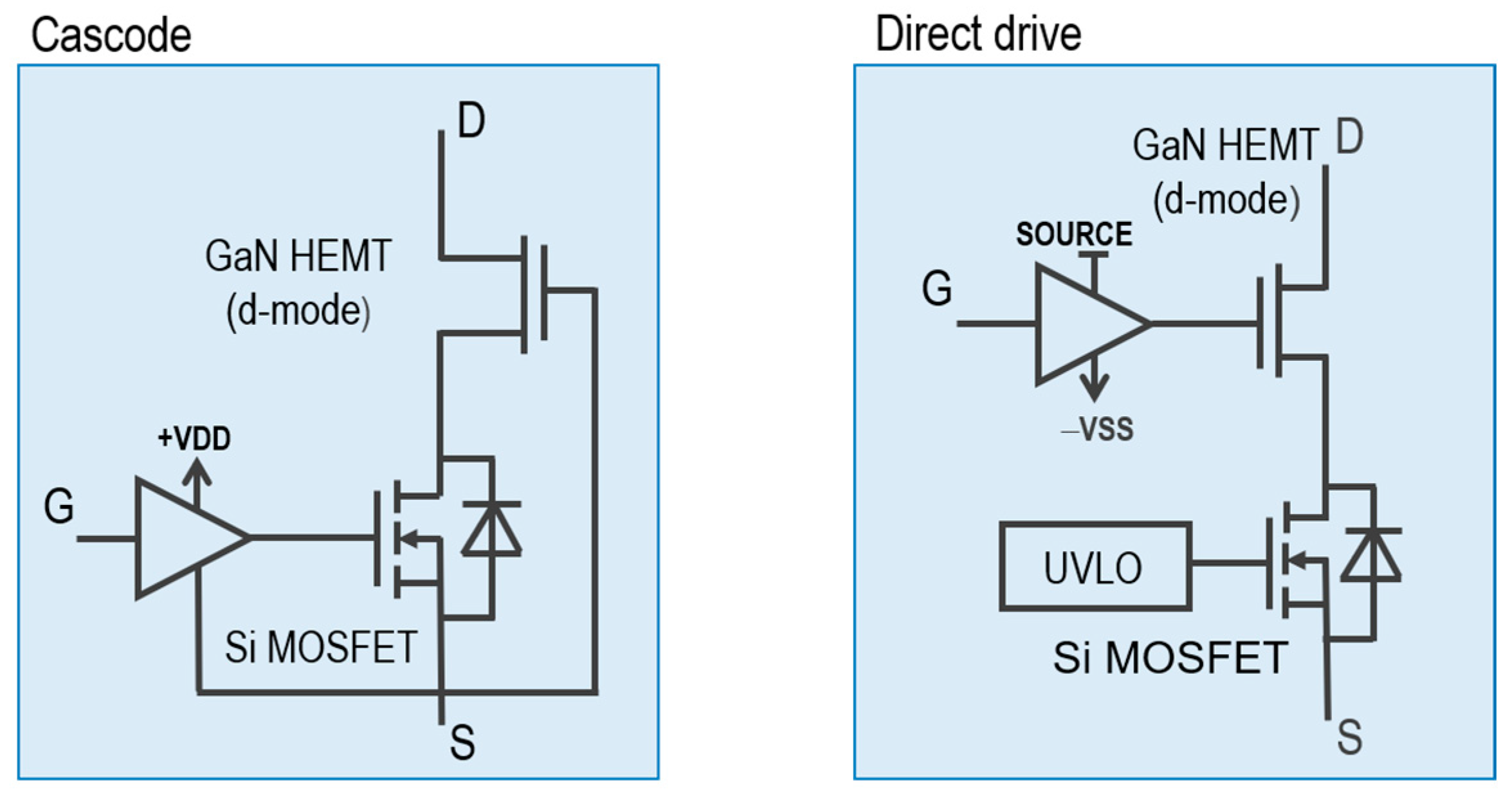
2.2. Hybrid Transistors
- VGS(th) set by the Si MOSFET independent of the d-mode GaN HEMT;
- Standard-level MOSFET drivers can be used;
- High immunity to drain voltage gradients dv/dt;
- Enhanced inrush current capability;
- Low gate charge QG and output charge QOSS;
- Reverse conduction capability;
- Very low reverse-recovery charge QRR.
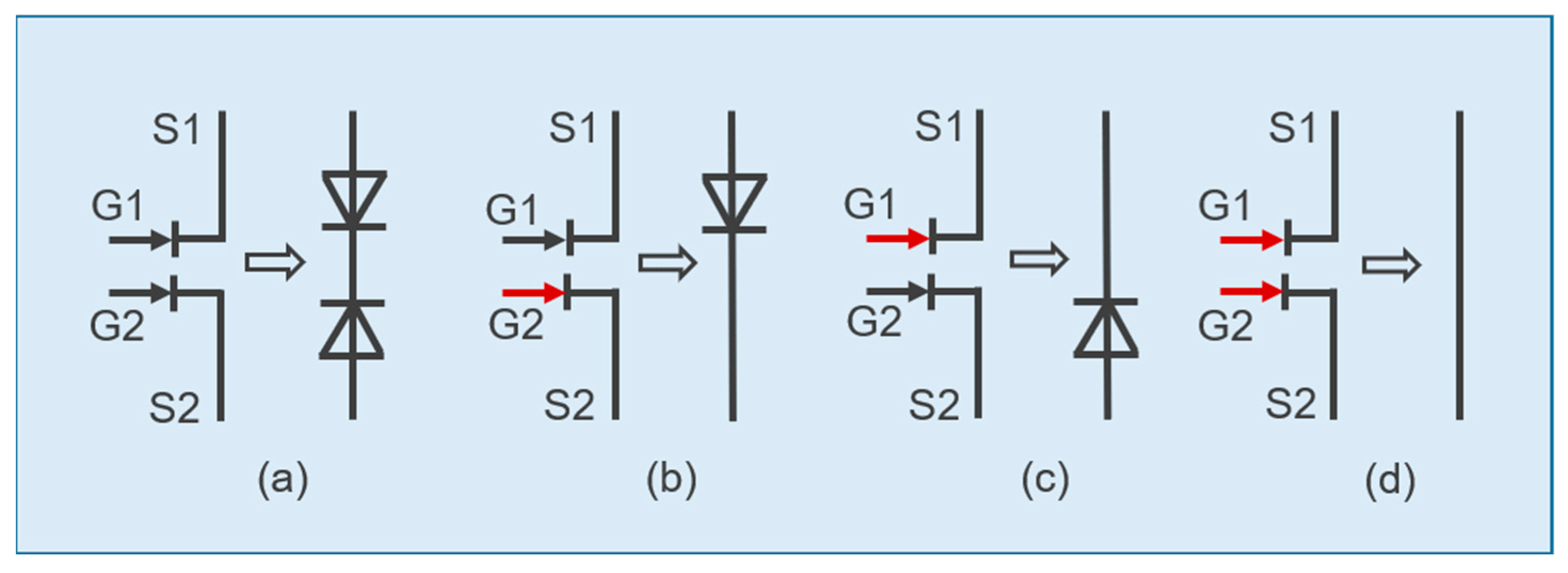
2.3. Bidirectional GaN Transistors
2.4. Vertical GaN Transistors
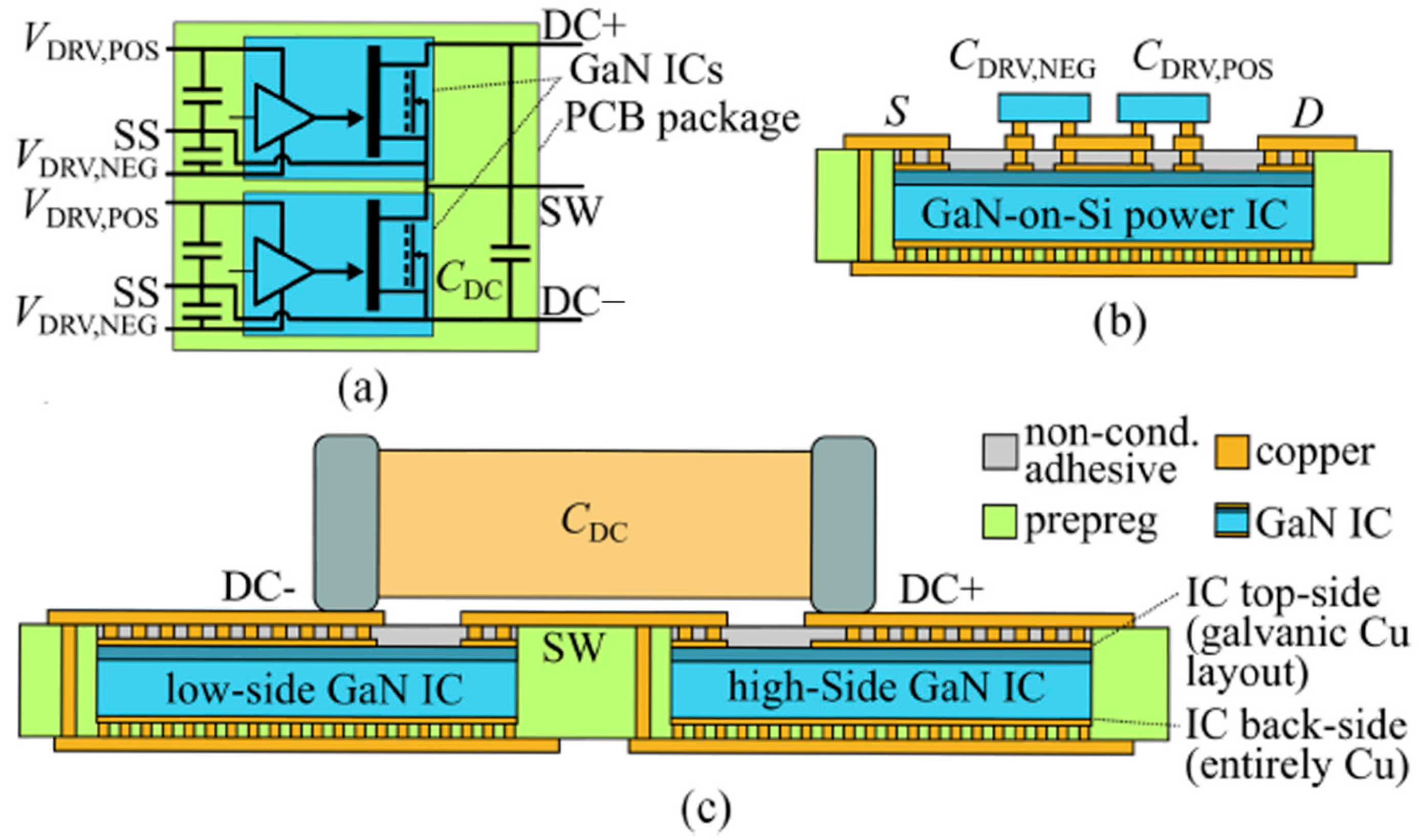
3. GaN Integration Techniques
4. Half-Bridge Implementation Case Study
4.1. Power Loop and Gate Loop Inductances
4.2. The Impact of Stray Capacitance
4.3. Planar 2D Layout of PCB
4.4. 2.5D Power Chip-on-Chip Layout of PCB
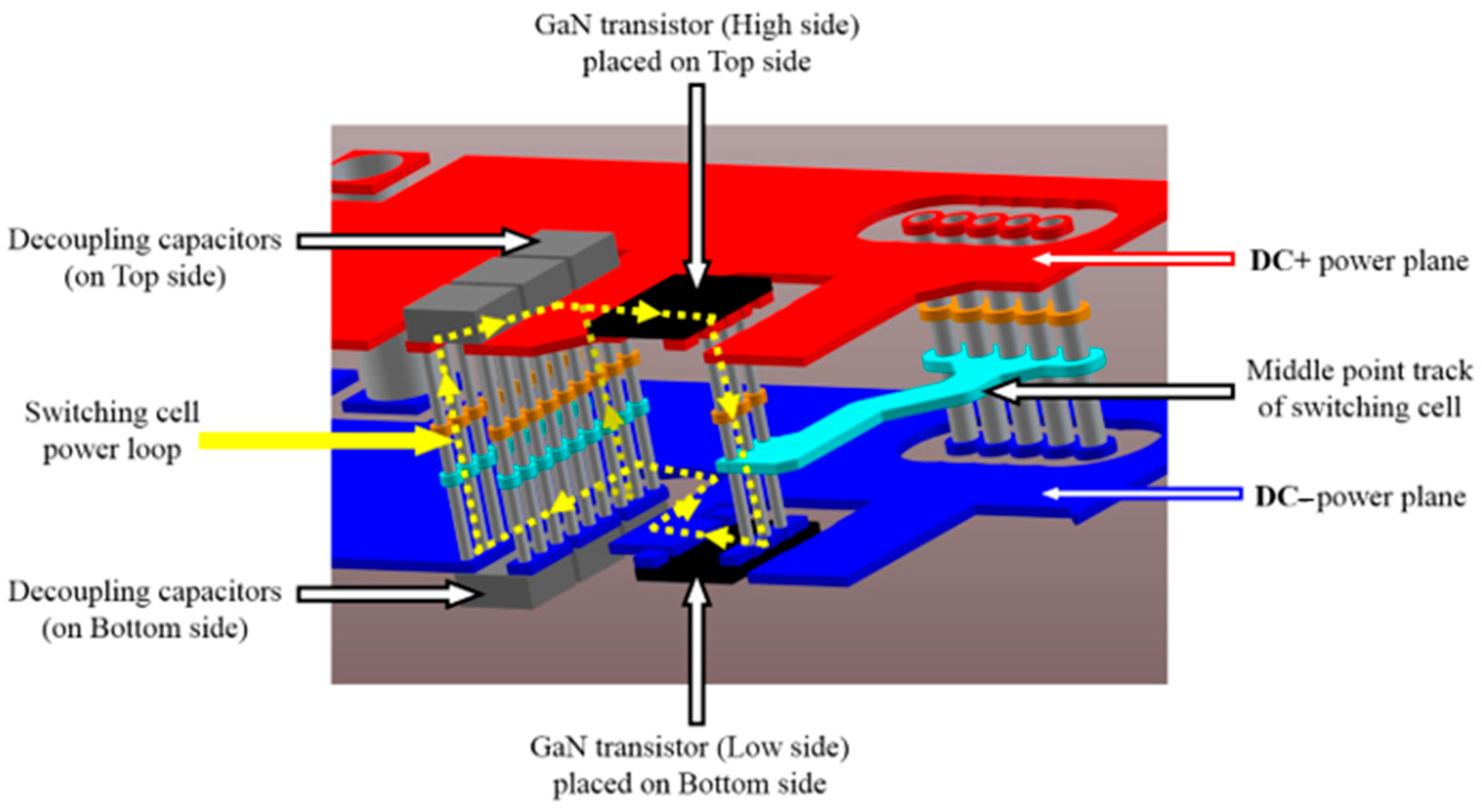
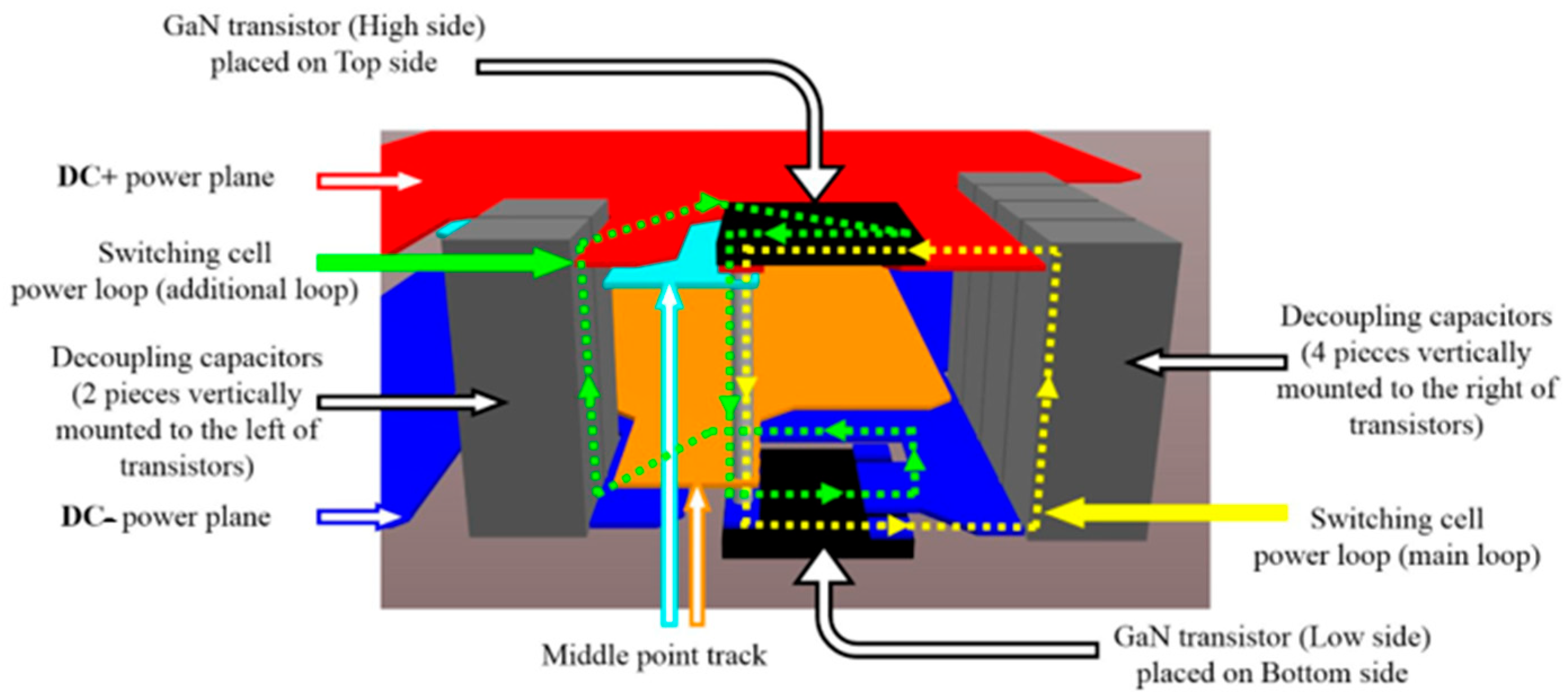
4.5. 3D Power Chip-on-Chip Layout of PCB
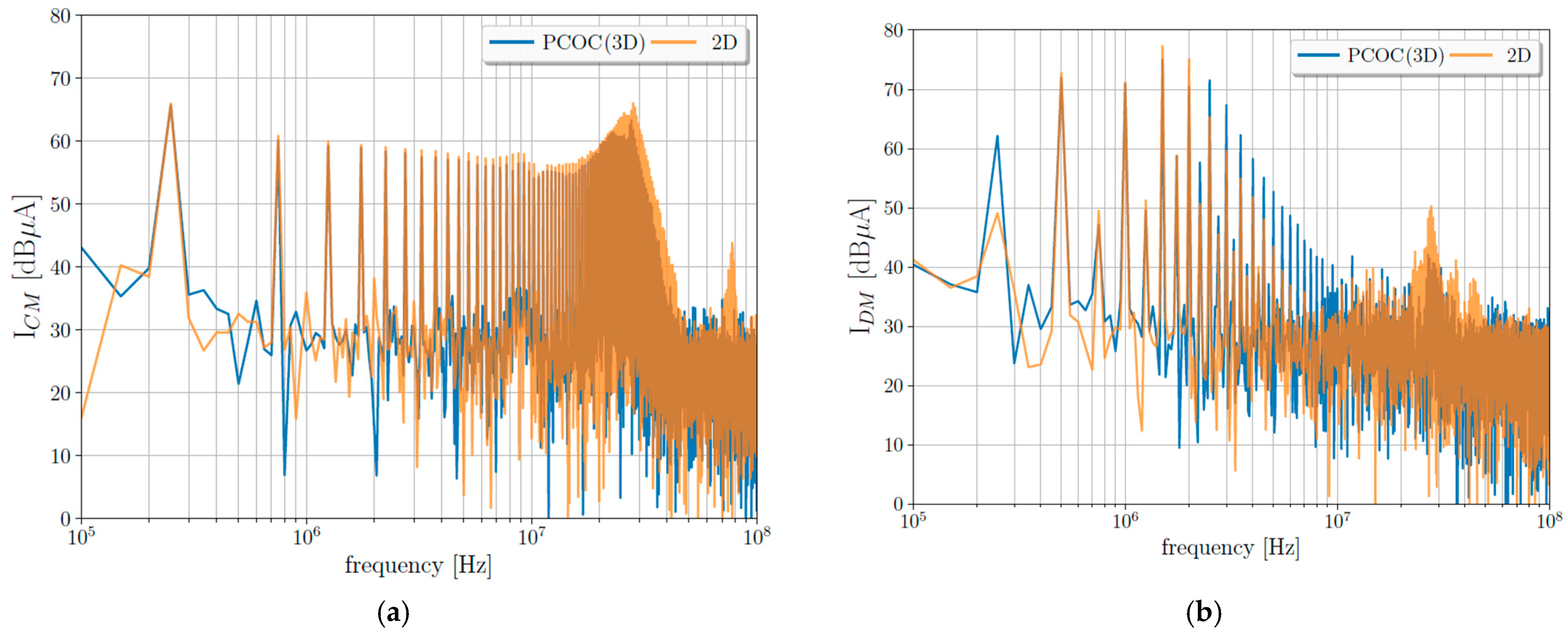
4.6. Simulation Results
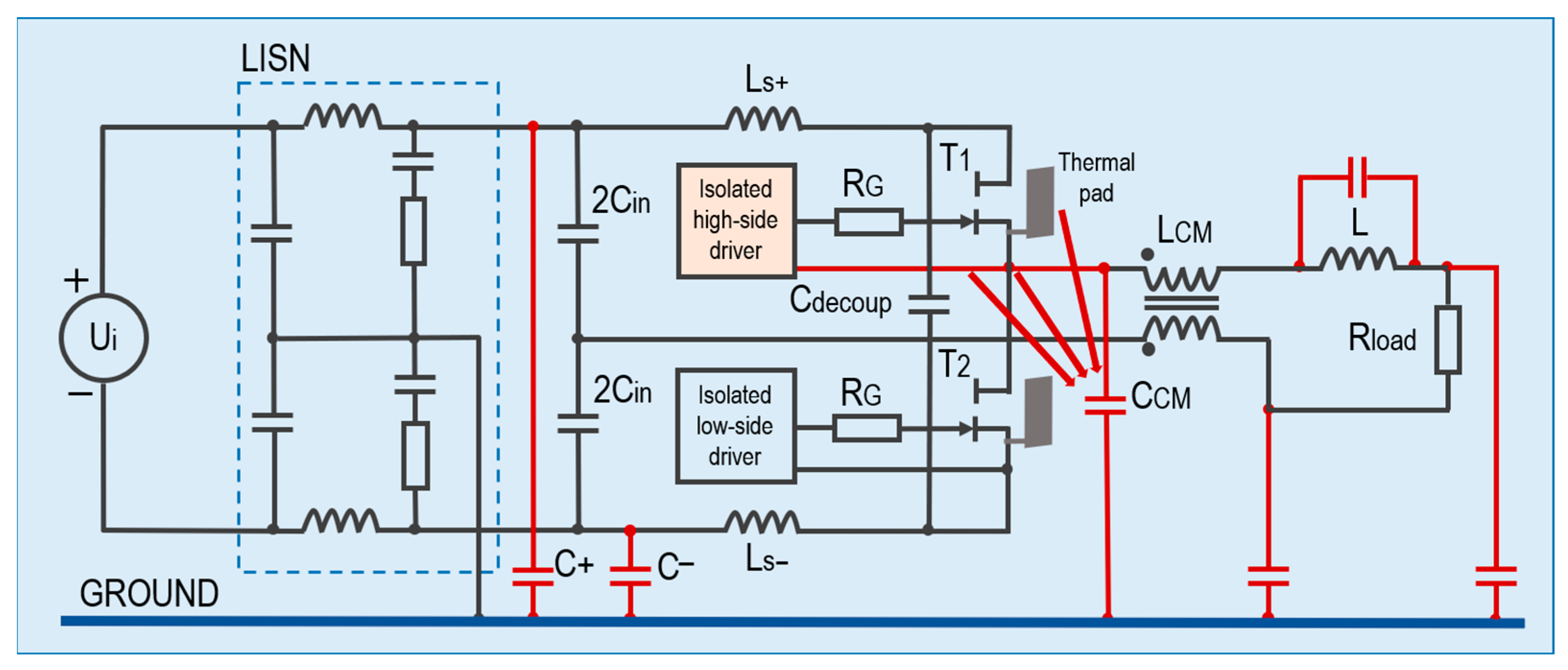
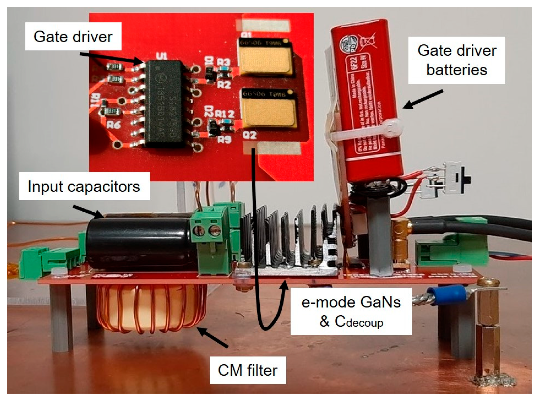
4.7. Experimental Validation
5. Conclusions
Author Contributions
Funding
Data Availability Statement
Acknowledgments
Conflicts of Interest
References
- Huang, A.Q. Power semiconductor devices for smart grid and renewable energy systems. Proc. IEEE 2019, 105, 2019–2047. [Google Scholar] [CrossRef]
- Buffolo, M.; Favero, D.; Marcuzzi, A.; De Santi, C.; Meneghesso, G.; Meneghini, M. Review and outlook on GaN and SiC power devices: Industrial state-of-the-art, applications, and perspectives. IEEE Trans. Electron Devices 2024, 71, 1344–1355. [Google Scholar] [CrossRef]
- Udabe, A.; Baraia-Etxaburu, I.; Garrido-Diez, D. Gallium nitride power devices: A state of the art review. IEEE Access 2023, 11, 48628–48650. [Google Scholar] [CrossRef]
- Baliga, B.J. Power semiconductors device figure of merit for high frequency applications. IEEE Electron Device Lett. 1989, 10, 455–457. [Google Scholar] [CrossRef]
- Huang, A.Q. New unipolar switching power device figures of merit. IEEE Electron Device Lett. 2004, 25, 298–301. [Google Scholar] [CrossRef]
- Global GaN Power Device Market Size Expecting to Reach USD 4,376 Billion in 2030, CAGR of 49%. Available online: https://www.trendforce.com/news/2024/08/16/news-global-gan-power-device-market-size-expected-to-reach-usd-4-376-billion-in-2030-cagr-of-49/ (accessed on 6 March 2025).
- GaN Power Semiconductors—2025 Predictions; Infineon Technologies AG: Neubiberg, Germany, 2025.
- Kozak, J.P.; Zhang, R.; Porter, M.; Song, Q.; Liu, J.; Wang, B.; Wang, R.; Saito, W.; Zhang, Y. Stability, reliability, and robustness of GaN power devices: A Review. IEEE Trans. Power Electron. 2023, 38, 8442–8471. [Google Scholar] [CrossRef]
- Method of Lifetime Estimation of EcoGaNTM in Soft Switching Applications. ROHM Semiconductors June 2024. Available online: https://fscdn.rohm.com/en/products/databook/white_paper/discrete/gan/hemt/method_of_lifetime_estimation_of_ecogan_in_soft-switching_operations_wp-e.pdf (accessed on 18 March 2025).
- Zhang, R.; Kozak, J.P.; Xiao, M.; Liu, J.; Zhang, Y. Surge-Energy and Overvoltage Ruggedness of P-Gate GaN HEMTs. IEEE Trans. Power Electron. 2020, 35, 13409–13419. [Google Scholar] [CrossRef]
- Wang, Z.; Nan, J.; Tian, Z.; Liu, P.; Wu, Y.; Zhang, J. Review on Main Gate Characteristics of P-Type GaN Gate High-Electron-Mobility Transistors. Micromachines 2024, 15, 80. [Google Scholar] [CrossRef]
- Fu, H.; Fu, K.; Chowdhury, S.; Palacios, T.; Zhao, Y. Vertical GaN Power Devices: Device Principles and Fabrication Technologies—Part I. IEEE Trans. Electron. Devices 2021, 68, 3200–3211. [Google Scholar] [CrossRef]
- Fu, H.; Fu, K.; Chowdhury, S.; Palacios, T.; Zhao, Y. Vertical GaN Power Devices: Device Principles and Fabrication Technologies—Part II. IEEE Trans. Electron. Devices 2021, 68, 3212–3222. [Google Scholar] [CrossRef]
- Langpoklakpam, C.; Liu, A.-C.; Hsiao, Y.-K.; Lin, C.-H.; Kuo, H.-C. Vertical GaN MOSFET Power Devices. Micromachines 2023, 14, 1937. [Google Scholar] [CrossRef] [PubMed]
- Ramanathan, D. Avalanche and short circuit robustness of vertical GaN FET. IEEE Power Electron. Mag. 2022, 9, 82–85. [Google Scholar] [CrossRef]
- Jones, E.A.; Wang, F.; Costinett, D. Review of commercial GaN power devices and GaN-based converter design challenges. IEEE J. Emerg. Sel. Top. Power Electron. 2016, 4, 707–719. [Google Scholar] [CrossRef]
- Iannaccone, G.; Sbrana, C.; Morelli, I.; Strangio, S. Power electronics based on wide-bandgap semiconductors: Opportunities and challenges. IEEE Access 2021, 9, 139446–139456. [Google Scholar] [CrossRef]
- Bay, O.; Tran, M.T.; El Baghdadi, M.; Chakraborty, S.; Hegazy, O. A Comprehensive Review of GaN-Based Bi-directional On-Board Charger Topologies and Modulation Methods. Energies 2023, 16, 3433. [Google Scholar] [CrossRef]
- Bau, P.; Cousineau, M.; Cougo, B.; Richardeau, F.; Rouger, N. CMOS active gate driver for closed-loop dv/dt control of GaN transistors. IEEE Trans. Power Electron. 2020, 35, 13322–13332. [Google Scholar] [CrossRef]
- Blank, M.; Glück, T.; Kugi, A.; Kreuter, H.P. Digital slew rate and S-shape control for smart power switches to reduce EMI generation. IEEE Trans. Power Electron. 2015, 30, 5170–5180. [Google Scholar] [CrossRef]
- Yatsugi, K.; Nomura, K.; Hattori, Y. Analytical technique for designing an RC snubber circuit for ringing suppression in a phase-leg configuration. IEEE Trans. Power Electron. 2018, 33, 4736–4745. [Google Scholar] [CrossRef]
- Yang, X.; Xu, M.; Li, Q.; Wang, Z.; He, M. Analytical method for RC snubber optimization design to eliminate switching oscillations of SiC. IEEE Trans. Power Electron. 2022, 37, 4672–4684. [Google Scholar] [CrossRef]
- Kim, J.; Shin, D.; Sul, S.K. A damping scheme for switching ringing of full SiC MOSFET by air core PCB circuit. IEEE Trans. Power Electron. 2018, 33, 4605–4615. [Google Scholar] [CrossRef]
- Yang, X.; Li, J.; Ding, Y.; Xu, M.; Zhu, X.-F.; Zhu, J. Observation of Transient Parity-Time Symmetry in Electronic Systems. Phys. Rev. Lett. 2022, 128, 065701. [Google Scholar] [CrossRef]
- Liu, T.; Chen, C.; Xu, K.; Zhang, Y.; Kang, Y. GaN-based megahertz single-phase inverter with a hybrid TCM control method for high efficiency and high-power density. IEEE Trans. Power Electron. 2018, 33, 4605–4615. [Google Scholar] [CrossRef]
- Oh, H.-S.; Hong, S.-Y.; Lee, J.; Lee, J.-B. Comparison of Bi-Directional Topologies for On-Board Charger: A 10.9 kW High-Efficiency High Power Density of DC-DCStage. Energies 2024, 17, 5496. [Google Scholar] [CrossRef]
- Dong, Z.; Yan, H.; Fan, Y.; Wu, X.; Zhang, J. A 3-D Integrated power module of GaN HEMTs based on silver sintering processes. IEEE Trans. Power Electron. 2024, 39, 2932–2937. [Google Scholar] [CrossRef]
- Moench, S.; Reiner, R.; Waltereit, P.; Benkhelifa, F.; Hückelheim, J.; Meder, D.; Zink, M.; Kaden, T.; Noll, S.; Mansfeld, S.; et al. PCB-embedded GaN-on-Si half-bridge and driver ICs with on-package gate. IEEE Trans. Power Electron. 2021, 36, 83–86. [Google Scholar] [CrossRef]
- Qi, Z.; Pei, Y.; Wang, L.; Yang, Q.; Wang, K. A highly integrated PCB embedded GaN full-bridge module with ultralow parasitic inductance. IEEE Trans. Power Electron. 2022, 37, 4161–4173. [Google Scholar] [CrossRef]
- Derkacz, P.B. EMC-Optimized Converter Using Power GaN Devices. Ph.D. Thesis, University Grenoble Alpes, Saint-Martin-d’Hères, France, Gdansk University of Technology, Gdańsk, Poland, 2024. [Google Scholar]
- Han, Z.; Li, X.; Ji, J.; Chen, L.; Wang, L.; Cheng, Z.; Yang, W.; You, S.; Li, Z.; Hao, Y.; et al. p-GaN Gate HEMTs on 6-Inch Sapphire by CMOS-Compatible Process: A Promising Game Changer for Power Electronics. IEEE Electron Device Lett. 2024, 45, 1257–1260. [Google Scholar] [CrossRef]
- Kassakian, J.G.; Perreault, D.J.; Verghese, G.C.; Schlecht, M.F. Principles of Power Electronics, 2nd ed.; Cambridge University Press: Cambridge, UK, 2024; pp. 528–530. [Google Scholar]
- GPIHV30SB5L Datasheet Version 3: Preliminary. GaNPower International Inc. Available online: https://iganpower.com/wp-content/uploads/2020/04/GPIHV30SB5L_V3.0.pdf (accessed on 6 March 2025).
- The Fundamental Advantages of Normally-off d-Mode GaN. Renesas Electronics. 2024. Available online: https://www.renesas.com/en/document/whp/fundamental-advantages-normally-d-mode-gan (accessed on 6 March 2025).
- Gupta, G.; Kanamura, M.; Swenson, B.; Bisi, D.; Romanczyk, B.; Neufeld, C.; Wienecke, S.; Ogino, T.; Miyazaki, Y.; Imanishi, K.; et al. 1200V GaN switches on sapphire substrate. In Proceedings of the IEEE 34th International Symposium on Power Semiconductor Devices and ICs (ISPSD), Vancouver, BC, Canada, 22–25 May 2022. [Google Scholar]
- Brohlin, P.L.; Ramadass, Y.K.; Kaya, C. Direct-Drive Configuration for GaN Devices. Texas Instruments Inc. 2018. Available online: https://www.ti.com/lit/wp/slpy008a/slpy008a.pdf (accessed on 6 March 2025).
- Huber, J.; Kolar, J.W. Monolithic bidirectional power transistors. IEEE Power Electron. Mag. 2023, 10, 28–38. [Google Scholar] [CrossRef]
- NV6428 Datasheet. Navitas Semiconductor Ltd. Available online: https://navitassemi.com/wp-content/plugins/gb-navitas-stock-checker/product_files/NV6428_70mO%20Max_Bi-Directional%20GaNFast_TOLT.pdf (accessed on 18 March 2025).
- Nain, N.; Walser, S.; Huber, J.; Leong, K.K.; Kolar, J.W. Self-reverse-blocking (SRB) control of dual-gate monolithic bidirectional GaN switch with quasi-ohmic on-state characteristic. IEEE Trans. Power Electron. 2022, 37, 10091–10094. [Google Scholar] [CrossRef]
- Does GaN Have a Body Diode?—Understanding the Third Quadrant Operation of GaN; Application Report SNOAA3; Texas Instruments Inc.: Singapore, 2019; Available online: https://www.ti.com/lit/an/snoaa36/snoaa36.pdf (accessed on 18 March 2025).
- Hamdaoui, Y.; Michler, S.; Bidaud, A.; Ziouche, K.; Medjdoub, F. 1200-V fully vertical GaN-on-Silicon p-i-n diodes with avalanche capability and high on-state current above 10 A. IEEE Trans. Electron Devices 2025, 72, 338–343. [Google Scholar] [CrossRef]
- Stevens, J.; Ribarich, T.; Oliver, S. Practical realization of GaN’s capability. IEEE Power Electron. Mag. 2022, 9, 56–63. [Google Scholar] [CrossRef]
- Lindow, A. Gallium nitride integration: Braking down technical barriers quickly. IEEE Power Electron. Mag. 2020, 7, 56–63. [Google Scholar] [CrossRef]
- Lai, R.; Zhou, Z.; Wu, J.; Dai, Y.; Liu, X.; Zhang, B.; Shi, Y.; Li, S.; Qin, Z. A Monolithic GaN power stage with common-mode transient immunity and negative voltage operation design for high-frequency power converters. IEEE Trans. Power Electron. 2024, 39, 8129–8145. [Google Scholar] [CrossRef]
- Integrated Power Stage (IPS) IGI60F1414A1L. Infineon Technologies AG. Available online: https://www.infineon.com/cms/en/product/power/gallium-nitride/gallium-nitride-transistor/igi60f1414a1l/?redirId=295083 (accessed on 18 March 2025).
- Persson, E. Optimizing PCB layout for HV GaN power transistors. IEEE Power Electron. Mag. 2023, 10, 65–78. [Google Scholar] [CrossRef]
- Regnat, G.; Jeannin, P.-O.; Frey, D.; Ewanchuk, J.; Mollov, S.W.; Ferrieux, J.-P. Optimized Power Modules for Silicon Carbide MOSFET. IEEE Trans. Ind. Appl. 2018, 54, 1634–1644. [Google Scholar] [CrossRef]
- GN001 Application Guide. Design with GaN Enhancement Mode HEMT. GaN System Inc. 2018. Available online: https://gansystems.com/wp-content/uploads/2018/04/GN001-Design_with_GaN_EHEMT_180412.pdf (accessed on 6 March 2025).
- Derkacz, P.B.; Schanen, J.-L.; Jeannin, P.-O.; Musznicki, P.; Chrzan, P.J.; Petit, M. 3D PCB package for GaN inverter leg with low EMC feature. In Proceedings of the EPE’20 ECCE Europe, Lyon, France, 7–11 September 2020. [Google Scholar]
- Derkacz, P.B.; Schanen, J.-L.; Jeannin, P.-O.; Chrzan, P.J.; Musznicki, P.; Petit, M. EMI mitigation of GaN power inverter leg by local shielding techniques. IEEE Trans. Power Electron. 2022, 37, 11996–12004. [Google Scholar] [CrossRef]
- Wang, J.; Burgos, R.; Boroyevich, D.; Stewart, J.; Xu, J. Low Impedance Multi-Conductor Layered Bus Structure with Shielding. US 2020/0373254 A1. 26 November 2020.
- Fita, C.; Jeannin, P.-O.; Lefrance, P.; Clavel, E.; Delaine, J. A novel 3D structure for synchronous buck converter based on nitride Gallium transistors. In Proceedings of the IEEE Energy Conversion Congress and Exposition (ECCE), Milwaukee, WI, USA, 18–22 September 2016. [Google Scholar]


| Material | HMFOM | HCAFOM | HTFOM |
|---|---|---|---|
| Si | 1.00 | 1.00 | 1.00 |
| 4H-SiC | 5.26 | 31.99 | 0.47 |
| GaN | 11.56 | 96.67 | 0.12 |
| Device | Manufacturer | RDS(on) [mΩ] | QG [nC] | VGS(th) [V] | IGSS [mA] | Topology |
|---|---|---|---|---|---|---|
| IGT65R025D2 | Infineon | 25 | 11 | 0.9–1.6 | 46 | GIT 1 |
| GS0650605BA | GaN Systems | 25 | 14 | 1.1–2.6 | 0.32 | p-GaN |
| INN650TA030AH | Innoscience | 26 | 16 | 1.2–2.5 | 0.25 | p-GaN |
| Device | Manufacturer | RDS(on) [mΩ] | QG [nC] | VGS(th) [V] | ID/IDM [A] | Topology |
|---|---|---|---|---|---|---|
| TP65H035G4QS | Renesas | 35 | 22 | 4 | 46/240 | Cascode |
| GAN039650NBB | Nexperia | 33 | 26 | 3.9 | 58/234 | Cascode |
| LMG3522R030 | Texas Inst. | 26 | - | - | 55/125 | Direct drive |
| Device | Manufacturer | RDS(on) [mΩ] | QOSS [nC] | VDS [V] | ID/IDM [A] | Topology |
|---|---|---|---|---|---|---|
| NV6428 | Navitas | 52 | 100 | 650 | 49/78 | Dual gate |
| INV120EQ035A | Innoscience | 3.5 | 95 | 120 | 100/320 | Single gate |
| GANB4R8-040 | Nexperia | 4 | 12.2 | 40 | 20/100 | Single gate |
| Device | Manufacturer | RDS(on) [mΩ] | dv/dt [V/ns] | VDS [V] | ID/IDM [A] | Topology |
|---|---|---|---|---|---|---|
| BM3G005MUVLB | ROHM | 50 | 150 | 650 | 21/68 | Single HEMT |
| NV6522 | Navitas | 40 | 100 | 650 | 41/83 | Single HEMT |
| EPC2152 | EPC | 2 × 10 | - | 80 | 15/- | Half-bridge |
| IGI60F1414A1L | Infineon | 2 × 140 | 300 | 600 | 6/23 | Half-bridge |
| Layout | 2D | 2.5D | 3D |
|---|---|---|---|
| Stray inductance @ 1 MHz | 8.9 nH | 7.56 nH | 1.93 nH |
| Stray inductance @ 10 MHz | 4.83 nH | 4.69 nH | 1.49 nH |
| Stray inductance @ 100 MHz | 6.94 nH | 5.46 nH | 1.57 nH |
Disclaimer/Publisher’s Note: The statements, opinions and data contained in all publications are solely those of the individual author(s) and contributor(s) and not of MDPI and/or the editor(s). MDPI and/or the editor(s) disclaim responsibility for any injury to people or property resulting from any ideas, methods, instructions or products referred to in the content. |
© 2025 by the authors. Licensee MDPI, Basel, Switzerland. This article is an open access article distributed under the terms and conditions of the Creative Commons Attribution (CC BY) license (https://creativecommons.org/licenses/by/4.0/).
Share and Cite
Chrzan, P.J.; Derkacz, P.B. GaN Power Transistors in Converter Design Techniques. Energies 2025, 18, 2890. https://doi.org/10.3390/en18112890
Chrzan PJ, Derkacz PB. GaN Power Transistors in Converter Design Techniques. Energies. 2025; 18(11):2890. https://doi.org/10.3390/en18112890
Chicago/Turabian StyleChrzan, Piotr J., and Pawel B. Derkacz. 2025. "GaN Power Transistors in Converter Design Techniques" Energies 18, no. 11: 2890. https://doi.org/10.3390/en18112890
APA StyleChrzan, P. J., & Derkacz, P. B. (2025). GaN Power Transistors in Converter Design Techniques. Energies, 18(11), 2890. https://doi.org/10.3390/en18112890