Article

A Power Decoupling Control Strategy for Multi-Port Bidirectional Grid-Connected IPT Systems

by
Xuewei Pan
1,
Peiwen Ma
1,
Zhouchi Cai
1 and
Danyang Bao
1,2,*
1
School of Robotics and Advanced Manufacturing, Harbin Institute of Technology, Shenzhen 518055, China
2
School of Mechanical and Electrical Engineering, Shenzhen Polytechnic University, Shenzhen 518107, China
*
Author to whom correspondence should be addressed.
Energies 2025, 18(10), 2589; https://doi.org/10.3390/en18102589
Submission received: 19 March 2025 / Revised: 12 May 2025 / Accepted: 13 May 2025 / Published: 16 May 2025
(This article belongs to the Special Issue Voltage/Frequency/Power Quality Monitoring and Control in Smart Grids)

Abstract

In the context of vehicle-to-grid (V2G) applications, single-port bidirectional inductive power transfer (BDIPT) systems have difficulty coping with the growing demand for electric vehicles. This paper proposes a multi-port BDIPT system based on an LCC-LCC compensation network. A multi-phase-shift (MPS) control with more degrees of freedom is proposed, where the external phase shift angle controls the power transmission direction and the internal phase shift angle controls the transmitted power magnitude. Independent multi-port operation for the multi-port BDIPT system can be achieved. Finally, the theoretical results are verified by experiments. The experimental results show that the LCC-LCC-based multi-port BDIPT system can achieve independent control of the transmission power at each port.

1. Introduction

Wireless power transfer (WPT) technology has received widespread attention for its flexibility, convenience, safety, and reliability. It has been widely used in biomedical applications [1], electric vehicles (EVs) [2,3,4], etc. WPT technology is mainly divided into capacitive power transfer (CPT) and inductive power transfer techniques (IPT). The CPT technique utilizes an alternating electric field to transfer power wirelessly. Dai and Ludois [5] compared inductive and capacitive power transfer for small air-gap applications, highlighting the limitations of low coupling capacitance and high voltage stress on capacitive couplers. Rozario et al. [6] evaluated compensation networks in small air-gap and large air-gap applications, recommending LLC resonant designs for small air-gap CPT (flexible, low parasitic effects) and double-sided LCLC/LC networks for large air-gap CPT (with reduced voltage stress). However, CPT suffers from drawbacks, including high space occupation, increased cost, and the requirement of extra circuitry, as well as control and design complexity. IPT has been received more research attention and can be classified into unidirectional inductive power transfer (UDIPT) [7,8], and BDIPT [9,10]. Most of the current research focuses on UDIPT systems. With the introduction of the V2G concept, the BDIPT system is beginning to show its unique advantages. Under the V2G application scenario, EVs can be used as energy storage devices to supply energy to the grid. Previous research mainly focuses on single-port BDIPT systems [11,12,13]. However, as the number of devices increases, there is no doubt that multi-port BDIPT systems will become an important development in WPT technology.
Compared with single-port BDIPT systems, multi-port BDIPT systems are more complex in terms of structure and control. There are four basic compensation networks—including series-series (S-S), series-parallel (S-P), parallel-series (P-S), and parallel-parallel (P-P)—and two higher order compensation networks, including LCL-LCL and LCC-LCC [14]. Symmetrical compensation networks are preferred for their multi-port structure. In [15], a BDIPT system adopts the S-S compensation network. However, when mutual inductance is reduced, overcurrent may occur in the primary coil. An LCL-LCL compensation network is used in [16,17]. Ref. [16] presents the transmission characteristics and steady-state performance of LCL-LCL compensation networks. Ref. [17] analyzes the transmission characteristics of the BDIPT system based on LCL-LCL compensation network. It was found that the coil current of this system has independent current source characteristics. When the mutual inductance decreases or even disappears, the coil current remains unchanged and the system still works in a safe operating condition, unlike the S-S compensation network. However, the transmission power capacity of this system is much smaller than that of the S-S compensation network. Refs. [10,12,18] improve the LCL-LCL compensation network and propose an LCC-LCC compensation network. Compared with the LCL-LCL compensation network, the LCC-LCC compensation network adds a series resonance capacitor. It inherits the advantages of the LCL-LCL compensation network even while the system transmission power is much larger, which is more suitable for applications in multi-port BDIPT systems. In addition, LCC-LCC compensation networks have become the preferred solution for high-power wireless charging (such as electric vehicles and industrial equipment) due to their anti-offset capabilities, load independence, high efficiency, and soft switching characteristics [19,20]. Although its parameter design complexity is high, the optimized design of an LCC-LCC compensation network can significantly improve the robustness and adaptability of the system, especially suitable for applications with strict requirements for reliability and efficiency. In [21], a parameter offline tuning method was achieved by switching the parallel-compensated capacitance for a detuned LCC–LCC resonant converter to alleviate the power drop caused by the coupling variation.
For multi-port BDIPT systems, there exists cross-coupling phenomenon between each port, resulting in coupled power. The presence of coupled power increases the interaction between the ports and has an impact on the system’s transmission power. In order to improve the reliability of the independent operation of multi-port systems, it is necessary to achieve multi-port decoupling control. In [22,23], the power control of the multi-port BDIPT systems is achieved through cascading a DC-DC converter after the secondary rectifier bridge. However, the cascaded DC-DC converter is a two-stage structure, which increases system complexity and power loss. Another control method is variable frequency control; Ref. [24] analyzed the frequency characteristics of the LCC-LCC compensation network and achieved constant voltage and current output characteristics of the system at two different resonant frequencies. However, the frequency adjustable range of this control is limited, and the variable frequency control makes the system less flexible. Moreover, due to the phenomenon of frequency splitting [25], this control strategy can have an impact on the system’s efficiency. In [26], the full-bridge and half-bridge modes are combined to maintain high efficiency while also ensuring ZVS for the LCC-LCC compensated WPT system. The ZVS soft-switching under the symmetric phase-shift (SPS) control is not fully accurate. Under SPS control, due to the maximum amplitude of the fundamental output voltage of the primary and secondary full-bridge converters, the amplitude of the resonant current on both sides is also high, resulting in significant power loss.
To solve the above problem, this paper proposes a multi-port BDIPT system based on an LCC-LCC compensation network using MPS control. The structure of this paper is as follows: Section 2 models the multi-port BDIPT system and analyzes the system transmission power characteristics under the multiple-phase-shift control method. In Section 3, different power decoupling methods are proposed under different external phase angle cases. Then, a harmonics-based time-domain model of the multi-port BDIPT system is built to analyze the soft switching range of switches, and finally, a multi-port power closed-loop control strategy under power decoupling is proposed. In Section 4, simulation and experimental verification are carried out. Section 5 provides the conclusion.

2. Multi-Port BDIPT System Modeling and Analysis

In this section, a three-port BDIPT system is used as an example to model a multi-port BDIPT system based on an LCC-LCC compensation network and to analyze the system’s transmission power characteristics under an MPS control.

2.1. Model of the Multi-Port BDIPT System

The proposed multi-port BDIPT system schematic is shown in Figure 1. Each port consists of a DC voltage source, a full-bridge converter, a compensation network, and a coil, which can either provide power as an input source or absorb power as a load, enabling power flow between the multi-ports. As shown in Figure 1, port 1 is connected to the dc-bus, which is represented by voltage Vdp. The DC bus is the rectified output from the grid through the bidirectional AC/DC circuit. Port 2 and port 3 are considered to be connected to EVs, which are also equivalent to DC bus voltages Vds1 and Vds2. vAB, vCD, and vEF are the high frequency AC output voltages generated by the full-bridge converters from Vdp, Vds1, and Vds2, respectively; iAB, iCD, and iEF are the output currents of the full-bridge converters at each port. Sn1Sn4 (port numbers n = 1, 2, 3) are the power switches of each port’s full-bridge converters, respectively. Lp, Ls1, and Ls2 are the self-inductances of each coil. L1, C1, and Cp are the compensation components of port 1’s coil; L2, C2, and Cs1 and L3, C3, and Cs2 are the compensation components of port 2 and port 3’s coils. M12 and M13 are the mutual inductances of the port 1 and port 2 or port 3 coils; M23 are the mutual inductances of the port 2 and port 3 coils. The output voltages are measured across the output capacitors Co1 and Co2, and the output currents are measured between the output capacitors Co1 and Co2 and the batteries Vds1 and Vds2. When the power is transferred from port 1 to ports 2 and 3, the H-bridge of port 1 serves as the inverter while the H-bridges of ports 2 and 3 serve as the rectifier. The rectification mechanism of the H-bridge is explained as follows. Taking the H-bridge of port 2 as an example, when the secondary current iCD is positive, the switch pair S23 and S22 are conducting. The iCD flows to the output capacitor and the battery load through S23 and S22. When the secondary current iCD is negative, the switch pair S21 and S24 are conducting. The iCD flows to the output capacitor and the battery load through S21 and S24. In this way, the alternating current iCD is rectified into DC form. In the reverse direction, the H-bridge of port 1 serves as the rectifier. The operating principle is the same.
Assuming that the parameters of the system are symmetrical, to make the system fully compensated, the switching frequency of the switches is set to be the same as the resonant frequency of the LCC-LCC compensation network. ω is the general angular frequency and ωs is defined as the resonant angular frequency when the system is fully compensated. Under the fully compensated condition, the parameters of the LCC-LCC compensation network satisfy Equation (1).
{ ω s L p 1 ω s C p = 1 ω s C 1 = ω s L 1 ω s L s 1 1 ω s C s 1 = 1 ω s C 2 = ω s L 2 ω s L s 2 1 ω s C s 2 = 1 ω s C 3 = ω s L 3
The output voltage of each port’s full-bridge converter can be expressed through the Fourier Series Expansion, which is shown in (2). βs1 and βs2 are the internal phase shift angles of the port 2 and port 3 full-bridge converters, respectively. δ1 and δ2 are the phases between  U ˙ AB , 1 and  U ˙ CD , 1  or  U ˙ EF , 1 , respectively, also known as external phase shift angles.
{ ν A B ( t ) = 4 V d p π   n = 1,3 , 1 n cos n ω t sin n π 2 ν C D ( t ) = 4 V d s 1 π n = 1,3 ,   1 n cos n ω t n δ 1 sin n β s 1 2 ν E F ( t ) = 4 V d s 2 π n = 1,3 , 1 n cos ( n ω t n δ 2 ) sin ( n β s 2 2 )
Since the resonant frequency used in the design of the EVs’ WPT system is the same as the switching frequency, the loosely coupled transformer is usually wound with multi-strand litz wires and the parasitic resistance of the coil is small, so the resonance compensation network shows high impedance to the higher harmonics and the high harmonic component has less influence on the system. To simplify the analysis, the fundamental harmonic approximation (FHA) method is used. The simplified model is shown in Figure 2, where the fundamental components of the output voltage of each full-bridge converter are equivalent to sinusoidal AC bus voltage.
In Figure 2 U ˙ AB , 1 U ˙ CD , 1 , and  U ˙ EF , 1  are the fundamental components of the output voltages of the three-port full-bridge converter;  I ˙ AB , 1 I ˙ CD , 1 , and  I ˙ EF , 1  are the fundamental components of the output current of each port’s full-bridge converter—that is, the resonant inductor currents of each port—and their directions are non-correlated with the corresponding output voltage;  I ˙ p I ˙ s 1 , and  I ˙ s 2  are the coil currents of each port, with the positive direction of flow to the coils; r1r3 are the parasitic resistances of each coil, characterizing the losses caused by the coils.
U ˙ ps U ˙ sp 1 , and  U ˙ sp 2  are the induced voltages between the ports, equivalent to the current control voltage sources, the expression of which are given by
U ˙ ps = j ω s M 12 I ˙ s 1 + j ω s M 12 I ˙ s 2 U ˙ sp 1 = j ω s M 12 I ˙ p + j ω s M 23 I ˙ s 2 U ˙ sp 2 = j ω s M 13 I ˙ p + j ω s M 23 I ˙ s 1
where the mutual inductance of M12, M13, and M23 can be expressed as a function of the coupling coefficient kij (i, j = 1~3, ij).
M 12 = k 12 L p L s 1 M 13 = k 13 L p L s 2 M 23 = k 23 L s 1 L s 2
Taking  U ˙ AB , 1  as a reference, the fundamental components  U ˙ AB , 1 U ˙ CD , 1 , and  U ˙ EF , 1  are shown in (5), where the value range of the external phase shift angles is −π ≤ δn ≤ π, and the value range of the internal shifted phase angles is 0 ≤ βsn ≤ π (n = 1, 2).
U ˙ AB , 1 = 2 2 π V dp sin ( π 2 ) U ˙ CD , 1 = 2 2 π V ds 1 sin ( β s 1 2 ) δ 1 U ˙ EF , 1 = 2 2 π V ds 2 sin ( β s 1 2 ) δ 2
According to Kirchhoff’s voltage and current laws and the simplified model shown in Figure 2, considering the losses caused by the coils, the equations for each loop are shown in (6).
U ˙ AB , 1 U ˙ CD , 1 U ˙ EF , 1 0 0 0 = X 1 0 0 X 7 X A X B 0 X 2 0 X A X 8 X C 0 0 X 3 X B X C X 9 X 4 0 0 X 4 + X 7 X A X B 0 X 5 0 X A X 5 + X 8 X C 0 0 X 6 X B X C X 6 + X 9 I ˙ AB , 1 I ˙ CD , 1 I ˙ EF , 1 I ˙ p I ˙ s 1 I ˙ s 2
where, XA, XB, and XC are the phasor expression of each mutual inductance and X1 to X9 are the equivalent impedances of each loop, as shown in (7).
X A = j ω s M 12 X B = j ω s M 13 X C = j ω s M 23 X n = j ω s L n ( n = 1 ~ 3 ) X m = 1 j ω s C m - 3 ( m = 4 ~ 6 ) X 7 = j ω s L p + 1 j ω s C p + r 1 X 8 = j ω s L s 1 + 1 j ω s C s 1 + r 2 X 9 = j ω s L s 2 + 1 j ω s C s 2 + r 1
The substitution of (1) in (6) yields resonant inductor currents  I ˙ AB , 1 I ˙ CD , 1 , and  I ˙ EF , 1 , and coil currents  I ˙ p I ˙ s 1 , and  I ˙ s 2  expressions for each port.
I ˙ AB , 1 I ˙ CD , 1 I ˙ EF , 1 I ˙ p I ˙ s 1 I ˙ s 2 = r 1 ( ω s L 1 ) 2 j M 12 ω s L 1 L 2 j M 13 ω s L 1 L 3 j M 12 ω s L 1 L 2 r 2 ( ω s L 2 ) 2 j M 23 ω s L 2 L 3 j M 13 ω s L 1 L 3 j M 23 ω s L 2 L 3 r 3 ( ω s L 3 ) 2 1 j ω s L 1 0 0 0 1 j ω s L 2 0 0 0 1 j ω s L 3 U ˙ AB , 1 U ˙ CD , 1 U ˙ EF , 1
The coil currents are only related to the equivalent voltage source of their corresponding ports, independent of other ports, and exhibit independent current source characteristics. The magnitude of the resonant inductor current at each port is affected by the equivalent voltage source of all ports.
Considering the loss resistances and multiplying the conjugate value of the resonant inductor current of each port with the fundamental component of the output voltage of the corresponding port full-bridge converter, the transferred active power and reactive power can be given as (9) to (14), shown below.
P 1 = Re U ˙ AB , 1 I ˙ AB , 1 * = 8 V dp π 2 ω L 1 [ M 12 L 2 V ds 1 sin ( β s 1 2 ) sin ( δ 1 ) + M 13 L 3 V ds 2 sin ( β s 2 2 ) sin ( δ 2 ) + r 1 V dp ω L 1 ]
P 2 = Re U ˙ CD , 1 I ˙ CD , 1 * = 8 π 2 [ M 12 ω L 1 L 2 V dp V ds 1 sin ( β s 1 2 ) sin ( δ 1 ) + M 23 ω L 2 L 3 V ds 1 V ds 2 sin ( β s 1 2 ) sin ( β s 2 2 ) sin ( δ 1 δ 2 ) + r 2 V ds 1 2 ω 2 L 2 2 sin 2 ( β s 1 2 ) ]
P 3 = Re U ˙ EF , 1 I ˙ EF , 1 * = 8 π 2 [ M 13 ω L 1 L 3 V dp V ds 2 sin ( β s 2 2 ) sin ( δ 2 ) + M 23 ω L 2 L 3 V ds 1 V ds 2 sin ( β s 1 2 ) sin ( β s 2 2 ) sin ( δ 2 δ 1 ) + r 3 V ds 2 2 ω 2 L 3 2 sin 2 ( β s 2 2 ) ]
Q 1 = Im U ˙ AB , 1 I ˙ AB , 1 * = 8 V dp π 2 ω L 1 [ M 12 L 2 V ds 1 sin ( β s 1 2 ) cos ( δ 1 ) + M 13 L 3 V ds 2 sin ( β s 2 2 ) cos ( δ 2 ) ]
Q 2 = Im U ˙ CD , 1 I ˙ CD , 1 * = 8 V ds 1 π 2 ω L 2 [ M 12 L 1 V dp sin ( β s 1 2 ) cos ( δ 1 ) + M 23 L 3 V ds 2 sin ( β s 1 2 ) sin ( β s 2 2 ) cos ( δ 1 δ 2 ) ]
Q 3 = Im U ˙ EF , 1 I ˙ EF , 1 * = 8 V ds 2 π 2 ω L 3 [ M 13 L 1 V dp sin ( β s 2 2 ) cos ( δ 2 ) + M 23 L 2 V ds 1 sin ( β s 1 2 ) sin ( β s 2 2 ) cos ( δ 2 δ 1 ) ]
As shown in Figure 2, the output voltage and the current direction of each port are non-correlated reference directions, so when the active power Pn > 0 (n = 1, 2, 3), it indicates that port n provides power, and when Pn < 0, power flow is reversed; when the reactive power Qn > 0, it indicates that port n provides inductive reactive power, and when Qn < 0, port n provides capacitive reactive power.

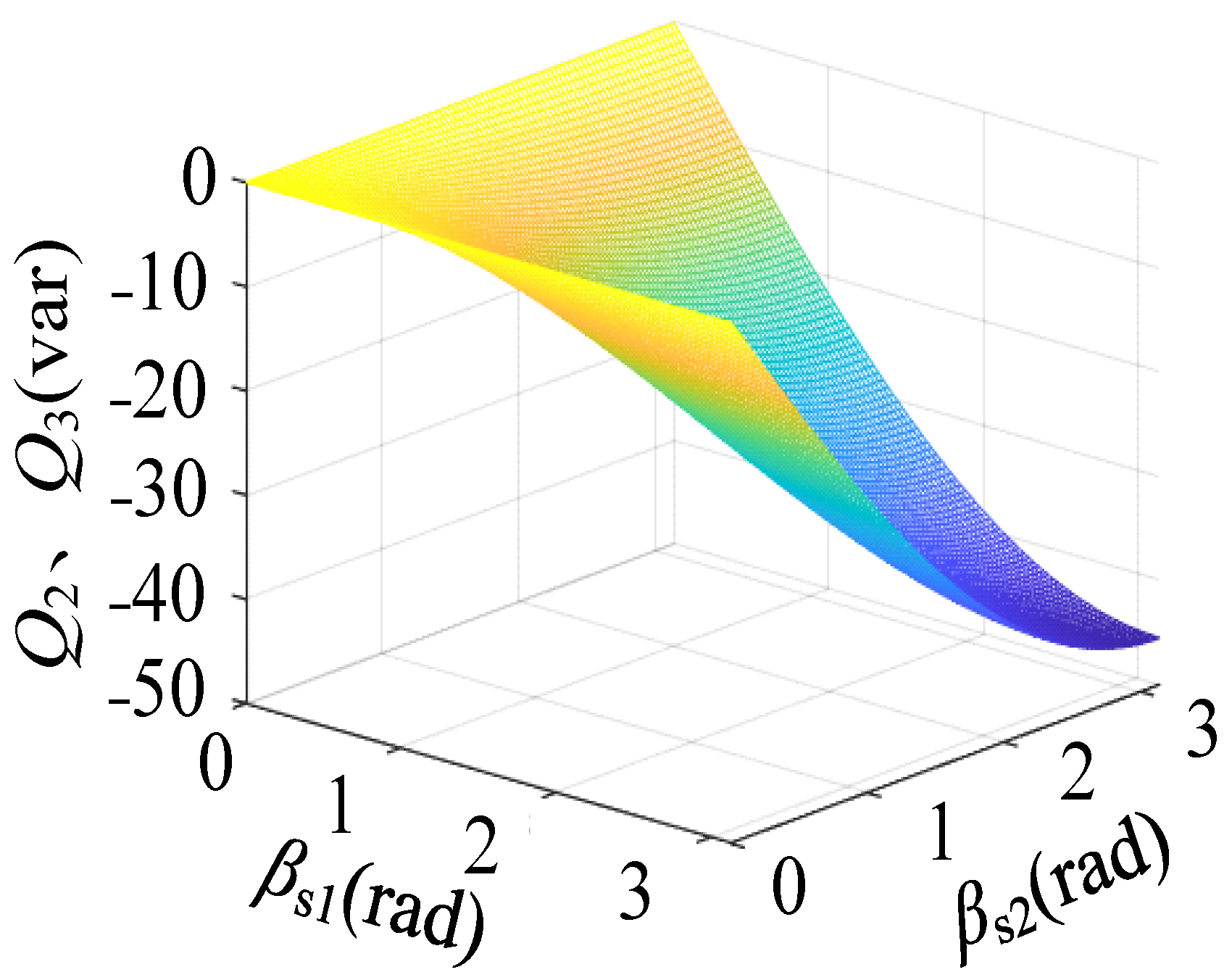
2.2. Analysis of the System Transmission Power Characteristics

Since the traditional single-phase-shift control has a single control variable, it is difficult for it to control the power flow of a multi-port BDIPT system. This paper adopts a MPS control with more control variables, including four control variables—namely, the two internal phase shift angles βs1 and βs2—and two external phase shift angles, δ1 and δ2. The control signals of the power switches and the output voltage of each port full-bridge converter are shown in Figure 3.
In Figure 3, in each full-bridge converter, the upper and lower switches of the same bridge leg that operate with 180° complementary conduction, and the diagonal switches are turned on or off at the same time with a duty cycle of 0.5. Sn1Sn4 are the switches of port n full-bridge (n = 1, 2, 3). For example, for port 1, the upper switch S11 and the lower switch S12 exhibit 180° complementary conduction, while the diagonal switches S11 and S13 are turned on or off at the same time. There exists a phase shift between port 1 and ports 2 and 3: namely, the external phase shift angles δ1 and δ2. S11 switches ON before S21 with a leading phase angle δ1, and before S31 with a leading phase angle δ2. There exists a phase shift within port 2 and port 3, namely, the two internal phase shift angles βs1 and βs2. S23 switches ON leading S21 with βs1, and S33 switches ON leading S31 with βs2.
From Equations (9)–(11), it can be found that the active power of each port is related to the fundamental amplitude of the output voltage of all full-bridge converters, meaning that power flows between ports. Taking δ1 = δ2 as an example, when δ1 > 0 and δ2 > 0, and P1 > 0, P2 < 0, and P3 < 0, power is transferred from port 1 to port 2 and port 3; when δ1 < 0 and δ2 < 0, and P1 < 0, P2 > 0, and P3 > 0, power flow is reversed. When δ1 = δ2 = ±90°, the relationships between the active power of each port and the internal phase shift angles βs1 and βs2 are shown in Figure 4. From Equation (12), the reactive power Q1 of port 1 is zero, and from Equations (13) and (14), the expressions of the reactive powers Q2 and Q3 of port 2 and port 3 are equal, so the relationship between Q2 and Q3 and βs1 and βs2 can be as shown in Figure 5.
As shown in Figure 4, when δ1 = δ2 = 90°, power is transferred from port 1 to port 2 and port 3; when δ1 = δ2 = −90°, the power flow is reversed. In the bidirectional transmission of power, the transmission power of each port is determined by the internal phase shift angles. As seen in Figure 5, Q2 and Q3 change with different combinations of βs1 and βs2. When βs1 and βs2 are both π, Q2 and Q3 are the largest; when βs1 and βs2 are both zero, Q2 and Q3 are also zero. Obviously, Q2 and Q3 decrease as βs1 and βs2 decrease.
In summary, the external phase shift angles δ1 and δ2 determine the direction of the power flow of the multi-port BDIPT system, and the internal phase shift angles βs1 and βs2 determine the magnitude of the power flow and the reactive power under MPS control.

3. Proposed Power Decoupling and Power Control Strategy

In the previous section, a multi-port BDPT system model is established. There exists a cross coupling between ports 2 and 3 that creates a power flow that prevents multi-port BDIPT systems from operating independently. In this section, the power decoupling of the multi-port is carried out by the MPS control, so that each port can operate independently. The soft switching characteristics of each port and the system transmission power are analyzed on the basis of power decoupling. Finally, a MPS closed-loop control strategy is proposed to control the direction and magnitude of the power flow based on the power decoupling and wide soft switching range.

3.1. Power Decoupling

In Figure 2, it can be seen that port 2 and port 3 are cross-coupled, generating induced voltage. The coupled power will flow between the two receiving ports and cannot operate independently. Figure 6 shows the power transmission of the multi-port BDIPT system after power decoupling. Through analysis of the power transmission characteristics in the multi-port BDIPT system, it is found that the external phase shift angles δ1 and δ2 are used to control the direction of power flow when MPS control is adopted. Therefore, this section explores methods to achieve power decoupling under MPS control and analyzes two cases in which δ1 and δ2 are either equal or unequal.
When δ1 = δ2, based on Equations (10) and (11), the transmission power expression for port 2 and port 3 can be divided into three parts. The rewritten equations can be expressed as
P 2 = P 2 _ 1 + P 2 _ 2 + P 2 _ 3 P 3 = P 3 _ 1 + P 3 _ 2 + P 3 _ 3
where,
P 2 _ 1 = M 12 ω s L 1 L 2 U ˙ AB , 1 U ˙ CD , 1 sin ( δ 1 ) P 3 _ 1 = M 13 ω s L 1 L 3 U ˙ AB , 1 U ˙ EF , 1 sin ( δ 2 ) P 2 _ 2 = M 23 ω s L 2 L 3 U ˙ CD , 1 U ˙ EF , 1 sin ( δ 2 δ 1 ) P 3 _ 2 = M 23 ω s L 2 L 3 U ˙ CD , 1 U ˙ EF , 1 sin ( δ 1 δ 2 ) P 2 _ 3 = r 2 U ˙ CD , 1 2 ( ω s L 2 ) 2 P 3 _ 3 = r 3 U ˙ EF , 1 2 ( ω s L 3 ) 2
Under the conditions of fixed working frequency, coil self-inductance, and mutual inductance, P2 is taken as an example. From Equation (16), P2_1 is related to the fundamental amplitude values of the output voltages at port 1 and port 2 (| U ˙ AB , 1 |, | U ˙ CD , 1 |) and δ1, and is independent of any parameters of port 3. P2_2 is related to | U ˙ CD , 1 |, | U ˙ EF , 1 |, and (δ2δ1). P2_3 is only related to | U ˙ CD , 1 |, which represents the loss caused by parasitic resistance in the coil of that port. Port 3 follows the same principles.
When power is transmitted forward, port 2 and port 3 respectively receive power from port 1, the magnitudes of which are denoted by P2_1 and P3_1. At the same time, the coupling power between port 2 and port 3, which is transmitted due to cross-coupling, is characterized by P2_2 and P3_2. From the equations for P2_2 and P3_2, it can be observed that by controlling the external phase shift angles δ1 and δ2 such that the difference (δ1δ2) is zero, i.e., δ1 = δ2, the coupling power can be made zero, thereby achieving power decoupling.
When δ1δ2, port 2 and port 3 have different phase differences with respect to port 1, meaning that there is a phase difference between the output voltages vCD and vEF of the full-bridge converter at port 2 and port 3. From Equations (15) and (16), it can be inferred that there is power transmitted between port 2 and port 3, which complicates independent control.
Based on the analysis carried out in Section 2, it can be concluded that the port with a leading phase outputs power to the outside, while the port with a lagging phase receives power. There is no power transmission between ports with the same phase. Therefore, it is necessary to control the internal phase shift angles βs1 and βs2 of port 2 and port 3, respectively, to ensure that the phase difference between port 2 and port 3 is zero, which can achieve power decoupling between the two ports. At this point, the output voltage waveforms of each port are as shown in Figure 7.
As seen in Figure 7, according to the phase relationship, the relationship between external phase shift angles δ1 and δ2 and internal phase shift angles βs1 and βs2 under this condition can be derived as follows:
2 ( δ 2 δ 1 ) = β s 2 β s 1
From equation (17), when δ1δ2, βs1βs2.

3.2. Analysis of System Transmission Power Regulation

Based on the power decoupling of the multi-port BDIPT system, the system power transmission can be divided into three cases: (a) each port transmits the same power; (b) each port transmits different power; (c) a port transmits zero power.
When δ1 = δ2, the degrees of freedom of the MPS are δ1 (δ2), βs1, and βs2, respectively. From Equations (10) and (11), it can be seen that the power transferred between port 2 and port 3 is zero. According to the decoupled power transmission expressions, the relationships between the transmitted power of each port and βs1 and βs2 are shown in Figure 8.
Taking the forward energy transmission as an example, at this time, port 1 is the transmitter, and ports 2 and 3 are the receivers. As shown in Figure 8, the magnitudes of P2 and P3 correspond one-to-one with the combination of βs1 and βs2, and increase with the increase in βs1 and βs2. P1 reaches its maximum.
When βs1 = βs2 = π, P2 and P3 also correspond one-to-one with the βs1 and βs2, respectively, and are almost positively linearly related. Therefore, when δ1 = δ2, the internal phase shift angles βs1 and βs2 are selected. The multi-port BDIPT system decides the direction of power transmission by controlling the positive and negative of the external phase shift angles δ1 and δ2, while δ1 = δ2 = ±90° to minimize the reactive power of the system. The magnitudes of the internal phase shift angles βs1 and βs2 are used to control the magnitude of the power transmitted by each port, so that each port can transmit the same power or different power. When δ1 = δ2, the magnitude of the power transmitted by ports 2 and 3 can be independently controlled by the internal phase shift angle βs1 = βs2, respectively. Simple PI controllers are employed to control the power transferring capacity of each port while the positive and negative of the external phase shift angle δ1 = δ2 controls the power transferring direction, as shown in Figure 1.
When δ1δ2, the degrees of freedom of the multiphase shift control are δ1, δ2, βs1, and βs2. In order to achieve power decoupling, δ1, δ2, βs1, and βs2 need to satisfy Equation (17), while the internal phase shift angle satisfies βs1βs2. As shown in Equations (10), (11), and (17), the four degrees of freedom is reduced to three. To simplify the control, this section fixes the outward phase shift angle δ1 to analyze the system’s transmission power, which is known from Equation (17); at this time, the outward phase shift angle δ2 = 0.5 (βs1βs2) + δ1.
As the positive or negative value of the outward phase shift angle determines the direction of power transmission, when δ2 > 0, δ1 > −0.5 (βs1βs2), i.e., δ1 ≥ max {−0.5 (βs1βs2)} = π/2, at this time δ1 > 0 and δ2 > 0, energy is transmitted in the positive direction; similarly, when δ2 < 0, δ1 ≤ min {−0.5 (βs1βs2)} = −π/2, at this time energy is transmitted in the negative direction. According to the above discussion, the outward phase shift angle δ1 can be taken as π/2 ≤ |δ1| ≤ π, while the outward phase shift angle can be taken as |δ2| ≤ π.
When δ1 = 90° according to Equation (17) and δ2 > 0, the power is transmitted in the positive direction; the relationships between the transmitted power of each port and βs1 and βs2 are shown in Figure 8. As shown in Figure 8, P1 is related to both βs1 and βs2, varying valley-like with the internal phase shift angle and reaching a maximum value in the middle part at βs1 = βs2 = π and a minimum value all around at βs1 = 0 and βs2 = π, respectively. The minimum value is non-zero due to the consideration of the losses generated by the coil parasitic resistance. In Figure 8b, the variation of βs2 has very little effect on P2 because δ1 is fixed, illustrating that P2 is almost exclusively related to βs1 when δ1 is fixed. In Figure 8c, P3 at port 3 is curved around βs1 = 0 because P3 is only related to βs2 and varies sinusoidally with βs2, reaching a minimum around βs2 = π/2. This means that P3 is related to the βs1 and βs2 when δ1 is fixed.
As stated above, when δ1δ2, different power transmission situations can be achieved by changing βs1 and βs2. However, under this condition, power decoupling is achieved by adjusting βs1 and βs2 to make the phase difference between vCD and vEF zero. Changing both βs1 and βs2 while fixing a certain external phase shift angle will result in a significant change in the transmission power of the other port with the variation of βs1 and βs2, as shown in P3 of Figure 8c. Therefore, a more complicated control strategy is needed to adjust the multi-port transmission power when δ1δ2.

4. Experimental Verification

For experimental validation, a multi-port BDIPT system is built, as shown in Figure 9. The system specifications are given in Table 1. The loosely coupled transformer is composed of three flat circular coils with different diameters. To reduce the effects of the skin effect and proximity effect, the coils are all wound with Litz copper wire. To simulate electric vehicle charging, the large coil connected to port 1 on the grid side is placed at the bottom and has the largest diameter. The coils connected to ports 2 and 3 on the electric vehicle side are small coils with the same structure, with their centers located on the same horizontal line. Cree silicon carbide power MOSFET C2M0080120D is chosen for the switches of each full-bridge converter. The control chip adopts TMS320F28335. The current sensing circuit adopts the current sensor CKSR 25-NP, and the sampled signal is sent to DSP after filtering.

4.1. The Experimental Verification of Power Decoupling

To verify the effectiveness of the proposed power decoupling, experiments with different external phase shift angles are carried out. The DC bus voltage and current waveforms of port 2 and port 3 before and after power decoupling are shown in Figure 10 and Figure 11, where Vds1 and Vds2 are the DC bus voltages of port 2 and port 3 and Ids1 and Ids2 are the DC currents of port 2 and port 3, respectively.
As shown in Figure 10a, when changing Vds2 from 25 V to 50 V, Ids2 remains unchanged. Vds1 decreases by 13% and Ids1 remains unchanged, which indicates that there is cross-coupling between port 2 and port 3, and the change in the power transmission at port 3 affects the power transmission at port 2.
As shown in Figure 10b,c, when changing Vds2 from 25 V to 50 V, Vds1 and Ids1 remain unchanged under the proposed decoupling control. This indicates that power decoupling has been achieved between port 2 and port 3 under different external phase shift angles. This also verifies the effectiveness of multi-port power decoupling.

4.2. The Experimental Verification of the System Power Transmission Characteristics

Under MPS control, the external phase shift angles are used to control the direction of the power flow while the internal phase shift angles are used to control the magnitude of the power flow. To verify the role of different phase shift angles in system power transmission control, the output voltage and current of the full-bridge converters at each port under different operating conditions are shown in Figure 11 and Figure 12.
When δ1 = δ2, in order to achieve maximum power transmission and minimum reactive power, the external phase shift angles satisfy |δ1| = |δ2| = 90°. When δ1 = δ2 = 90°, power is transmitted from port 1 to port 2 and port 3; at this point, power is transmitted in the forward direction. The DC voltage sources of the three ports are set to 40 V.
When βs1 = βs2 = 180°, the output voltage waveforms of all ports’ full-bridge converters are as shown in Figure 11a, and the output voltage and current waveforms of all ports’ bridges are as given in Figure 11b,c; at this time, the system is in the maximum transmission power condition.
As shown in Figure 11a, it can be seen that the phase of the full-bridge inverter output voltage VAB of port 1 is ahead of the VCD of port 2 and the VEF of port 3, and their phase difference is 90°. As shown in Figure 11b,c, it can be seen that the full-bridge inverter output voltage and current of port 1 are in phase, while the full-bridge inverter output voltage and current of port 2 and port 3 are opposite in phase, indicating that port 1 is transmitting power to ports 2 and 3. At this time, the DC output current Idp of port 1 is 6.92 A, and the maximum transmission power P1 of port 1 is 276.8 W. The P2 of port 2 and P3 of port 3 are 117.2 W and 126.8 W, respectively.
Keeping the DC source voltage and mutual inductance of each port constant, βs1 remains at 180° and βs2 changes from 180° to 150°. The experimental waveforms of output voltages and currents of all ports’ bridges are shown in Figure 12.
As shown in Figure 12, compared with βs1 = βs2 = 180°, P3 decreases with the decrease in the effective values of the full-bridge inverter output voltage VEF and current IEF of port 3. Since it is in the power decoupling state at this time, the change in P3 does not affect the magnitude of P2. At this time, the DC output current Ids1 of port 1 is 6.49 A, and the transmission power P1 is 259.6 W. P2 is 110 W and P3 is 104.6 W, which represents a decrease of 17.5% compared to the condition of βs1 = βs2 = 180°.
Keeping the mutual inductance of each port constant, Figure 13, Figure 14, Figure 15 and Figure 16 show the waveforms of the system during the reverse power flow under δ1 = δ2 = −90°. At this time, Vds1 = 40 V and Vds2 = Vds3 = 20 V. When βs1 = βs2 = 180°, the output voltage waveforms of all ports’ full-bridge converters are as shown in Figure 13a, and the output voltage and current waveforms of all ports’ bridges are as given in Figure 13b,c. As can be seen in Figure 13a, VAB is clearly lagging behind VCD and VEF. In Figure 13b,c, it can be seen that the full-bridge inverter output voltage and current of port 1 are in opposite in phase, while the full-bridge inverter output voltages and currents of port 2 and port 3 are in phase. This indicates that the power flow is from port 2 and port 3 to port 1. The DC output currents Ids1 of port 2 and Ids2 of port 3 are −3.14 A and −3 A, respectively, with corresponding transmission powers P2 and P3 of −62.8 W and −59.97 W; P1 is −108.2 W.
Keeping the DC source voltage and mutual inductance of each port constant, when βs1 changes from 180° to 150° and βs2 changes from 180° to 120°, the experimental waveforms of output voltages and currents of all ports’ bridges are as shown in Figure 14. As can be seen, compared to βs1 = βs2 = 180°, P2 and P3 decrease, indicating a decrease in the effective values of the output voltage VCD and current ICD of the full-bridge converters at port 2 and port 3. At this moment, the Ids1 of port 2 and Ids2 of port 3 are −2.6 A and −2.41 A, respectively, with corresponding transmission powers P2 and P3 of −52 W and −48.2 W; P1 is −81.3 W. The difference between P1 and the sum of P2 and P3 is due to the loss of the system. Compared to the transmission powers of βs1 = βs2 = 180°, P2 and P3 decrease by 17.2% and 19.6%, respectively.
When δ1δ2, if δ1 = 90° and δ2 is always greater than zero, the power is transmitted in the forward direction. On the other hand, if δ1 = −90° and δ2 is always less than zero, the power is transmitted in the reverse direction. The DC voltage sources of the three ports are set to 40 V. Figure 15 shows the output voltage and current waveforms of the system during the forward power flow under δ1 = 90°, βs1 = 180°, and βs2 = 150°. From Figure 15a, it can be seen that the phase of VAB leads to that of VEF. Also, from Figure 15b, the phase difference between VCD and VEF is zero, indicating that VAB leads to both VCD and VEF. At this moment, Idp is 6.78 A, P1 is 271.11 W, and P2 and P3 are 143 W and 92.75 W, respectively.
Keeping the mutual inductance of each port constant, when δ1 = −90°, βs1 = 150°, and βs2 = 180°, power is transmitted from ports 2 and 3 to port 1. At this time, Vdp = 40 V and Vds1 = Vds2 = 20 V. The experimental waveforms of the output voltages and currents of each full-bridge converter at each port are shown in Figure 16. From Figure 16a, it can be seen that VAB lags behind VCD. Moreover, as seen in Figure 16b, the phase difference between VCD and VEF is zero, which indicates that VAB lags behind both VCD and VEF. At this moment, the Ids1 of port 2 and Ids2 of port 3 are −2.84 A and −3.24 A, respectively, with transmission powers of −56.88 W and −64.8 W; P1 is −101.6 W.
The experimental results above are consistent with the theoretical analysis presented earlier, which verifies the following: (1) controlling the external phase shift angles δ1 and δ2 between ports can control the direction of power flow, and (2) controlling the internal phase shift angles βs1 and βs2 of ports 2 and 3 can change the magnitude of power flow based on power decoupling. Moreover, the smaller the internal phase shift angles, the smaller the power flow.

4.3. The Experimental Verification of Closed-Loop Power Control Strategy

To verify the effectiveness of the closed-loop power control strategy under MPS control, the DC voltage sources at each port are fixed at 40 V. When the system operates stably, the DC current reference values Ids1_ref and Ids2_ref for ports 2 and 3 are switched, and the corresponding DC output current at each port is stabilized at the reference value through a closed-loop current control algorithm, thereby achieving closed-loop power control.
When Ids1_ref is changed from 2 A to 1.5 A, it means that P2 is switched from 80 W to 60 W. Meanwhile, Ids2_ref is kept at 2 A, maintaining P3 at 80 W. The experimental waveforms of the DC voltages Vds1 and Vds2 and currents Ids1 and Ids2 of ports 2 and 3 are shown in Figure 17. It is can be seen that Ids1 is decreased from 2 A to 1.5 A while Vds1 remains at 40 V, resulting in a decrease in P2 from 80 W to 60 W. Vds2 and Ids2 remain constant, and P3 remains at 80 W. Figure 18 shows the experimental waveforms of the DC voltages and currents at ports 2 and 3 when Ids1_ref is decreased from 2 A to 1.5 A and Ids2_ref is decreased from 3 A to 1 A, resulting in a decrease in P2 from 80 W to 60 W and in P3 from 120 W to 40 W, respectively. As can be seen, Ids1 is decreased from 2 A to 1.5 A, while Vds1 remains at 40 V, resulting in a decrease in P2 from 80 W to 60 W. Meanwhile, Vds2 remains unchanged while Ids2 is decreased from 3 A to 1 A, resulting in a decrease in P3 from 120 W to 40 W. From Figure 17 and Figure 18, the effectiveness of the closed-loop power control strategy is verified, which indicates that the transmission power of each port can be independently controlled by the internal phase shift angles of the corresponding port.

5. Conclusions

In this paper, a multi-port BDIPT system based on an LCC-LCC compensation network is built, and a power decoupling method is proposed. By modeling a multi-port bidirectional wireless charging system, an MPS control scheme with more degrees of freedom and flexibility is designed. With the proposed MPS control, the direction of power flow is controlled by the polarity of the external phase shift angles, and the magnitude of power flow is controlled by the magnitude of the internal phase shift angles. A prototype of the BDIPT system is built to verify the theoretical analysis. The experimental waveforms are consistent with the theoretical derivation, and power decoupling among multiple ports has been achieved under different lead-lag phase angles. Based on the power decoupling, the power transmission of each port can be independently controlled.

Author Contributions

Conceptualization, X.P.; methodology, X.P.; software, P.M.; validation, P.M. and Z.C.; formal analysis, D.B.; investigation, P.M.; writing—original draft preparation, P.M.; writing—review and editing, D.B.; visualization, Z.C.; supervision, X.P.; project administration, X.P.; funding acquisition, X.P. All authors have read and agreed to the published version of the manuscript.

Funding

This research was funded by Guangdong Basic and Applied Basic Research Foundation (Grant Number: 2025A1515010037), Key Field Special Projects of Guangdong Province Department of Education (Grant Number: 6024210069K), and Shenzhen Fundamental Research Program (Grant Number: GJHZ20220913143008016).

Data Availability Statement

All data included in this study are available upon request by contact with the corresponding author.

Conflicts of Interest

The authors declare no conflict of interest.

References

  1. Chen, Q.; Wong, S.C.; Tse, C.K.; Ruan, X. Analysis, design, and control of a transcutaneous power regulator for artificial hearts. IEEE Trans. Biomed. Circuits Syst. 2009, 3, 23–31. [Google Scholar] [CrossRef] [PubMed]
  2. Bosshard, R.; Kolar, J.W. All-SiC 9.5 kW/dm3 on-board power electronics for 50 kW/85 kHz automotive IPT system. IEEE Trans. Emerg. Sel. Top. Power Electron. 2017, 5, 419–431. [Google Scholar] [CrossRef]
  3. Guo, Y.; Wang, L.; Zhu, Q.; Liao, C.; Li, F. Switch-on modeling and analysis of dynamic wireless charging system used for electric vehicles. IEEE Trans. Ind. Electron. 2016, 63, 6568–6579. [Google Scholar] [CrossRef]
  4. Feng, H.; Cai, T.; Duan, S.; Zhao, J.; Zhang, X.; Chen, C. An LCC compensated resonant converter optimized for robust reaction to large coupling variation in dynamic wireless power transfer. IEEE Trans. Ind. Electron. 2016, 63, 6591–6601. [Google Scholar] [CrossRef]
  5. Dai, J.; Ludois, D.C. A survey of wireless power transfer and a critical comparison of inductive and capacitive coupling for small gap applications. IEEE Trans. Power Electron. 2015, 30, 6017–6029. [Google Scholar] [CrossRef]
  6. Rozario, D.; Azeez, N.A.; Williamson, S.S. Comprehensive review and comparative analysis of compensation networks for capacitive power transfer systems. In Proceedings of the 2016 IEEE 25th International Symposium on Industrial Electronics (ISIE), Santa Clara, CA, USA, 8–10 June 2016; pp. 823–829. [Google Scholar]
  7. Tavakoli, R.; Pantic, Z. Analysis, design and demonstration of a 25-kW dynamic wireless charging system for roadway electric vehicles. IEEE Trans. Emerg. Sel. Top. Power Electron. 2018, 6, 1378–1393. [Google Scholar] [CrossRef]
  8. Dai, X.; Li, X.; Li, Y.; Hu, A.P. Impedance-matching range extension method for maximum power transfer tracking in IPT system. IEEE Trans. Power Electron. 2018, 33, 4419–4428. [Google Scholar] [CrossRef]
  9. Madawala, U.K.; Thrimawithana, D.J. A bidirectional inductive power interface for electric vehicles in V2G systems. IEEE Trans. Ind. Electron. 2011, 58, 4789–4796. [Google Scholar] [CrossRef]
  10. Zhang, X.; Cai, T.; Duan, S.; Feng, H.; Hu, H.; Niu, J.; Chen, C. A Control Strategy for Efficiency Optimization and Wide ZVS Operation Range in Bidirectional Inductive Power Transfer System. IEEE Trans. Ind. Electron. 2019, 66, 5958–5969. [Google Scholar] [CrossRef]
  11. Cao, L.; Bao, J.; Loo, K.-H.; Pan, X.; Zhang, R. A hybrid control strategy for dynamic compensation of cross-coupling effect in two-load IPT system. IET Power Electron. 2023, 16, 1943–1957. [Google Scholar] [CrossRef]
  12. Li, G.; Pan, X.; Bao, D.; Cai, Z.; Kumar, A. A novel noncommunication-based inductive power transfer control technique for battery charging application. IET Power Electron. 2025, 18, e12837. [Google Scholar] [CrossRef]
  13. Mohamed, A.A.S.; Berzoy, A.; de Almeida, F.G.N.; Mohammed, O. Modeling and Assessment Analysis of Various Compensation Topologies in Bidirectional IWPT System for EV Applications. IEEE Trans. Ind. Appl. 2017, 53, 4973–4984. [Google Scholar] [CrossRef]
  14. Li, G.; Cai, Z.; Feng, C.; Sun, Z.; Pan, X. DAB-Based Bidirectional Wireless Power Transfer System with LCC-S Compensation Network under Grid-Connected Application. Energies 2024, 17, 4519. [Google Scholar] [CrossRef]
  15. Jiang, Y.; Wang, L.; Fang, J.; Zhao, C.; Wang, K.; Wang, Y. A Joint Control with Variable ZVS Angles for Dynamic Efficiency Optimization in Wireless Power Transfer System. IEEE Trans. Power Electron. 2020, 35, 11064–11081. [Google Scholar] [CrossRef]
  16. Tang, Y.; Chen, Y.; Madawala, U.K.; Thrimawithana, D.J.; Ma, H. A New Controller for Bidirectional Wireless Power Transfer Systems. IEEE Trans. Power Electron. 2018, 33, 9076–9087. [Google Scholar] [CrossRef]
  17. Liu, C.; Ge, S.; Guo, Y.; Li, H.; Cai, G. Double-LCL resonant compensation network for electric vehicles wireless power transfer: Experimental study and analysis. IET Power Electron. 2016, 9, 2262–2270. [Google Scholar] [CrossRef]
  18. Li, W.; Zhao, H.; Deng, J.; Li, S.; Mi, C.C. Comparison Study on SS and Double-Sided LCC Compensation Topologies for EV/PHEV Wireless Chargers. IEEE Trans. Veh. Technol. 2016, 65, 4429–4439. [Google Scholar] [CrossRef]
  19. Li, J.; Zhang, X.; Tong, X. Research and Design of Misalignment-Tolerant LCC–LCC Compensated IPT System with Constant-Current and Constant-Voltage Output. IEEE Trans. Power Electron. 2023, 38, 1301–1313. [Google Scholar] [CrossRef]
  20. Peng, J.; Zhang, B.; Su, W. A Hybrid Control Strategy of LCC–LCC Compensated Electric Vehicles Wireless Charging System with Wide ZVS Range. IEEE Trans. Power Electron. 2025, 40, 6282–6295. [Google Scholar] [CrossRef]
  21. Deng, J.; Mao, Q.; Wang, W.; Li, L.; Wang, Z.; Wang, S.; Guidi, G. Frequency and Parameter Combined Tuning Method of LCC–LCC Compensated Resonant Converter with Wide Coupling Variation for EV Wireless Charger. IEEE J. Emerg. Sel. Top. Power Electron. 2022, 10, 956–968. [Google Scholar] [CrossRef]
  22. Fu, M.; Ma, C.; Zhu, X. A Cascaded Boost–Buck Converter for High-Efficiency Wireless Power Transfer Systems. IEEE Trans. Ind. Inform. 2014, 10, 1972–1980. [Google Scholar] [CrossRef]
  23. Zhang, K.; Ye, T.; Yan, Z.; Song, B.; Hu, A.P. Obtaining Maximum Efficiency of Inductive Power-Transfer System by Impedance Matching Based on Boost Converter. IEEE Trans. Transp. Electrif. 2020, 6, 488–496. [Google Scholar] [CrossRef]
  24. Vu, V.-B.; Tran, D.-H.; Choi, W. Implementation of the Constant Current and Constant Voltage Charge of Inductive Power Transfer Systems with the Double-Sided LCC Compensation Topology for Electric Vehicle Battery Charge Applications. IEEE Trans. Power Electron. 2018, 33, 7398–7410. [Google Scholar] [CrossRef]
  25. Liu, X.; Yuan, X.; Xia, C.; Wu, X. Analysis and Utilization of the Frequency Splitting Phenomenon in Wireless Power Transfer Systems. IEEE Trans. Power Electron. 2021, 36, 3840–3851. [Google Scholar] [CrossRef]
  26. Fu, N.; Deng, J.; Wang, Z.; Wang, W.; Wang, S. A hybrid mode control strategy for LCC–LCC-compensated WPT system with wide ZVS operation. IEEE Trans. Power Electron. 2022, 37, 2449–2460. [Google Scholar] [CrossRef]
Figure 1. Schematic diagram of the multi-port BDIPT system with an LCC-LCC compensation network.
Energies 18 02589 g001
Figure 2. Simplified FHA model of the multi-port BDIPT system.
Energies 18 02589 g002
Figure 3. MPS control of the multi-port BDIPT system.
Energies 18 02589 g003
Figure 4. Relationship between the active power of each port and βs1 and βs2 under MPS control (δ1 = δ2). (a) Port 1. (b) Port 2. (c) Port 3.
Energies 18 02589 g004
Figure 5. Relationship between the reactive power of port 2 and port 3 and βs1 and βs2 under MPS control (δ1 = δ2).
Energies 18 02589 g005
Figure 6. Schematic diagram of power transmission mode of the multi-port BDIPT system after power decoupling. (a) Forward power transmission. (b) Reverse power transmission.
Energies 18 02589 g006
Figure 7. Schematic diagram of output voltages for each port when δ1δ2.
Energies 18 02589 g007
Figure 8. Relationships between the active power of each port and βs1 and βs2 under MPS control (δ1δ2). (a) Port 1. (b) Port 2. (c) Port 3.
Energies 18 02589 g008
Figure 9. Prototype multi-port bidirectional BDIPT system.
Energies 18 02589 g009
Figure 10. The DC voltage and current waveforms of port 2 and 3. (a) Before power decoupling. (b) After power decoupling (δ1 = δ2). (c) After power decoupling (δ1 ≠ δ2).
Energies 18 02589 g010
Figure 11. The experimental waveforms of all ports full-bridge under βs1 = βs2 = 180° (forward power transmission). (a) Output voltage of all ports. (b) Output voltage and current of port 1. (c) Output voltage and current of port 2 and port 3.
Energies 18 02589 g011
Figure 12. Output voltage and current waveforms of all ports’ bridges under βs1 = 180° and βs2 = 150° when δ1 = δ2 (forward power transmission). (a) Port 1 and port 3. (b) Port 2 and port 3.
Energies 18 02589 g012
Figure 13. The experimental waveforms of all ports’ full-bridges under βs1 = βs2 = 180° (reverse power transmission). (a) Output voltage of all ports. (b) Output voltage and current of port 1 and port 3. (c) Output voltage and current of port 2 and port 3.
Energies 18 02589 g013
Figure 14. Output voltage and current waveforms of all ports’ full-bridge converters under βs1 = 150° and βs2 = 120° (reverse power transmission). (a) Port 1 and port 3. (b) Port 2 and port 3.
Energies 18 02589 g014
Figure 15. Output voltage and current waveforms of all ports’ full-bridge converters under βs1 = 180° and βs2 = 150° when δ1δ2 (forward power transmission). (a) Port 1 and port 3. (b) Port 2 and port 3.
Energies 18 02589 g015
Figure 16. Output voltage and current waveforms of all ports’ full-bridge converters under βs1 = 150° and βs2 = 180° (reverse power transmission). (a) Port 1 and port 2. (b) Port 2 and port 3.
Energies 18 02589 g016
Figure 17. The DC voltages and current waveforms of ports 2 and 3 with the closed-loop power control strategy (only changing P2).
Energies 18 02589 g017
Figure 18. The DC voltages and current waveforms of ports 2 and 3 with the closed-loop power control strategy (changing P2 and P3).
Energies 18 02589 g018
Table 1. Specifications of the proposed multi-port BDIPT system for experiments.
SymbolParametersValue
fSwitching frequency85 kHz
LpPort 1 coil inductance122 μH
L1Port 1 compensation inductance14.6 μH
C1Port 1 parallel compensation capacitor233.4 nF
CpPort 1 series compensation capacitor34.01 nF
Ls1Port 2 coil inductance50 μH
L2Port 2 compensation inductance15 μH
C2Port 2 parallel compensation capacitor233.1 nF
Cs1Port 2 series compensation capacitor100.3 nF
Ls2Port 3 coil inductance50 μH
L3Port 3 compensation inductance15.2 μH
C3Port 3 parallel compensation capacitor233.3 nF
Cs2Port 3 series compensation capacitor100.5 nF
M12Mutual inductance between port 1&211.72 μH
M13Mutual inductance between port 1&311.72 μH
M23Mutual inductance between port 2&37.5 μH
Disclaimer/Publisher’s Note: The statements, opinions and data contained in all publications are solely those of the individual author(s) and contributor(s) and not of MDPI and/or the editor(s). MDPI and/or the editor(s) disclaim responsibility for any injury to people or property resulting from any ideas, methods, instructions or products referred to in the content.

