Article

An Improved Single-Phase Multiple DC Source Inverter Topology for Distributed Energy System Applications

1
Department of Electrical Engineering, Z.H. College of Engineering & Technology, Aligarh Muslim University, Aligarh 202001, India
2
Power Electronics, Machines and Control Research Centre, University of Nottingham, Nottingham NG7 2RD, UK
3
High-Power Converter Systems (HLU), Technical University of Munich (TUM), 80333 Munich, Germany
4
Electrical Engineering Department, Faculty of Engineering, Assiut University, Assiut 71516, Egypt
5
Center for Energy Transition, Universidad San Sebastián, Santiago 8420524, Chile
6
Faculty of Electrical Engineering, Universiti Teknologi Malaysia UTM, Johor Bharu 81310, Malaysia
*
Authors to whom correspondence should be addressed.
Energies 2024, 17(9), 2146; https://doi.org/10.3390/en17092146
Submission received: 21 March 2024 / Revised: 20 April 2024 / Accepted: 25 April 2024 / Published: 30 April 2024

Abstract

:
This work presents an improved structure of a single-phase muti-input multilevel inverter (MIMLI) for distributed energy resources, which is capable of producing a nine-level output in symmetric mode and 21 levels in asymmetrical mode. The topology uses four DC sources and ten switches, with four switches being bidirectional and the remaining unidirectional. The operation of the circuit is analyzed in an asymmetrical mode, and switching signals are accomplished using the Nearest Level Control (NLC) PWM technique. Depending on the value of the DC sources used, the number of levels can vary. In this work, different DC source algorithms were also proposed, and the analysis of the inverter has been carried out considering the algorithms producing the maximum number of levels. The inverter was simulated in MATLAB/Simulink under steady state and dynamic conditions, achieving a 3.89% THD in output. The thermal analysis was conducted using PLECS software 4.1.2 to assess losses and efficiency. A laboratory prototype of the proposed topology was developed and tested, confirming its performance through simulation results and proving it economically viable for medium- and high-power applications.

1. Introduction

The integration of interface converters in environmentally friendly distributed energy resources (DERs) is crucial for delivering high-efficiency, reliable, and high-quality electric power. A DC/AC power processing interface is needed to meet grid standards. Advancements in semiconductor technologies and power electronic techniques have led to the introduction of multilevel inverters (MLIs) to limit the constraints of standard two- or three-level inverters, offering advantages such as reduced voltage stress, higher efficiency, and less electromagnetic interference [1,2]. MLIs are popular due to their high-quality output voltage at a nominal cost. Researchers aim to reduce inverter costs by using overall components effectively and conforming to IEEE 519 [3] guidelines. MLIs are useful in high-power UPS, traction drives, renewable energy integration, and aircraft [4,5].
Conventional multilevel inverters (MLI) such as cascaded H-Bridge (CHB), Neutral Point Clamped (NPC-MLI), and Flying Capacitors (FC-MLI) are widely used in current systems due to their modularity and ease of control [6]. However, they are disadvantaged due to the high number of power switches required to obtain multiple voltage levels and the complexity of voltage control mechanisms. The large switch count in the converter system makes it bulky, costly, and complex due to its inclusion of gate driver, protection, and heat sink units [7,8]. Reducing power switch count is a growing research area in MLIs. The literature presents many topologies of MLIs to address these issues, categorized into symmetric and asymmetric. Symmetric topologies offer equal magnitude of DC sources, simplified control, and high modularity; but they necessitate additional semiconductor devices for improved power quality [9,10]. In asymmetric topologies, DC sources are of different magnitude, producing higher voltage levels with a reduced device but losing modularity and increasing switching stress on switches [11,12].
The topology in [13] uses three asymmetrical DC sources to provide 55 output voltage levels, but uses 44 switches and seven capacitors. Consequently, the number of devices is still high, and the capacitors require a complicated control mechanism. To reduce complexity, the authors of [14] developed a topology without capacitors. Nevertheless, the increased device count and switching stress are due to the need for an additional H-Bridge to create negative levels. Another asymmetric topology was introduced by the authors of [15], which resulted in a significant reduction in switching stress but an increase in device count. The authors of [16] suggested a topology with fewer devices, but an H-Bridge was needed to achieve negative levels. The H-Bridge switches must tolerate all DC sources, increasing the total standing voltage (TSV) and cost.
The author proposed a nine-level output unit in [17], which can be extended to provide 25-level output, with seven DC sources and 10 switches, six of which are bidirectional. The topology in [18] utilized isolated DC sources and bidirectional switches to reach appropriate output voltage levels, although the voltage stress was significant. The structure proposed in [19] utilizes a basic unit of a cascading H-bridge circuit, which employs 10 switches and three DC sources to provide a 13-level output. More components are required if more units are added to reach the desired levels, increasing the cost. Another MLI topology proposed in [20] generates voltage levels and polarity separately, requiring more DC sources and increased costs. The author of [21] developed a ladder-shaped topology for higher voltage levels with fewer devices but faced issues with a separate polarity generation unit, leading to increasing cost and less reliability. A new topology in [22] for renewable energy applications provides seven levels of output voltage in a symmetrical mode and 11 levels in an asymmetrical mode using six unidirectional and one bidirectional switch. This topology is extended for more voltage levels in cascaded connections. The modified MLI topology proposed in [23], featuring ten switches and four DC sources, achieves 21-level output, claiming modularity and impacting high-power quality. The authors in [24] introduce a novel inverter with a series cascade unit and bidirectional switches, which reduces overall blocking voltages and gate driver circuit requirements, reducing the failure rate of switches and allowing it for medium- and high-voltage applications.
Considering the above discussion, the aim is to develop a multilevel inverter with reduced device count, fewer On-state switches, and less blocking voltage; and operate in symmetrical and asymmetrical modes. This work proposes a multi-input multilevel inverter topology (MIMLI) for DERs, utilizing four DC sources and 10 switches; four of which are bidirectional and the rest are unidirectional. The topology operates in both symmetrical and asymmetrical modes, generating negative voltage levels inherently, reducing stress on switches, and improving inverter efficiency. The paper is organized as follows: Section 2 describes the proposed topology, which includes a circuit configuration, DC source selection, operation, switching technique, total standing voltage, and cost analysis. Section 3 discusses the simulation and experimental results for different loading conditions. The power loss and efficiency of the inverter are discussed in Section 4. Section 5 compares the proposed topology with other topologies. The application of the proposed topology is discussed in Section 6. Finally, Section 7 will conclude the work.

2. Description of the Proposed Topology

2.1. Circuit Configuration

The circuit configuration of the proposed topology is shown in Figure 1. It uses four DC sources and 10 semiconductor switches, four out of 10 switches are bidirectional, with two IGBTs coupled in a common emitter arrangement and fed by the same gate driver. The remaining switches are unidirectional. The proposed topology can be configured in symmetric and asymmetric configurations based on the magnitudes of the DC voltage sources V1, V2, V3, and V4. Energy storage, PV, batteries, and other renewable energy sources may be utilized as DC sources with a precise controller to maintain each voltage source at an appropriate level.

2.2. Proposed DC Source Selection Algorithm

The proposed topology generates nine levels at the output voltage in a symmetrical configuration, with equal magnitude for all DC sources. However, a symmetrical arrangement requires a large device count for higher voltage levels. To address this, an asymmetrical operation is needed. The topology may provide six distinct output levels by adjusting the magnitude of the DC source. The information on the magnitude of DC sources and the number of output voltage levels, ranging from nine to 21, is provided in Table 1. The performance of the proposed topology is considerably improved by selecting the proper magnitude of DC sources to generate higher voltage levels with reduced device count.

2.3. Operation of the Proposed Topology

The proposed topology generates 21 levels with fewer components. The DC sources are used in a ratio V1:V2:V3:V4 = 1:3:2:4, allowing for 10 positive, 10 negative, and zero levels at the output. Table 2 displays a topology’s switching modes and source combinations for an asymmetrical configuration, allowing for simplified switching. Switches in the conducting state have 1 against them, while the off state has 0. The conduction diagram for the positive half cycle is shown in Figure 2. Level 1V can be generated at the output by bringing V1 into the conduction path through S1, S3, and S9. Level 2V can be achieved by introducing V3 through S4, S5, and S8, or by V4-V3 source combination by turning on S1, S6, and S10. The voltage source V2 is used to generate Level 3V by turning on S4, S7, and S10. Level 4V can be obtained by introducing V4 into the conduction path through S1, S5, and S6 or turning on S3, S4, and S10. Level 5V can be produced by bringing the V2 + V3 source combination by turning on S4, S5, and S7. Level 6V can be generated by bringing V1 + V2 + V3 through switches S1, S4, and S5 or by bringing the V3 + V4 source combination through switches S1, S5, and S8. Level 7V can be generated by bringing the V2 + V4 source combination into the conduction path through switches S1, S7, and S10. Level 8V can be generated by bringing source combination V1 + V2 + V4 into the conduction path through switches S1, S3, and S10. Level 9V can be generated by bringing source combination V2 + V3 + V4 into the conduction path through switches S1, S5, and S7. Level 10V can be generated by bringing source combination V1 + V2 + V3 + V4 into the conduction path through switches S1, S3, and S5. Zero level can be produced in S1, S2, S3, or S4, S5, and S6. In the proposed topology at any given voltage level, only 3 switches are conducting, resulting in higher efficiency due to lower conduction losses, and redundant states provide more reliable and fault-tolerant topology.

2.4. Switching Technique

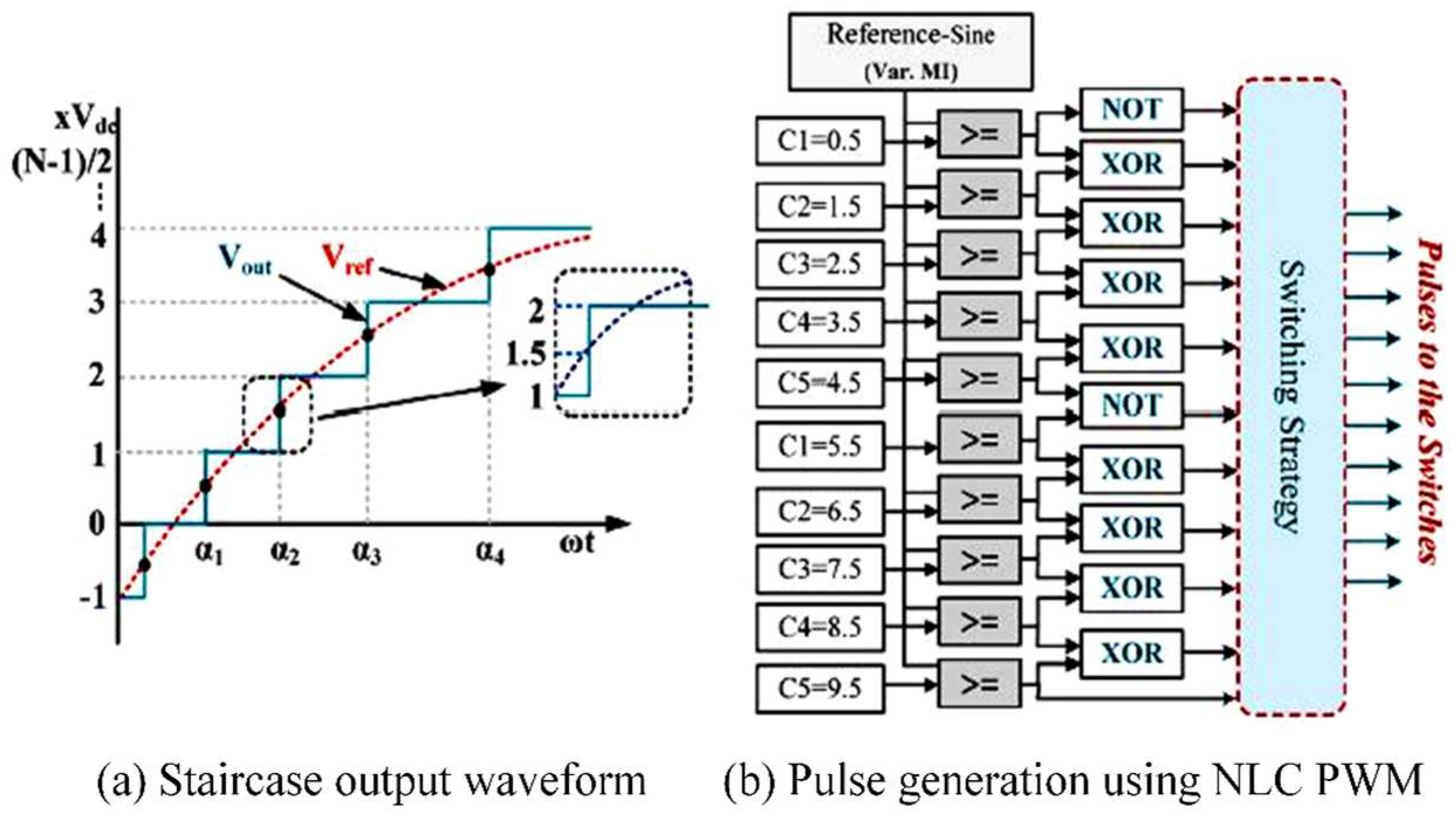
To generate the staircase output waveform, switches require pulses, which are generated using the pulse width modulation (PWM) technique. The proposed topology employs a low-frequency Nearest Level Control (NLC) PWM technique to implement switching operations [25]. Figure 3 shows the NLC PWM technique. The technique compares the reference waveform (a sine wave with a frequency of 50 Hz) with constant signals to get the appropriate voltage levels at the output. The switching state is changed using the switching logic given in Table 2. The reference waveform magnitude is determined by 0 ≤ Vm ≤ (NLevel − 1)/2 as described in Equation (1). The proposed topology is not limited by modulation techniques, and other techniques can be effectively applied to the converter, ensuring minimal switching losses.
V Ref = 10   sin   ( 2 π × 50   t )

2.5. Total Standing Voltage (TSV)

Total standing voltage (TSV) is a crucial factor in determining the feasibility of a topology and the appropriate switch ratings. The cost of switches and driver circuits primarily determines the cost of an MLI. The converter with a high value of TSV requires expensive switches, whereas low TSV allows the use of lower-rated switches, which makes the system more economical. The highest voltage across switches during the blocking state is added up mathematically to determine the TSV of MLI, which is calculated using the following relation [26]:
T S V = i = 1 k V m a x ( S i )
where S i is the i-th switch and V m a x ( S i ) is the highest voltage across the i-th switch. Figure 4 shows the voltage stress distribution across the switches. For the proposed topology, switches S2, S5, S9, and S10 must endure the highest stress of 10 V, and S1 and S4 experience the least stress of 4 V.
TSV = ( 2   ×   4   V DC ) + ( 4   ×   6   V DC ) + ( 4   ×   10   V DC )   =   72   V DC
To calculate the per-unit TSV, divide the absolute value of TSV by the peak value of output voltage. The per-unit TSV may be computed as:
TSVpu = T S V V o , m a x   =   7.2

2.6. Cost Analysis

The cost factor (CF) provides the economic feasibility of the converter. A topology with a high-cost factor indicates less feasibility. It depends on the number of IGBT, driver circuits, capacitors, diodes, TSV, and total DC sources. Since there are no capacitors or diodes in the proposed topology, the cost factor can be evaluated as:
CF = NDC + NIGBT + NGD + ND + NCap + TSVpu
CF = 4 + 14 + 10 + 0 + 0 + 7.2 = 35.2
CF/Level = 35.2/21 = 1.67

3. Results and Discussion

3.1. Simulation Results

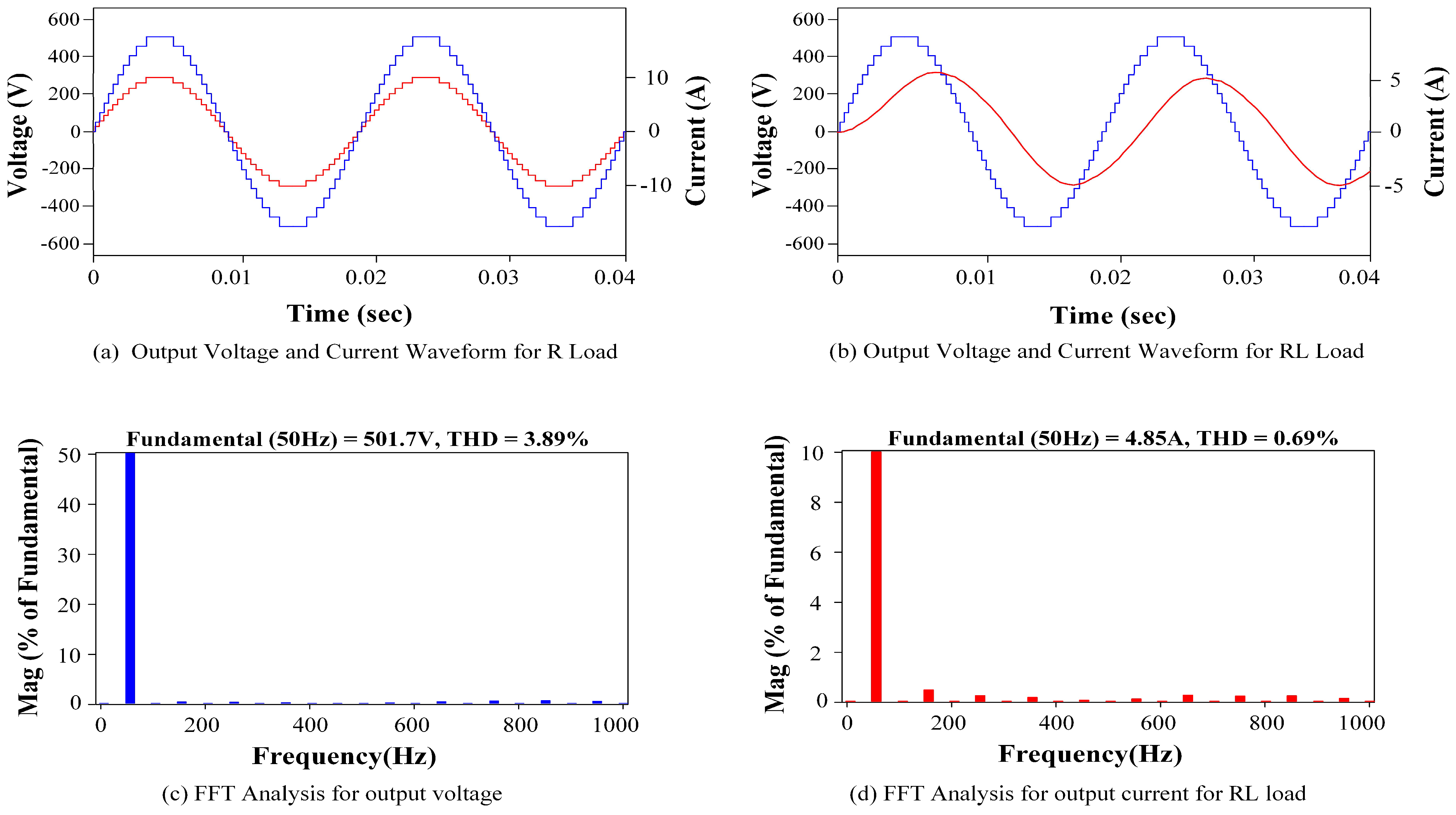
The performance of the proposed topology is studied using MATLAB/Simulink in an asymmetrical mode of operation. The static performance is tested for constant R and RL load, while its dynamic performance is tested for varying R, RL, load power factor, and modulation index. The simulation parameters are listed in Table 3.
The simulation results for constant loads are shown in Figure 5. For a purely resistive load of 50 Ω, the output voltage and current waveform are shown in Figure 5a. The converter achieves a maximum output voltage of 500 V and a load current of 10 A. For an RL load of 100 Ω + 40 mH, shown in Figure 5b, the output voltage generates 21 levels with a peak value of 500 V and a sinusoidal load current with a peak value of 5 A. Figure 5c depicts the FFT analysis of output voltage for constant load conditions. The output voltage offers a 3.89% THD with a fundamental value of 501.7 V. Figure 5d shows the harmonic profile of output current for RL load. The load current offers a 0.69% THD with a fundamental value of 4.85 A. It can be seen that all the harmonics are below 5%, which satisfies the IEEE-519 standard.
The dynamic performance of the proposed topology is also assessed to make sure it can tolerate sudden variations in load. As seen in Figure 6a, the converter was tested with a varying R load from 100 Ω to 50 Ω. The output voltage remains constant at 21 levels while the load current increases from 5 A to 10 A as the load changes, and the current waveform transitions are smooth without disturbance or transient. When the RL load is changed from 100 Ω + 80 mH to 50 Ω + 40 mH, the current increases with the load current being more sinusoidal due to the inductive effect shown in Figure 6b. The output voltage waveform remains constant and shows all desired voltage levels, indicating proper circuit operation.
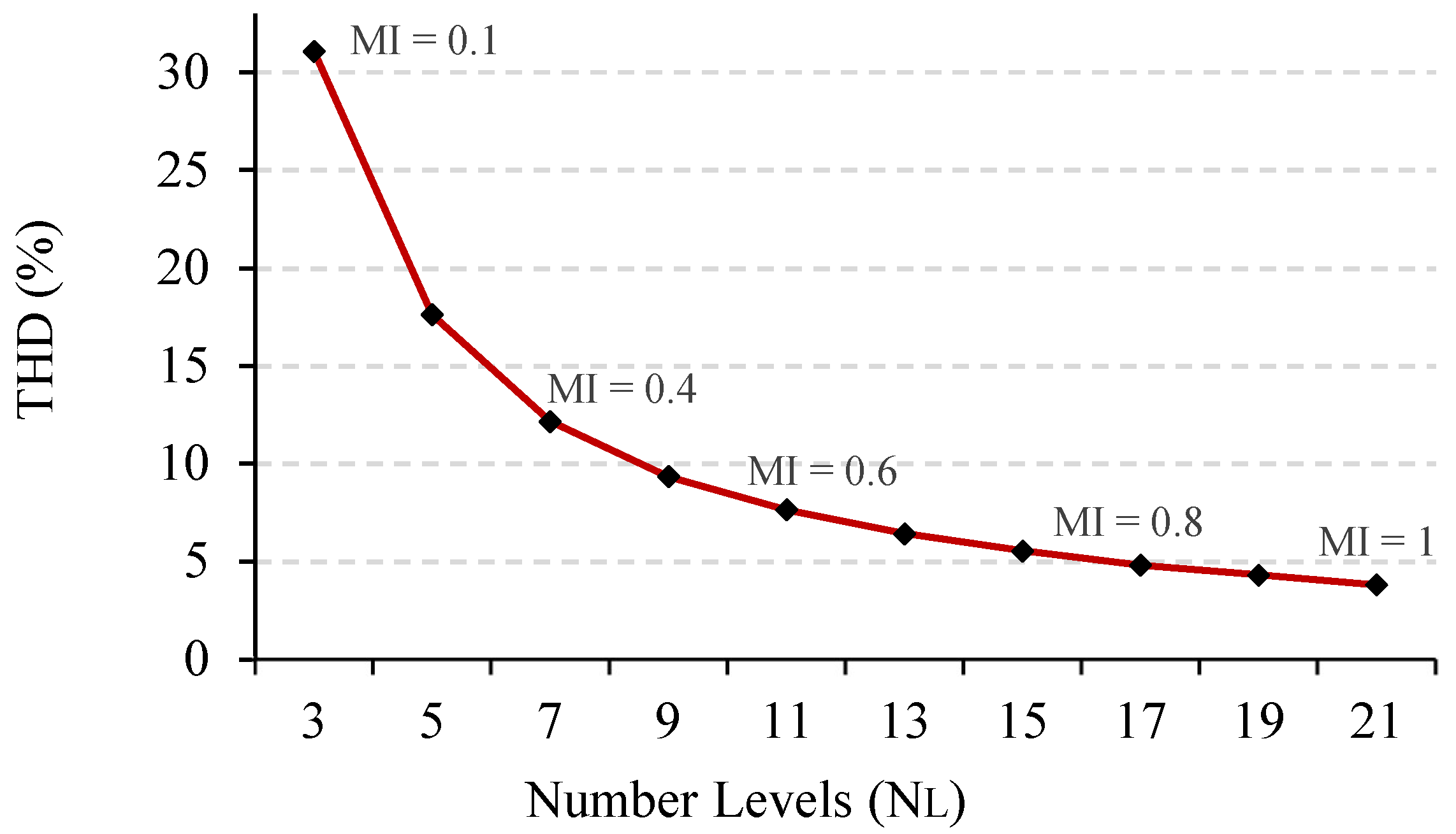
When the power factor changes from unity to a lagging power factor, as seen in Figure 6c, the output current changes from stepped to sinusoidal waveform due to load inductance, while the output voltage remains constant. The topology is also tested for varying Modulation Index (MI) from 1 to 0.6 and then to 0.4, as shown in Figure 6d. The results indicate that some voltage levels were not generated when the modulation index decreased from 1 to 0.4, and the output voltage levels dropped from 21 to 9. The modulation index also affects the THD. As the modulation index decreases, the output voltage may not closely resemble a sine wave, which increases the presence of higher-order harmonics, resulting in increased THD. Figure 7 shows the effects of change in modulation. The simulation results show that the proposed topology effectively performs under both fixed and variable load conditions.

3.2. Experimental Results

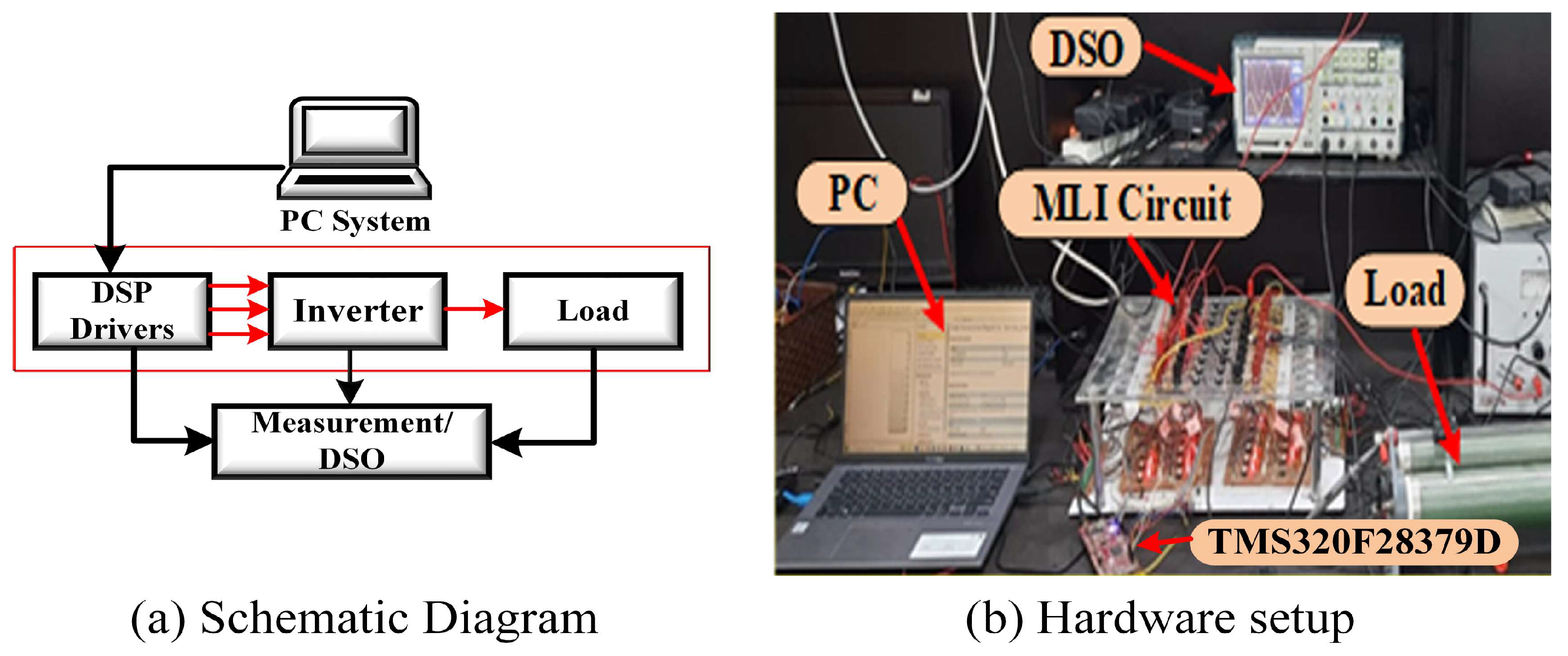
The real-time performance of the proposed topology is validated through laboratory testing. The hardware prototype is developed, as shown in Figure 8. The circuit uses IGBT FGA25N120 as a switch and a DSP board TMS320F28379D for PWM control signals. A driver circuit uses a TLP 250 optocoupler IC to drive the IGBTs. The circuit’s experimental testing involves four DC sources in the ratio of V1:V2:V3:V4 = 1:3:2:4, voltage and current waveforms recorded using a Yokogawa DL 1640 digital oscilloscope. A power quality analyzer, Fluke 435-II, is used to observe the harmonics content in the output. Table 4 provides information on the parameters and equipment used for hardware testing.
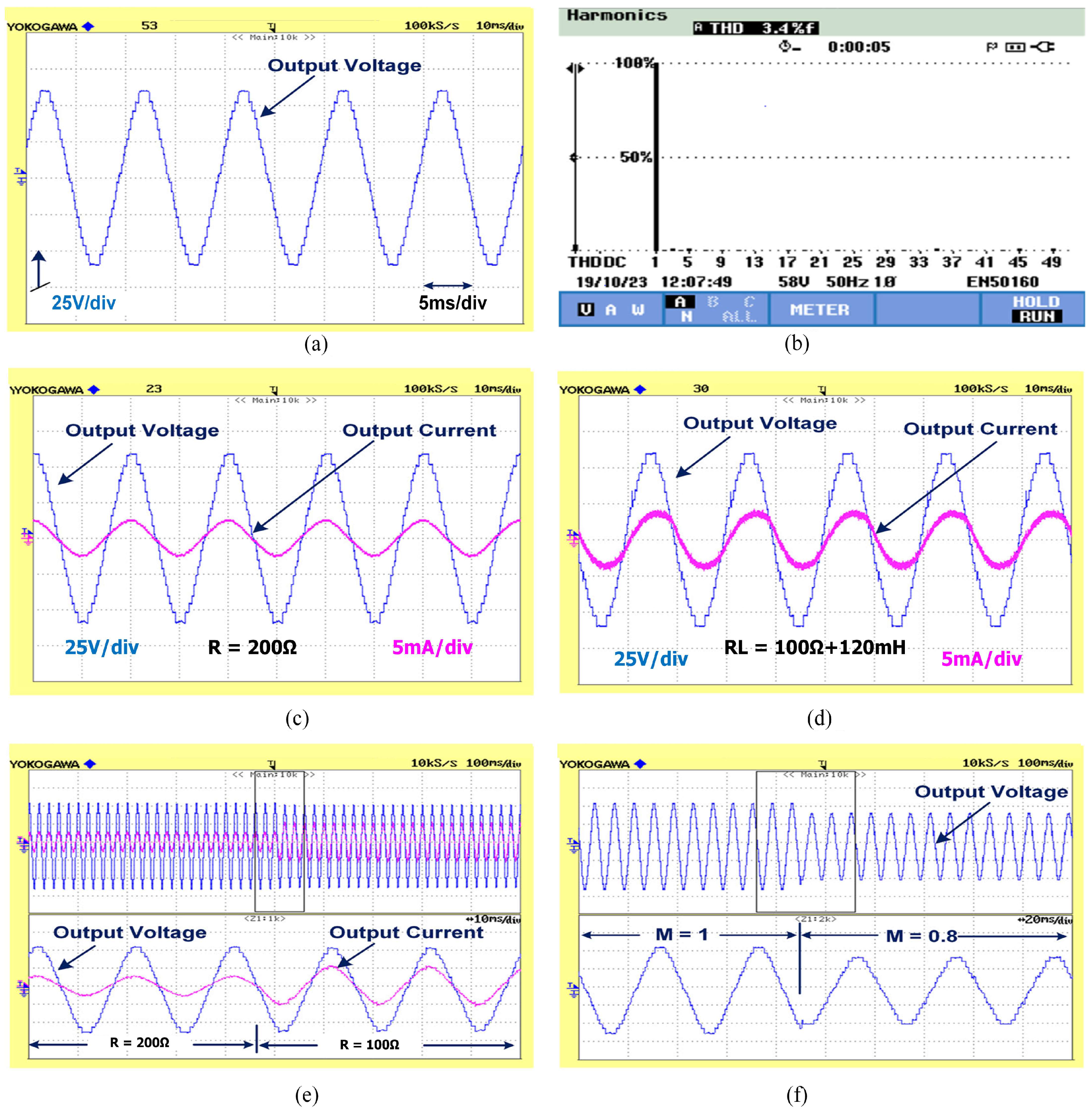
The hardware results for constant and dynamic loading conditions are presented in Figure 9. The 21-level output voltage for a constant R load of 200 Ω with a peak value of 60 V is shown in Figure 9a. The THD in output voltage is found to be 3.4%, as shown in Figure 9b. Figure 9c,d show the waveforms obtained at constant loading conditions. The R-load was set at 200 Ω, and the RL load was set at 100 Ω + 120 mH. The nature of the output current is sinusoidal for RL load, and the output voltage remains constant with a peak value of 60 V. The hardware result for dynamic loading conditions, depicted in Figure 9e, demonstrates the change in load from 200 Ω to 100 Ω. The load current smoothly increases while the output voltage remains constant. The effect of variation in the modulation index is depicted in Figure 9f. The modulation index was changed from 1 to 0.8, and the resulting waveform showed reduced voltage levels as the modulation index decreased. The results align with the simulation analysis, proving that the proposed topology performs satisfactorily in all conditions. The modulation index was changed from 1 to 0.8, and the resulting waveform showed reduced voltage levels as the modulation index decreased. The hardware results support the simulation analysis, demonstrating the satisfactory performance of the proposed topology under all loading conditions.

4. Power Loss Analysis

Power loss analysis is crucial for the power converter design as it affects the performance. The main losses in the proposed circuit are the conduction loss (PC) and switching loss (PS). Conduction losses are more effective at low frequencies, while switching losses dominate at high frequencies. The conduction losses that occur during the conduction time of the switches can be calculated as [27];
P C S = V s i ( t ) + R s i β ( t )
P C d = V d i ( t ) + R d i 2 ( t )
VS and Vd indicate the On-state voltage drop and RS and Rd represent the equivalent resistance of the switch and its antiparallel diode. The datasheet provides information on the value of constant β, which is affected by many factors. The total conduction loss of a switch is computed as:
P C = P s c + P c d
The average conduction loss of a converter is determined by the number of switches (NS) and diodes (Nd) conducting at an instant ‘t’, which can be calculated as:
P C = 1 π 0 π [ N s t { V s i t + R s i β t } + N d t { V d i t + R d i 2 t } ] d t
The energy loss is caused by turning ON and OFF, and the non-ideal operation of switches produces switching loss. The technique of nearest level modulation is implemented in this work to minimize switching frequency, hence lowering switching losses. The switching loss of semiconductors is affected by the voltage across the switch (Vsw), current flow through it (Isw), switching frequency (f), turn ON (Ton), and turn OFF (Toff) time of the switch [28,29]. The switching loss Ps is evaluated as:
P s = 1 6 f V s w I s w ( T o n + T o f f )
The proposed circuit’s total power loss can be expressed as:
P T = P c + P s
The efficiency is calculated as:
η = P o u t P o u t + P T × 100 %
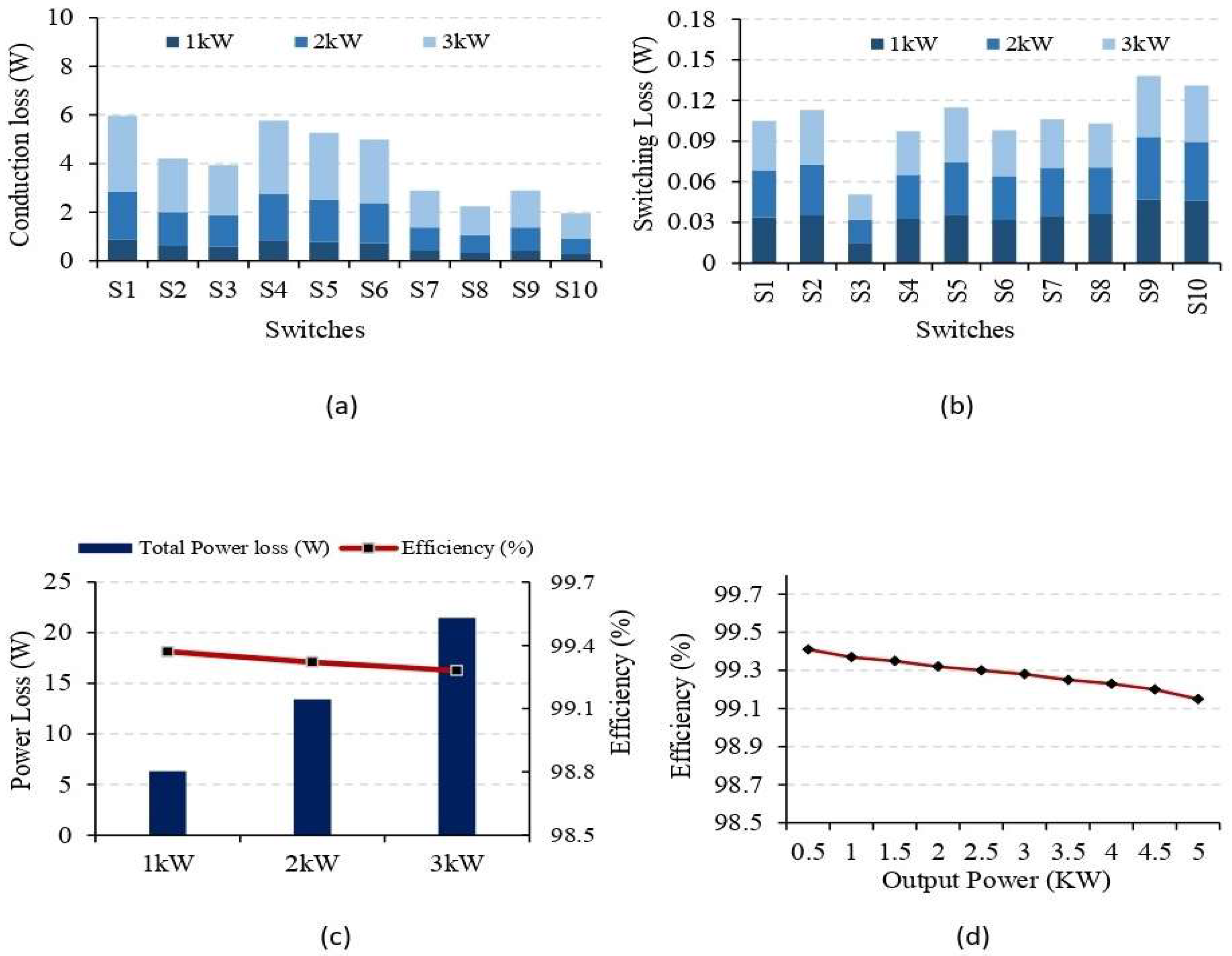
The proposed circuit’s efficiency and power loss are calculated using PLECS software. The IGBT datasheet is utilized for the PLECS lookup table data with real loss statistics, while the IGBT IKW40N65ES5 is used for thermal analysis and loss computation. As can be seen in Figure 10a and b, respectively, the study computes conduction and switching loss at different loads (1 KW. 2 KW, 3 KW). Switching losses occur when voltage and current take a longer time to drop to zero during turns ON and OFF—higher switching frequency resulting in more loss. The proposed converter’s low switching losses are attributed to its use of the low-frequency NLC PWM. Figure 10c depicts the variation of efficiency with total power losses. The efficiency of a converter is affected by total power losses, with higher power leading to increased conduction current and conduction losses, resulting in a decline in the converter efficiency. The proposed topology efficiency curve at different loads is shown in Figure 10d.

5. Comparative Analysis

This section compares the proposed topology with other similar asymmetrical multi-input multilevel inverter topologies available in the literature. The analysis considers parameters such as the number of output voltage levels (NL), number of DC sources (NDC), number of switches (NSW), number of IGBTs (NIGBT), gate driver circuits (NGD), number of capacitors (Ncap), number of diodes (Nd), switch per level (Nsw/NL), and cost factor per level (CF/Level). Table 5 summarizes the comparative analysis data and reveals that the proposed topology generates 21 levels of output voltage utilizing less device count and outperforms other MLIs due to its minimal value in the NSW/NL ratio and cost factor per level among all discussed topologies.
The topologies in [30,31,32,33,34] generate lower output voltage levels utilizing the same number of DC sources with a high switch per level ratio and cost factor per level. The topology in [31] required 12 IGBTs and 11 gate driver circuits for 15 levels of output, while the topology in [32] required 16 IGBTs and 14 gate driver circuits for 17 levels. The device count of these topologies is relatively high for less voltage-level topologies. If these topologies are cascaded for higher voltage levels, the device count increases significantly, affecting the inverter’s cost. Another 17-level topology with four DC sources utilizing less device count is proposed in [33], but the cost factor per level of the topology is high. The 19-level topology proposed in [16] required three DC sources, 13 IGBTs, and 13 gate drive circuits. The device count of the topology is very high and also has a high value of switch per level and cost factor. Another topology in [34] generates 19-level output voltage utilizing 4 DC sources and three capacitors. Due to the capacitors, the voltage balancing problem occurs, and the cost per level of the topology is high. The topology in [35] required six DC sources, 10 IGBTs, and three capacitors for 21 levels. However, the cost factor per level is higher than the proposed topology, making it less feasible. The topology in [36] required the same number of DC sources as the proposed topology for generating 21-level output voltage. However, they utilize a large device count with a high switch-per-level ratio and cost factor. Another 21-level topology with the same cost per level and switch per level ratio is proposed in [27]. However, the device count of the topology is higher than the proposed topology. From the above discussion, the proposed topology is suitable for medium and high voltage applications as it requires the least device count, a good switch per level ratio, and a cost factor for generating higher voltage levels. It outperforms other parameters and has less control complexity, demonstrating superior performance, economic viability, and increased stability despite potential outperformance in certain departments.

6. Application of the Proposed Topology

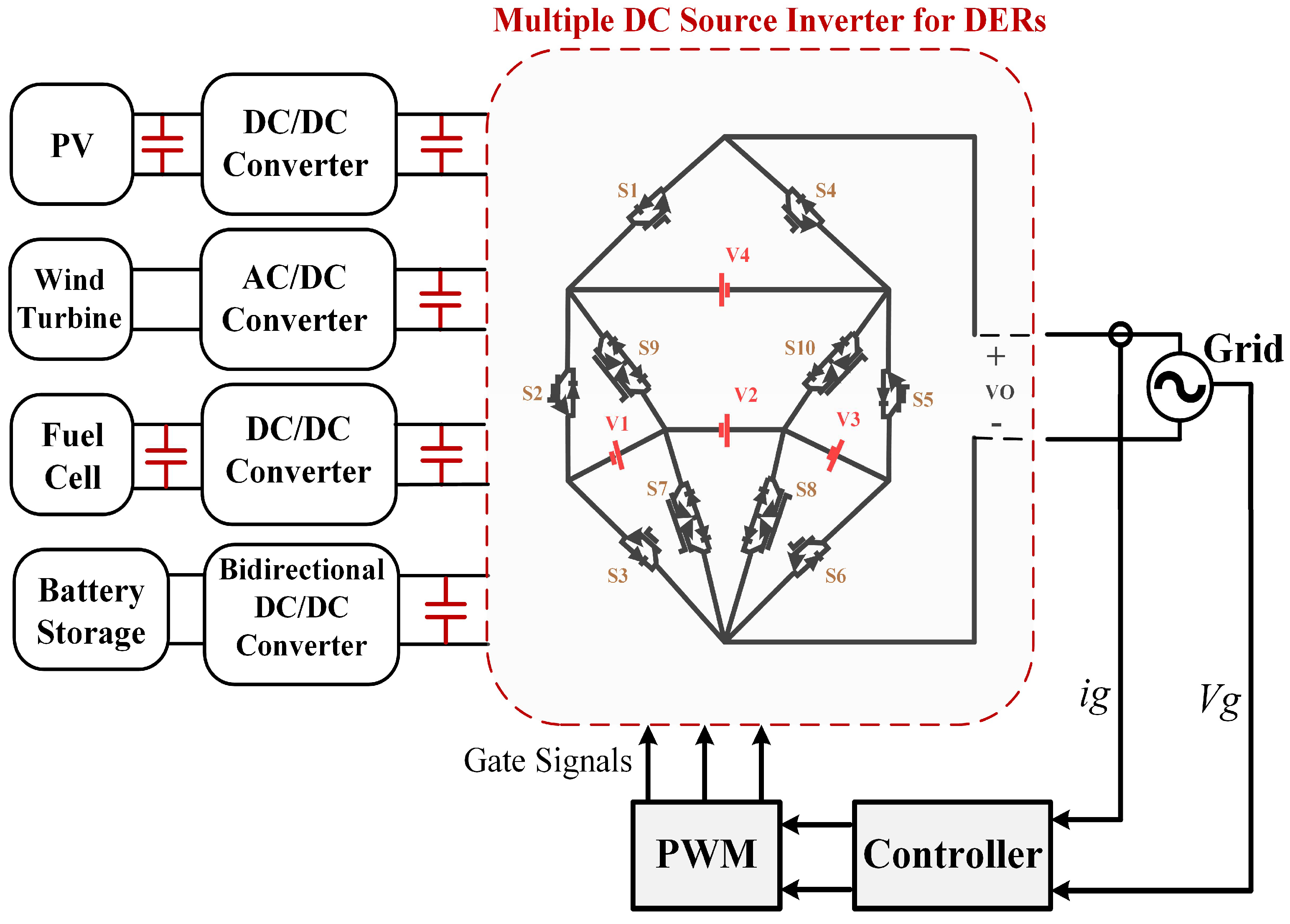
Distributed Energy Resources (DERs) [37,38,39], also referred to as DERs, are small-scale power generation and storage devices, including solar photovoltaic systems, hydroelectric generators, fuel cells, micro-turbines, wind turbines, and energy storage systems. Integrating DERs into the power grid is crucial due to the growing demand for renewable energy, improved grid resilience, and reduced greenhouse gas emissions [40,41,42]. Multilevel inverters convert DC power from renewable sources or energy storage systems [43] into AC power that is compatible with the grid. Unlike traditional two-level inverters, multiple DC source multilevel inverters use multiple voltage levels to synthesize an AC waveform, resulting in reduced harmonic distortion and improved efficiency. However, connecting multiple sources to a multi-input multilevel inverter (MIMLI) presents some challenges. The main challenge is to synchronize the incoming power, as sources may have variable voltage levels, which can cause distorted output waveforms, stress on the inverter, and uneven power distribution. To address the issues, DC–DC converter interfaces are required at each input source to maintain the desired voltage and current, and advanced control algorithms are designed to maintain complex power distribution and desired output voltage profile. The schematic diagram of the proposed multiple DC source inverter topology fed with different distributed resources is shown in Figure 11. Furthermore, the proposed topology can be used in electric vehicles [44,45,46].

7. Conclusions

This work presents a multi-input multilevel inverter topology (MIMLI) for distributed energy resources suitable for both symmetric and asymmetric configurations. The asymmetric configuration offers 21 output levels, requiring four DC sources in a 1:3:2:4 ratio, and 10 switches. The topology is evaluated in MATLAB under both static and dynamic loading conditions in an asymmetrical mode of operation using the low-frequency PWM technique. The proposed topology achieves less than 5% THD in output voltage and current, making it suitable for grid-tried applications. The conduction and switching losses are calculated using PLECS software, and an efficiency curve is presented to demonstrate implementation feasibility. Comparative analysis is conducted using recent literature to validate the proposed topology regarding device count for inverter design. The proposed circuit demonstrates its ability to generate desired voltage levels with fewer components and validate proper functioning through simulation and experimental results.

Author Contributions

Conceptualization, M.F.A., U.M. and M.S.B.A.; methodology, M.F.A. and U.M.; software, M.F.A.; validation, M.F.A., U.M. and M.S.B.A.; writing—original draft preparation, M.F.A. and M.A.; writing—review and editing, M.F.A., M.S.B.A. and M.A.; visualization, M.S.B.A.; supervision, J.R. and S.M.A. All authors have read and agreed to the published version of the manuscript.

Funding

Supported by ANID through projects FB0008, 1210208 and 1221293.

Data Availability Statement

Data are available on request from the authors.

Acknowledgments

J. Rodriguez acknowledges the support of ANID through projects FB0008, 1210208 and 1221293.

Conflicts of Interest

The authors declare no conflicts of interest.

References

  1. Memon, A.J.; Mahar, M.A.; Larik, A.S.; Shaikh, M.M. A Comprehensive Review of Reduced Device Count Multilevel Inverters for PV Systems. Energies 2023, 16, 5638. [Google Scholar] [CrossRef]
  2. Paul, S.; Jana, K.C.; Majumdar, S.; Pal, P.K.; Mahato, B. Performance analysis of a multimodule staircase (MM-STC)-type multilevel inverter with reduced component count and improved efficiency. IEEE J. Emerg. Sel. Top. Power Electron. 2021, 10, 6619–6633. [Google Scholar] [CrossRef]
  3. IEEE 519; IEEE Standards of Harmonic Control in Electric Power Systems. IEEE: Piscataway, NJ, USA, 2022.
  4. Huang, Z.; Zhou, D.; Wang, L.; Shen, Z.; Li, Y. A Review of Single-Stage Multiport Inverters for Multisource Applications. IEEE Trans. Power Electron. 2023, 38, 6566–6584. [Google Scholar] [CrossRef]
  5. Barzegarkhoo, R.; Forouzesh, M.; Lee, S.S.; Blaabjerg, F.; Siwakoti, Y. Switched-capacitor multilevel inverters: A comprehensive review. IEEE Trans. Power Electron. 2022, 37, 11209–11243. [Google Scholar] [CrossRef]
  6. Salem, A.; Van Khang, H.; Robbersmyr, K.G.; Norambuena, M.; Rodriguez, J. Voltage source multilevel inverters with reduced device count: Topological review and novel comparative factors. IEEE Trans. Power Electron. 2020, 36, 2720–2747. [Google Scholar] [CrossRef]
  7. Venkataramanaiah, J.; Suresh, Y.; Panda, A.K. A review on symmetric, asymmetric, hybrid and single DC sources based multilevel inverter topologies. Renew. Sustain. Energy Rev. 2017, 76, 788–812. [Google Scholar] [CrossRef]
  8. Omer, P.; Kumar, J.; Surjan, B.S. A review on reduced switch count multilevel inverter topologies. IEEE Access 2020, 8, 22281–22302. [Google Scholar] [CrossRef]
  9. Avanaki, H.N.; Barzegarkhoo, R.; Zamiri, E.; Yang, Y.; Blaabjerg, F. Reduced switch-count structure for symmetric multilevel inverters with a novel switched-DC-source submodule. IET Power Electron. 2018, 12, 311–321. [Google Scholar] [CrossRef]
  10. Vijeh, M.; Rezanejad, M.; Samadaei, E.; Bertilsson, K. A general review of multilevel inverters based on main submodules: Structural point of view. IEEE Trans. Power Electron. 2019, 34, 9479–9502. [Google Scholar] [CrossRef]
  11. Yousofi-Darmian, S.; Barakati, S.M. A new asymmetric multilevel inverter with a reduced number of components. IEEE J. Emerg. Sel. Top. Power Electron. 2019, 8, 4333–4342. [Google Scholar] [CrossRef]
  12. Yang, K.; Lan, X.; Zhang, Q.; Tang, X. Unified selective harmonic elimination for cascaded h-bridge asymmetric multilevel inverter. IEEE J. Emerg. Sel. Top. Power Electron. 2018, 6, 2138–2146. [Google Scholar] [CrossRef]
  13. Taghvaie, A.; Adabi, J.; Rezanejad, M. A multilevel inverter structure based on a combination of switched-capacitors and DC sources. IEEE Trans. Ind. Inform. 2017, 13, 2162–2171. [Google Scholar] [CrossRef]
  14. Hosseinzadeh, M.A.; Sarebanzadeh, M.; Rivera, M.; Babaei, E.; Wheeler, P. A Reduced Single-Phase Switched-Diode Cascaded Multilevel Inverter. IEEE J. Emerg. Sel. Top. Power Electron. 2020, 9, 3556–3569. [Google Scholar] [CrossRef]
  15. Kakar, S.; Ayob, S.B.M.; Iqbal, A.; Nordin, N.M.; Arif, M.S.B.; Gore, S. New Asymmetrical Modular Multilevel Inverter Topology With Reduced Number of Switches. IEEE Access 2021, 9, 27627–27637. [Google Scholar] [CrossRef]
  16. Dhanamjayulu, C.; Kaliannan, P.; Padmanaban, S.; Maroti, P.K.; Holm-Nielsen, J.B. A new three-phase multilevel asymmetrical inverter with optimum hardware components. IEEE Access 2020, 8, 212515–212528. [Google Scholar] [CrossRef]
  17. Shalchi Alishah, R.; Bertilsson, K.; Hosseini, S.H.; Babaei, E.; Aalami, M.; Ali, J.S.M.; Gharehpetian, G.B. A new generalized cascade multilevel converter topology and its improved modulation technique. Int. J. Circuit Theory Appl. 2021, 49, 1103–1120. [Google Scholar] [CrossRef]
  18. Majumdar, S.; Mahato, B.; Jana, K.C. Optimum structure-based multilevel inverter with doubling circuit configuration. J. Circ. Syst. Comput. 2019, 28, 1950194. [Google Scholar] [CrossRef]
  19. Rawa, M.; Mohamed Ali, J.S.; Siddique, M.D.; Mekhilef, S.; Wahyudie, A.; Seyedmahmoudian, M.; Stojcevski, A. A new multilevel inverter topology with reduced dc sources. Energies 2021, 14, 4709. [Google Scholar] [CrossRef]
  20. Mahato, B.; Majumdar, S.; Jana, K.C. Reduction in controlled power switches for a single-phase novel multilevel inverter. Int. J. Electron. 2019, 106, 1200–1215. [Google Scholar] [CrossRef]
  21. Mahato, B.; Majumdar, S.; Jana, K.C. A new and generalized MLI with overall lesser power electronic devices. J. Circ. Syst. Comput. 2020, 29, 2050058. [Google Scholar] [CrossRef]
  22. Akbari, A.; Ebrahimi, J.; Jafarian, Y.; Bakhshai, A. A Multilevel Inverter Topology with an Improved Reliability and a Reduced Number of Components. IEEE J. Emerg. Sel. Top. Power Electron. 2022, 10, 553–563. [Google Scholar] [CrossRef]
  23. Maamar, A.E.T.; Kermadi, M.; Helaimi, M.; Taleb, R.; Mekhilef, S. An Improved Single-Phase Asymmetrical Multilevel Inverter Structure with Reduced Number of Switches and Higher Power Quality. IEEE Trans. Circuits Syst. II Express Briefs 2021, 68, 2092–2096. [Google Scholar] [CrossRef]
  24. Oskuee, M.R.J.; Karimi, M.; Naderi, Y.; Ravadanegh, S.N.; Hosseini, S.H. A new multilevel voltage source inverter configuration with minimum number of circuit elements. J. Cent. South. Univ. 2017, 24, 912–920. [Google Scholar] [CrossRef]
  25. Deliri, S.; Varesi, K.; Padmanaban, S. An extendable single-input reduced-switch 11-level switched-capacitor inverter with quintuple boosting factor. IET Gener. Transm. Distrib. 2023, 17, 621–631. [Google Scholar] [CrossRef]
  26. Karakılıç, M.; Hata¸s, H.; Nuri Almalı, M. Design of a 21-level multilevel inverter with minimum number of devices count. Int. J. Circ. Theor. Appl. 2023, 51, 5705–5723. [Google Scholar] [CrossRef]
  27. Arif, M.S.B.; Mustafa, U.; Ahmad, S.; Ayob, S.B.; Ashique, R.H.; Tayyab, M. Asymmetrical 21-level inverter topology with minimum variety of dc sources and reduced component counts. Int. J. Circ. Theor. Appl. 2023, 51, 1697–1718. [Google Scholar] [CrossRef]
  28. Karimi, M.; Kargar, P.; Varesi, K. An extendable asymmetric boost multilevel inverter with self-balanced capacitors. Int. J. Circ. Theor. Appl. 2022, 50, 1297–1316. [Google Scholar] [CrossRef]
  29. Deliri Saeid Varesi, K.; Siwakoti, Y.P.; Blaabjerg, F. Generalized diamond-type single DC-source switched-capacitor based multilevel inverter with step-up and natural voltage balancing capabilities. IET Power Electron. 2021, 14, 1208–1218. [Google Scholar] [CrossRef]
  30. Arif, M.S.B.; Sarwer, Z.; Siddique, M.D.; Ayob, S.; Iqbal, A.; Mekhilef, S. Asymmetrical multilevel inverter topology with low total standing voltage and reduced switches count. Int. J. Circuit Theory Appl. 2021, 49, 1757–1775. [Google Scholar] [CrossRef]
  31. Fahad, M.; Siddique, M.D.; Iqbal, A.; Sarwar, A.; Mekhilef, S. Implementation and analysis of a 15-level inverter topology with reduced switch count. IEEE Access 2021, 9, 40623–40634. [Google Scholar] [CrossRef]
  32. Dhanamjayulu, C.; Prasad, D.; Padmanaban, S.; Maroti, P.K.; Holm-Nielsen, J.B.; Blaabjerg, F. Design and implementation of seventeen level inverter with reduced components. IEEE Access 2021, 9, 16746–16760. [Google Scholar] [CrossRef]
  33. Samadaei, E.; Sheikholeslami, A.; Gholamian, S.A.; Adabi, J. A square T-type (ST-type) module for asymmetrical multilevel inverters. IEEE Trans. Power Electron. 2017, 33, 987–996. [Google Scholar] [CrossRef]
  34. Hassan, A.; Yang, X.; Chen, W. A novel 19L hybrid multilevel inverter system synthesizes reduced number of switches for hybrid renewable energy applications. Int. Trans. Electr. Energy Syst. 2021, 31, e12856. [Google Scholar] [CrossRef]
  35. Meraj, S.T.; Yahaya, N.Z.; Hasan, K.; Masaoud, A. Single phase 21 level hybrid multilevel inverter with reduced power components employing low-frequency modulation technique. Int. J. Power Electron. Drive Syst. 2020, 11, 810–822. [Google Scholar] [CrossRef]
  36. Agrawal, R.; Jain, S. Multilevel inverter for interfacing renewable energy sources with low/medium-and high-voltage grids. IET Renew. Power Gen. 2017, 11, 1822–1831. [Google Scholar] [CrossRef]
  37. Lu, Z.; Wang, J.; Shahidehpour, M.; Bai, L.; Xiao, Y.; Li, H. Cooperative Operation of Distributed Energy Resources and Thermal Power Plant with a Carbon-Capture-Utilization-and-Storage System. IEEE Trans. Power Syst. 2024, 39, 1850–1866. [Google Scholar] [CrossRef]
  38. Shirkhani, M.; Tavoosi, J.; Danyali, S.; Sarvenoee, A.K.; Abdali, A.; Mohammadzadeh, A.; Zhang, C. A review on microgrid decentralized energy/voltage control structures and methods. Energy Rep. 2023, 10, 368–380. [Google Scholar] [CrossRef]
  39. Duan, Y.; Zhao, Y.; Hu, J. An initialization-free distributed algorithm for dynamic economic dispatch problems in microgrid: Modeling, optimization and analysis. Sustain. Energy Grids Netw. 2023, 34, 101004. [Google Scholar] [CrossRef]
  40. Lin, X.; Wen, Y.; Yu, R.; Yu, J.; Wen, H. Improved Weak Grids Synchronization Unit for Passivity Enhancement of Grid-Connected Inverter. IEEE J. Emerg. Sel. Top. Power Electron. 2022, 10, 7084–7097. [Google Scholar] [CrossRef]
  41. Shao, B.; Xiao, Q.; Xiong, L.; Wang, L.; Yang, Y.; Chen, Z.; Blaabjerg, F.; Guerrero, J.M. Power coupling analysis and improved decoupling control for the VSC connected to a weak AC grid. Int. J. Electr. Power Energy Syst. 2023, 145, 108645. [Google Scholar] [CrossRef]
  42. Shen, Y.; Liu, D.; Liang, W.; Zhang, X. Current Reconstruction of Three-Phase Voltage Source Inverters Considering Current Ripple. IEEE Trans. Transp. Electrif. 2023, 9, 1416–1427. [Google Scholar] [CrossRef]
  43. Hu, J.; Zou, Y.; Soltanov, N. A multilevel optimization approach for daily scheduling of combined heat and power units with integrated electrical and thermal storage. Expert Syst. Appl. 2024, 250, 123729. [Google Scholar] [CrossRef]
  44. Hou, M.; Zhao, Y.; Ge, X. Optimal scheduling of the plug-in electric vehicles aggregator energy and regulation services based on grid to vehicle. Int. Trans. Electr. Energy Syst. 2017, 27, e2364. [Google Scholar] [CrossRef]
  45. Zhang, X.; Lu, Z.; Yuan, X.; Wang, Y.; Shen, X. L2-Gain Adaptive Robust Control for Hybrid Energy Storage System in Electric Vehicles. IEEE Trans. Power Electron. 2021, 36, 7319–7332. [Google Scholar] [CrossRef]
  46. Fang, Z.; Liang, J.; Tan, C.; Tian, Q.; Pi, D.; Yin, G. Enhancing Robust Driver Assistance Control in Distributed Drive Electric Vehicles through Integrated AFS and DYC Technology. IEEE Trans. Intell. Veh. 2024, 1–14. [Google Scholar] [CrossRef]
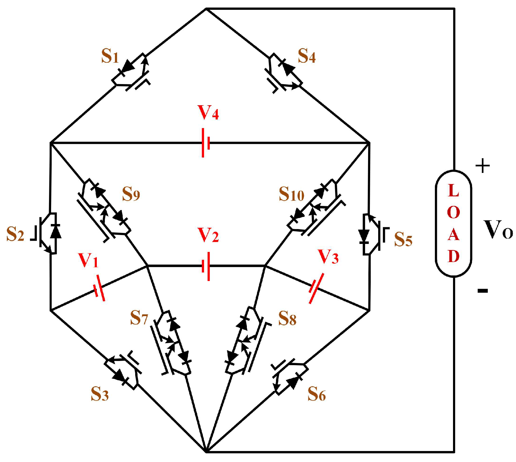
Figure 1. Circuit diagram of the proposed topology.
Energies 17 02146 g001
Figure 2. Current conduction path during the positive half-cycle.
Energies 17 02146 g002
Figure 3. NLC PWM modulation technique.
Energies 17 02146 g003
Figure 4. Voltage stress across each switch.
Energies 17 02146 g004
Figure 5. Simulation results under constant loading conditions (blue for voltage, red for current).
Energies 17 02146 g005
Figure 6. Simulation results under dynamic loading conditions.
Energies 17 02146 g006
Figure 7. Effect of change in Modulation Index (MI).
Energies 17 02146 g007
Figure 8. Experimental setup of the proposed MI-MLI Circuit.
Energies 17 02146 g008
Figure 9. Experimental results of the proposed topology under constant and dynamic loading conditions.
Energies 17 02146 g009
Figure 10. Power loss and efficiency curve under different loading conditions (a) Conduction losses (b) Switching Losses (c) Total Power Loss and Efficiency Curve and (d) Output Power v/s Efficiency Curve.
Energies 17 02146 g010
Figure 11. Schematic diagram of the proposed topology fed with different distributed resources.
Energies 17 02146 g011
Table 1. Selection of DC Source.
AlgorithmMagnitude of DC Voltage SourceOutput Voltage Levels,
(NL)
I V 1 = V 2 = V 3 = V 4 = N L 1 8 V 9
II V 1 = V 2 = V 3 = N L 1 10 V ,       V 4 = N L 1 5 V 11
III V 1 = V 3 = N L 3 10 V ,         V 2 = V 4 = N L 3 5 V 13
IV V 1 = N L 5 10 V ,         V 2 = V 3 = V 4 = N L 5 5 V 15
V V 1 = N L 7 10 V ,       V 2 = V 3 = N L 7 5 V ,     V 4 = N L 2 5 V 17
VI V 1 = N L 9 10 V ,     V 2 = V 4 = N L 4 5 V ,     V 3 = N L 9 5 V 19
VII V 1 = N L 11 10 V ,     V 2 = N L 11 5 V ,     V 3 = N L 6 5 V ,     V 4 = N L 1 5 V 21
Table 2. Switching States For 21-Level Asymmetrical Configuration.
VoS1S2S3S4S5S6S7S8S9S10VinPositive Levels
1 V1010000010V1
2 V0001100100V3
1000010001V4 − V3
3 V0001001001V2
4 V1000110000V4
0011000001V1 + V2
5 V0001101000V2 + V3
6 V0011100000V1 + V2 + V3
1000100100V3 + V4
7 V1000001001V2 + V4
8 V1010000001V1 + V2 + V4
9 V1000101000V2 + V3 + V4
10 V1010100000V1 + V2 + V3 + V4
01110000000Zero Level
0001110000
−1 V1100001000−V1Negative Levels
−2 V0001010001−V3
−3 V1000000110−V2
−4 V0001001010−V4
1100000100−V1 − V2
−5 V1000010010−V2 − V3
−6 V1100010000−V1 − V2 − V3
−7 V0001000110−V2 − V4
−8 V0101000100−V1 − V2 − V3
−9 V0001010010−V2 − V3 − V4
−10 V0101010000−V1 − V2 − V3 − V4
Table 3. Simulation parameters.
Parameter/DeviceValue
DC SourcesV1 = 50 V, V2 = 150 V, V3 = 100 V, V4 = 200 V
SwitchesIGBT
Load Resistance100 Ω, 50 Ω
Load Inductance80 mH, 40 mH
Modulation Index1, 0.6, 0.4
Table 4. Experimental parameters and equipment.
Parameter/DeviceValue/Type/Rating
DC SourcesV1 = 6 V, V2 = 18 V, V3 = 12 V, V4 = 24 V
SwitchesIGBT, FGA25N120, 1200 V/25 A
MicrocontrollerTMS320F28379D, 200 MHz
Driver ICTLP 250
Digital Signal OscilloscopeYokogawa DL1640
Power Quality AnalyzerFluke 435-II
Load Resistance100 Ω, 200 Ω
Load Inductance90 mH, 120 mH
Modulation Index1, 0.8
Table 5. Comparison with other asymmetrical Muti-Input Multilevel Inverter (MIMLI) topologies.
TopologyNLNDCNSWNIGBTNGDNCapNdNSW/NLCF/Level
[30]1548108000.531.78
[31]154111211000.732.14
[32]174141614200.821.97
[33]1749129000.531.76
[16]193131313000.681.69
[34]194101110320.531.79
[35]216101010300.481.57
[36]214121612400.671.88
[27]214121212020.481.53
Proposed214101410000.481.53
Disclaimer/Publisher’s Note: The statements, opinions and data contained in all publications are solely those of the individual author(s) and contributor(s) and not of MDPI and/or the editor(s). MDPI and/or the editor(s) disclaim responsibility for any injury to people or property resulting from any ideas, methods, instructions or products referred to in the content.