Article

Local DER Control with Reduced Loop Interactions in Active Distribution Networks

Department of Electrical and Information Engineering, University of Cassino and Southern Lazio, Via G. Di Biasio 43, 03043 Cassino, Italy
*
Author to whom correspondence should be addressed.
These authors contributed equally to this work.
Energies 2024, 17(9), 1991; https://doi.org/10.3390/en17091991
Submission received: 23 March 2024 / Revised: 12 April 2024 / Accepted: 19 April 2024 / Published: 23 April 2024

Abstract

:
Active Distribution Networks are Multi-Input Multi-Output (MIMO) systems with coupled dynamics, which cause interactions among the control loops of Distributed Energy Resources (DERs). This undesired effect leads to performance degradation of voltage control. To mitigate the effects of this unavoidable coupling, the present paper proposes a systematic design procedure based on the analysis of the interaction’s sources. In detail, each DER is equipped with a double-loop PI to control the active and reactive power output of the voltage source converter, which connects the DER to the network’s node. Furthermore, to guarantee ancillary services, the two loops are coupled by a simple mechanism of cooperation of the active power to voltage regulation realized by a filtered droop law. To achieve voltage regulation with reduced loop interactions, the PI parameters and the filter’s pulse are designed according to a procedure with two sequential steps based on the Internal Model Control (IMC) technique. Simulation studies are finally presented to demonstrate that the proposed design method achieves both reduction of the loop interaction and robust voltage control in the presence of model parameter uncertainty in the MIMO plant, modeling various operating conditions of the ADN, including a step connection of large loads, renewable energy source variations, and changes in the substation transformer ratio.

1. Introduction

In the last decade, electric distribution systems have undergone substantial changes to allow large penetration of Distributed Generation (DG) exploiting Renewable Energy Resources (RESs). Their configuration has changed from passive to Active Distribution Networks (ADNs), and new Distributed Energy Sources (DERs) are being connected, which include, in addition to DG, Battery Energy Storage Systems (BESSs), controllable loads, and Electric Vehicles (EVs).
A key issue in ADNs is the regulation of the voltage profiles, which are no longer monotonic along the feeders and can violate the quality limits of over and under voltage. In distribution systems, voltage regulation is traditionally poorly automated and essentially centralized. Then, the new ADNs require all the DERs to support the voltage regulation. In particular, it is possible to act on the inverters interfacing the DERs to grid so as to vary their reactive power injections with no impact on the operation of the DC bus of the DER and, consequently, on the RES generator. However, due to the high R / X ratio of distribution lines, the control of the reactive power injection is not effective enough to assure an adequate voltage regulation. Thus, Active Power Curtailment (APC) has been proposed as an additional tool for voltage regulation. In [1], the control system prioritizes the use of reactive power, while APC is performed only as a last resort; the controllers switch to active power curtailment only if all the reactive power capability has been exploited. In [2], a method that includes APC in coordination with reactive power control for voltage control in distribution networks is presented: APC is applied if the inverter rated apparent power is reached.
However, the approaches exploiting APC generally present two drawbacks. The first one is the non-linear behavior of the control systems, which often adopt a switching strategy between reactive power control and APC. To overcome this issue, the proposed voltage control methods typically use different control layers that are adequately coordinated to manage both reactive power and APC [3,4,5]. The second important drawback is the economical impact of APC: it wastes energy produced from RESs and reduces revenues [6]. To reduce the economic impact, some methods use voltage-active sensitivity factors to define the optimal APC strategy with respect to some chosen objectives, such as acting with priority on the most voltage-effective PV system [7] so as to limit the overall curtailment. To really overcome this problem, BESS should be installed to store excessive PV-produced energy during peak generation periods and then use it to supply active power for voltage regulation [8]. But the BESS equipment is usually expensive, making it difficult to be justified from the cost–benefit point of views [9].
Recently, the asset of distribution systems with DERs has significantly changed because of the environmental requirements that push towards the complete substitution of conventional energy sources with RESs. To allow a further increase in RESs in distribution systems, two main innovations are being introduced:
  • new ancillary services (ASs) provided by DERs at ADN level are being defined [10] and commercialized in deregulated markets [9];
  • new market agents are being introduced that aggregate DERs to provide ASs at transmission system level [11], in particular by mitigating the negative effects of RES power fluctuations [12], as well as new entities, such as energy communities [13], to promote the power balance and the AS provision at distribution system level.
Such innovations favor the installation of BESSs in conjunction with RES generators because ASs can provide additional incomes that justify the cost of BESSs. For this reason, the present paper focuses attention on DERs composed of DG-exploiting RESs equipped with BESS and interfaced to the ADN by a Voltage Source Converter (VSC). This type of DER is commonly equipped with a local controller that guarantees voltage regulation at a node of connection with the network.
As is well known, any local controller interacts with each other through the distribution lines of the ADN when they act on multiple DERs connected to the same feeder [14]. This mutual interaction leads to system operating conflicts and also to voltage instability [15,16,17]. The techniques employed to address this problem are categorized into two main approaches [18,19]. The first is based on centralized and/or distributed techniques, which guarantee optimal solutions to the voltage control problem, for example, in term of power loss minimization [20,21,22,23]. A general issue with the aforementioned techniques is that they are based on field network measurements in a closed loop real-time control system [24,25]. However, the implementation of a communication-based control strategy may not be practical in active distribution networks that lack information on infrastructures or the whole control scheme fails to work if a communication failure occurs [26]. The main drawback of the centralized solutions is the computational cost to handle the large amount of data measured by the ADN. On the contrary, distributed control algorithms require less information, coming from the neighboring DERs, with respect to centralized solutions but may suffer from a slow convergence rate [27]. The second approach relies on the use of decentralized techniques. Generally they do not give optimal solutions since they use only local information and measurements. However, as previously noted, due to the requirement of a large amount of information exchange and increased needed computing capacity, decentralized techniques are usually preferred since they can be implemented in the existing distribution networks easily. Furthermore, they are less complex and more reliable compared to centralized/distributed techniques [28].
Based on the previous considerations, the motivation for this paper is to present a possible solution to the voltage control problem in ADNs in the presence of strong mutual interactions among DERs and possible saturation of the reactive currents. Keeping the simplicity of a completely decentralized architecture, the scope of the paper is the development of the method proposed in this paper applicable to local control of DERs in order to regulate the voltage at node where the DER is connected. In detail, each local controller acts on the reactive power of the inverter and, if necessary, provides an additional AS by varying the active power injected by the DER. In particular, the AS is defined by its droop characteristic and by the range of power variation allowed by the BESS. Moreover, the local control scheme should both avoid the introduction of any switching mechanism between reactive and active power control and mitigate the interaction’s level.
To pursue this objective, in the proposed approach, each DER is equipped with two PI local control loops based on Internal Model Control (IMC), which regulate, respectively, the voltage and active power to the desired set points. Moreover, the two control loops are coupled by a filtered droop control law, which realizes the AS. Based on the Relative Gain Matrix (RGA) of the adopted Multi-Input Multi-Output (MIMO) system dynamically coupled to the ADN, a design method is proposed that is articulated in two sequential steps. In the first one, each PI-IMC voltage controller is designed for the corresponding Effective Open-Loop Transfer Function (EOTF) [29], where the free parameters of all controllers are designed to mitigate the interactions among the voltage control loops in a frequency range of interest (external interaction). In the second step, due to the reduced external interaction, the free parameters of all PI-IMC active-power controllers and the cut-off frequency of all filters are designed to mitigate the interaction between the voltage and active power control loop of any DER (internal interaction). The robust stability of the IMC-PI controllers is also investigated in the presence of model parameter uncertainty modeling unknown scenarios of the ADN.
In summary, the contributions of this paper can be synthesized as follows:
  • The AS of voltage regulation provided by DERs locally varying, primarily, their reactive power injection according to an integral law, and, in the case of reactive current saturation, their active power injection according to a given droop law.
  • A two-step-based sequential design using only local measurements.
  • Reduction in the internal and external interaction level.
  • Robust stability in the presence of parameter uncertainty in the matrix model plant.
  • Simplicity of the controller’s structure easily implementable in real ADNs.
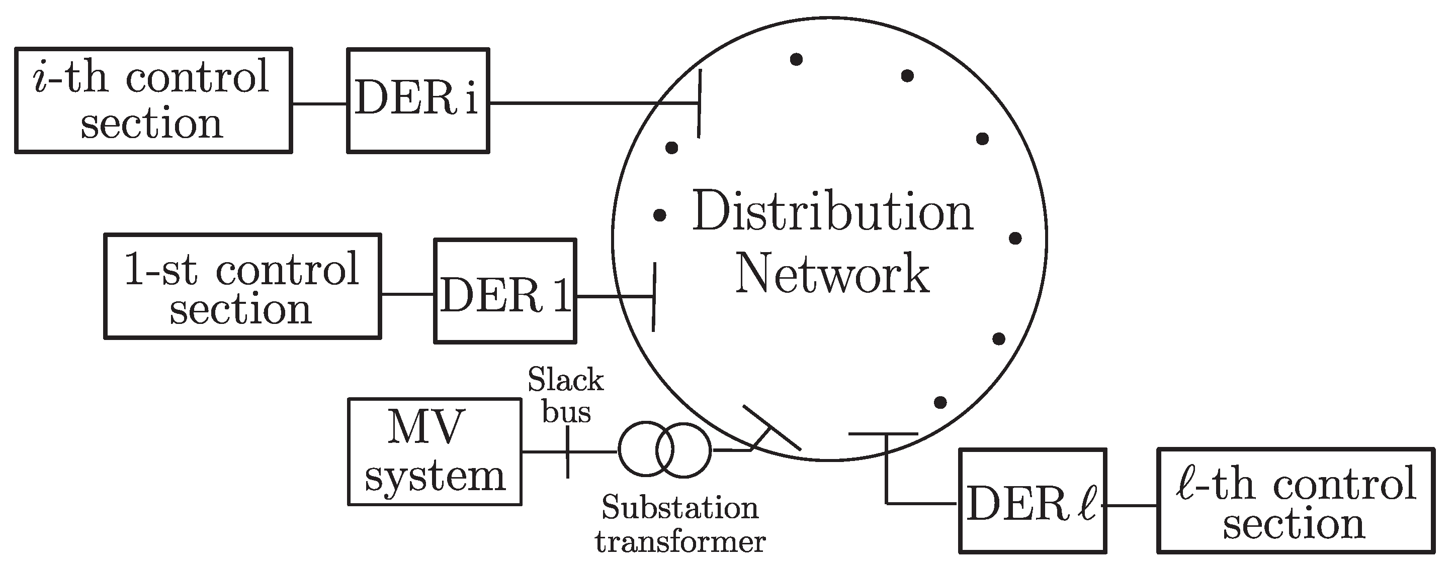
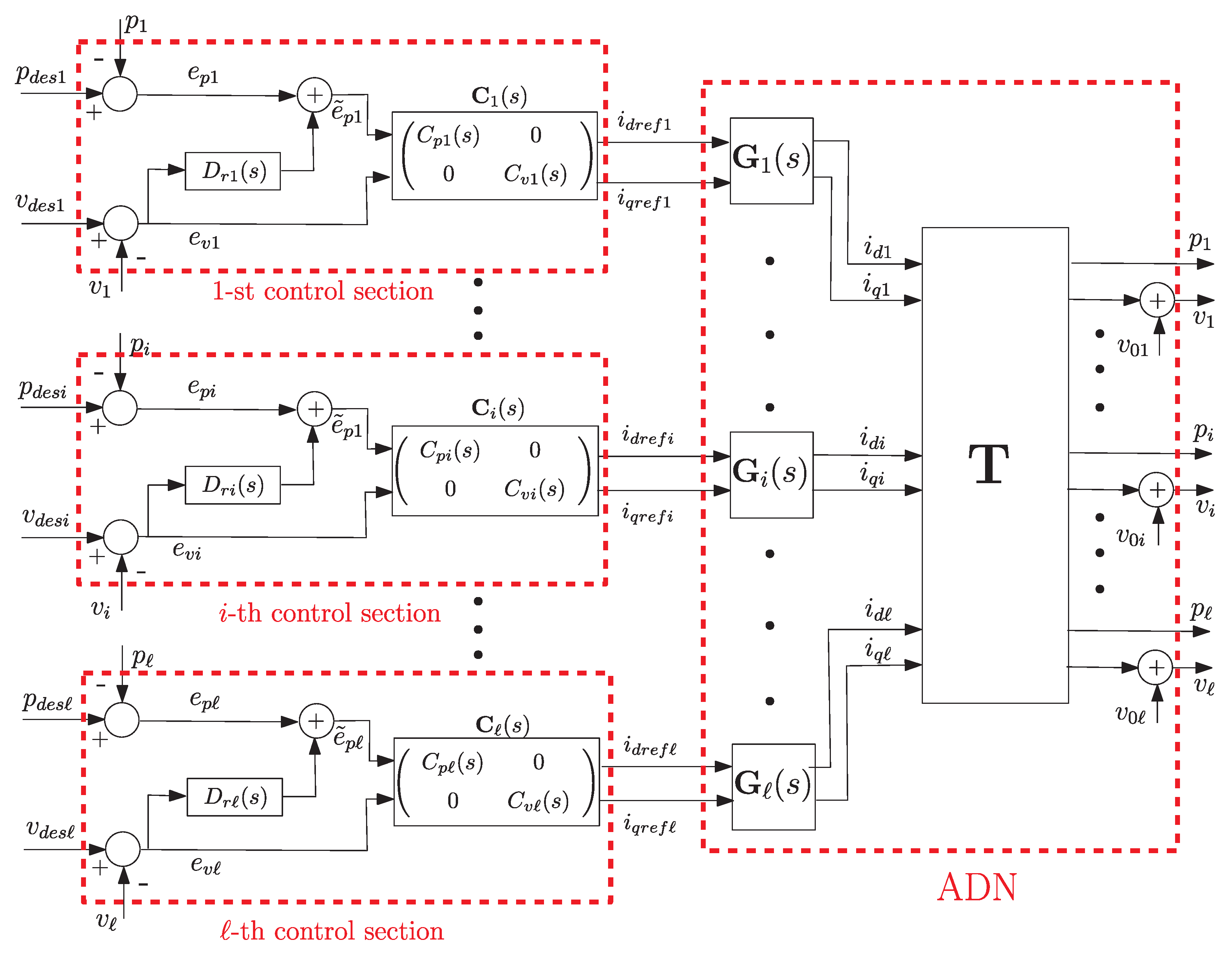
This paper is organized as follows. In Section 2, the adopted model of the ADN is firstly recalled; subsequently, the proposed technique is illustrated, and its robust stability is validated. Finally, Section 3 is devoted to the development of detailed numerical case studies based on simulations and aimed at validating the performance of our technique also in comparison with the technique proposed in [30].

2. ADN Model

The schematic representation of an ADN is reported in Figure 1 with reference to an LV distribution grid. The passive distribution network is composed of feeders, laterals, and passive loads, and it is supplied by an MV system (which is assumed to be the slack bus) and a substation MV/LV transformer. The -controlled DERs are connected to various nodes of the distribution grid.
The design of the DER control in Section 3 assumes the ADN model presented in [31], which is briefly recalled hereafter. The model is composed of the combination of the DER models and of the distribution grid model, which includes the passive distribution network, the supplying MV system, and the substation transformer.
Concerning the DERs, they are assumed to be composed of a renewable energy generator and a battery energy storage system, both connected on a DC bus, which is interfaced to the distribution grid by a VSC, an AC filter, and a transformer. According to [32], the following Two-Input Two-Output (TITO) model is adopted to represent the closed-loop transfer function of the current control loops of the VSC, acting on the d q components
i i d i i q T = G i ( s ) i d r e f i i d r e f i T
where the transfer function matrix G i ( s ) is expressed by
G i ( s ) = 1 1 + s τ i d k i 1 s ( 1 + s τ i 1 ) ( 1 + s τ i 2 ) k i 2 s ( 1 + s τ i 3 ) ( 1 + s τ i 4 ) 1 1 + s τ i q j = 1 ,
Concerning the distribution grid, it is modeled by the full 2 x 2 algebraic matrix T , which linearly represents the effect of the vector ( i d 1 , i q 1 , , i d , i q ) of the currents injected by the DERs on the output vector y = ( p 1 , v 1 , , p , v ) of the injected active powers and of the DER nodal voltages.
The resulting model of the ADN, including both the DERs and the distribution grid, is
y = y 0 + P ( s ) u with P ( s ) = T G ( s )
where P ( s ) is the MIMO model with 2 inputs u = ( i d r e f 1 , i q r e f 1 , , i d r e f , i q r e f ) and outputs y and G ( s ) = d i a g { G i ( s ) } . Moreover P ( 0 ) = T G ( 0 ) = T , see (2), where P ( 0 ) is the matrix that represents the steady-state ( ω = 0 ) model.

3. The Proposed Control Design

The scope of this section is to illustrate the design methodology for the decentralized voltage control with reduced loop interactions. The control scheme is shown in Figure 2.
Any DER is equipped with two control loops; the former controls the active power p i , while the latter controls the voltage v i ( i = 1 , , ). The i-th decentralized control matrix is
C i ( s ) = C p i ( s ) 0 0 C v i ( s )
As it can be observed from Figure 2, the two loops are coupled by the filtered voltage error D r i ( s ) e v i , which realizes the AS of voltage regulation by active power. In practice, in the absence of saturation of i q i , the integral action of C v i imposes e v i ( ) = 0 ; hence, the contribution of active power to voltage regulation is null at steady-state. Conversely, if i q i saturates, ( e v i ( ) 0 ) , the signal D r i ( s ) e v i acts with the scope of varying the active power p i in order to reduce the steady-state voltage error.
The transfer function D r i ( s ) is given by
D r i ( s ) = d r i s β ω f i + 1 s ω f i + 1 = d r i B i ( s )
where the value of the droop constant d r i is chosen according to the AS that is agreed to be provided by the active power of each DER according to economical/commercial criteria. The mission of the first-order low-pass filter B i ( s ) is to reduce the effect of the filtered voltage error on the active power during the transient.
In the following, firstly, the DER interaction is analyzed based on the ADN model presented in the previous Section 2. Then, a two-step procedure to design C ( s ) = diag { C 1 ( s ) C ( s ) } and ω f 1 , ω f is presented, using the nominal plant matrix P n ( s ) obtained assuming that the ADN operates under given operating conditions.

3.1. DER Interaction Analysis

Before illustrating the design technique, it is necessary to discuss the mutual interaction among the control loops of DERs. For any DER, there are two types of interaction. The former is the internal interaction, represented by the TITO model (1) and (2); the latter is an external interaction caused by other DERs through the distribution grid, represented by the matrix T .
One of the most popular tools used to quantify the degree of interaction is the Relative Gain Array (RGA) defined as [33]
RGA = P ( 0 ) ( P ( 0 ) 1 ) T
where the operator ⊗ denotes element-by-element multiplication or the Schur product and P ( 0 ) is the matrix that represents the steady-state ( ω = 0 ) model.
From the analysis of the RGA matrix, paper [31] has shown that the external interaction exists only between the voltage control loops. That is, the regulation of v i is affected by the regulation of all other ( 1 ) voltages and vice versa. This means that the voltage control loops are fully coupled. Conversely, the interaction between the active power control loops is weak. Hence, the regulation of p i does not affect the regulation of all other ( 1 ) active powers and vice versa. As concerns the internal interaction, the regulation of p i does not influence the regulation of v i ; but, in the case of this paper, the converse is not true. In fact, the regulation of v i affects that of p i by means of the filtered voltage error D r i ( s ) e v i .
In summary, external interaction exists only between the voltage control loops, whereas internal interaction exists from the voltage control loop to the active power one. Based on this result, a design procedure is presented, formed by two sequential steps. In both steps, the IMC technique is adopted since it exhibits robustness to model parameter uncertainty. In particular, in the first step, the control matrix
C v ( s ) = diag C v 1 ( s ) C v ( s )
is designed to achieve voltage regulation and reduction of the external interactions. Conversely, in the subsequent second step, the control matrix
C p ( s ) = diag C p 1 ( s ) C p ( s )
is designed to achieve active power regulation and reduction of the internal interaction.

3.2. First Step in the Design Procedure

Let us now address the problem of designing C v ( s ) . Since the active power control loops are decoupled, it is possible to consider only the transfer functions corresponding to the pairings ( i q r e f i , v i ) (see Figure 2). Accordingly, the matrix plant P ( s ) is written by evidencing the 2 inputs and outputs as follows:
P ( s ) = i d r e f 1 i q r e f 1 i d r e f i q r e f P 11 P 12 P 1 ( 2 1 ) P 1 ( 2 ) P 21 P 22 P 2 ( 2 1 ) P 2 ( 2 ) P ( 2 1 ) 1 P ( 2 1 ) 2 P ( 2 1 ) ( 2 1 ) P ( 2 1 ) ( 2 ) P ( 2 ) 1 P ( 2 ) 2 P ( 2 ) ( 2 1 ) P ( 2 ) ( 2 ) p 1 v 1 p v
The square matrix plant with inputs i q r e f i and outputs v i used in this step is then given by
P v ( s ) = P 22 P 24 P 26 P 2 ( 2 ) P 42 P 44 P 46 P 4 ( 2 ) P ( 2 2 ) 2 P ( 2 2 ) 4 P ( 2 2 ) 6 P ( 2 2 ) ( 2 ) P ( 2 ) 2 P ( 2 ) 4 P ( 2 ) 6 P ( 2 ) ( 2 )
By employing the method of the EOTF, P i e o t f ( s ) , the design of the IMC controller C v i i m c ( s ) is developed for model P i e o t f ( s ) rather than P n v ( s ) , thus avoiding a more complex MIMO design.
The expression of P i e o t f ( s ) is given by [29]
P i e o t f ( s ) = [ P n v ( s ) ] i i D R G A i i ( s )
where [ P n v ( s ) ] i i and D R G A i i ( s ) denote, respectively, the i-th diagonal element of P n v ( s ) and the Dynamic Relative Gain Array (DRGA) whose generic element is calculated as
D R G A i i ( s ) = [ P n v ( s ) ( P n v ( s ) 1 ) T ] i i
The IMC voltage control matrix is
C v i m c ( s ) = diag 1 P 1 e o t f ( s ) ( 1 + s λ v 1 ) q v 1 C v 1 i m c ( s ) 1 P e o t f ( s ) ( 1 + s λ v ) q v C v i m c ( s )
where q v 1 , q v are positive integers chosen to make C v i m c ( s ) realizable.
From C v i m c ( s ) , the feedback control matrix is obtained
C v ( s ) = diag 1 s λ v 1 P 1 e o t f ( s ) 1 s λ v P e o t f ( s )
The adjustable control parameters λ v 1 , λ v are selected with the objective of reducing the external interactions. Accordingly, the controller design problem is formulated into an optimization framework. In detail, λ v 1 , λ v are obtained by solving the following problem:
min λ v 1 , λ v | | W d ( 𝚥 ω ) | | ω Ω v
subject to
λ v i m λ v i λ v i M
where Ω v is a frequency range of interest and W d ( 𝚥 ω ) is the interaction matrix obtained from the following closed voltage control matrix
W v ( 𝚥 ω ) = I × + P v ( 𝚥 ω ) C v ( 𝚥 ω ) 1 P v ( 𝚥 ω ) C v ( 𝚥 ω )
by setting [ W v ( 𝚥 ω ) ] i i = 0 . In this way, the response v i due to a change in v d e s j ( j i ) is effectively attenuated.
Remark 1. 
As described above, the design of C v ( s ) uses model in (8). The EOTF relates i q r e f i to v i when the i-th loop is open while all other loops are closed under the condition of perfect control. To explain this concept, let us consider the actual relationship between i q r e f i and v i given by [29]
v i = [ P v ( s ) ] i i p i r ( s ) C ˜ v i ( s ) I ( 1 ) × ( 1 ) + P v i ( s ) C ˜ i v ( s ) 1 p i c ( s ) i q r e f i
where C ˜ v i = diag { C v 1 , C v 2 , C v ( i 1 ) , C v ( i + 1 ) , C v } , P n v i ( s ) denotes a transfer function matrix where both the i-th row and column are removed from P n v ( s ) , and p i r ( s ) and p i c ( s ) are the i-th row and column vector of matrix P n v ( s ) where [ P n v ( s ) ] i i is discarded, respectively.
If the following approximation
H i ( 𝚥 ω ) = P v i ( 𝚥 ω ) C ˜ v i ( 𝚥 ω ) I ( 1 ) × ( 1 ) + P v i ( 𝚥 ω ) C ˜ v i ( 𝚥 ω ) 1 I ( 1 ) × ( 1 )
holds in a frequency range smaller than the cross-over frequency ω c i , then Equation (11) can be reasonably simplified as follows:
v i = [ P v ( s ) ] i i p i r ( s ) ( P v i ) 1 ( s ) p i c i i q r e f i = [ P v ( s ) ] i i D R G A i i ( s ) i i q r e f i = P i e o t f ( s ) i i q r e f i
Condition (12) guarantees the perfect control, and it is fulfilled if C v j ( s ) , ( j = 1 , , j i ) has a pole in s = 0 , and its gain is greater than that of [ P n v ( s ) ] j j , respectively.

3.3. Second Step in the Design Procedure

In the second step of the procedure, any controller C p i ( s ) is independently designed from all the others since the active control loos are decoupled. The expression of the i-th IMC active power controller is
C p i i m c ( s ) = 1 = [ P ( s ) ] ( 2 i 1 ) ( 2 i 1 ) ( s ) ( 1 + s λ p i ) q p i
with q p i being a positive integer chosen to make C p i i m c ( s ) realizable. The corresponding feedback controller is
C p i ( s ) = 1 s λ p i [ P ( s ) ] ( 2 i 1 ) ( 2 i 1 )
Since the external interactions have been minimized in the first step of the design procedure, the relationship between v d e s i and p i (internal interaction) can be modeled by the element W i ( 1 , 2 ) of the following TITO closed transfer matrix
W i ( s ) = I 2 × 2 + P i ( s ) C i ( s ) D r i ( s ) 1 P i ( s ) C i ( s ) D r i ( s )
with
D r i ( s ) = 1 D r i ( s ) 0 1 P i ( s ) = P ( 2 i 1 ) ( 2 i 1 ) ( s ) P ( 2 i 1 ) ( 2 i ) ( s ) P ( 2 i ) ( 2 i 1 ) ( s ) P ( 2 i ) ( 2 i ) ( s )
and C i ( s ) given by (4) in which
C v i ( s ) = 1 s λ v i P i e o t f ( s )
is known since it is designed in the first step of the procedure. The internal interaction can be reduced by finding parameters λ p i and ω f i , which solve the following problem
min λ p i , ω f i | | W i ( 12 ) ( 𝚥 ω ) | |
subject to
α 1 i λ v i λ p i α 2 i λ v i α 3 i λ v i ω f i α 4 i λ v i
with α k i ( k = 1 , 2 , 3 , 4 ) positive quantities.
Finally, the following items explain some aspects related to the application of the proposed design.
  • The EOTF P i e o t f ( s ) obtained by (8) may present a complicated dynamic form; in this case, it can be easily reduced by using the Hankel-norm approximation with balanced realization available in the Control Toolbox of Matlab.
  • The validity of the approximation (12) must be verified a posteriori, that is once all C v i ( s ) have been designed and repeated for each DER. If the approximation (12) cannot be fulfilled, it is necessary to repeat the design by slightly increasing the gain of all C v i ( s ) till the approximation (12) is fulfilled.
  • A single parameter to design any IMC-PI controller.
  • The adopted IMC technique guarantees robustness against model parameter uncertainty in model P i e o t f ( s ) and [ P n ( s ) ] ( 2 i 1 ) ( 2 i 1 ) .
  • In the case of installation of a new DER or structural changes in the network topology, it is necessary to develop a new design. The updated gains are sent by the DSO to the local PI controllers by a low-capacity low-cost one-way communication, f.i. based on standard wireless mobile telecommunications technology. However, these circumstances are rare and known in advance since they require a planning activity by the DSO. On the contrary, during operation, if a DER is switched off, no action is required.
In summary, the proposed method for designing multi-loop PI controllers can be implemented as follows:
Step 1:
Given P ( s ) , extract the sub-matrix P v ( s ) using (7).
Step 2:
For any DER, calculate the EOTF according to Equation (8) and, eventually, reduce its order.
Step 3:
Form the diagonal control matrix C v ( s ) as in Equation (9).
Step 4:
Find the free parameters λ v 1 λ v that solve problem (10).
Step 5:
Verify the fulfillment of condition (12) for any DER.
Step 6:
Using P ( s ) , determine C p i (s) as in Equation (13).
Step 7:
Find the free parameter λ p i and ω f i that solve problem (16).
Step 8:
Repeat step 6 and step 7 for all DERs.

4. Cases Study and Simulation Results

The proposed control is tested for two different ADNs. In particular, the first test system is an ADN with one feeder and three DERs, while the second test system is a larger ADN with three feeders, multiple laterals, thirty-six nodes, and nine DERs. Both the test systems are obtained from real distribution grids and detailed simulations of the ADNs, including DERs, are performed in the PSCAD/EMTDC environment [34].

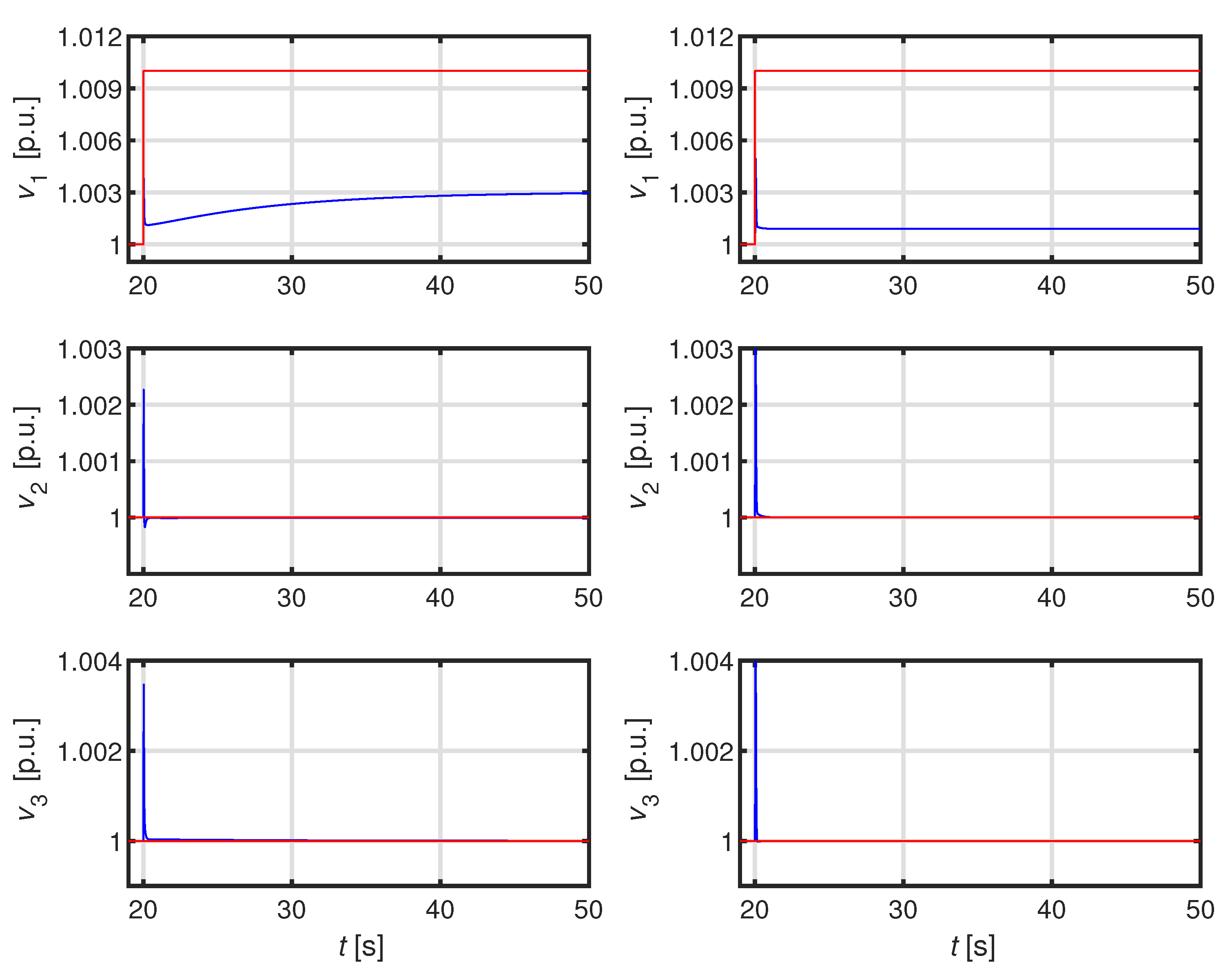
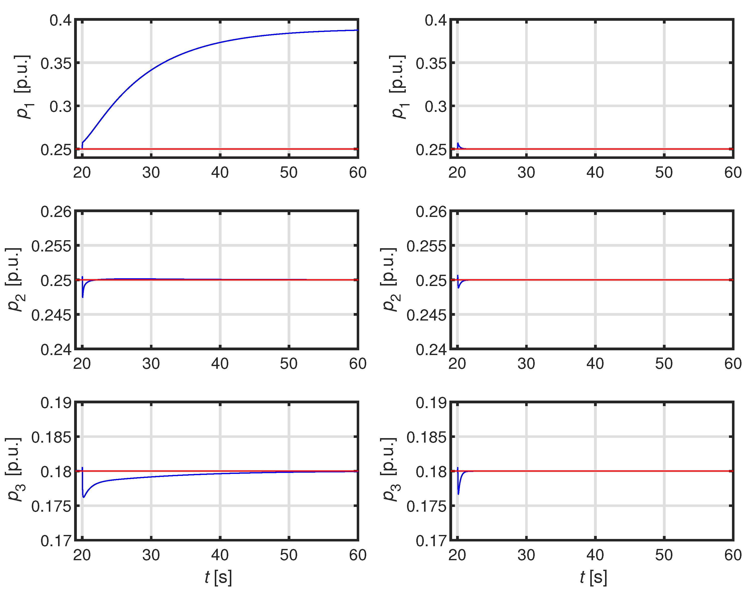
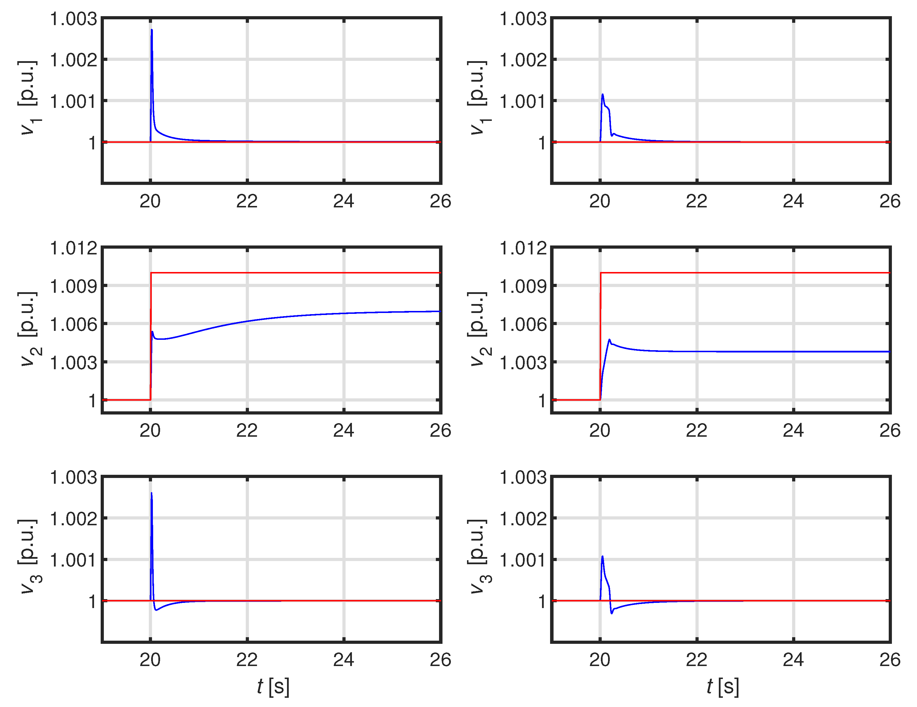
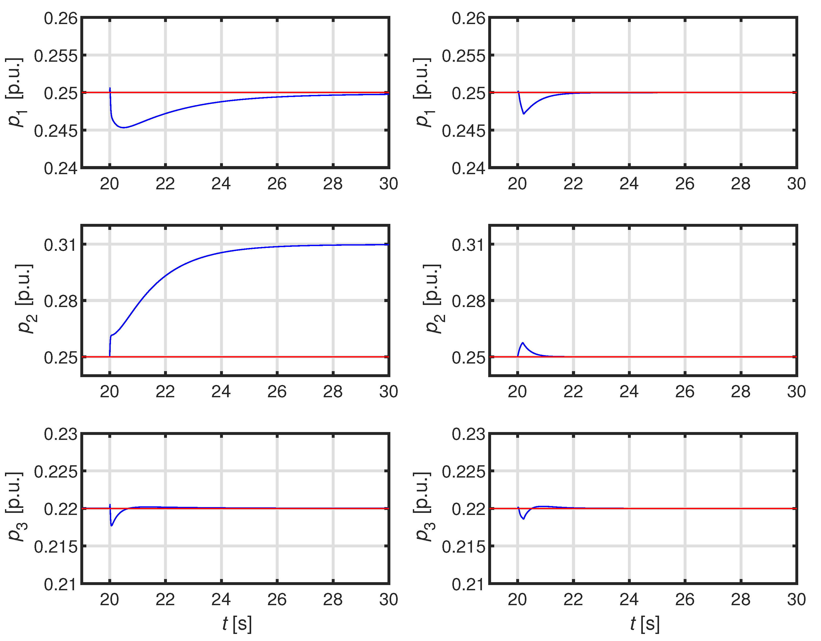
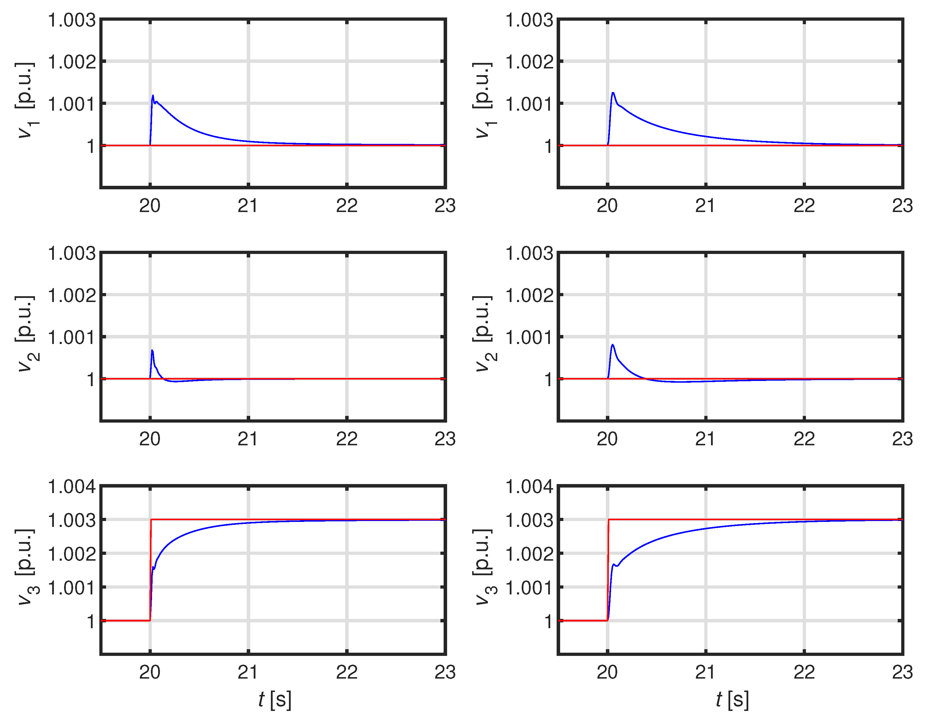
4.1. First Test System: ADN with One Feeder and Three DERs

The one-line electric diagram of the first test system is reported in Figure 3. An MV/LV transformer (250 kVA rated power, 20/0.4 kV rated voltage) connected to an MV busbar (slack node 1) supplies the LV substation busbar (node 2) from which a single LV feeder with two laterals departs. The electrical parameters of the lines are reported in Table 1 together with the loads at the end of each line (represented by the shunt arrows in Figure 3). The total rated load of the feeder is equal to 39.0 kW–19.5 kVAR.
Three DERs are connected to the LV feeder to, respectively, nodes 6, 11, and 13. Each DER is composed of a 35 kWp PV equipped with a battery storage system sized 24 kWh/1 h and connected to the grid by a single inverter with a rated power equal to 50 kVA. The DER provides flexibility to the DSO by varying the injected active power with respect to the one generated by the PV through the storage and by varying the reactive power within the rectangular capability curve of the inverter, that is within the range ± 30 kVAR. Each DER is connected to the distribution system through an AC filter equipped with a 4 kVAR capacitor and a 50 kVA transformer.
To apply the proposed design procedure, an operating condition of the ADN is assumed; the details are as follows: null power injections of DERs; 70 % loading conditions and balanced loads; unitary per-unit values for both voltage at the slack node and ratio of the substation transformer. For this condition, the ADN model is derived yielding the nominal plant matrix P n ( s ) = T n G ( s ) . Then, the first step in the design is performed to obtain the voltage control matrices: each C v i ( s ) is designed for model P i e o t f ( s ) ( i = 1 , 2 , 3 ) obtained by (8). Parameters λ v 1 , λ v 2 , and λ v 3 are obtained by solving problem (10) with λ v i m = 0.06 , λ v i M = 0.3 , and Ω v = [ 0.01 50 ] . In particular, the imposed values for λ v i m and λ v i M guarantee typical values of the pulse bandwidth. Problem (10) is solved by the sequential quadratic programming algorithm of the fmincon function available in the MATLAB library. This function realizes nonlinear programming and treats all variables as continuous. The voltage control matrix obtained by (9) is as follows:
C v ( s ) = diag 14.195 ( s + 83.95 ) s 17.287 ( s + 78.06 ) s 13.768 ( s + 79.78 ) s
which is indeed a PI control.
With regard to the design of C p i ( s ) and ω f i , it is set that d r i = 20 , β = 10 ; α 1 i = 2 , α 2 i = 6 , α 3 i = 2 10 2 , and α 4 i = 1 . Subsequently, parameters λ p 1 and ω f 1 are obtained by solving problem (16). The same design procedure is repeated for λ p 2 , ω f 2 and λ p 3 , ω f 3 . The active power control matrix calculated using (13) is
C p ( s ) = diag 0.0074595 ( s + 90.92 ) s 0.03014 ( s + 88.51 ) s 0.010391 ( s + 83.34 ) s
which is indeed a PI control. Moreover, the following are obtained:
D r 1 ( s ) = 20 1.183 s + 1 11.83 s + 1 D r 2 ( s ) = 20 0.3 s + 1 3.0 s + 1 D r 3 ( s ) = 20 0.909 s + 1 9.09 s + 1
The described design technique assumes that T n is a constant matrix; however, its value depends on factors such as the power injected through the DERs, the power consumed by the loads at each node, the topology of the distribution system, etc. Hence, in the presence of uncertainty in the elements of matrix T , it is necessary to investigate the robust stability of the control system. To this aim, a matrix T has been determined for each one of the considered operating conditions. In particular, the following ones have been considered: the reactive power ranges in the interval [ 0.015 0.015 ] pu; the voltage at the slack bus varies in the interval [ 0.98 1.02 ] pu; and loads in the range [ 0.3 1.2 ] . At the end of the procedure, a set formed by 180 different matrices T (also including T n ) has been created leading to 180 different matrix plant P ( s ) . Subsequently, for any P ( s ) , the corresponding MIMO closed-loop matrix
W ( s ) = I + P ( s ) C ( s ) 1 P ( s ) C ( s )
with
C ( s ) = diag C p 1 ( s ) C v 1 ( s ) C p 2 ( s ) C v 2 ( s ) C p 3 ( s ) C v 3 ( s )
is built, and the largest pole is computed. The obtained set formed by the 180 poles is shown in Figure 4. One can see that the requirement of robust stability is always fulfilled.
To illustrate the performance of the proposed control design (referred to here as the proposed control), simulation results are compared with the ones obtained from the application of the method presented in [30] in the absence of the active power ancillary service, that is d r i = 0 (referred to here as the standard control). The time evolution of the DER nodal voltages and injected active power is analyzed when imposing, for each DER at a time, a step variation in the desired voltage signal v d e s i at a simulation time instant t = 20 s. In particular, Figure 5 and Figure 6 refer to a step variation of v d e s 1 of DER 1 from 1.0 to 1.01 p.u., Figure 7 and Figure 8 to a step variation of v d e s 2 of DER 2 from 1.0 to 1.01 p.u., and Figure 5 and Figure 6 to a step variation of v d e s 3 of DER 3 from 1.0 to 1.003 p.u. Each figure shows the time evolution of either the voltages or the active powers for the three DERs, comparing the responses of the proposed control on the left side with the corresponding ones of the standard control on the right side.
From the analysis of Figure 5 and Figure 6, focusing on DER 1 , it is apparent that the voltage v 1 does not reach the new desired value equal to 1.01 p.u. due to reactive power saturation. Comparing the two controls, the proposed control guarantees a smaller voltage error, reaching a value of about 1.003 p.u. with respect to the standard control, which reaches a value of about 1.001. This result is due to the action of active power according to the ancillary service characterized by d r i = 20 ; in fact, the active power varies from 0.25 p.u., which is the desired value, to about 0.39 p.u., which is the new final value, so as to reduce the voltage error. Regarding the other DERs, it is evident that the voltage control promptly reacts to the variation in the reactive power injection by DER 1 in the first instants before its saturation. Then, the standard control is practically inactive, whereas the proposed control presents a slight reaction in terms of active power in response to the slow voltage variation in v 1 ; it is more evident for DER 3 , which is more strongly coupled with DER 1 than DER 2 .
Similar considerations are derived from the analysis of Figure 7 and Figure 8 in the case of a step variation of v d e s 2 of DER 2 . Also in this case, the voltage v 2 does not reach the new desired value equal to 1.01 p.u. due to reactive power saturation, and the proposed control guarantees a smaller voltage error than the one obtained by the standard control due to the action of active power, which varies from 0.25 p.u. to about 0.31 p.u. Regarding the other DERs, the voltage control promptly reacts to the variation in the reactive power injection by DER 2 in the first instants before its saturation. In this case, the smaller scale on the time axis allows a comparison of the voltage transients according to the following details: for the proposed control, the voltage response is slightly faster, but the variation is slightly larger with respect to the standard control. Regarding the active power of the other DERs, the presence of the ancillary service causes, as expected, a slightly larger and slower perturbation in the active powers (it is more evident for DER 1 ). However, it can be stated that the variation is well limited by the filter and by the action of the active power controller. As a general consideration, it can be stated that the response of the controllers of DER 2 is faster than that of the controllers of DER 1 as analyzed in the previous case; this result is due to the weak coupling of DER 2 with the other two DERs that allows the design procedure to give smaller values of λ v i , λ p i and a larger value of ω f i .
Finally, in the case of DER 3 (Figure 9 and Figure 10), a smaller step variation of v d e s 3 is imposed to avoid reactive power saturation and to analyze the transient responses of the controllers in linear operation. In fact, the voltage v 3 reaches the new desired value equal to 1.003 p.u., and both the proposed and standard control guarantee null steady-state voltage error. Then, the active power does not provide any ancillary service to voltage regulation, and all the active powers return to their desired steady-state values. By analyzing the transients, Figure 9 shows the faster voltage response guaranteed by the proposed control with respect to the standard control. It is due to the active power, which contributes to the voltage regulation during the transient response, as shown in Figure 10. It is important to note from this figure that the active power contribution during transient is negligible in terms of energy injected/absorbed by the storage system; in fact, the energy is represented by the integral of the active power whose variation is limited to less than 0.01 p.u. and lasts for a few seconds.

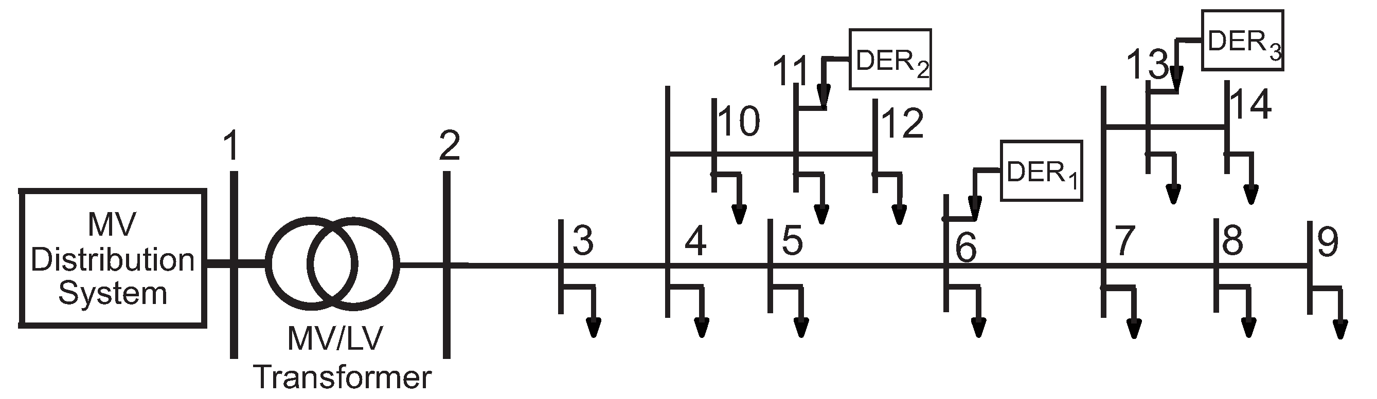
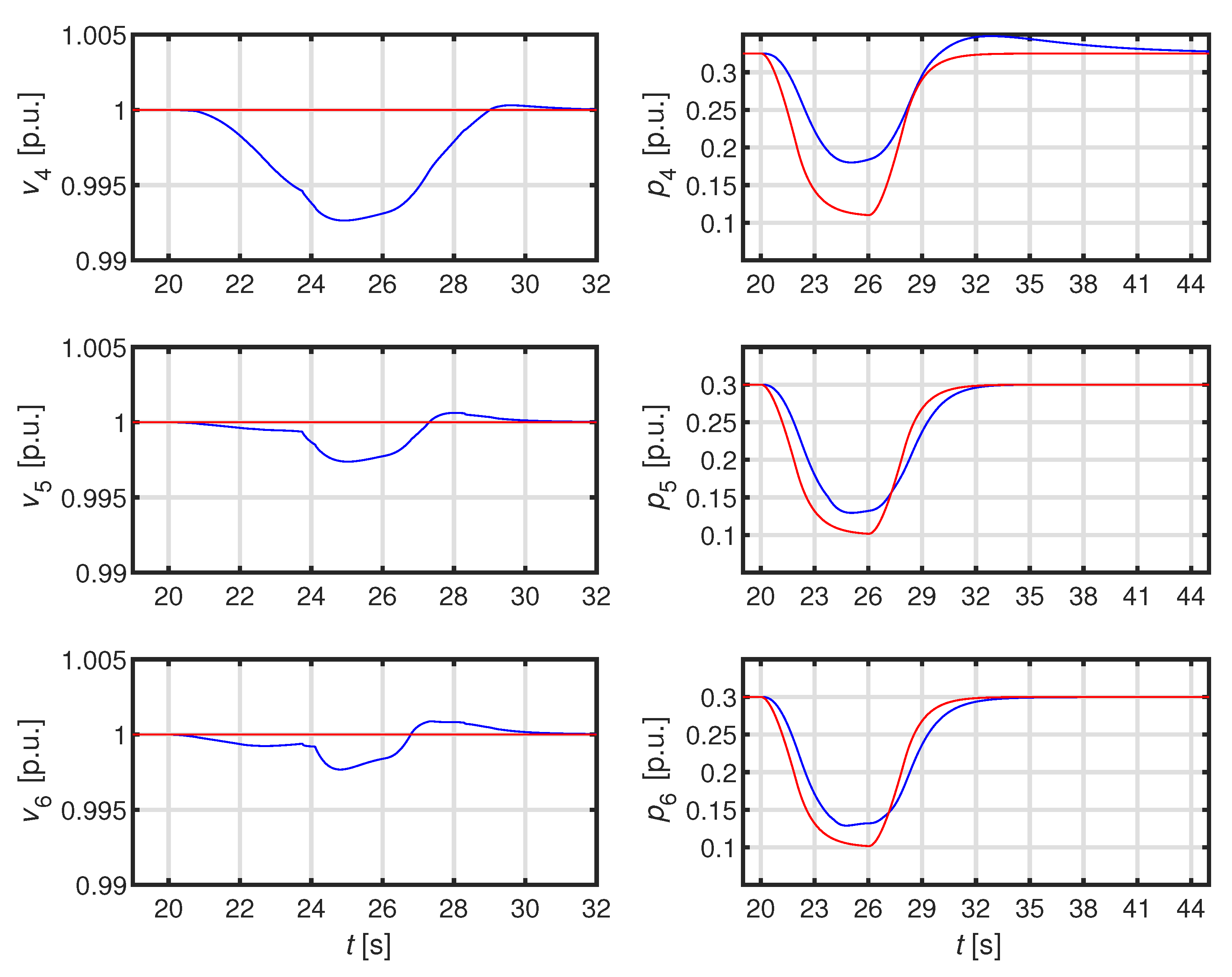
4.2. Second Test System: ADN with Three Feeders and Nine DERs

To show the applicability of the proposed control, a larger distribution network (0.4 kV–50 Hz) is considered, see [31]: it has three feeders, thirty-six nodes and nine DERs connected. Each DER presents the same size and characteristics as the ones described in the previous subsection for the first test system. The results obtained in three simulations are reported to analyze the effects of, respectively, a load insertion (Simulation 1), variations in the desired active power signals due to changes in the solar radiation (Simulation 2), and the On-Load Tap Changer (OLTC) operation in the MV/LV substation (Simulation 3).

4.2.1. Simulation 1: Large Load Connection

At simulation time instant t = 20 s, a load of 20 k–10 kVAR is connected at the end of the first feeder. Figure 11 reports the time evolution of the nodal voltage (left-hand side) and the active power (right-hand side) for DER 1 , DER 2 , and DER 3 , which are connected along the first feeder. The response of the proposed control to the sudden decrease in the nodal voltages due to the load connection is stable and fast, reaching the new steady-state operation in a few seconds. In particular, DER 1 and DER 3 show saturated reactive power, and consequently the ancillary service acts by increasing the injected active power thus reducing the steady-state voltage error.

4.2.2. Simulation 2: Time-Varying Irradiation

In this simulation, a variation in the desired active power signal is imposed during the simulation time interval t = 20–30 s. In particular, due to the shading effect of a cloud, it is assumed that the signals v d e s 4 , v d e s 5 , and v d e s 6 of, respectively, DER 4 , DER 5 , and DER 6 along the second feeder are temporarily reduced down to 0.1 p.u. Figure 12 reports the time evolution of the nodal voltage (left-hand side) and the active power (right-hand side) for the three considered DERs. In the case of DER 4 , the voltage decreases down to about 0.993: this result is due to saturation of the reactive power as evidenced by the active power, which decreases but keeps larger values than the desired signal so as to support the voltage and limit its decrease. On the contrary, in the case of DER 5 and DER 6 , the reactive power does not saturate, except for the very small time interval around t = 24–26 s when the active power is very low. Consequently, with respect to DER 4 , the voltage variations are more limited and the injected active power better follows the desired signal.

4.2.3. Simulation 3: Variation in the Substation Transformer Ratio

In this simulation, step variations in the MV/LV transformer ratio are operated by the OLTC in the feeding substation. In particular, during the simulation time interval t = 20–25 s, six step increases in the OLTC take place, one per second, causing an overall variation in the transformer ratio from 1.0 to 1.0375 p.u. Figure 13 reports the time evolution of the nodal voltage (left-hand side) and active power (right-hand side) for the three considered DERs, namely, DER 7 , DER 8 , and DER 9 . Also, this simulation shows the stable fast responses of the proposed controllers. Regarding the ancillary service, DER 7 starts from an operating condition of reactive power saturation: the nodal voltage is smaller than the desired value equal to 1.0 p.u., and the injected active power is equal to 0.33 p.u., which is larger than the desired value equal to 0.3 p.u. Then, the effect of the OLTC operation causes an increase in the nodal voltage and allows the voltage regulation to guarantee the desired value without the need for the ancillary service; in fact, the active power injection reaches the final steady-state value equal to the desired one. Regarding DER 8 , its behavior is the opposite: it starts from a null voltage and active power errors, but the voltage increase due to the OLTC operation causes the reactive power to decrease and reach its negative saturation. Consequently, the final steady-state operation shows a voltage that is larger than the desired value equal to 1.0 p.u., and the action of the ancillary service causes the active power to reach a steady-state value of about 0.167 p.u., which is smaller than the desired value equal to 0.2 p.u. Eventually, DER 9 does not reach reactive power saturation and shows null steady-state errors for both voltage and active power and both before and after OLTC operation.

5. Conclusions

This paper has proposed a decentralized control of DERs providing the ancillary service of voltage regulation. The goal is to achieve local voltage regulation by each DER, which acts on its reactive power injection and, in the case of the inverter current saturation, on its active power injection. The proposed procedure is based on a two-step sequential design: for each DER, two free parameters of a double IMC-PI control loop and the cut-off frequency of a low-pass filter are obtained by minimizing the infinity norm of the matrices modeling the internal and the external interaction among the other control loops. Consequently, the design robustly guarantees voltage and active power regulation with attenuation of the coupling level. The results of different numerical case studies have confirmed the effectiveness of the design technique. Future developments will investigate the use of a multi-agent-based approach to handle the presence of current saturation.

Author Contributions

Conceptualization, G.F. and M.R.; Methodology, G.F. and M.R.; Validation, G.F. and M.R.; Formal analysis, G.F.; Investigation, G.F. and M.R.; Data curation, G.F. and M.R.; Writing—original draft, G.F. and M.R.; Writing—review & editing, G.F. and M.R.; Visualization, G.F. and M.R.; Supervision, G.F. and M.R.; Project administration, M.R. All authors have read and agreed to the published version of the manuscript.

Funding

This research is financially supported by the Project “Ecosistema dell’innovazione-Rome Technopole” financed by the EU in NextGenerationEU plan through MUR Decree n. 1051 23.06.2022—CUP H33C22000420001.

Data Availability Statement

The original contributions presented in the study are included in the article, further inquiries can be directed to the corresponding author.

Conflicts of Interest

The authors declare no conflict of interest.

Abbreviations

The following abbreviations are used in this manuscript:
ADNActive Distribution Network
APCActive Power Curtailment
ASAncillary Service
BESSBattery Energy Storage System
DERDistributed Energy Resource
DGDistributed Generation
DSODistribution System Operator
EOTFEffective Open-Loop Transfer Function
EVElectric Vehicle
IMCInternal Model Control
MIMOMulti-Input Multi-Output
PIProportional Integral
RESRenewable Energy Source
RGARelative Gain Matrix
TITOTwo-Input Two-Output
VSCVoltage Source Converter

References

  1. Olivier, F.; Aristidou, P.; Ernst, D.; Cutsem, T.V. Active Management of Low-Voltage Networks for Mitigating Overvoltages Due to Photovoltaic Units. IEEE Trans. Smart Grid 2016, 7, 926–936. [Google Scholar] [CrossRef]
  2. Ceylan, O.; Paudyal, S.; Pisica, I. Nodal Sensitivity-Based Smart Inverter Control for Voltage Regulation in Distribution Feeder. IEEE J. Photovolt. 2021, 11, 1105–1113. [Google Scholar] [CrossRef]
  3. Almasalma, H.; Deconinck, G. Robust Policy-Based Distributed Voltage Control Provided by PV-Battery Inverters. IEEE Access 2020, 8, 124939–124948. [Google Scholar] [CrossRef]
  4. Zhang, Z.; Dou, C.; Yue, D.; Zhang, Y.; Zhang, B.; Li, B. Regional Coordinated Voltage Regulation in Active Distribution Networks with PV-BESS. IEEE Trans. Circuits Syst. II Express Briefs 2023, 70, 596–600. [Google Scholar] [CrossRef]
  5. Gorbachev, S.; Mani, A.; Li, L.; Li, L.; Zhang, Y. Distributed Energy Resources Based Two-Layer Delay-Independent Voltage Coordinated Control in Active Distribution Network. IEEE Trans. Ind. Inform. 2024, 20, 1220–1230. [Google Scholar] [CrossRef]
  6. Gush, T.; Kim, C.H.; Admasie, S.; Kim, J.S.; Song, J.S. Optimal Smart Inverter Control for PV and BESS to Improve PV Hosting Capacity of Distribution Networks Using Slime Mould Algorithm. IEEE Access 2021, 9, 52164–52176. [Google Scholar] [CrossRef]
  7. Cheng, Z.; Wang, L.; Zeng, S.; Su, C.; Zhang, R.; Zhou, W. Partition-Global Dual-Layer Collaborative Voltage Control Strategy for Active Distribution Network with High Proportion of Renewable Energy. IEEE Access 2024, 12, 22546–22556. [Google Scholar] [CrossRef]
  8. Zhang, Z.; Mishra, Y.; Dou, C.; Yue, D.; Zhang, B.; Tian, Y.C. Steady-State Voltage Regulation with Reduced Photovoltaic Power Curtailment. IEEE J. Photovolt. 2020, 10, 1853–1863. [Google Scholar] [CrossRef]
  9. Xu, S.; Xue, Y.; Chang, L. Review of Power System Support Functions for Inverter-Based Distributed Energy Resources- Standards, Control Algorithms, and Trends. IEEE Open J. Power Electron. 2021, 2, 88–105. [Google Scholar] [CrossRef]
  10. Oureilidis, K.; Malamaki, K.N.; Gallos, K.; Tsitsimelis, A.; Dikaiakos, C.; Gkavanoudis, S.; Cvetkovic, M.; Mauricio, J.M.; Maza Ortega, J.M.; Ramos, J.L.M.; et al. Ancillary Services Market Design in Distribution Networks: Review and Identification of Barriers. Energies 2020, 13, 917. [Google Scholar] [CrossRef]
  11. do Prado, J.C.; Qiao, W.; Qu, L.; Agüero, J.R. The Next-Generation Retail Electricity Market in the Context of Distributed Energy Resources: Vision and Integrating Framework. Energies 2019, 12, 491. [Google Scholar] [CrossRef]
  12. Sun, Y.; Zhao, Z.; Yang, M.; Jia, D.; Pei, W.; Xu, B. Overview of energy storage in renewable energy power fluctuation mitigation. CSEE J. Power Energy Syst. 2020, 6, 160–173. [Google Scholar] [CrossRef]
  13. Gui, E.M.; MacGill, I. Typology of future clean energy communities: An exploratory structure, opportunities, and challenges. Energy Res. Soc. Sci. 2018, 35, 94–107. [Google Scholar] [CrossRef]
  14. Barr, J.; Majumder, R. Integration of Distributed Generation in the Volt/VAR Management System for Active Distribution Networks. IEEE Trans. Smart Grids 2015, 6, 576–586. [Google Scholar] [CrossRef]
  15. Eggli, A.; Karagiannopoulos, S.; Bolognani, S.; Hug, G. Stability analysis and design of local control schemes in active distribution grids. IEEE Trans. Power Syst. 2020, 36, 1900–1909. [Google Scholar] [CrossRef]
  16. Kazeminejad, M.; Banejad, M.; Annakkage, U.; Hosseinzadeh, N. The effect of high penetration level of distributed generation sources on voltage stability analysis in unbalanced distribution systems considering load model. J. Oper. Autom. Power Eng. 2019, 7, 196–205. [Google Scholar]
  17. Ranamuka, D.; Agalgaonkar, A.; Muttaqu, K. Online Voltage Control in Distribution Systems with Multiple Voltage Regulating Devices. IEEE Trans. Sustain. Energy 2014, 5, 617–628. [Google Scholar] [CrossRef]
  18. Cavraro, G.; Carli, R. Local and distributed voltage control algorithms in distribution networks. IEEE Trans. Power Syst. 2017, 33, 1420–1430. [Google Scholar] [CrossRef]
  19. Nawaz, F.; Pashajavid, E.; Fan, Y.; Batool, M. A Comprehensive Review of the State-of-the-Art of Secondary Control Strategies for Microgrids. IEEE Access 2023, 11, 102444–102459. [Google Scholar] [CrossRef]
  20. Bedawy, A.; Yorino, N.; Mahmoud, K.; Lehtonen, M. An Effective Coordination Strategy for Voltage Regulation in Distribution System Containing High Intermittent Photovoltaic Penetrations. IEEE Access 2021, 9, 117404–117414. [Google Scholar] [CrossRef]
  21. Duan, J.; Wang, C.; Xu, H.; Liu, W.; Xue, Y.; Peng, J.C.; Jiang, H. Distributed control of inverter-interfaced microgrids based on consensus algorithm with improved transient performance. IEEE Trans. Smart Grid 2019, 10, 1303–1312. [Google Scholar] [CrossRef]
  22. Fu, A.; Cvetković, M.; Palensky, P. Distributed Cooperation for Voltage Regulation in Future Distribution Networks. IEEE Trans. Smart Grid 2022, 13, 4483–4493. [Google Scholar] [CrossRef]
  23. Kryonidis, G.; Kontis, E. A Coordinated Droop Control Strategy for Overvoltage Mitigation in Active Distribution Networks. IEEE Trans. Smart Grid 2018, 9, 5260–5270. [Google Scholar] [CrossRef]
  24. Bolognani, S.; Carli, R.; Cavraro, G.; Zampieri, S. On the need for communication for voltage regulation of power distribution grids. IEEE Trans. Control Netw. Syst. 2019, 6, 1111–1123. [Google Scholar] [CrossRef]
  25. Reno, M.J.; Quiroz, J.E.; Lavrova, O.; Byrne, R.H. Evaluation of communication requirements for voltage regulation control with advanced inverters. In Proceedings of the 2016 North American Power Symposium (NAPS), Denver, CO, USA, 18–20 September 2016; pp. 1–6. [Google Scholar]
  26. Wu, X.; Deng, S.; Yuan, W.; Mei, S. A Robust Distributed Secondary Control of Microgrids Considering Communication Failures. In Proceedings of the 2022 4th International Conference on Power and Energy Technology (ICPET), Xining, China, 28–31 July 2022; pp. 395–400. [Google Scholar]
  27. Sadnan, R.; Dubey, A. Distributed optimization using reduced network equivalents for radial power distribution systems. IEEE Trans. Power Syst. 2021, 36, 3645–3656. [Google Scholar] [CrossRef]
  28. Antoniadu-Plytaria, K.; Kouveliotis-Lysikatos, I.; Georgilakis, P.; Hatziargyriou, N. Distributed and Decentralized Voltage Control of smart Distribution Networks: Models, Methods, and Future Research. IEEE Trans. Smart Grid 2017, 8, 2999–3008. [Google Scholar] [CrossRef]
  29. Vu, T.; Lee, M. Independent design of multi-loop PI/PID controllers for interacting multivariable processes. J. Process Control 2010, 20, 922–933. [Google Scholar] [CrossRef]
  30. Vu, T.N.L.; Lee, J.; Lee, M. Design of multi-loop PID controllers based on the generalized IMC-PID method with Mp criterion. Int. J. Control Autom. Syst. 2007, 5, 212. [Google Scholar]
  31. Fusco, G.; Russo, M.; Casolino, G.M. Voltage and active power local PI control of distributed energy resources based on the effective transfer function method. Int. J. Electr. Power Energy Syst. 2023, 152, 1–15. [Google Scholar] [CrossRef]
  32. Fusco, G.; Russo, M. A Decentralized Approach for Voltage Control by Multiple Distributed Energy Resources. IEEE Trans. Smart Grid 2021, 12, 3115–3127. [Google Scholar] [CrossRef]
  33. Albertos, P.; Antonio, S. Multivariable Control Systems: An Engineering Approach; Springer: London, UK, 2004. [Google Scholar]
  34. Manitoba HVDC Research Centre. PSCAD User’s Guide; Manitoba Hydro International Ltd.: Winnipeg, MB, Canada, 2018. [Google Scholar]
Figure 1. Schematic representation of a generic ADN with controlled DERs.
Energies 17 01991 g001
Figure 2. Block diagram of the ADN model with the DER control section.
Energies 17 01991 g002
Figure 3. ADN with 1 feeder (14 nodes) and 3 DERs.
Energies 17 01991 g003
Figure 4. Plot of the set formed by the largest pole of any of the 180 matrices W ( s ) .
Energies 17 01991 g004
Figure 5. Step variation of v d e s 1 : time evolution of the voltage amplitude (blue) and the desired signal (red) at DER connection nodes–proposed (left-hand side) vs. standard (right-hand side) control.
Energies 17 01991 g005
Figure 6. Step variation of v d e s 1 : time evolution of the injected active power (blue) and the desired signal (red) for each DER–proposed (left-hand side) vs. standard (right-hand side) control.
Energies 17 01991 g006
Figure 7. Step variation of v d e s 2 : time evolution of the voltage amplitude (blue) and the desired signal (red) at DER connection nodes–proposed (left-hand side) vs. standard (right-hand side) control.
Energies 17 01991 g007
Figure 8. Step variation of v d e s 2 : time evolution of the injected active power (blue) and the desired signal (red) for each DER–proposed (left-hand side) vs. standard (right-hand side) control.
Energies 17 01991 g008
Figure 9. Step variation of v d e s 3 : time evolution of the voltage amplitude (blue) and the desired signal (red) at DER connection nodes–proposed (left-hand side) vs. standard (right-hand side) control.
Energies 17 01991 g009
Figure 10. Step variation of v d e s 3 : time evolution of the injected active power (blue) and the desired signal (red) for each DER–proposed (left-hand side) vs. standard (right-hand side) control.
Energies 17 01991 g010
Figure 11. DER 1 DER 3 in Simulation 1: time evolution of the voltage amplitude (blue) and the desired signal (red) (left-hand side) and of the injected active power (blue) and the desired signal (red) (right-hand side).
Energies 17 01991 g011
Figure 12. DER 4 DER 6 in Simulation 2: time evolution of the voltage amplitude (blue) and the desired signal (red) (left-hand side) and of the injected active power (blue) and the desired signal (red) (right-hand side).
Energies 17 01991 g012
Figure 13. DER 7 DER 9 in Simulation 3: time evolution of the voltage amplitude (blue) and the desired signal (red) (left-hand side) and of the injected active power (blue) and the desired signal (red) (right-hand side).
Energies 17 01991 g013
Table 1. Electrical parameters for the first test system.
From NodeTo NodeR (p.u.)X (p.u.)Load (kW–kVAr)
230.01050.00253.11–1.56
340.00590.00142.05–1.02
450.01140.00272.05–1.02
560.00790.00117.97–3.96
670.00950.00142.05–1.02
780.00530.00073.11–1.56
890.00400.00063.11–1.56
4100.01060.00153.11–1.56
10110.01210.00173.11–1.56
11120.00400.00063.11–1.56
7130.00890.00113.11–1.56
13140.00370.00023.11–1.56
Disclaimer/Publisher’s Note: The statements, opinions and data contained in all publications are solely those of the individual author(s) and contributor(s) and not of MDPI and/or the editor(s). MDPI and/or the editor(s) disclaim responsibility for any injury to people or property resulting from any ideas, methods, instructions or products referred to in the content.

