1. Introduction
At the 2022 United Nations Climate Change Conference, governments were called upon to review and enhance their emissions reduction targets for 2030 in their national climate strategies, while also advocating for an acceleration in the reduction of coal-derived energy use [
1].
Based on the aforementioned goals, there is a notable interest in advancing the technology related to solar cells, with the goal of increasing efficiency in the conversion of light energy into electrical energy. Therefore, the creation of tools that streamline research into these devices emerges as an area of significant importance in the current context.
Within the realm of modeling solar cells and panels, series resistance typically symbolizes the losses associated with different materials and the interaction between them [
2], and its identification is crucial in the modeling process. Typically, this resistance is determined by the slope of the I-V curve in the Voc (open-circuit voltage) region, which is characterized by low currents and high voltages [
3,
4]. However, it is important to note that the movement of electrons, which is responsible for the electric current, is influenced by the various junctions present in a solar cell, including those of the metal-semiconductor and semiconductor-semiconductor [
5,
6].
In this work, a detailed analysis focused on the identification of series resistance (Rs) is presented. This analysis is applied to four solar cell fabrication processes developed at the National Institute of Astrophysics, Optics, and Electronics (INAOE). The different solar cells being analyzed have an area of 1 cm
2 [
7]. This analysis ranges from calculating the series resistance based on semiconductor physics parameters to determining Rs by applying the straight-line slope technique to the I-V curve of each manufactured device.
2. Series Resistance (Rs) Components and c-Si Structure
The most prominent parameter of solar devices is efficiency, as this to some extent determines the quality of the solar cell and its technology. To achieve a high-quality solar cell, it is necessary to minimize potential losses.
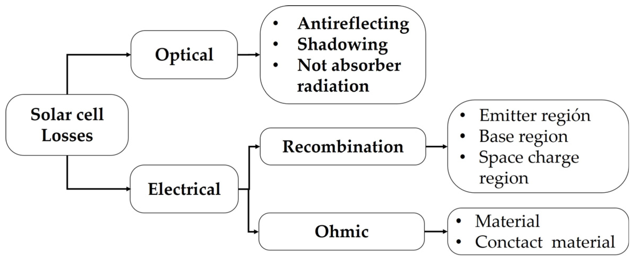
Figure 1 presents a diagram illustrating some of the possible losses in solar cells, which can be classified into two general groups: optical and electrical.
The electrical losses shown in
Figure 1 can be of two types: recombination losses and ohmic losses. In this study, we will focus solely on investigating the latter, specifically those losses associated with the material and metal contacts [
2].
2.1. Influence on the Efficiency of Ohmic Resistances
Solar cells often exhibit parasitic resistances, both in series and shunt. These resistances have a significant and disadvantageous impact on the performance of solar cells as they dissipate energy in the form of heat. In most cases, and for typical values of parallel and series resistances, the primary consequence of parasitic resistance is a reduction in the fill factor and, consequently, the efficiency of the solar cell [
8].
Several physical mechanisms are responsible for the presence of these resistances. The major contribution to series resistance (Rs) comes from the resistance of the semiconductor material constituting the cell, as well as the resistance of the semiconductor material that is in contact with the metallic conductor (metal contacts). Conversely, shunt resistance (Rsh) originates from leakage across the p-n junction around the edge of the cell and in non-peripheral regions, especially in the presence of crystal defects and precipitates formed from foreign impurities in the junction region [
9].
Shunt and series resistances are generally calculated from the slope of the I-V characteristic curve [
10]. In
Figure 2, the effects of each of these resistances on the shape of the curve can be observed.
In
Figure 2a, the impacts on the I-V curve are shown when high values of Rs are present as, ideally, this resistance should tend toward zero.
Conversely, in
Figure 2b, having small values of shunt resistance also results in deformation of the I-V curve as, ideally, this resistance should be as large as possible, tending toward infinity [
2].
2.2. Components of the Series Resistance (Rs)
The series resistance, commonly represented as Rs, generally arises from both the inherent resistance of the semiconductor material forming the solar cell and the resistance of the semiconductor material at the interface with the metal contacts [
9].
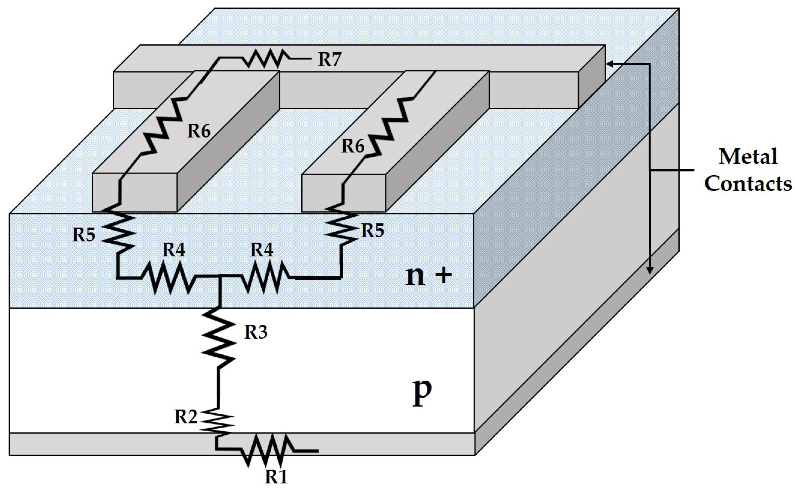
Figure 3 illustrates each of the components of series resistance.
Each of the resistances presented in
Figure 3 represents the following [
2]:
| R1 | Back metal contact |
| R2 | Metal-semiconductor contact across the entire back surface |
| R3 | Semiconductor material (base) |
| R4 | Resistance of the emitter between two grid fingers |
| R5 | The metal-semiconductor contact of the grid finger |
| R6 | Grid finger resistance |
| R7 | Busbar resistance |
To calculate each of the components of Rs, the equations presented in
Table 1 can be used.
The meaning of each term in the equations provided in
Table 1 is available in
Table 2.
To calculate
and
, it is essential to take into consideration the height of the potential barrier generated by the contact between the metal and the semiconductor, considering whether it is of the
n-type or
p-type. For the
n-type case, we have [
2]:
while for the
p-type contact, we have:
where:
| Height of the metal-semiconductor barrier |
| Work function of the metal |
| Work function of the semiconductor |
| Bandgap of the semiconductor |
Once the barrier height has been calculated, it is possible to determine the specific contact resistivity. This resistivity is influenced by the mechanism of the motion of electrons between the metal and the semiconductor. This movement can occur through either the tunneling effect or the thermionic effect, depending on the doping level of the semiconductor.
Therefore, the tunneling effect is given by:
where
A* = the Richardson constant (1.2 × 10
6 A/m
2K
2), and
m* = the mass of the electron.
The thermionic effect can be calculated as:
where
k = the Boltzmann constant,
q = the charge of the electron, and
T = temperature.
2.3. Single-Junction c-Si Solar Cells
In [
7], an INAOE manufacturing process for making solar cells with a simple structure based on c-Si has been detailed.
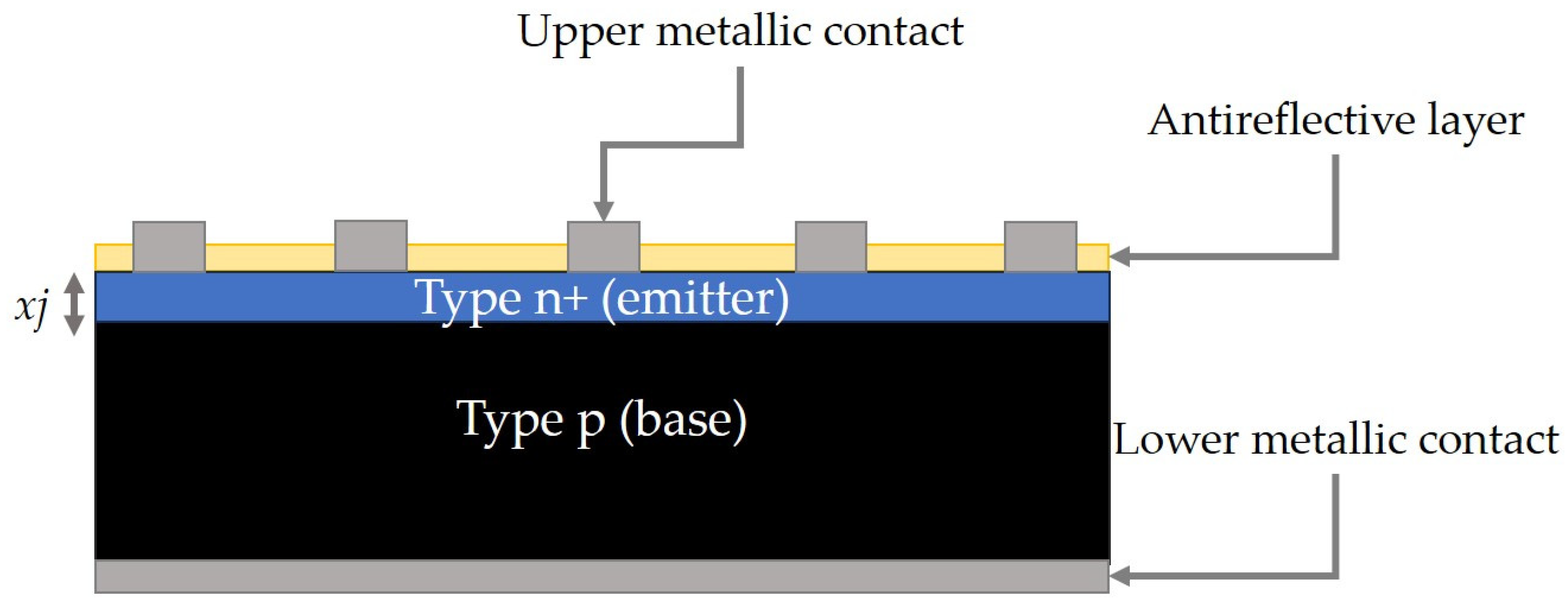
Figure 4 provides a comprehensive illustration of the configuration of these cells.
As shown in
Figure 4, solar cells with a simple structure are basically composed of a p-n+ junction without texturing, an antireflective layer that is usually made of SiO
2, and the upper and lower metal (Al) contacts [
7].
A crucial parameter in these cells is the junction depth (
xj). Therefore, optimizing this factor contributes to achieving better efficiencies since the latter will be directly affected by the series resistance (Rs) [
7].
In a previous study [
8], four manufacturing processes (I–IV) were carried out with the aim of finding the optimal junction depth that would result in the best efficiency, as detailed in
Table 3.
As seen in
Table 3, a variation in junction depth has a direct impact on the efficiency of the solar cell. Changing the depth from 0.87 μm to 0.60 μm results in a 2.4% increase in efficiency.
Influence of Sheet Resistance on the Efficiency of the Solar Cell
The sheet resistance,
RSH, indirectly affects the efficiency of the solar device, depending on the magnitude it can reach and whether it is a uniformly doped substrate or a non-uniformly doped one [
11].
For uniformly doped substrates,
RSH can be determined according to:
where
t = the thickness of the substrate,
= the resistivity of the material, and
σ = the conductivity of the material.
For non-uniformly doped substrates [
8,
11], R
SH can be calculated as:
where
q = the charge of the electron,
xj = the junction depth of the emitter,
μn = electron mobility, and
C(
x)
= the concentration profile.
Conversely, sheet resistance can also be calculated experimentally using the four-point technique. In [
11], this technique is described in greater detail.
As described in previous sections, a solar cell is the junction of two materials, p-n, with the substrate generally being of the p-type. For the emitter, diffusion or ion implantation processes are typically carried out [
8], which, according to Equations (5) and (6), will modify the R
SH of the substrate based on the junction depth between the materials. This implies that R
S will also undergo changes according to these parameters and, in turn, will modify the final cell efficiency as shown in
Table 3.
2.4. Top Contact Grid
A fundamental aspect that significantly influences series resistance (R
S) is the nature of the metallic contacts, as they are responsible for facilitating the flow of electrons from the cell to the load [
12].
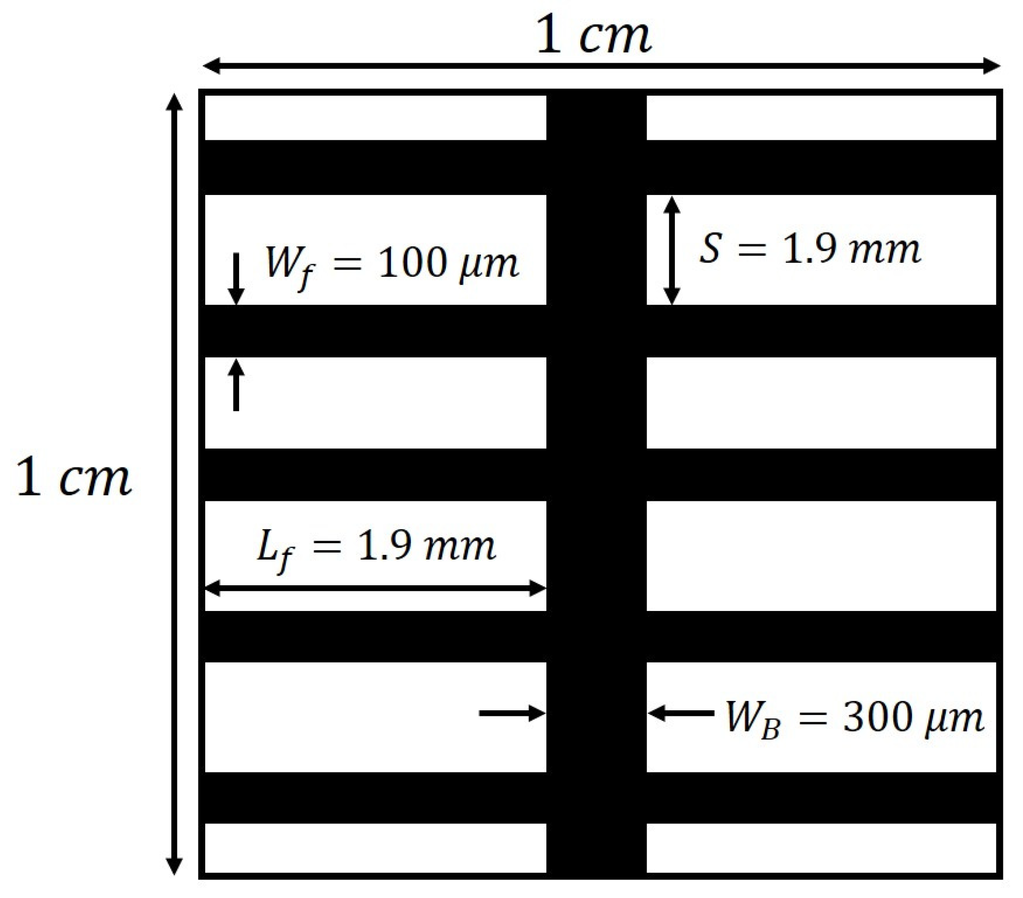
Figure 5 illustrates the configuration of the front grid, which commonly consists of a main bus and transverse collector bars, known as “fingers” [
13].
In
Figure 5, the geometry of the contact grid used for the simple-structured cells described in [
13] is depicted. For the lower contact, typically, a metallic layer is deposited over the entire surface. In specific cases, contact windows are opened, which help to enhance the efficiency of the device.
2.5. Configuration of Resistances for the Calculation of Rs
In the previous section, the components constituting the series resistance (R1–R7), as well as the structural characteristics of the pn junction and the geometry of the top contact grid, have been described.
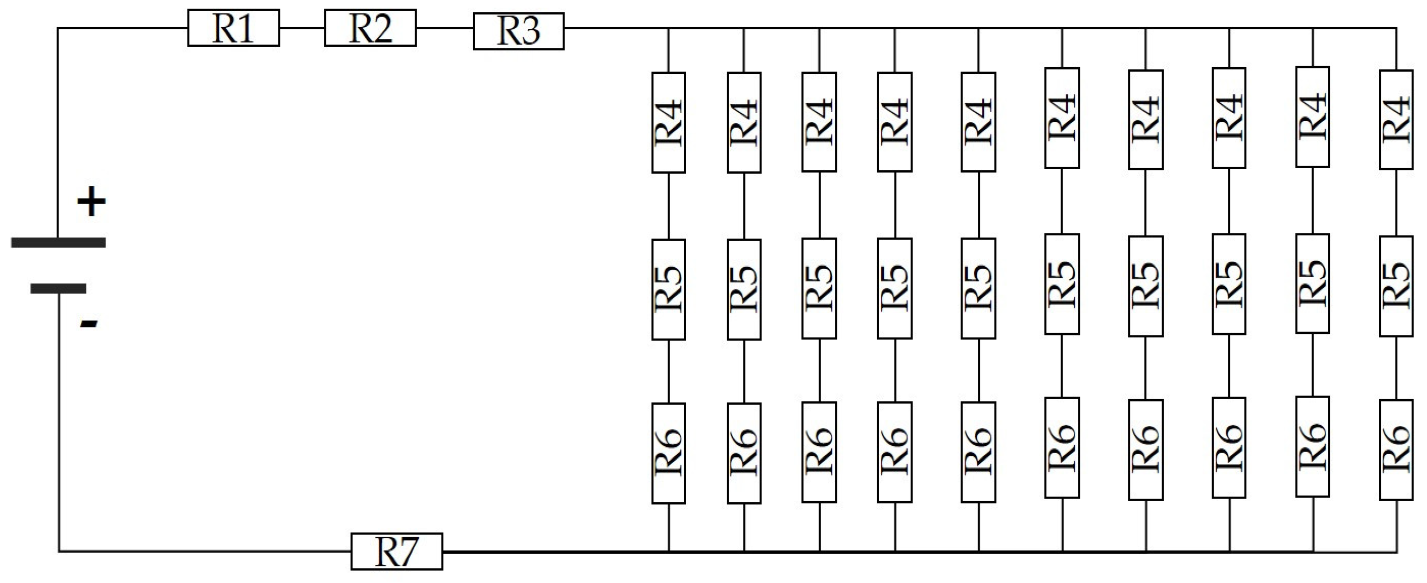
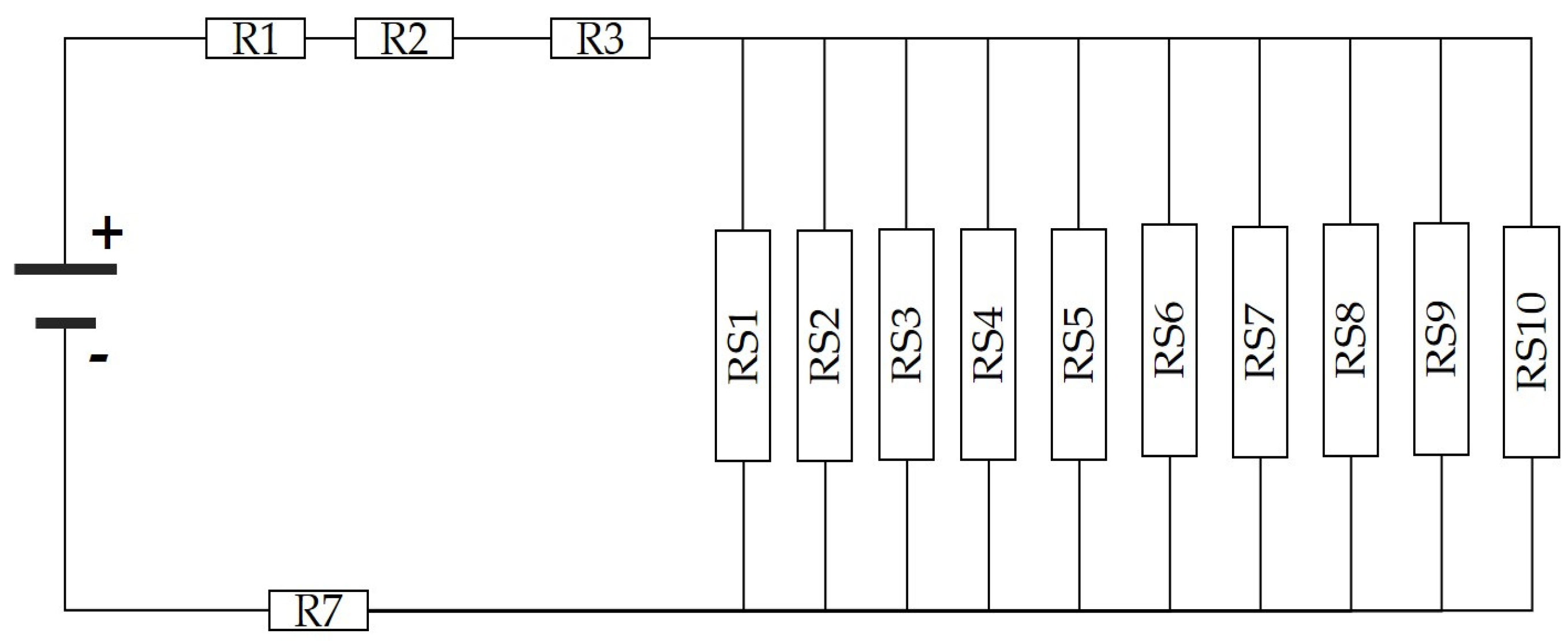
The utilization of a resistor network is proposed to conduct the analysis and calculation of series resistance, as depicted in
Figure 6. This circuitry takes into account the different components given in
Table 1: the contact resistance (metal-semiconductor) generated in each finger of the top grid (R5), the resistance between each grid finger (R4), and the resistance of the grid finger itself (R6). Considering that each finger is connected to the busbar (R7), it is proposed that each resistance generated in R4–R6 is in parallel with the succeeding finger.
In
Figure 6, resistors R1, R2, R3, and R7 represent common resistances associated with the contact with the p-type semiconductor, substrate, busbar, and the rear metal contact, which is shared anywhere in the cell, respectively.
The resistance associated with each finger will be determined by the following equation:
Equation (7) provides a series resistance for each finger, resulting in
,
,
, …,
. With this series resistance, the configuration of the resistor network presented in
Figure 6 is simplified as shown in
Figure 7.
With the new resistor configuration shown in
Figure 7, circuit analysis is once again performed, applying Equation (8), the equivalent resistance
is calculated. This will enable the final calculation of the Rs.
The resulting equivalent resistance (
REq) is shown in the new resistive network of
Figure 8. Through this updated arrangement and by the Equation (9) is applied to simplify the circuit, the value of the series resistance (Rs) of the cell is determined.
With Equation (9), it is possible to calculate the total series resistance, considering all its components from the substrate to the metal contacts.
3. Results
In this section, the calculations to estimate R1–R7 are presented using the equations from
Table 1, along with Equations (1)–(5) and (7)–(9).
Table 4 details the parameters related to both the grid geometry and the properties of the materials (the substrate and the conductive material).
Given that p-type material and n-type material have different properties, the sheet resistance is determined according to Equation (6) using a resistivity of 5 Ω-cm, in the case of the substrate (RSHSUB), and using the four-point technique in the case of the emitter (RSHE).
The variations of R
SHE and R
SHSUB, depending on the junction depth of each manufacturing process, I–IV, are presented in
Table 5.
Table 5 shows how R
SHE and R
SHSUB vary when adjusting
xj. By applying Equation (6) with a resistivity of 5 Ω-cm for the substrate, the thickness of t
sub will be modified based on the junction depth and, consequently, R
SHSUB will change.
Obtaining R
SHSUB using the four-point technique allows us to determine the resistivity of the substrate (
p-type), even without forming the p-n junction.
Table 6 shows the comparison between experimentally obtained R
SHSUB and theoretically calculated R
SHSUB by applying Equation (6). For these calculations, a value of ρ
SUB of 8.5 Ω-cm was used, generating a discrepancy in R
SHSUB of less than 3%. Nevertheless, it is evident that the application of Equation (6) is effective for calculating R
SH in situations where the substrate is uniformly doped.
Using the experimental resistivity values, calculations for the components of the series resistance (R1–R7) are carried out, considering both R
SH for each side of the cell and R
SHSUB and R
SHE for the substrate and emitter, respectively. These calculations take into account that these components are affected by the junction depth in each process.
Table 7 presents the results obtained for each of these components.
Table 7 displays the results derived from the application of the equations detailed in
Table 1. It can be observed that R
SHSUB and R
SHE vary with the junction depth, directly impacting those components dependent on these parameters.
R3 is not directly linked to RSHSUB but depends on the thickness of the p-region (tPR), the value of which is modified according to the depth of the emitter, ranging between 0.87 µm and 0.60 µm.
R1, R6, and R7, depending on the grid geometry and conductor thickness, remain unchanged with any changes in R
SH. Their resistance stays constant and is only presented in the first section of
Table 7 for a depth of 0.87 µm.
The calculations made to determine the series resistance are based on the equations presented in
Section 2.5.
Once REq is obtained, it is possible to apply Equation (9) to obtain the series resistance of the solar cell.
Table 8 shows how the series resistance varies with junction depth, confirming that a decrease in
xj results in a reduction in series resistance, demonstrating the influence of R
SH on total Rs.
The calculation of series resistance, as outlined in
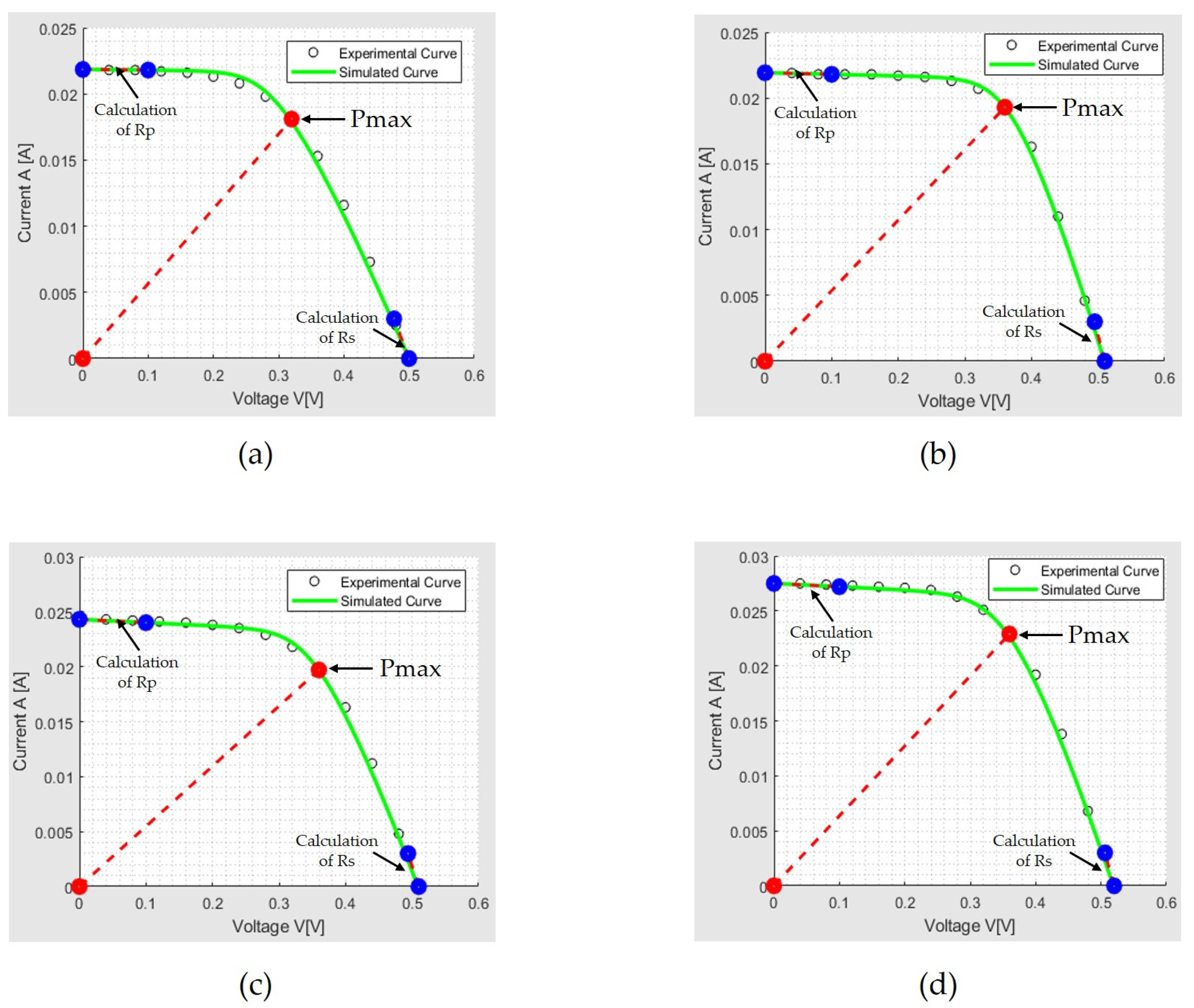
Table 8, is juxtaposed with a method for determining this resistance through parameter extraction (see
Figure 9), as further expounded in reference [
14]. This approach entails computing the slope of the solar device’s I-V curve within the V
OC region, where series resistance exerts a notable influence. Furthermore,
Table 8 provides a comprehensive account of the percentage variance between the aforementioned calculations and those derived using the parameter extraction technique.
Table 8 indicates that in each case of efficiency improvement, the series resistance tends to decrease, in accordance with the theory outlined in
Section 2.1 of this work. Although the differences between theoretical Rs and that obtained by parameter extraction may seem “high”, this could be due to the conditions under which the cells were obtained or characterized for the I-V curve. Nevertheless, it is demonstrated that the Rs calculation follows a similar behavior to that of the parameter extraction model.
Figure 9 presents the experimental curves obtained for each cell as a function of junction depth (
xj), with which the series resistance (Rs) was calculated.
Table 9 provides the performance parameters for each cell corresponding to the specific junction depth,
xj.
Table 9 highlights how the reduction in junction depths improves the performance parameters of the solar cell, particularly emphasizing a greater influence on the short-circuit current (I
SC). This phenomenon can be attributed to the decrease in the distance that charge carriers (electrons and holes) generated by sunlight must travel before being captured by the electrical contacts of the cell. As a result, recombination losses are reduced, and the current generated by the cell increases [
7,
15].
4. Discussion
In a study conducted by the authors of [
16], the optimization of the top contact grid is addressed with a limited focus, as the study solely concentrates on that part and generalizes a system of equations based on the number of buses that the top contact can contain. However, it does not delve into other elements of series resistance. While it presents a proposal for an arrangement of resistances that considers all the components in series, this approach only works within the scope of that study by not analyzing the substrate’s characteristics and by considering only the upper metallic contact.
In [
17], c-Si cells are examined, with an emphasis on optimizing the fingers that make up the grid to minimize the losses caused by partial or total shading. Although the components of series resistance are generally mentioned, the study focuses solely on increasing the width or height of two of the grid fingers through the use of aluminum and silver deposits as metallic contacts.
In a previous study [
18], the investigation focuses on PERL and LGBC-type cells, addressing the components of series resistance. However, the analysis specifically centers on the metal-semiconductor contact in the front grid and the contact windows on the rear. It discusses how the implementation of high doping and the use of a low-resistivity conductor, such as silver, contribute to improving the efficiency of the solar cell in these regions. Despite these observations, there is no explicit presentation of an equivalent circuit that models the losses associated with series resistance. Overall, the research is concentrated on analyzing metallization techniques to achieve optimal metal-semiconductor contact.
In [
19], the components of series resistance (Rs) in silicon (Si) solar cells are examined. However, it is noted that these components are once again considered to be all in series, resulting in high values of Rs in the calculations performed. Later in the same study, the conditions for determining Rs are modified; however, this process is carried out using Ohm’s law and not through the components that were initially described.
Contrary to these cases, the present work demonstrates that for a simple-structured cell, factors other than metallic contacts influence Rs, such as junction depth, which alters the properties of p-n materials, modifying the RSH, which is also part of the final Rs. Additionally, a circuit is proposed that models the components of Rs, considering it as series resistance without assuming that all its components are in series as well.
5. Conclusions
The current study establishes that series resistance (Rs) is not exclusively confined to the front metal contacts (grid), as commonly asserted. It has been demonstrated that additional factors, such as junction depth (
xj), which influence sheet resistance (R
SH) are an integral part of the manufacturing process. The consideration of R
SH is critical, as elevated values of this component lead to increased Rs values. In [
9], there is a proposal for the use of substrates with a thickness of 100 μm, as such substrates achieve heightened efficiencies.
The cells employed in this research exhibit a simple structure lacking surface texturing or rear contact windows, providing a baseline for future analyses of more intricate cells. Furthermore, a resistor arrangement is introduced to model the distinct components of series resistance. While this model serves as an initial approximation, displaying acceptable and theory-consistent outcomes, it can be refined in subsequent studies to better accommodate more complex cell structures.
In summary, this study contributes to our understanding of the various parameters constituting series resistance, impacting solar cell efficiency by modifying any of these factors. The broad assumption that only metal contacts are responsible for the losses associated with Rs in solar cells is deliberately avoided.
