Abstract
The phase circulating current (PCC) of the parallel three-phase inverter systems dramatically affects the power quality and conversion efficiency of the power grid. In this paper, a composite suppression strategy is proposed to solve the PCC issue by using the sliding mode control (SMC) approach and improved virtual impedance droop control. Taking the commonly used 2-group parallel three-phase inverter as an example, an inter- and intra-classification model is established by analyzing the sources of PCC. In order to suppress the inter-PCC, the traditional virtual impedance droop control is given, following the improved substitute by combining SMC. And the variables of the bus voltage, Q-U loop, P-f loop, and the virtual-induced reactance are also introduced for the robust control of the impedance droop. On the other side, a SMC-based suppression approach is designed to solve the issue of the intra-PCC. Its idea is to introduce a regulation factor for the space vector pulse width modulation (SVPWM) so that the zero-sequence voltage can be eliminated and the influence of the intra-PCC can be relieved. Comparative simulations and experiments validate the effectiveness of the methods proposed in this paper.
1. Introduction
In recent years, continuous breakthroughs and innovations in power electronics technology have enabled the wide application of various renewable energies, such as solar, wind, and hydropower [1,2]. These new types of energy systems can generate, store, distribute, and flexibly use clean energy sources, which differ from the traditional energy systems that only interact with the power grid. Power converters are the essential components of renewable energy systems, which play a crucial role in their practical applications. Despite the advantages of simple structure, reliable operation, and high flexibility, some key issues arise and hinder the practical applications of power converters, such as multi-level voltage regulation, AC/DC conversion, power transmission limitation, and power quality [3,4].
In this paper, we take the parallel three-phase inverter as an example for investigation. As the power hub on the grid side, it is a core device of the renewable energy system, whose function is to guarantee the stability of the output voltage and frequency [5]. However, with the increasing demand for power capacity on both sides of energy generation and the AC grid, the traditional single inverter cannot meet the requirements of energy conversion. As an alternative solution, various types of parallel, three-phase inverters have been adopted. The structure of a multi-phase system can maintain the balance of the input power distribution between the links. And they can also guarantee reliable operation and reduce costs [6,7].
For the parallel three-phase inverters, the parallel structure can inevitably generate inter- and intra-circulating currents in cases of high-power input due to the inconsistent parameters and operations of the individual inverters [8]. It is the so-called issue of phase circulating current (PCC), which can reduce the conversion efficiency, produce serious oscillations, or even destroy the system’s stability [9]. Therefore, more and more researchers focus on the issue of PCC, and many suppression approaches have been proposed for the parallel three-phase inverters, including droop control [10], fuzzy control [11], neural network control [12], predictive control [13], adaptive control [14], sliding mode control [15], and so on.
At present, the droop control is commonly used for the PCC suppression of the parallel three-phase inverters. Its idea is mainly based on the elimination of voltage differences for the individual inverter by combining the voltage shifting control and the load current feed-forward predictive control [16]. But it suffers from slow responses and external disturbances. In order to improve its control performance, a virtual impedance droop control approach was proposed in [17]. Its idea is to introduce a reactive power feedback term into the virtual impedance so that the influence of line impedance on the output reactive power distribution of parallel systems can be eliminated. However, it should be noted that, although the inter-PCC can be effectively suppressed, it ignores the impact of active power allocation on the inter-PCC, and the adjustment of dynamic virtual impedance depends on line impedance measurement, leading to large steady errors in the control loop. In [18], a composite control approach was proposed by using the concept of equivalent feeders to solve the inter-PCC problem caused by the impedance mismatch of external feeders in parallel three-phase inverter systems. And the traditional PI controller was designed on the premise of equivalent line parameters at the cost of low precision and poor robustness. In [19], a low-frequency intra-PCC suppression approach was proposed to solve the influence of intra-PCC by using space vector pulse width modulation (SVPWM). Although the dead time was considered and the mechanism of the intra-PCC was analyzed, the conduction time of inverters between different links depended on the high-frequency measurement, which limits its practical applications. In [20], an integrated modulation method was proposed to suppress the intra-PCC of the system. It divides the intra-PCC into two regions based on the magnitude of the voltage vector, which reduces the intra-PCC effectively without lowering the modulation factor at the cost of capturing the current synthesized voltage state. However, this method does not apply to the case of high-frequency switching. In [21], a composite controller was designed by combining an adaptive fuzzy neural network and sliding mode control (SMC) to eliminate inter-PCC. Due to the robustness and the natural adaptability of SMC with the switching characteristics of inverters, better dynamic and static performances could be achieved compared with the performance of other schemes. However, the four-layer fuzzy neural network was too complicated and unsuitable for practical applications. In [22], a novel inter-PCC suppression approach based on virtual impedance SMC was proposed to eliminate the second-order harmonic of the system. Since it still belonged to the fixed virtual impedance control, it was difficult to deal with the fluctuation of the transmission line. In [23], an intra-PCC controller using SMC was proposed for the paralleled three-phase inverters. It used the zero vector to adjust the dwell interval and further eliminate the voltage difference between the paralleled inverters at the cost of control precision due to SMC. Based on the above analysis, the existing researchers focus on either the intra-PCC or the inter-PCC, but only a few consider the suppression of both the inter-PCC and the intra-PCC simultaneously.
Based on the above analysis, this paper takes the commonly used parallel three-phase inverter as an example and innovatively establishes an inter- and intra-classification model. A composite SMC strategy is proposed to suppress both the intra-PCC and the inter-PCC simultaneously. To be specific, the main contributions of this paper can be concluded as follows:
- An inter- and intra-classification model is proposed for the parallel, three-phase inverter.
- In order to suppress the inter-PCC, an improved virtual impedance droop control approach is proposed by introducing SMC for the control of bus voltage, Q-U loop, P-f loop, and the virtual induced reactance.
- In order to suppress the intra-PCC, a SMC-based approach is proposed by introducing a regulation factor for SVPWM to eliminate the zero-sequence voltage.
This paper is organized as follows: In Section 2, the inter- and intra-classification model of the parallel three-phase inverter is established. In Section 3, the traditional virtual impedance droop control approach is discussed, based on which the improved methodologies by designing SMC controllers for bus voltage, Q-U loop, P-f loop, and the virtual induced reactance are presented. In Section 4, a SMC-based approach is proposed for suppressing intra-PCC. Finally, the simulations and experiments and concluding remarks are given in Section 5 and Section 6, respectively.
2. Inter- and Intra-Classification Model of the Parallel Three-Phase Inverter
In this paper, we take the typical 2-group parallel three-phase inverter as an example to investigate the issue of PCC, as shown in Figure 1.
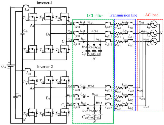
Figure 1.
Circuit topology of the typical 2-group parallel three-phase inverter.
For the parallel three-phase inverter in Figure 1, an inter- and intra-classification model is proposed first. In the following sub-sections, the sub-models of inter-PCC and intra-PCC are given, respectively.
2.1. Sub-Model of the Inter-PCC
For the typical 2-group parallel three-phase inverter in Figure 1, we assume that the AC loads in the phases of a, b, and c are the same, so that the two inverters are equivalent to an AC voltage source with internal resistance [24]. Therefore, Figure 1 can be simplified into the equivalent inter-PCC circuit in Figure 2, where is the output voltage for each group inverter, m = 1, 2; Um and θm represent its amplitude and phase angle, respectively; is the load voltage with the assumption that its phase angle θm is equal to zero in the case of a pure resistive load; ZL is the load impedance; is the current; and is the inter-PCC of the parallel inverter system. And for the individual, Zem is the equivalent output impedance, Zlm is the equal impedance of the transmission line, is the output current, and is the inter-PCC.
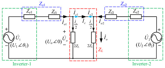
Figure 2.
Equivalent inter-PCC model of Figure 1.
For the equivalent inter-PCC model in Figure 2, we define Zom = Zem + Zlm, and then the steady current can be deduced on the basis of Kirchhoff’s circuit law as follows:
For convenience, it can be considered that Zo1 = Zo2 in the parallel system, that is, Zeq1 = Zeq2, Zlm1 = Zlm2. From (1), the currents and can be represented as follows:
where represents the voltage difference of and .
From (2), we can see that the output current of the individual inverter consists of two parts, that is, the shared current and the inter-PCC. Therefore, the inter-PCC can be expressed as follows:
It should be noted that, the inter-PCC in (3) is produced by the voltage difference , where the individual paralleled inverter is affected by the equivalent output impedance Zem and the equal impedance of the transmission line Zlm, simultaneously. Meanwhile, for the individual inverter in Figure 1, it is difficult to eliminate the correlation for the filter parameters, controller types, and parameters only by the voltage difference [25]. Therefore, an alternative approach is necessary in this paper. From (3), it is a fact that the total inter-PCC of the parallel system can be assigned in accordance with the capacity ratio for the individual inverter. Here, we define km as the capacity proportional coefficient of the m-group inverter, Sm as the capacity of the m-group inverter, km = Sm/∑Si, i = 1, 2. Therefore, the inter-PCC, , for the corresponding m-group inverter can be denoted as follows:
By setting = 0, we can further get:
where SL, PL, and QL are the load capacity, and active and reactive powers, respectively. Obviously, if the inter-PCC of the individual inverter is 0, the load power can be assigned according to the capacity ratio of each parallel inverter; otherwise, if the load power relies on the parallel system, the suppression of the inter-PCC can only be solved indirectly.
2.2. Sub-Model of the Intra-PCC
In the following, we continue to deduce the sub-model of the intra-PCC. Since type of parallel inverter shares a common DC bus, if the problem of the short circuit occurs in the parallel line or in the case of the asymmetric on/off for the corresponding phase power tubes of the individual inverter due to some external disturbances, the equal intra-PCC model can be obtained from Figure 1, where Udc is the DC input voltage, Lsm and C0m are the inductance and capacitance of the main circuit of the inverter, m = 1, 2; Tnm is the power transistor, n = 1, 2, …, 6; ukm is the main circuit output voltage; Lfk1m and Lfk2m are filter inductors; Cfkm is filter capacitance, iLkm and iCkm are the voltage and current; uCkm and iokm are the output voltage and current of the individual inverter, respectively; Rlkm and Llkm are the transmission line resistance and inductance; uskm and isk are the voltage and current of the AC bus, respectively; N is the three-phase midpoint; and Us is the voltage amplitude of the AC side.
In Figure 3, we take Phase A of the two inverters as an example. The current flow is marked by a red dotted line. When the power transistors T11 and T24 at the corresponding link of two inverters are turned on and off asynchronously, the voltage of Point A1 will be higher than that of Point A2, so that a zero-sequence voltage (ZSV) is produced, that is, uz. Furthermore, if uz acts on the impedance of the transmission line, the zero-sequence current iz will be generated, which is the intra-PCC.
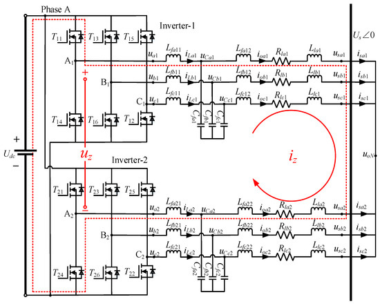
Figure 3.
Equivalent intra-PCC model of Figure 1.
From Figure 3, the current of the 2-group three-phase parallel inverter izm can be denoted as follows:
where iokm represents the output currents of the three-phase m-group parallel inverter, m = 1, 2, and k = a, b, c.
Based on the energy conservation principle, we can see from (5) that the currents iz1 and iz2 have the same value but in the opposite direction for the 2-group parallel inverter. Meanwhile, the generation of izm indicates the fact that the sum of the duty cycles of the three-phase parallel inverter system in Figure 3 cannot be zero. Therefore, we further define dam, dbm, and dcm as the duty cycles for the three-phase abc of the m-group parallel inverter, and the zero-sequence duty cycle (ZSDC) of the m-group parallel inverter as dzm = dam + dbm + dcm, where m = 1, 2.
In Figure 3, since the filtering capacitors Cfam, Cfbm, and Cfcm are not in the PCC path, the ZSV equation for the 2-group three-phase parallel inverter can be deduced on the basis of Kirchhoff’s circuit law as follows:
where Uzm = dzmUdc represents the ZSV of the m-group inverter, m = 1, 2, and k = a, b, c.
Here, Lekm = Lfkm1 + Lfkm2 + Llkm, Lebm = Lfbm1 + Lfbm2 + Llbm, Lecm = Lfcm1 + Lfcm2 + Llcm is defined as the equivalent inductances of the three-phase abc for the m-group parallel inverter, where m = 1, 2. Therefore, by using the Laplace transform, the intra-PCC iz can be deduced by comparing the two inverters in (6) as follows:
which gives the key points concerning the issue of intra-PCC by eliminating ZSV between the corresponding phases.
By combining the inter-PCC expression in (2) and the intra-PCC expression in (7), we can see that they are both related to the corresponding voltage difference for the individual equivalent models in Figure 2 and Figure 3. It also points out the way to solve the inter-PCC and the intra-PCC through voltage compensation at the same time. Specific for the former, since the voltage difference of the inter-PCC in (2) is related to the equivalent output impedance of each paralleled inverter to the AC load side, it is possible to compensate for the inter-phase power difference by the accurate power distribution to ensure the balance of the equivalent output impedance for the two parallel inverters. As a result, the issue of the inter-PCC can be solved. While for the intra-PCC, its idea is based on the voltage difference between the inverter bridges in (7). And the issue of the intra-PCC can be solved by eliminating ZSV indirectly.
2.3. Control Scheme of the Composite SMC
Based on the above analysis, the PCC suppression approaches are designed for the inter-PCC sub-model in (2) and the intra-PCC sub-model in (7), respectively. And the control scheme of the composite SMC is illustrated in Figure 4.
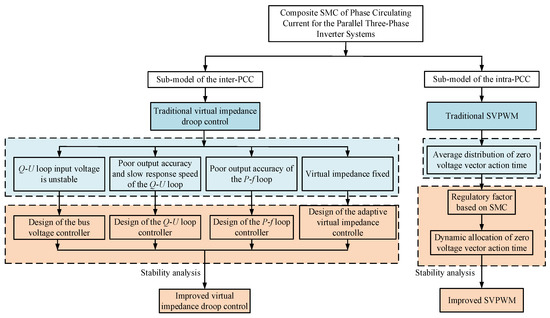
Figure 4.
Control scheme of the composite SMC.
Based on the control scheme of the composite SMC in Figure 4, it can be divided into two parts for analysis and design:
- (1)
- For the sub-model of inter-PCC in (4), the inter-PCC issue can be solved by adjusting the output power distribution accuracy of the paralleled inverter. However, if the traditional virtual impedance droop control is applied in practice, some problems will arise, namely, unstable input voltage of the Q-U loop, low accuracy of the output of the Q-U and P-f loops, slow response speed, and fixed virtual impedance, which affect the inter-PCC of the parallel system. Therefore, this paper focuses on the four aspects of improvement: the bus voltage controller, Q-U loop controller, P-f loop controller, and adaptive virtual impedance controller.
- (2)
- For the sub-model of intra-PCC in (7), the intra-PCC issue can be solved by eliminating the ZSV. For the traditional SVPWM, the ZSV is mainly caused by the average distribution of the action time for the zero voltage vector. Innovatively, this paper will introduce a regulatory factor based on SMC to realize the dynamic distribution of the action time for the zero voltage vector, and an improved SVPWM is proposed.
3. Inter-PCC Suppression Control
Based on the control scheme in Figure 4 and the inter-PCC sub-model in (3), the traditional virtual impedance droop control approach is given, following the improved substitute by combining SMC.
3.1. Traditional Virtual Impedance Droop Control
At present, the virtual impedance droop control is widely used for PCC suppression. It arises on the basis of the droop control approach and the control block diagram, as shown in Figure 5, where UQm and fPm are the output voltage and frequency of the two droop control loops, respectively; δm is the droop loop output angular frequency; udmref and uqmref are the output voltage of the voltage-current double closed-loop control system in the d-q axis, respectively; uvm is the virtual impedance voltage; umref and umref′ are the droop loop output reference voltages before and after subtracting uvm, respectively; and uskm and iskm, are, respectively, the output voltage and current of the m-group parallel inverter.
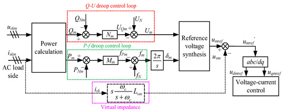
Figure 5.
Control block diagram of the traditional virtual impedance droop control.
The difference between the droop control approach and the virtual impedance droop control lies in the virtual impedance in Figure 5. The traditional droop control approach is to predefine the proportion of the total load capacity for each parallel inverter, which is used for the regulation or compensation of the output for the three-phase inverters. Since the output voltage frequency of the inverter is only determined by the modulation technology, active control is introduced for the power distribution of the loads actively in accordance with their frequency characteristics [26]. Therefore, for the three-phase m-group parallel inverter, m = 1, 2, the relationship between the reactive power and the voltage can be obtained:
where fN, UN, PNm, and QNm are the rated output frequency, voltage, and active and reactive powers for the individual inverter, where m = 1, 2; fm, Um, Pm, and Qm are the actual output frequency, voltage, and active and reactive powers of the m-group parallel inverter; Mm and Nm represent the frequency and voltage droop coefficient of the parallel inverter, respectively, which are inversely proportional to the capacity of the individual inverter [27].
For (8), if the three-phase parallel inverter system works steadily, the output frequency of the individual inverter can be equalized by using the same modulation technology [28]. And the active power of the loads can be distributed in accordance with the droop coefficient Mm in (8). Meanwhile, due to the difference between the output impedance and line transmission impedance, it is impossible to guarantee that the output voltage of the individual inverter is equal, and the load reactive power cannot be accurately distributed in accordance with the voltage droop coefficient Nm in (8). However, it should be noted that the traditional droop control relies on the inductive resistance of the transmission line, that is, if the resistance value is much larger than the inductive impedance, oscillations will occur inevitably, which leads to an unstable system.
While for the virtual impedance droop control, the power transmission with added virtual impedance is shown in Figure 6, it can be obtained from Figure 5, where and are, respectively, the output voltage and current of the inverter, where m = 1, 2, and θm is the voltage difference angle; Zom is the equivalent output impedance of the inverter; jXem is the total equivalent output impedance for the m-group parallel inverter; Xvm is the virtual reactance; Lvm is the virtual inductance; Sm is the output power of the individual inverter to the AC bus; Pm and Qm represent the active and reactive components, respectively; and Zlm is the transmission line impedance.
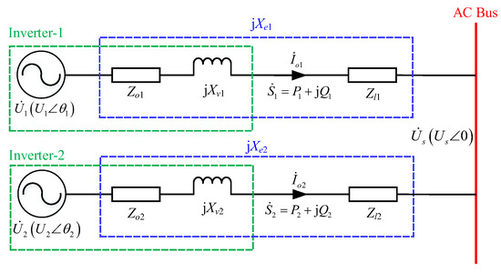
Figure 6.
Power transmission of the traditional virtual impedance droop control.
For the virtual impedance droop control in Figure 6, there is a series connection between the virtual impedance and the actual output impedance for the three-phase parallel inverter system [29]. In other words, by subtracting an appropriate and fixed value of the impedance voltage drop from the output voltage of the Q-U droop control loop, the resistive effect of the transmission line can be removed.
Based on the virtual impedance droop control and Figure 6, the output power for the three-phase m-group parallel inverter system to the AC bus can be expressed as follows:
Considering the added virtual impedances, we substitute (8) into (9), yielding the reactive power as follows:
In order to realize the distribution of the reactive power for the loads by adjusting the voltage droop coefficient Nm in (8), that is, N1Q1 = N2Q2, the condition U1 = U2 needs to be satisfied. Therefore, from (10), the voltage difference ΔU can be calculated as follows:
In order to realize the PCC suppression by using the virtual impedance droop control, the following conditions need to be satisfied by setting ΔU = 0 in (11):
- The total equivalent output inductance Xem needs to be proportional to Nm.
- The phase angle of the output voltage θm is the same for the contained parallel inverters.
3.2. Improved Virtual Impedance Droop Control
Based on the above virtual impedance droop control in Figure 5, this paper improves its control performance by using SMC. The control diagram is illustrated in Figure 7, where Us′ and fs′ are the voltage amplitude and frequency of the controller output, respectively; isa and ioam are the currents of the A-phase inverter output and of the grid, respectively; and RMS represents the root mean square measurement.
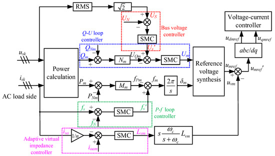
Figure 7.
Control block diagram of the improved virtual impedance droop control.
Compared with the traditional virtual impedance droop control in Figure 5, we can see that the improvements of the proposed approach in this paper lie in the design of the four parts, that is, the bus voltage controller, Q-U loop controller, P-f loop controller, and adaptive virtual impedance controller, where SMC is adopted. Specifically, the bus voltage controller is for the control of Us to follow the rated value UN stably; the Q-U loop controller is to reduce the impact of the output impedance and transmission line impedance on the reactive power distribution, as well as to improve the response speed of the system; the P-f loop controller is to regulate the voltage frequency fs of the AC bus in accordance with the rated frequency fN; and the adaptive virtual impedance controller is designed to overcome the possible external disturbances and parameter perturbations during the transmission process.
In the following, SMC is utilized for the controller design for the bus voltage, Q-U loop, P-f loop, and adaptive virtual impedance, respectively.
3.2.1. Design of the Bus Voltage Controller
From Figure 7, the function of the bus voltage controller is to drive the bus voltage Us to follow the rated value UN stably. Therefore, we define the deviation variable xU as follows:
Based on the principle of SMC, the design of a SMC controller generally includes a sliding surface and a robust control law [30]. Therefore, from (12), the commonly used linear sliding mode controller is adopted for the design of the sliding surface SU:
where cU1 > 0 is a proportional adjustment parameter for changing the response speed; cU2 > 0 is the coefficient of an integral term, which is used to eliminate the static error of the system.
In this paper, the exponential reaching law is adopted for the design of the robust control law, that is, it has:
where the design parameters εU > 0 and kU > 0 can be deduced by the existence condition of SMC, that is, SU = 0. And the convergence time tU can also be obtained as follows:
where SU(0) is the initial value of the sliding variable SU.
From (15), we can see that the convergence time tU is determined by the design parameters εU, kU in (14) and the initial point SU(0) at the same time. Obviously, the bigger the parameters εU and kU are, the smaller the convergence time tU is, and the larger SU(0) is, the bigger the convergence time tU is. In Figure 8, the relationship between the parameters εU, kU, and SU(0) and the convergence time tU is shown in phase plane SU–.
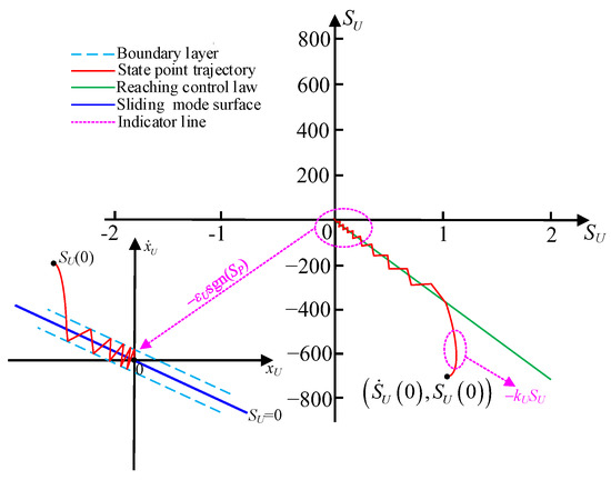
Figure 8.
Relationship of εU, kU, SU(0) and the convergence time tU in the phase plane SU–.
From Figure 8, since the design parameters εU and kU in (14) determine the convergence time of the system to the equilibrium point SU = 0, that is, if SU(0) is initially big, it deviates far from SU = 0, and the term −kUSU in (15) will accelerate the system convergence, while as the system reaches around SU = 0, the term of −kUSU becomes very small. At this time, −εUsgn(SU) ensures that the voltage state switches up and down continuously along SU = 0 at a constant speed εU, which ensures that it reaches a steady-state within a finite time. However, it should be noted that, since εU determines the ultimate speed at which the voltage state switches at SU = 0, the value of εU also affects the chattering situation of the SMC system, and this item should be appropriately small. Therefore, the selection of kU and εU should be appropriately small; otherwise, it will affect the convergence and stability of the system. Furthermore, the parameter selection of other controllers designed in this paper can also refer to the above analysis.
In order to analyze the stability of the bus voltage control system using SMC, we chose the Lyapunov equation VU = 0.5SU2. By substituting (14), it yields:
which indicates the finite-time convergence of the bus voltage control system.
3.2.2. Design of the Q-U Loop Controller
For the Q-U loop controller, its function is to reduce the impact of the output impedance and transmission line impedance on the reactive power distribution, as well as to improve the response speed of the system. In other words, the output value Us′ needs to track the reference value of the Q-U loop UQm. Therefore, we define an error variable xE as follows:
Similar to the SMC design for the voltage control system in (12)–(14), the sliding surface SE and the robust control law are designed as follows:
where the design parameters are cE1 > 0, cE2 > 0, εE > 0, and kE > 0.
Furthermore, the Lyapunov equation VE = 0.5SE2 is constructed to verify the stability of the Q-U loop control system. Taking the derivative of VE and substituting (19) into it, we can get:
which also indicates the finite-time convergence of the Q-U loop.
Similar to the analysis of the convergence characteristics in Figure 8, we can get the trajectory in phase plane SE– in Figure 9, where the red solid line represents the improved reaching law in (20), and the blue broken line represents the traditional exponential reaching law similar to (14).
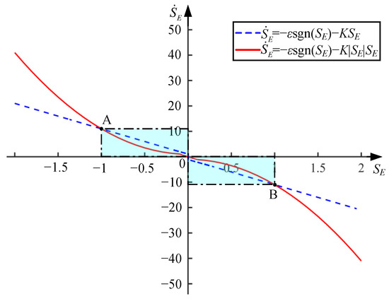
Figure 9.
Comparison of the control law in phase plane SE–.
In Figure 9, the trajectories at Point A (−1, 11) and Point B (1, −11) correspond to the intersection of two different control laws, where the design parameters in (18) and (19) are selected as εE = 1 and kE = 10. It indicates that, when the initial voltage state (SE(0), (0)) exceeds the hidden area enclosed by the state curves of Point A and Point B, the response speed of the improved approach law will be faster than that of the traditional approach law, which corresponds precisely to the initial characteristics of the Q-U loop. Furthermore, from (8), the output voltage amplitude of the parallel inverter system is around 311 V, that is, the amplitude of Us′ will be much larger than the value of the term Nm(Qm − QNm), which will cause the initial voltage state SE(0) of the Q-U loop output to deviate significantly from the origin. Due to the improved approaching law in (20), the voltage state will have a prompt and high approaching speed in an instant, that is, (0) will suddenly increase. It has been proven that the improvement is more suitable for designing Q-U control loop output voltages with rapid response. However, it is worth noting that such improvements, to some extent, sacrifice the robustness of SMC near the origin, so it needs to be judged based on the actual needs of different controllers.
Finally, by substituting the control parameters from (18) and (19) into (8) and using the Laplace transform, the Q-U loop control system can be rewritten in the frequency domain as follows:
3.2.3. Design of the P-f Loop Controller
For the P-f loop controller, it is to regulate the voltage frequency fs of the AC bus in accordance with the rated frequency fN. Therefore, we define an error variable xf as follows:
Similar to the SMC design for the voltage control system in (12)–(14), the sliding surface Sf and the robust control law uf are designed as follows:
where the design parameters are cf1 > 0, cf2 > 0, εf > 0, and kf > 0.
Similar to the Laplace transform in (21), the P-f loop control system can be rewritten in the frequency domain as follows:
The stability analysis is the same as in (14); it is ignored here. By combining (21) and (25), if the P-f loop control system works steadily, the input of the individual inverter’s integrators in (21) and (25) approximates zero [31]. Therefore, it has:
where ΔPm = PmPNm, ΔQm = QmQNm, Δfs = fsfN, and ΔUs = UsUN, where m = 1, 2.
In order to guarantee the parallel inverter system works stably, it is only necessary to set the control parameters cf1, cf2, cE1, and cE2 of the individual inverter in (26) as the same. Therefore, it has:
which ensures the precise distribution of load power in parallel inverter systems.
From Figure 7, it is worth noting that the voltage error of RMS, defined as ΔUsm′, can affect the accuracy of load reactive power allocation. Therefore, the reactive power error ΔQm′ can be deduced as follows:
Specifically, for the 2-group parallel three-phase inverter system, the reactive power error eQ produced by RMS error ΔUs′ = M1ΔUs1′ − M2ΔUs2′ can be expressed as follows:
3.2.4. Design of the Adaptive Virtual Impedance Controller
For the adaptive virtual impedance controller, its function is to overcome the external disturbances and parameter perturbations during the transmission process incurred by the inductive reactance Xvm. In this paper, an adaptive Xvm regulator is designed based on the difference between the output current iokm for the single-phase inverter and grid current isk, where m = 1, 2, and k = a, b, c. Therefore, we define an error variable xc as follows:
Similar to the SMC design for the voltage control system in (12)–(14), the sliding surface Sc and the robust control law uc are designed as follows:
where the design parameters are cc1 > 0, cc2 > 0, εc > 0, and kc > 0.
In practice, when the virtual inductance Xvm is adjusted to an appropriate value, the reactance component in the equivalent line impedance can guarantee the ideal droop control at the expense of aggravating the output voltage drop of the inverter system, causing the offset of the AC bus voltage Us. Meanwhile, from (31), the inherent chattering issue of SMC also affects the reference voltage Us′. Therefore, it is necessary to limit the virtual impedance value of the controller output based on the voltage drop generated by Xvm. Furthermore, from Figure 6, if the system works steady, the output voltage of the inverter system is equal to the rated reference voltage, that is, Uom = UN. Therefore, the vector of the voltage drop caused by Xvm can be illustrated in Figure 10 [32], where UQm is the output voltage of the Q-U loop in Figure 7; Umref′ is the given reference voltage of the droop loop after adding Xvm; Uvm is the voltage drop generated on Xvm; and ψ is the phase difference between Urefm and UQm after adding Xvm.
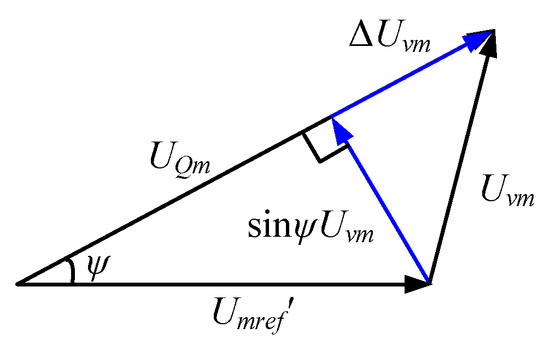
Figure 10.
The vector analysis of the voltage drop caused by Xvm.
In Figure 10, since Uvm can be decomposed into ΔUvm and sinψUvm along the direction of UQm, Uvm ≈ ΔUvm holds approximately due to the small value of ψ. Since Xvm can incur an inductive equivalent impedance of the transmission line, to simplify the analysis, Xvm can only affect the output reactive power Qm of the system. Therefore, from (9), it has:
When the inverter system works steadily, UQm equals the actual output voltage Um of the inverter on the basis of SMC. By combining (33) and the Q-U loop control in (21), the Q-U loop control system after adding Xvm can be rewritten by using the Laplace transform as:
where Nvm = Xvm/UQm is the droop voltage coefficient.
Due to the droop limit in (34), the maximum output voltage distortion rate can be set based on its output characteristics γ%, and the maximum output reactive power is Qmax [33]. Therefore, it has:
By substituting (34) into (35), the upper limit of Xvm can be obtained as follows:
3.3. Stability Analysis of the Improved Virtual Impedance Droop Control
In the following, the stability of the improved virtual impedance droop control by using SMC is investigated, and the analysis approach of the small signal is utilized.
From (9), the average output power of the inverter system can be expressed by the first-order low-pass filter:
where ωc is the cutoff frequency of the first-order low-pass filter.
By introducing disturbance values to each output signal of the parallel system in (37), we can get:
where, , , , and represent disturbance values of Um, θm, Pm, and Qm, respectively.
By combining (37) and (38), the small signal disturbance can be obtained as follows:
Based on the perturbation theory of the small signal [34] and (8), we can further get:
where represents the disturbance value of fm.
Furthermore, by substituting (21) and (25) into (40), the small-signal expression can be obtained as follows:
From Figure 7, the relationship between the frequency disturbance of the output voltage and the phase disturbance can be expressed as follows:
By combining (40)–(42), the small signal perturbation equation of and can be obtained as follows:
which can be further rewritten as follows:
where a, b, c, d, and e can be denoted as follows:
By solving (44), the trajectory of the system can be illustrated in Figure 11, where λ1–λ4 represents the typical root, and the arrow direction represents the movement direction of the characteristic root with the increase in parameters.
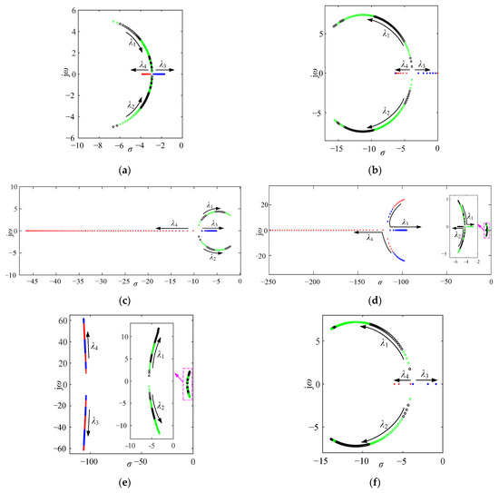
Figure 11.
Root locus of the improved virtual impedance droop control: (a) 0 ≤ cf1 ≤ 10, (b) 0 ≤ cE2 ≤ 100, (c) 0 ≤ cf2 ≤ 100, (d) 0 ≤ cE1 ≤ 10, (e) 1 × 10⁻⁶ ≤ Mm ≤ 1 × 10⁻⁴, and (f) 1 × 10⁻⁴ ≤ Nm ≤ 1 × 10⁻².
From Figure 11, we can see that the root locus is located on the left half of the complex plane, which validates the system’s stability by using the improved virtual impedance droop control in Figure 7.
Specifically, Figure 11a corresponds to the system root trajectory, where only the proportional parameter cf1 changes. As cf2 increases, conjugated complex roots λ1 and λ2 quickly move towards the real and imaginary axes, the oscillation frequency and damping of the system begin to decrease, and the response speed and stability are improved. The real roots λ3 and λ4 move left and right at a similar speed, but have less impact on the system. In conclusion, the larger cf2 is, the more stable the system is.
From Figure 11b, as cE2 increases, the conjugated complex roots λ1 and λ2 move away from the real and imaginary axes, and the oscillation frequency and damping of the system rise rapidly, resulting in a slow response speed and poor stability. Although the dispersed motion of real roots λ3 and λ4 exhibits a gradual increase in damping, its impact on the system is relatively weak. In conclusion, the smaller the cE2 and Nm are, the faster the system’s response is.
Figure 11c illustrates the root trajectory with the variation of the integral term parameter cf2. With the increase in cf2, conjugated complex roots λ1 and λ2 move away from the real axis and towards the imaginary axis, the oscillation frequency of the system slightly increases, and the damping is relatively small; the real root λ4 moves to the left along the real axis at a speed much quicker than that of λ3, resulting in an increasing damping of the dominant system. In other words, the parameter cf2 is helpful for the system’s stability.
In Figure 11d, it shows the root trajectory in the case of the proportional parameter cE1 varying. We can see that, the conjugate complex roots λ3 and λ4 move towards the real axis, and when they are the real roots, λ4 moves to the left at a faster speed than that of λ3, and the damping of the system increases while the oscillation frequency decreases. λ1 and λ2 move towards the real axis at similar speeds, but the impact is relatively weak. In other words, the parameter cE1 is suggested to be smaller so that a fast response can be achieved.
In Figure 11e, it shows that the root trajectory varies with the power droop coefficient Mm. With the increase in Mm, λ1–λ4 move away from the real axis, which incurs a significant increase in the system oscillation frequency. In other words, the parameter Mm is suggested to be smaller to guarantee the better stability of the system.
4. Intra-PCC Suppression Control
In the following, the suppression of the intra-PCC will be investigated based on the control scheme in Figure 4. Based on the intra-PCC sub-model in (7), PCC suppression relies on eliminating ZSV between the corresponding phases. For SVPWM, since the zero voltage vector does not affect the synthesis of modulated signals by other non-zero vectors, a regulation factor km is introduced to control ZSDC for (6) [35]. Therefore, for the parallel three-phase inverter system in Figure 1, the signal in a modulation sector with regulation factor km can be illustrated in Figure 12, where Tc is a modulation time; dam, dbm, and dcm represent the duty cycle of the switch signal on the three-phase bridge arm of the inverter; d0m represents the action time of the zero voltage vector; d1m and d2m represent the action time of non-zero voltage vectors with d0m + d1m + d2m = 1; and TSam, TSbm, and TScm represent the switching time of the synthesized vector on the three-phase bridge.
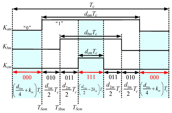
Figure 12.
Signal in a modulation sector with the regulation factor km.
Assume that d0mTc = t0m, d1mTc = t1m, and d2mTc = t2m. From Figure 12, the action time of the zero vector t0m = Tc − t1m − t2m, and the duty cycle of the switch signal on the three-phase bridge arm dam, dbm, and dcm can be given as follows:
By combining (5) and (46), ZSDC dzm can be expressed as follows:
Since t0m > 0, the variation range of km in (47) is [−d0m/4, d0m/4]. Due to the regulation factor km, the adjusted action time of the three-phase bridges TSam′, TSbm′, and TScm′ can be written as follows:
By substituting (48) into (7), the intra-PCC can be rewritten as follows:
In order to suppress the intra-PCC in (49), it is critical to determine the regulation factor km. A SMC-based approach is designed in Figure 13, where L is an amplitude limiter, which can force the regulation factor km to vary within [−d0m/4, d0m/4].

Figure 13.
Control diagram of the proposed SMC-based approach.
Since the desired intra-PCC is zero, the state xz can be denoted as follows:
Similar to the SMC design for the voltage control system in (12)–(14), the sliding surface Sz and the robust control law uz are designed as follows:
where the design parameters are cz1 > 0, cz2 > 0, εz > 0, and kz > 0.
5. Simulation and Experiment
For the 2-group parallel three-phase inverter system in Figure 1, the composite control scheme for simulation and experiment is shown in Figure 14. The circuit parameters are shown in Table 1, where m = 1, 2. For the transmission line, its impedance Zlm = 0.101 + j0.231 Ω/km is the actual value of a three-core cable [36], the reference cross-sectional area is 185 mm2, and the length of the transmission line is 2 km.
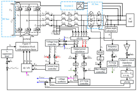
Figure 14.
Composite control scheme of a 2-group parallel three-phase inverter system.

Table 1.
Circuit parameters of the 2-group parallel three-phase inverter.
In order to validate the effectiveness of the parallel inter-controllers and intra-controllers designed in Section 3.2 and Section 4, the system performance is compared with the traditional virtual impedance droop control introduced in Section 3.1, and the design parameters of the two strategies are given in Table 2 and Table 3, respectively. In Table 3, the subscripts “u” and “i” represent the PI parameters of the voltage outer loop and the current inner loop of the traditional strategy, respectively, and “d” and “q” represent the control parameters corresponding to the d-q axis, respectively. The simulation sampling period is set to 1 μs. For distinguishing the two approaches in the following, we use “VI” and “CS” located in the subscript of the variables to denote the corresponding values under the traditional virtual impedance droop control in Section 3.1 and the proposed composite control in Figure 14.

Table 2.
Design parameters of the inter-controllers and intra-controllers.

Table 3.
Design parameters of the traditional virtual impedance droop controller.
5.1. Simulation Results
In simulation, we choose two typical working conditions of the three-phase parallel inverter system to validate the proposed composite control scheme in Figure 14, that is, the rated working case and the working case with disturbances.
5.1.1. Case 1: Rated Working Case
In this case, the working condition is described by the following phases:
- (1)
- Phase 1: Set the load power to be consistent with the rated power at t = 0.
- (2)
- Phase 2: Increase the total load power to PL = 8 kW and QL = 800 var at t = 0.15 s.
- (3)
- Phase 3: Decrease the total load power to PL = 4 kW and QL = 400 var at t = 0.3 s.
For the 2-group parallel three-phase inverter system in Figure 1, the comparative simulation results are shown in Figure 15. Due to the parallel structure and similar performances, Table 4 and Figure 16 concerning the corresponding error integrals only list the comparative data of Inverter-1 for reference.
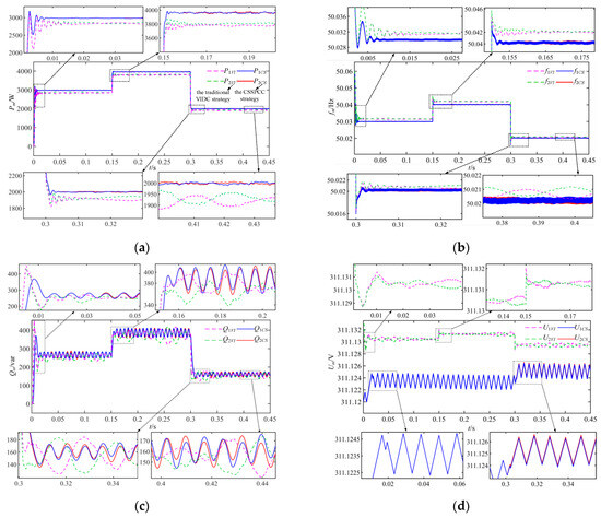
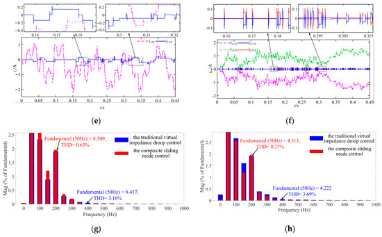
Figure 15.
Comparative simulation results in rated working conditions: (a) output active power Pm, (b) P-f loop output frequency fm, (c) output reactive power Qm, (d) Q-U loop output voltage amplitude Um, (e) inter-PCC ic, (f) intra-PCC iz, (g) harmonic analysis of ia in Phase 2, and (h) harmonic analysis of ia in Phase 3.

Table 4.
Comparative simulation results of Inverter-1 in the rated working condition.
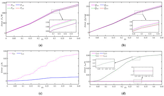
Figure 16.
Comparative integral errors of Inverter-1 in the rated working condition: (a) integral error of Pm, (b) integral error of Qm, (c) integral error of ic, and (d) integral error of izm.
In Figure 15a, the active power output Pm of the 2-group three-phase inverter system is given, where m = 1, 2. Taking inverter-1 as an example in Table 4, we can see that the dynamic and static control performances of the proposed composite control are better than those under the traditional virtual impedance droop control. For example, the initial convergence time of P1CS is reduced by 66.7% while P1VI is only 0.012 s; the overshoot of P1CS is within 6.6% and reduced by 21.7% in comparison to P1VI, so that the stability of the output active power can be guaranteed. When the load power changes, the average response time of P1CS is reduced by nearly 58.8% with comparison to P1VI, due to the use of SMC. The mean steady-state error of P1CS is only 19.7 W, which is nearly 84.8% lower than P1VI.
Figure 15b shows the output frequency fm of the P-f loop, and the average response time and steady-state error of the f1CS are reduced by 54.6% and 9.1%, respectively, compared to f1VI, due to control relationships in Section 3.2.3, and the improved P-f droop control loop can effectively improve the accuracy of output frequency by the designed SMC adjustment. Figure 15c shows that the output reactive power Qm and Q1CS can stabilize in 0.015 s; the maximum overshoot is 39.4%, compared to Q1VI. It is due to the stability control of the output voltage U1 of the Q-U loop in Section 3.2.2. We can see at t = 0.15 s, U1VI suddenly increases along QL in Figure 15d, Q1VI has large fluctuations, and U1CS remains stable, which is due to the design of the SMC controller with bus voltage in Section 3.2.1, stabilizing the bus voltage to reduce the fluctuation of the Q-U loop input reference voltage amplitude. While at t = 0.3 s, U1VI experiences a sudden decrease due to the reduction in QL and Q1VI fluctuates greatly. Meanwhile, due to the fast response of SMC, the average response time of U1CS has been reduced by 33.3%, which is in accordance with Figure 15a. In Figure 15e,f, the inter-PCC ic and the intra-PCC iz are shown, respectively. Taking the inverter-1 as an example, the inter-PCC icCS is only 0.191A and is 80.6% less than that of icVI, while the intra-PCC iz1CS is only 0.093 A and is 88.1% less than iz1VI. And the harmonic content of ia in Phase 2 and Phase 3 under the composite SMC strategy is 20% and 10% of that under the traditional virtual impedance droop control strategy, respectively. Therefore, the proposed composite control scheme in Figure 14 has been proven effective.
5.1.2. Case 2: Working Conditions with Disturbances
In this case, we take the disturbance of the transmission line as an example to test the proposed composite control scheme in Figure 14. In practice, this kind of disturbance is very common and is characterized by unmatched uncertainty in the sense of SMC [38]. Specifically, the working condition is described by the following phases:
- (1)
- Phase 1: The transmission line Zlm = 0.101 + j0.231 Ω/km at t = 0.
- (2)
- Phase 2: Zlm decreases to 0.051 + j0.116 Ω/km at t = 0.15 s.
- (3)
- Phase 3: Zlm increases to 0.202 + j0.462 Ω/km at t = 0.3 s.
For the 2-group three-phase inverter system in Figure 1, the comparative simulation results are shown in Figure 17. Similar to Table 4, Table 5 only shows the comparative data of Inverter-1 for reference.
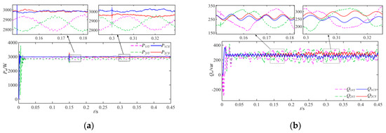
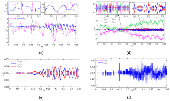
Figure 17.
Comparative simulation results in the working condition with disturbances: (a) output active power Pm, (b) output reactive power Qm, (c) inter-PCC ic, (d) intra-PCC iz, (e) virtual inductive Xvm, and (f) regulation factor km.

Table 5.
Comparative simulation results of Inverter-1 in the disturbing working condition.
In Figure 17a, the active Pm is given for the 2-group three-phase inverter system, where m = 1, 2. Taking inverter-1 as an example in Table 5, since the imbalance of the transmission lines exists, P1VI and P1CS fluctuate at the same time. By comparing Table 4 and Table 5, we can see that, the maximum error of P1VI is 225.324 W, and the mean steady-state error increases by 13.7% due to the disturbance of the transmission line. While the maximum error of P1CS is only about 1/5 of P1VI and its steady-state error only increases by 11.9%, the stable time is 66.7% lower than P1VI. Figure 17b shows the reactive power Qm. In the case of the traditional virtual impedance droop control, the maximum error of Q1VI is 132.785 var, while in the case of proposed composite control, the maximum error of Q1CS is reduced by 51.7%. Figure 17c,d show the inter-PCC ic and the intra-PCC izm. Due to the adaptive adjustment of the virtual inductance Xv1 and the regulation factor k1, the suppression of inter-PCC ic and intra-PCC iz1 can be realized, respectively, and Figure 17e,f show Xv1 and k1 for reference.
5.2. Experiment Results
In the following, the proposed composite control scheme in Figure 14 is tested on the experimental platform of dSPACE1006 (dSPACE Inc., Konstanz, Germany), shown in Figure 18. The traditional virtual impedance droop control is also adopted for comparison with the proposed composite control in this paper. The relevant parameters of the experimental test bench in Figure 18 are consistent with the simulation process, as shown in Table 1, and the design parameters of the controllers can be referred to in Table 2 and Table 3. The experiment results are in Figure 19 and Table 6.
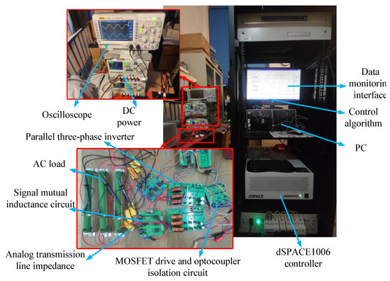
Figure 18.
The experimental platform of dSPACE1006.
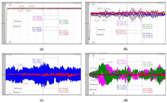
Figure 19.
Comparative experimental results: (a) active power Pm, (b) reactive power Qm, (c) inter-PCC ic, and (d) intra-PCC iz.

Table 6.
Experimental comparisons of Inverter-1 and Inverter-2.
In Figure 19a, the experiment results of the active power Pm are given for the 2-group parallel three-phase inverter system, where m = 1, 2. For the invereter-1 and inverter-2, the proposed composite control scheme in Figure 14 can guarantee the active power P1CS and P2CS are stable within 0.071 s. And from Table 6, the amplitude errors of P1CS and P2CS decrease by 28.3% and 28.4% compared to P1VI and P2VI in the case of the traditional virtual impedance droop control; while the mean steady-state error of P1CS and P2CS is 21.947 W and 22.253 W, which are decreased by 84.1% and 83.9% compared to P1VI and P2VI. In Figure 19b, it shows the reactive power QmCS. And from Table 6, the amplitude errors of Q1CS and Q2CS for the two inverters are only 54.045 var and 54.704 var, which are 66.7% and 64.3% lower than the Q1VI and Q2VI under the traditional approach. Figure 19c,d show the inter-PCC ic and the intra-PCC iz. In the case of the traditional approach, both the inter-PCC and the intra-PCC contain high-frequency oscillations, which are dangerous in practice and can be prevented; otherwise, they have serious side effects on the power quality and conversion efficiency of the power grid. While under the control of the proposed composite control scheme in Figure 14, the steady-state error of icCS is 0.216 A, which is 82.4% lower than icVI, the steady-state errors of iz1CS and iz2CS are 0.123 A and 0.127 A, which are 86.9% and 86.8% lower than iz1VI and iz2VI, respectively. Therefore, it reconfirms the superiority of the proposed approach.
6. Conclusions
In this paper, a composite SMC approach is proposed for the parallel three-phase inverter system to solve the issue of PCC suppression. Differing from traditional research, which only considers the intra-PCC or the inter-PCC, we investigate both at the same time and propose an inter- and intra-classification model. For the intra-PCC, based on the analysis of the traditional virtual impedance droop control, novel SMC controllers are designed with the focus of robustness and fast response for the coupled control, including bus voltage, Q-U loop, P-f loop, and the virtual induced reactance. As a result, the intra-PCC is significantly suppressed, and the output accuracy and response speed of the system are improved compared with the traditional virtual impedance droop control. Innovatively, a regulation factor is introduced into SVPWM, so that the intra-PCC can be relieved by eliminating the zero-sequence voltage compared with the traditional SVPWM. For future research, we will focus on how to improve control performance by using other types of SMC, which can be of significance in theory and practice.
Author Contributions
Conceptualization, Y.W., W.Z. and F.H.; methodology, W.Z.; software, F.H. and W.Z.; validation, Y.W., F.H. and R.Y.; formal analysis, W.Z. and Y.W.; investigation, F.H.; resources, R.Y.; data curation, Y.W.; writing—original draft preparation, Y.W. and F.H.; writing—review and editing, Y.W. and F.H.; visualization, W.Z.; supervision, Y.W. and F.H.; project administration, Y.W.; funding acquisition, Y.W. and F.H. All authors have read and agreed to the published version of the manuscript.
Funding
This research was funded by the National Natural Science Foundation of China (grant numbers: 51307035 and 62073095).
Data Availability Statement
Data are contained within the article.
Conflicts of Interest
The authors declare no conflicts of interest.
References
- Hu, J.; Yuan, H.; Yuan, X. Modeling of Dfig-Based WTS for Small-Signal Stability Analysis in DVC Timescale in Power Electronized Power Systems. IEEE Trans. Energy Convers. 2017, 32, 1151–1165. [Google Scholar] [CrossRef]
- Cano, T.C.; Castro, I.; Rodriguez, A.; Lamar, D.G.; Khalil, Y.F.; Albiol-Tendillo, L.; Kshirsagar, P. Future of Electrical Aircraft Energy Power Systems: An Architecture Review. IEEE Trans. Transp. Electrif. 2021, 7, 1915–1929. [Google Scholar] [CrossRef]
- Jain, H.; Mather, A.; Jain, A.K.; Baldwin, S.F. Grid-Supportive Loads—A New Approach to Increasing Renewable Energy in Power Systems. IEEE Trans. Smart Grid 2022, 13, 2959–2972. [Google Scholar] [CrossRef]
- Ma, D.; Chen, W.; Shu, L.; Qu, X.; Hou, K. A Mmc-Based Multiport Power Electronic Transformer with Shared Medium-Frequency Transformer. IEEE Trans. Circuits Syst. II-Express Briefs 2020, 68, 727–731. [Google Scholar] [CrossRef]
- Qanbari, T.; Tousi, B. Single-Source Three-Phase Multilevel Inverter Assembled by Three-Phase Two-Level Inverter and Two Single-Phase Cascaded H-Bridge Inverters. IEEE Trans. Power Electron. 2021, 36, 5204–5212. [Google Scholar] [CrossRef]
- Alenius, H.; Roinila, T.; Luhtala, R.; Messo, T.; Burstein, A.; de Jong, E.; Fabian, A. Hardware-in-the-Loop Methods for Stability Analysis of Multiple Parallel Inverters in Three-Phase AC Systems. IEEE J. Emerg. Sel. Top. Power Electron. 2021, 9, 7149–7158. [Google Scholar] [CrossRef]
- Fu, Y.; Li, Y.; Huang, Y.; Lu, X.; Zou, K.; Chen, C.; Bai, H. Imbalanced Load Regulation Based on Virtual Resistance of a Three-Phase Four-Wire Inverter for EV Vehicle-to-Home Applications. IEEE Trans. Transp. Electrif. 2019, 5, 162–173. [Google Scholar] [CrossRef]
- Hu, X.; Tseng, K.J. Integration of Multiple Modularized Distributed Energy Resource Devices into Ac Grid of Buildings: Issue of Active Power Circulation. IEEE Trans. Ind. Electron. 2014, 61, 6118–6127. [Google Scholar] [CrossRef]
- Zhang, C.; Wang, Z.; Xing, X.; Li, X.; Liu, X. Modeling and Suppression of Circulating Currents Among Parallel Single-Phase Three-Level Grid-Tied Inverters. IEEE Trans. Ind. Electron. 2022, 69, 12967–12979. [Google Scholar] [CrossRef]
- Fan, B.; Li, Q.; Wang, W.; Yao, G.; Ma, H.; Zeng, X.; Guerrero, J. A Novel Droop Control Strategy of Reactive Power Sharing Based on Adaptive Virtual Impedance in Microgrids. IEEE Trans. Ind. Electron. 2022, 69, 11335–11347. [Google Scholar] [CrossRef]
- Guo, C.; Wu, S.; Yang, S.; Hu, J. Overcurrent Suppression Control for Hybrid LCC/VSC Cascaded HVDC System Based on Fuzzy Clustering and Identification Approach. IEEE Trans. Power Deliv. 2022, 37, 1745–1753. [Google Scholar] [CrossRef]
- Si, Y.; Wang, R.; Zhang, S. Fault Diagnosis Based on Attention Collaborative LSTM Networks for NPC Three-Level Inverters. IEEE Trans. Instrum. Meas. 2022, 71, 3512416. [Google Scholar] [CrossRef]
- Judewicz, M.G.; González, S.A.; Fischer, J.R.; Martínez, J.F.; Carrica, D.O. Inverter-Side Current Control of Grid-Connected Voltage Source Inverters with LCL Filter Based on Generalized Predictive Control. IEEE J. Emerg. Sel. Top. Power Electron. 2018, 6, 1732–1743. [Google Scholar] [CrossRef]
- Wei, B.; Marzàbal, A.; Ruiz, R.; Guerrero, J.M.; Vasquez, J.C. DAVIC: A New Distributed Adaptive Virtual Impedance Control for Parallel-Connected Voltage Source Inverters in Modular UPS System. IEEE Trans. Power Electron. 2019, 34, 5953–5968. [Google Scholar] [CrossRef]
- Yeam, T.; Hu, H.; Ge, Y. Design of Sliding-Mode Speed Controller with Active Damping Control for Single-Inverter Dual-Pmsm Drive Systems. IEEE Trans. Power Electron. 2021, 36, 5794–5801. [Google Scholar] [CrossRef]
- Yang, X.; Hu, H.; Ge, Y.; Aatif, S.; He, Z.; Gao, S. An Improved Droop Control Strategy for VSC-Based Mvdc Traction Power Supply System. IEEE Trans. Ind. Appl. 2018, 54, 5173–5186. [Google Scholar] [CrossRef]
- Liu, J.; Sun, X.; Ren, B.; Zhang, Q. Dynamic Circulating Current Suppression Method for Multiple Hybrid Power Parallel Grid-Connected Inverters with Model Reference Adaptive System. IEEE Trans. Ind. Electron. 2022, 69, 4364–4375. [Google Scholar] [CrossRef]
- Zhang, M.; Song, B.; Wang, J. Circulating Current Control Strategy Based on Equivalent Feeder for Parallel Inverters in Islanded Microgrid. IEEE Trans. Power Syst. 2019, 34, 595–605. [Google Scholar] [CrossRef]
- Zhou, S.; Liu, K.; Wu, J.; Li, K.; Huang, C.; Zhang, D. Differential-Mode Circulating Current Suppression for Paralleled Inverters Fed PMSM Drives Considering Dead Time Compensation. IEEE Trans. Power Electron. 2023, 38, 8742–8753. [Google Scholar] [CrossRef]
- Choi, H.; Lee, K. Circulating Current Reduction for Parallel-Connected Modular Inverters Based on Suppression of Common-Mode Voltage. IEEE Trans. Power Electron. 2023, 38, 11091–11101. [Google Scholar] [CrossRef]
- Yang, Y.; Wai, R. Design of Adaptive Fuzzy-Neural-Network-Imitating Sliding-Mode Control for Parallel-Inverter System in Islanded Micro-Grid. IEEE Access 2021, 9, 56376–56396. [Google Scholar] [CrossRef]
- Yang, X.; Li, Z.; Zheng, T.Q.; You, X.; Kobrle, P. Virtual Impedance Sliding Mode Control-Based MMC Circulating Current Suppressing Strategy. IEEE Access 2021, 7, 26229–26240. [Google Scholar] [CrossRef]
- Zorig, A.; Belkheiri, M.; Barkat, S.; Rabhi, A.; Blaabjerg, F. Sliding Mode Control and Modified SVM for Suppressing Circulating Currents in Parallel-Connected Inverters. Electr. Power Compon. Syst. 2018, 46, 1061–1071. [Google Scholar] [CrossRef]
- Chen, J.; Sha, D.; Zhang, J.; Liao, X. A Variable Switching Frequency Space Vector Modulation Technique for Zero-Voltage Switching in Two Parallel Interleaved Three-Phase Inverters. IEEE Trans. Power Electron. 2019, 34, 6388–6398. [Google Scholar] [CrossRef]
- Lee, J.; Nam, K. A Power Circulation Method Using Two Frequencies in Motor Emulator System. IEEE Trans. Energy Convers. 2020, 35, 1868–1876. [Google Scholar] [CrossRef]
- Mohammed, N.; Ciobotaru, M. Adaptive Power Control Strategy for Smart Droop-Based Grid-Connected Inverters. IEEE Trans. Smart Grid 2022, 13, 2075–2085. [Google Scholar] [CrossRef]
- Sun, Y.; Li, L.; Shi, G.; Hou, X.; Su, M. Power Factor Angle Droop Control—A General Decentralized Control of Cascaded Inverters. IEEE Trans. Power Deliv. 2021, 36, 465–468. [Google Scholar] [CrossRef]
- Zhong, Q.C.; Zeng, Y. Universal Droop Control of Inverters With Different Types of Output Impedance. IEEE Access 2016, 4, 702–712. [Google Scholar] [CrossRef]
- Khanabdal, S.; Banejad, M.; Blaabjerg, F.; Hosseinzadeh, N. Adaptive Virtual Flux Droop Control Based on Virtual Impedance in Islanded AC Microgrids. IEEE J. Emerg. Sel. Top. Power Electron. 2022, 10, 1095–1107. [Google Scholar] [CrossRef]
- Chen, X.; Li, Y.; Ma, H.; Tang, H.; Xie, Y. A Novel Variable Exponential Discrete Time Sliding Mode Reaching Law. IEEE Trans. Circuits Syst. II-Express Briefs 2021, 68, 2518–2522. [Google Scholar] [CrossRef]
- Alcala, J.; Castilla, M.; de Vicuña, L.G.; Miret, J.; Vasquez, J.C. Virtual Impedance Loop for Droop-Controlled Single-Phase Parallel Inverters Using a Second-Order General-Integrator Scheme. IEEE Trans. Power Electron. 2010, 25, 2993–3002. [Google Scholar] [CrossRef]
- Deng, W.; Dai, N.; Lao, K.W.; Guerrero, J.M. A Virtual-Impedance Droop Control for Accurate Active Power Control and Reactive Power Sharing Using Capacitive-Coupling Inverters. IEEE Trans. Ind. Appl. 2020, 56, 6722–6733. [Google Scholar] [CrossRef]
- Ashtiani, N.; Sheykhi, A.; Khajehoddin, S. Modified Droop Strategy for Wide Load Range Efficiency Improvement of Parallel Inverter Systems. IEEE Trans. Power Electron. 2022, 37, 8433–8446. [Google Scholar] [CrossRef]
- Leitner, S.; Yazdanian, M.; Sani, A.M.; Muetze, A. Small-Signal Stability Analysis of an Inverter-Based Microgrid with Internal Model-Based Controllers. IEEE Trans. Smart Grid 2018, 9, 5393–5402. [Google Scholar] [CrossRef]
- Sakthisudhursun, B.; Pandit, J.; Aware, M. Simplified Three-Level Five-Phase SVPWM. IEEE Trans. Power Electron. 2016, 31, 2429–2436. [Google Scholar] [CrossRef]
- IEEE Std 48-2020; IEEE Draft Standard for Test Procedures and Requirements for Alternating Current Cable Terminations Used on Shielded Cables Having Laminated Insulation Rated 2.5 kV through 765 kV or Extruded Insulation Rated 2.5 kV through 500 kV (Revision of IEEE 48-1996). IEEE: Piscataway, NJ, USA, 2008.
- Zhang, N.; Ni, J.; Chen, J.; Li, Z. Steady-State Mean-Square Error Performance Analysis of the Tensor LMS Algorithm. IEEE Trans. Circuits Syst. II-Express Briefs 2021, 68, 1043–1047. [Google Scholar] [CrossRef]
- Jalilian, A.; Muttaqi, K.M.; Sutanto, D.; Robinson, D.A. Distance Protection of Transmission Lines in Presence of Inverter-Based Resources: A New Earth Fault Detection Scheme During Asymmetrical Power Swings. IEEE Trans. Ind. Appl. 2022, 58, 1899–1909. [Google Scholar] [CrossRef]
Disclaimer/Publisher’s Note: The statements, opinions and data contained in all publications are solely those of the individual author(s) and contributor(s) and not of MDPI and/or the editor(s). MDPI and/or the editor(s) disclaim responsibility for any injury to people or property resulting from any ideas, methods, instructions or products referred to in the content. |
© 2024 by the authors. Licensee MDPI, Basel, Switzerland. This article is an open access article distributed under the terms and conditions of the Creative Commons Attribution (CC BY) license (https://creativecommons.org/licenses/by/4.0/).