Abstract
This article presents a quasi-resonant converter (QRC) with multiple sources. A QRC has many benefits, such as high gain, constant current, and nominal voltage stress on MOSFET, with an up to 49% duty cycle with fewer switches. These features of the converter make it suitable for electrical vehicle (EV) off-board charging, which requires significant voltage gain. As the switch operates under soft switching condition, the converter has reduced power loss, improved efficiency, and increased reliability. To reduce grid dependency, the suggested QRC is housed with a grid and PV at the input ports. The proposed converter is modeled using mathematical equations and examined using the MATLAB platform under different operating conditions. In this work, analysis of the steady state, along with components design, estimation of the voltage and current stresses, are addressed. Further, the reliability of the QRC based on the probability of components failure is carried out using the Markov model. The hardware results are observed to validate the design, operation, efficiency, and suitability of the proposed QRC for EV off-board charging applications. A 400-watt test rig is designed to assess the performance of QRC.
1. Introduction
Electric vehicles and charging stations are being developed in many nations due to environmental degradation and resource shortages. As a result, the automobile industry has started developing electric vehicles powered by clean and renewable sources as an alternative to fossil fuels. Owing to proliferation of electric vehicles (EVs) in large numbers, the charging infrastructure, which plays a critical role in EV system requires further research and development [1,2,3].
Several configurations have already been suggested for EV charging stations based on factors such as power level, charging time, high gain, and efficiency [4]. An on-board battery charger is extensively used as a charging device in low-voltage home networks and has vehicle-to-vehicle functional ability for roadside charging. Such chargers recharge the EV utilizing low utility power [5,6,7]. The charging cycle takes around 5 to 10 h, and if the above said chargers which have PV as a secondary source are utilized for charging the battery during daytime hours, the EVs cannot be used on a daily basis. This is a fundamental issue that needs attention when developing charging infrastructure. It is necessary to design appropriate chargers that can speed up charging, while adhering grid regulations. Currently, 400 kW and above off-board DC charging stations are the most common type of fast charging stations [8,9]. Power electronic converters support the main functionalities in such EV charging stations.
Based on the topology converters can be characterized as isolated [10] or non-isolated [11]. Some applications need isolation as part of the safety measures. Transformers are incorporated to isolate the input and output ports. The voltage gain in isolated converters can be tuned by adjusting the transformer turn ratio [12]. Huge component counts, energy losses, and transformer saturation can degrade the performance of isolated converters. If isolation is not required, a non-isolated single-circuit chopper transfers energy between the source and the load side ports. Conventional transformer-less converters are cheaper, smaller, and more effective than isolated circuits. They have minimal voltage gain. Non-isolated converters with minimum voltage gain have been reexamined in the literature using various developing approaches. A switched inductor [13,14], a switched capacitor [15], interleaved topologies (IL) [16], and lift voltage [17] techniques are commonly utilized to increase converter voltage gain. Resonant converters (RC) [18] have high gain at minimal duty cycle, minimum voltage stress, fewer components, and high efficiency. Figure 1 illustrates the schematic of a multisource non-isolated quasi-resonant converter (QRC). It has two sources, like the grid as the primary source and the PV as the secondary source. From the grid, AC power is converted into DC power by a rectifier and the rectified power is connected to the DC bus. And the secondary source PV is connected to the DC bus through a chopper. The QRC has several fundamental elements, such as inductors, capacitors, a diode, and a MOSFET.
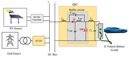
Figure 1.
Schematic structure of a QRC.
Several methodologies have been suggested to mitigate the voltage and current stress on the components, as well as to minimize switching losses in converters [18,19,20]. Paper [21] describes a boost (BoC) converter with a switched inductor that has limited voltage gain, minimal current stress across the inductors, and significant switching stress. To overcome the reduced voltage gain, the paper [22] presents a voltage-lift (VL) switched-inductor dual-leg converter, with continuous current at the output and high gain voltage at a 40% duty ratio for the first and second switches and a 50% duty ratio for the third switch. Comparing the control complexity of proposed converter in [23], which has one switch, to the converter in [24] that has two identical switches having similar duty cycles and a third switch with a different duty cycle, is more complex. Table 1 shows the comparative analysis of the non-isolated converters present in the literature. From the analysis, it can be inferred that the suggested QRC has high gain and minimum components. Therefore, the QRC is suitable for EV charging. The voltage, current, thermal stresses in the MOSFET and the diodes, during the transition from ON and OFF states, damage the devices and shorten their lifespans [25]. This increases the device failure rate, the disaster rate, and requires earlier replacement of converter’s internal parts. The bathtub model [26], in Figure 2, is suitable for assessing component failure rates in various applications. Three intermittent zones exist based on the component lifespan in the bathtub curve. These zones contain infant mortality, continual failure, and wear-out. Early device failure is extremely high, resulting in lower device reliability due to faulty installation, application, or design. Device analysis assumes a constant failure rate during a continual failure period. After a predefined life period, thermal and electrical stresses cause the device to reach the wear-out phase, increasing the failure rate.

Table 1.
Comparative analysis of converters.
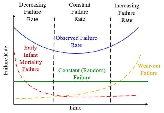
Figure 2.
Bathtub curve.
An evaluation of reliability is a type of method that describes the capacity of a component or a system to carry out its intended purpose, in accordance with a predetermined set of conditions over a period. The Markov model and fault traversal algorithm [27] are examples of different probability models that are frequently utilized. The Markov model accurately explains a stochastic process based on the state transition, making it an important tool for reliability analysis of a system that needs to be repaired. It is extensively employed to evaluate and predict system safety [28], and it has a considerable influence on the decision-making process for protecting a piece of equipment’s health status. Markov models are incorporated as a key strategy for addressing general probabilistic issues [29] and the reliability assessment of power electronic converters [30,31,32]. The methods of solving the Markov model include the Markov process and the semi-Markov process. This paper is organized as follows: the operating modes of the QRC, along with the mathematical modeling of converter, are presented in Section 2. Section 3 provides the parametric design details for the proposed QRC. Pulse generation using Xilinx for the prototype QRC is described in Section 4. Power loss analysis and the Markov model of the QRC are evaluated in Section 5 and Section 6. The results obtained from the Simulink platform and the low power QRC test rig are illustrated in Section 7. Finally, the inferences from the analysis carried out in Section 2, Section 3, Section 4, Section 5, Section 6, Section 7 and Section 8 are consolidated as the conclusions in Section 9.
2. Description, Operating Principle, and Modes of Operation of the QRC
Figure 3 depicts the designed power circuit of the QRC. This circuit contains one power-controlled switch (SW), three capacitors (C1BF, C2BF, and CL), and three inductors (LS, LBF, and LL), in addition to one uncontrolled switch (D). The controlled power switch, SW, transfers power from the grid (primary source) and PV (secondary source) to load (battery) based on the power demand. Consequently, the grid and PV are regarded as input ports, whereas the EV battery is coupled at the output port.
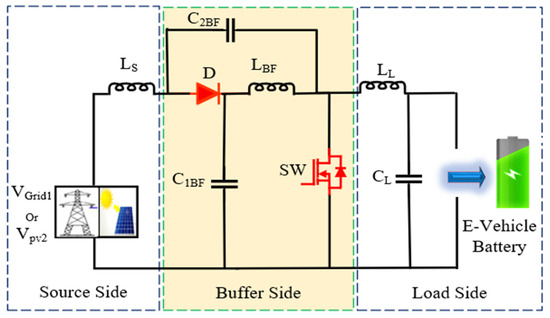
Figure 3.
Suggested QRC.
Figure 4 depicts different operating modes and the equivalent circuits for each interval in the operating period of the QRC. Table 2 describes the power transfer in the QRC during various modes of operation. The switch, diodes, capacitors, and inductors are assumed to be lossless components.
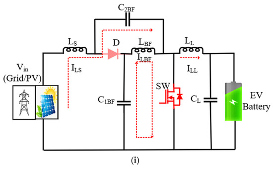
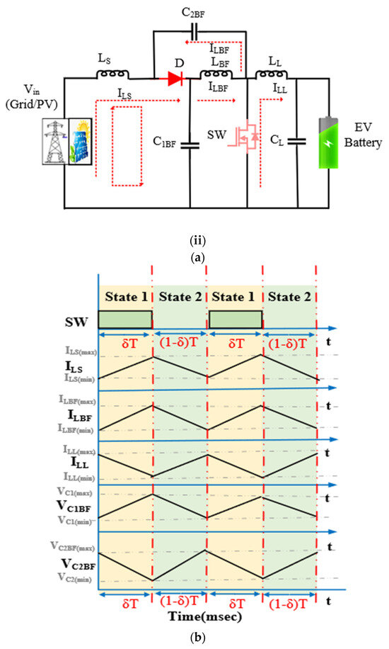
Figure 4.
Operation of the QRC: (a) equivalent circuit diagram, (i) when (Switch S = ON), (ii) when (Switch S = OFF); (b) characteristic waveform.

Table 2.
Various operating modes of the QRC.
Table 2.
Various operating modes of the QRC.
| Mode | Power Flow | Constraints |
|---|---|---|
| Mode 1 | Figure 5a. Grid to load battery | Grid power is sufficient (Pgrid > Pbat) |
| Mode 2 | Figure 5b. PV panel to load battery | PV power is sufficient (PPV > Pbat) |
| Mode 3 | Figure 5c. Grid and PV to load battery | PV and grid are sufficient (Pgrid + PPv) > Pbat) |
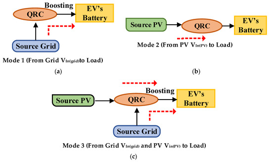
Figure 5.
Mode of power transfer operation of the QRC (a) Mode 1 (b) Mode 2 (c) mode 3.
2.1. Operating Principle
State 1: (0 < T < δT), the switch SW is turned on as depicted in Figure 4a. The current ILS through the inductor LS increases, with a positive slope. The discharging capacitor C2BF magnetizes the inductor LBF and charges the capacitor C1BF. As a result, inductor LL and capacitor CF are discharging. Equations (1)–(5) represent the operation in state 1.
State 2: (δT < T < T), the switch SW is in the off state as illustrated in Figure 4b. As a result, there is a dip in the inductor current ILS, with a negative slope. The inductor LBF demagnetizes and the capacitor C1BF discharges. LL and C2BF charge. The steady state condition of the QRC during state 2 is discussed using Equations (6)–(10).
The volt-second balance Equations (1)–(10) with respect to the inductor current and the charge-second balance equations with respect to the capacitor voltage are used to calculate the capacitor’s voltages and voltage gain (11)–(14).
2.2. Modes of Operation
Mode 1—(Vin(grid) > Vin(PV)) single input, single output: (Pgrid > PEV’S Battery) Figure 5a depicts the equivalent circuit of the QRC, as well as the power flow schematic while the converter is operating in mode 1. During such conditions, the grid delivers energy individually to charge the EV battery.
Mode 2—(Vin(PV) > Vin(grid)) single input, single output: (PPV > PEV’S Battery). During the daytime, the PV provides sufficient power to cater to the load demand. This mode delivers energy from PV to the EV battery individually, as depicted in Figure 5b.
Mode 3—(Vin(PV) = Vin(grid)): (Pgrid and PPV > PEV’S Battery). When the demand for EV battery power is significant, the grid and PV provide the required energy to meet the EV demand. As depicted in Figure 5c, both the PV and the grid provide energy to the battery in this scenario. During this state, the switch ‘SW’ is activated.
3. Parametric Design of the Proposed QRC
3.1. Choice of Switches and Diode
The QRC operates under various modes of operation. The power, voltage, and current handling capacities under each operating mode determine which semiconductor switch and diode need to be employed. The power management capability of each mode, namely the peak reverse blocking voltage and peak current, are considered when selecting a MOSFET switch SW with a body diode D for the proposed architecture. Using maximum battery voltage (VS = max (|vs, Vb|), the peak voltage rating for the SW is calculated. The peak current rating of the SW is regulated by the peak battery current.
3.2. Inductor
The inductor current ripple is essential for the inductor design. Equation (15) represents the current ripple after taking the voltage across the inductor ‘LS’ into account.
Inductors are designed to limit twice the magnitude of the ripple current differential. The inductor current ILS should oscillate within 20% of the average current. Equation (16) helps to design inductors LS by utilizing the appropriate current ripple and volt–sec balancing.
where f(sw) represents the switching frequency.
Also, the value of the inductor LBF and LL are estimated as mentioned by Equation (17).
3.3. Capacitor
The capacitors are considered to limit the change in voltage (ΔVC), as mentioned by Equation (18). According to an assumption, the permissible value of ΔVC1BF is 20% of the designed average capacitor voltage (VC1BF).
Using the capacitor charge–sec balance and voltage ripple, the capacitor C1BF is designed. C2BF and CL capacitor values are designed in a similar way using Equation (19).
4. Code Generation Using Xilinx ISE (VHDL)
As shown in Figure 6, with the assistance of FPGA and VHDL coding, Xilinx ISE 14.7 generates the pulse for the QRC. Xilinx ISE 14.7 is suitable for writing VHDL code and feeding it into the FPGA processor. Table 3 provide the parameter details of QRC for both simulation and experimental.

Figure 6.
(a) Generation of the pulse at the 0.4 duty cycle. (b) Block diagram of the PWM generation in the FPGA.

Table 3.
Parameter details of the QRC.
Coding
Figure 7 illustrates the generation of the switching pulse with the 0.4 duty ratio, using VHDL code. The generated switching pulse pattern for the 0.4 duty cycle using PWM techniques in the Xilinx platform is shown in Figure 8.
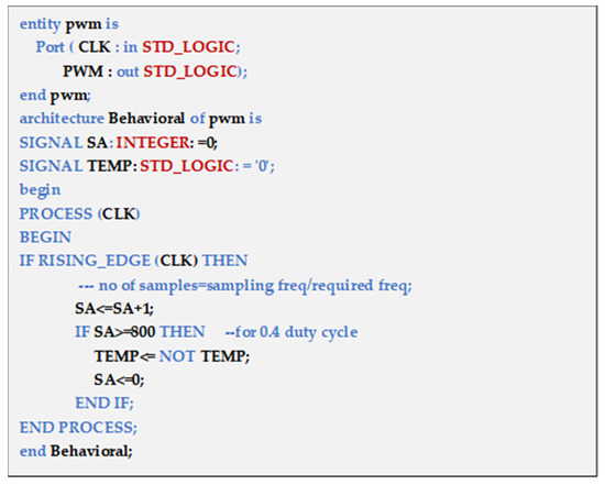
Figure 7.
Switching pulse using VHDL code.
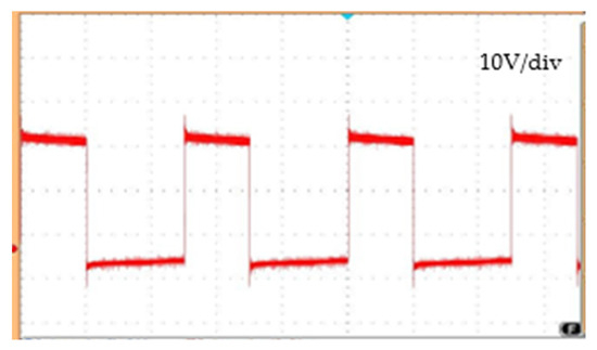
Figure 8.
Pulse generated using VHDL code.
5. Analysis and Comparison of the QRC
Power Loss
The following parasitic parameters were evaluated to study the QRC efficiency and reliability: Switch ON—state resistance RDS(ON), rFD—forward resistance (MOSFET), VT—threshold voltage, IS—switch current.
The total power loss of the MOSFET SW can be determined by Equation (20).
Equation (21) depicts the formula to evaluate the switch conduction loss (PrsL):
The QRC switch output current and duty cycle are ‘Io’ and ‘δ’, respectively. Equation (22) is used to estimate the MOSFET switching loss (PSL).
Vin, CS, and fs are the input voltage, snubber capacitor, and switching frequency respectively. Equations (21) and (22) are substituted into Equation (20) to derive MOSFET power losses is depicted in Equation (23).
Table 4 shows the switch’s total power loss (PMOSFET) for a constant voltage of 10 V and a variable duty cycle.

Table 4.
Analysis of the QRC for various duty cycles.
The total diode D (PD) power loss can be determined by Equation (24).
The diode’s ‘D’ forward resistance loss (PFR) can be calculated by Equations (23) and (24).
where rD and ID are the diode resistance and current, respectively.
The forward voltage loss of the diode (PFV) can be computed using Equation (26).
Substituting Equations (25) and (26) into Equation (24), the total power loss of the diode is evaluated using Equation (27).
PD = 0.508 W (for D = 40%, Vin = 10 V)
6. Comparative Analysis of Converters
Figure 9 provides the comparative analysis of conventional converters with the QRC, based on the efficiency and duty ratio. Various DC/DC converters’ switches, transformers, diodes, capacitors, and inductors need to be considered while designing a charging system. QRC topologies are inexpensive, as they have fewer components than conventional boost converters. BC [27], IBC [30], and ZVS [12] converters are uneconomical because of their high component count and HFT or the need to use many inductors. Voltage gain is also significant in system design. A boost converter is exclusive in that it only needs a conventional control system. The fundamental circuitry is simple and cost effective, but more capacitors increase its size, making it inappropriate for high-power conversion. IBC can provide maximum efficiency at 91% full load and less current ripples, but with high losses. Also, IBC requires EMI suppression. Table 5 summarizes the comparison of the QRC with various DC/DC converters.
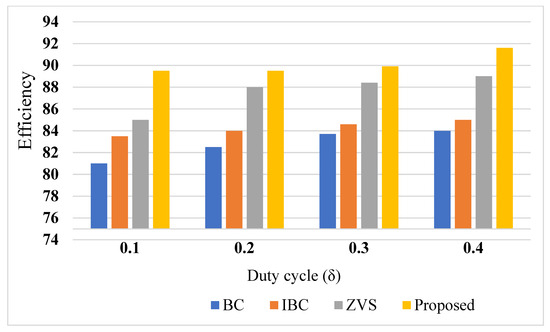
Figure 9.
Comparative analysis of the converters.

Table 5.
Comparison summary of the QRC with various DC/DC converters.
7. Markov Model for the QRC
The Markov approach is one of the analytical methods for assessing system reliability that has gained acceptance in recent years. The Markov reliability model consists of state-dependent failure rates. In this article, the continuous Markov model is used to determine the reliability performance of the QRC. Figure 10 depicts the corresponding Markov model based on the operation of the QRC under various faults, where the conditions of the QRC are characterized by four operating states. State 1 is a healthy state, state 2 and 3 are derated states, and state 4 is the failure condition of the QRC. The initial and final states represent the healthy and absorbing states, while the middle states represent the derated states. The failure rate of the QRC from state 1 to 2 and 4 are defined in Table 6. In Table 6, λMOSFET, λD, λL, and λC denote the failure rates of the MOSFET, diode, inductor, and capacitors which are elucidated from the power loss calculations and the MIL-HDBK-217F failure rate equations [30]. In addition, the probabilities of short circuit (SC) failures in each semiconductor MOSFET switch and diode are assumed as αSW (the SC probability of the SW) and αD (the SC probability of the D), respectively. Based on the research conducted, it is understood that the chance of an SC liability in power electronic semiconductor devices is significantly larger than the probability of an OC fault [23]. As a result, if a switch or a diode experiences a defect, the probability of having an SC fault or an OC fault are 75 percent and 25 percent, respectively. In addition, components are only susceptible to SC faults because of the operating characteristics, and these assumptions are enforced as λijs. Moreover, λijs is the failure rate of the QRC in various conditions and states.
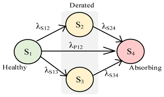
Figure 10.
Markov model for the QRC.

Table 6.
QRC transition failure rates.
In accordance with the Markov model in Figure 10, the QRC’s reliability performance is equivalent to:
where Px(t) represents the chance of operating state 1 at time t, and s represents the total number of operating states, which can include both healthy and derated states. To get the value of Px(t), the equation for a state–space matrix must be taken into consideration:
where λSxy (x ≠ y) is the failure rate from state x to y. Moreover, λSxy is defined as the negative sum of the failure rates in row x, and the sum of each row’s elements must be equal to zero [28]. The failure probability of each transition is shown in Table 6.
8. Result Analysis for the QRC
8.1. Simulation Results
Simulations were carried out with the help of MATLAB/Simulink. An input voltage of 12 V is considered for the entire period of QRC operation. For the simulation, as depicted in Figure 11a, the grid, PV voltage, and current are Vg = 12 V, VPV = 12, V and Ig = 6.8 A, IPV = 6.7 A. The battery voltage and current are Vb = 24.8, V and Ib = 3.2 A, respectively. The gate signal and the inductor currents are assumed to be ILS, ILBF, and ILL. The average current through inductors ILSgavg, ILBFavg, and ILLavg are 6.8 A, 6.8 A, and 4.2 A, respectively. The capacitor voltages are C1BF and C2BF at a duty cycle of d = 0.4.
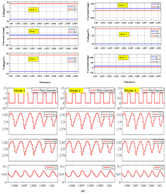
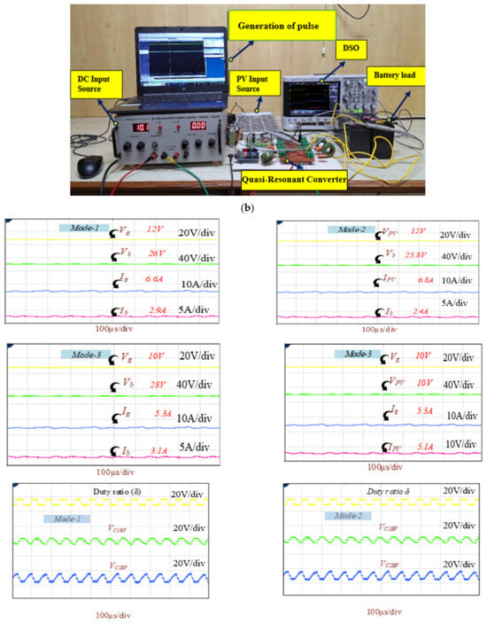
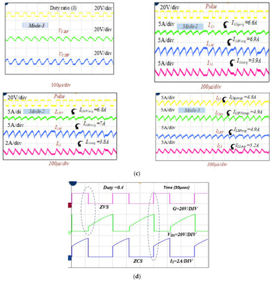
Figure 11.
Output voltage of the QRC: (a) simulation, (b) test rig of the QRC, (c) experimental, (d) experimental result for the switch current and voltage.
8.2. Experiment Results
The test rig, shown in Figure 11b, consists of the QRC converter with a PV and a DC supply, along with a battery as the load component. The proposed converter is analyzed under various testing conditions, with an input voltage of 12 V, and the experimental results are presented in Figure 11c.
As depicted in Figure 11c, the grid, PV voltage, and current are Vg = 12 V, VPV = 12, V and Ig = 6.6 A, IPV = 6.8 A. The battery voltage and current are Vb = 24.8, V and Ib = 2.9 A, respectively. The gate signal and the inductor currents are ILS, ILBF, and ILL. The average current of the inductors ILSgavg, ILBFavg, and ILLavg are 6.6 A, 6.9 A, and 3.9 A, respectively. The capacitor voltages are C1BF and C2BF at a duty cycle of d = 0.4. From Figure 11c, it can be understood that the experimental results are in coherence with the simulation results. However, when the converter operates beyond 0.38, the real-time losses that occur are significant and contribute to the variations in the converter gain. Figure 11d shows the attainment of ZVS and ZCS of the MOSFET SW. The distribution of the losses in QRC is depicted in Figure 12.
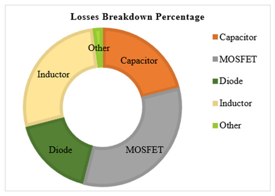
Figure 12.
Distribution of the losses (QRC).
9. Conclusions
A quasi-resonant converter is designed and implemented for an off-board charging station to operate with high gain at a low duty cycle and significantly reduce the charging time. The proposed QRC can operate under various operating conditions by utilizing the available sources during charging of the EV battery. Implementation of soft switching to the MOSFET, using the recommended converter, aids in reducing the switching losses. Also, a Markov model has been derived for the purpose of determining the failure rate possibilities of the QRC system. The simulation results in the MATLAB/Simulink platform and test rig results validate the viability of proposed EV off-board charger. A comparison of the QRC with conventional converters demonstrates its efficacy. The analysis of the proposed converter can be extended in future with the execution of the following work:
- Development of an optimized control strategy (CC-CV) for monitoring EV battery charging;
- Determination of component failure and reliability of the QRC using the MIL-HDBK-217F military handbook.
Author Contributions
H.S.: Conceptualization, Formal analysis and Investigation of Converter, Visualization, Writing—original draft. C.N.: Conceptualization of Methodology, Project administration, Supervision, Validation, Review of the original draft. M.J.H.: review and editing. All authors have read and agreed to the published version of the manuscript.
Funding
This research received no external funding.
Data Availability Statement
Data are contained within the article.
Conflicts of Interest
The authors declare no conflicts of interest.
References
- Singh, P.P.; Wen, F.; Palu, I.; Sachan, S.; Deb, S. Electric Vehicles Charging Infrastructure Demand and Deployment: Challenges and Solutions. Energies 2023, 16, 7. [Google Scholar] [CrossRef]
- Ihekwaba, A.; Kim, C. Analysis of electric vehicle charging impact on grid voltage regulation. In Proceedings of the 2017 North American Power Symposium (NAPS), Morgantown, WV, USA, 17–19 September 2017. [Google Scholar]
- Rong, X.; Wang, B.; Shao, C.; Yu, G.; Sun, Q.; Bie, Z. Coordinated charging strategy of electric vehicle charging station based on combination of linear power flow and genetic algorithm. In Proceedings of the 2016 IEEE PES Asia-Pacific Power and Energy Engineering Conference (APPEEC), Xi’an, China, 25–28 October 2016; pp. 1772–1776. [Google Scholar]
- Yilmaz, M.; Krein, P.T. Review of battery charger topologies, charging power levels, and infrastructure for plug-in electric and hybrid vehicles. IEEE Trans. Power Electron. 2013, 28, 2151–2169. [Google Scholar] [CrossRef]
- Taghizadeh, S.; Hossain, M.J.; Lu, J.; Water, W. A unified multi-functional on-board EV charger for power-quality control in household networks. Appl. Energy 2018, 215, 186–201. [Google Scholar] [CrossRef]
- Taghizadeh, S. A Multifunctional Single-Phase EV On-Board Charger with a New V2V Charging Assistance Capability. IEEE Access 2020, 8, 116812–116823. [Google Scholar] [CrossRef]
- Dubey, A.; Santoso, S. Electric Vehicle Charging on Residential Distribution Systems: Impacts and Mitigations. IEEE Access 2015, 3, 1871–1893. [Google Scholar] [CrossRef]
- Celli, G.; Soma, G.G.; Pilo, F.; Lacu, F.; Mocci, S.; Natale, N. Aggregated electric vehicles load profiles with fast charging stations. In Proceedings of the 2014 Power Systems Computation Conference, Wroclaw, Poland, 18–22 August 2014; pp. 1–7. [Google Scholar]
- Burnham, A.; Dufek, E.J.; Stephens, T.; Francfort, J.; Michelbacher, C.; Carlson, R.B.; Zhang, J.; Vijayagopal, R.; Dias, F.; Mohanpurkar, M.; et al. Enabling fast charging—Infrastructure and economic considerations. J. Power Sources 2017, 367, 237–249. [Google Scholar] [CrossRef]
- Forouzesh, M.; Siwakoti, Y.P.; Gorji, S.A.; Blaabjerg, F.; Lehman, B. Step-Up DC-DC converters: A comprehensive review of voltage-boosting techniques, topologies, and applications. IEEE Trans. Power Electron. 2017, 32, 9143–9178. [Google Scholar] [CrossRef]
- Lin, C.C.; Yang, L.S.; Wu, G.W. Study of a non-isolated bidirectional DC-DC converter. IET Power Electron. 2013, 6, 30–37. [Google Scholar] [CrossRef]
- Meinagh, F.A.A.; Babaei, E.; Tarzamni, H.; Kolahian, P. Isolated high step-up switched-boost DC/DC converter with modified control method. IET Power Electron. 2019, 12, 3635–3645. [Google Scholar] [CrossRef]
- Bao, D.; Kumar, A.; Pan, X.; Xiong, X.; Beig, A.R.; Singh, S.K. Switched Inductor Double Switch High Gain DC-DC Converter for Renewable Applications. IEEE Access 2021, 9, 14259–14270. [Google Scholar] [CrossRef]
- Karthikeyan, V.; Sundaramoorthy, K.; Kumar, G.G.; Babaei, E. Regenerative switched-inductor/capacitor type DC-DC converter with large voltage gain for PV applications. IET Power Electron. 2020, 13, 68–77. [Google Scholar] [CrossRef]
- Kawa, A.; Stala, R.; Mondzik, A.; Pirog, S.; Penczek, A. High-Power Thyristor-Based DC-DC Switched-Capacitor Voltage Multipliers: Basic Concept and Novel Derived Topology with Reduced Number of Switches. IEEE Trans. Power Electron. 2016, 31, 6797–6813. [Google Scholar] [CrossRef]
- Esteki, M.; Poorali, B.; Adib, E.; Farzanehfard, H. Interleaved Buck Converter with Continuous Input Current, Extremely Low Output Current Ripple, Low Switching Losses, and Improved Step-Down Conversion Ratio. IEEE Trans. Ind. Electron. 2015, 62, 4769–4776. [Google Scholar] [CrossRef]
- Shereef, N.K.; Mani, N.; John, N. A Novel DC-DC Boost Converter Based on Voltage-Lift Technique. Int. J. Innov. Eng. Technol. 2018, 11, 61–68. [Google Scholar]
- Harini, S.; Chellammal, N. A Novel High Gain Dual Input Single Output Z-Quasi Resonant (ZQR) DC/DC Converter for Off-Board EV Charging. IEEE Access 2022, 10, 83350–83367. [Google Scholar] [CrossRef]
- Das, M.; Agarwal, V. Generalized Small Signal Modeling of coupled-inductor-based high-gain high-efficiency DC–DC converters. IEEE Trans. Ind. Appl. 2017, 53, 2257–2270. [Google Scholar] [CrossRef]
- Yuan, B.; Liao, L.; Ning, G.; Xiong, W.; Su, M. An Expandable High Voltage-Gain Resonant DC-DC Converter with Low Semiconductor Voltage Stress. IEEE Trans. Circuits Syst. II Express Briefs 2022, 69, 3844–3848. [Google Scholar] [CrossRef]
- Karthikeyan, V.; Kumaravel, S.; Guru Kumar, G. High Step-Up Gain DC-DC Converter with Switched Capacitor and Regenerative Boost Configuration for Solar PV Applications. IEEE Trans. Circuits Syst. II Express Briefs 2019, 66, 2022–2026. [Google Scholar] [CrossRef]
- Tang, Y.; Fu, D.; Wang, T.; Xu, Z. Hybrid switched-inductor converters for high step-up conversion. IEEE Trans. Ind. Electron. 2015, 62, 1480–1490. [Google Scholar] [CrossRef]
- Samiullah, M.; Iqbal, A.; Ashraf, I.; Maroti, P.K. Voltage Lift Switched Inductor Double Leg Converter with Extended Duty Ratio for DC Microgrid Application. IEEE Access 2021, 9, 85310–85325. [Google Scholar] [CrossRef]
- Tarzamni, H.; Babaei, E.; Gharehkoushan, A.Z.; Sabahi, M. Interleaved full ZVZCS DC-DC boost converter: Analysis, design, reliability evaluations and experimental results. IET Power Electron. 2017, 10, 835–845. [Google Scholar] [CrossRef]
- Yao, B.; Chen, H.; He, X.Q.; Xiao, Q.Z.; Kuang, X.J. Reliability and failure analysis of DC/DC converter and case studies. In Proceedings of the 2013 International Conference on Quality, Reliability, Risk, Maintenance, and Safety Engineering (QR2MSE), Chengdu, China, 15–18 July 2013; pp. 1133–1135. [Google Scholar]
- Alam, M.K.; Khan, F.H. Reliability analysis and performance degradation of a boost converter. IEEE Trans. Ind. Appl. 2014, 50, 3986–3994. [Google Scholar] [CrossRef]
- Tarzamni, H.; Tahami, F.; Fotuhi-Firuzabad, M.; Blaabjerg, F. Improved Markov Model for Reliability Assessment of Isolated Multiple-Switch PWM DC-DC Converters. IEEE Access 2021, 9, 33666–33674. [Google Scholar] [CrossRef]
- Boudjellal, B.; Benslimane, T. Open-switch fault-tolerant control of power converters in a grid-connected photovoltaic system. Int. J. Power Electron. Drive Syst. 2016, 7, 1294–1308. [Google Scholar] [CrossRef]
- Tarzamni, H.; Esmaeelnia, F.P.; Tahami, F.; Fotuhi-Firuzabad, M.; Dehghanian, P.; Lehtonen, M.; Blaabjerg, F. Reliability Assessment of Conventional Isolated PWM DC-DC Converters. IEEE Access 2021, 9, 46191–46200. [Google Scholar] [CrossRef]
- Hamoud, G.A.; Yiu, C. One Markov Model for Spare Analysis of Distribution Power Transformers. IEEE Trans. Power Syst. 2016, 31, 1643–1648. [Google Scholar] [CrossRef]
- Jahan, H.K.; Panahandeh, F.; Abapour, M.; Tohidi, S. Reconfigurable Multilevel Inverter with Fault-Tolerant Ability. IEEE Trans. Power Electron. 2018, 33, 7880–7893. [Google Scholar] [CrossRef]
- Tarzamni, H.; Babaei, E.; Esmaeelnia, F.P.; Dehghanian, P.; Tohidi, S.; Sharifian, M.B.B. Analysis and Reliability Evaluation of a High Step-Up Soft Switching Push-Pull DC-DC Converter. IEEE Trans. Reliab. 2020, 69, 1376–1386. [Google Scholar] [CrossRef]
Disclaimer/Publisher’s Note: The statements, opinions and data contained in all publications are solely those of the individual author(s) and contributor(s) and not of MDPI and/or the editor(s). MDPI and/or the editor(s) disclaim responsibility for any injury to people or property resulting from any ideas, methods, instructions or products referred to in the content. |
© 2024 by the authors. Licensee MDPI, Basel, Switzerland. This article is an open access article distributed under the terms and conditions of the Creative Commons Attribution (CC BY) license (https://creativecommons.org/licenses/by/4.0/).