Article

Applying a Current Sharing Method Based on Partial Energy Processing to Multiphase LLC Resonant Converters

1
Delta Electronics Inc., No. 186, Ruiguang Road, Neihu District, Taipei 114501, Taiwan
2
Monolithic Power Systems: MPS, 29F, No. 97, Section 1, Xintai 5th Road, Xizhi District, New Taipei City 22175, Taiwan
3
Department of Electrical Engineering, National Taipei University of Technology, No. 1, Section 3, Zhongxiao East Road, Taipei 10608, Taiwan
*
Author to whom correspondence should be addressed.
Energies 2024, 17(15), 3859; https://doi.org/10.3390/en17153859
Submission received: 13 July 2024 / Revised: 1 August 2024 / Accepted: 3 August 2024 / Published: 5 August 2024
(This article belongs to the Special Issue Optimal Design and Application of High-Performance Power Converters)

Abstract

:
In this paper, partial energy processing is applied to the current sharing technique for multiphase LLC resonant converters. The proposed circuit consists of an LLC resonant converter and a flyback converter, where the flyback converter is only used for partial energy processing. The input voltage of the LLC resonant converter is fine-tuned by the flyback converter to solve the problem of a voltage gain difference between the two phases of the LLC resonant converter caused by the error of the resonant tank components, which prevents the output current from being nonequalized. Since the compensation power is much smaller than the output power, and only one phase will be during circuit operation, the impact on the overall efficiency is minimal. Due to the low dependence between the LLC resonant converter and the flyback converter, they are operated at different switching frequencies. In addition, due to the low dependence between each phase, the circuit can be expanded using odd and even phases.

1. Introduction

The increase in network traffic has raised the importance of data centers to meet and properly manage these growing demands. The data center is one of the most energy-intensive building types, consuming 10 to 50 times more energy per floor of space than a typical commercial office building, and these values are growing every year. As shown in Figure 1, where VRM is the abbreviation for the voltage-regulated module, in a traditional structure, major processor/memory devices are powered by 12 V, and the uninterruptible power system (UPS) is placed on the high voltage side. As shown in Figure 2, compared with the traditional 12 V structure, the 48 V structure can reduce the copper loss and bus loss by 16 times. In addition, the UPS can be placed on the low-voltage side, so it has the advantages of high efficiency, low cost, and small size [1,2]. The 48 V structure complies with the international electrotechnical commission (IEC) 60335-1 safety extra low voltage (SELV) standard [3]. Because of these advantages, Google has started using the 48 V structure in its data centers [4], and this structure has been widely used in LED panels, power tools, automobiles, and telecommunication systems [5].
Distributed power systems (DPSs), widely used in data centers and telecommunication systems, have the advantages of thermal management, reliability, maintainability, high flexibility, and high efficiency [6]. Therefore, LLC resonant converters are widely used as front-end isolation converters in DPS systems. The DC transformer (DCX) has many advantages. For example, the switches of the half-bridge LLC resonant converter switch near the resonant frequency with a duty cycle close to 50%. There is no voltage control loop, so the best efficiency can be obtained. At the same time, the zero-voltage switching (ZVS) turn-on for the primary side switches and the zero-current switching (ZCS) turn-off for the secondary side diodes function over all the load ranges. Due to the discontinuous output current of an LLC resonant converter, it is necessary to parallel multiple capacitors to suppress excessive ripple and heat generation, especially in high output current applications.
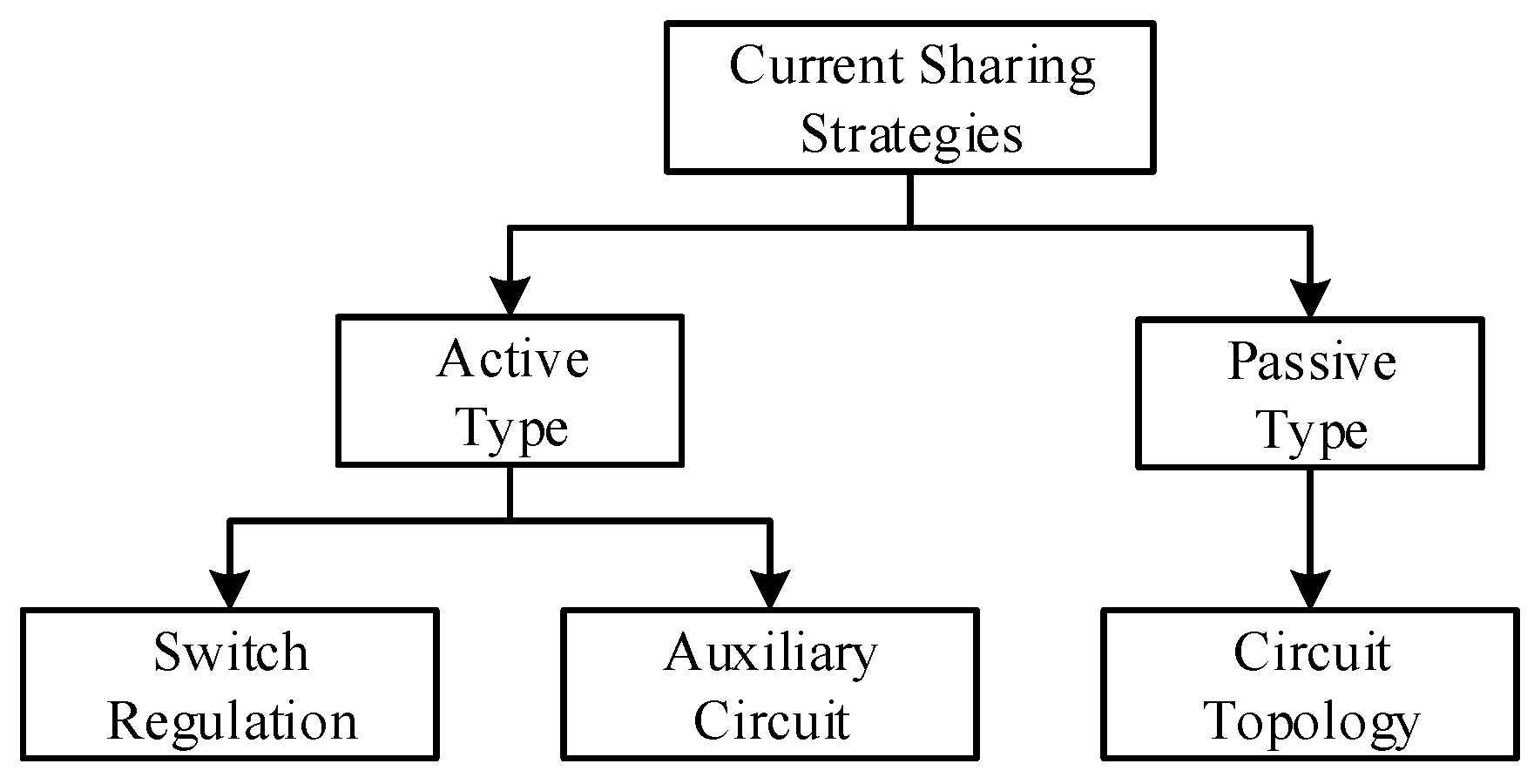
Multiphase power converters distribute the load current to each phase, thus effectively minimizing current ripple and spreading component losses and thermal stress [7]. Compared with the traditional single power converter, parallel power supplies can realize high efficiency in high power applications. However, in practice, due to a difference in the resonant tank components of each phase, the impedance of the resonant tanks varies from phase to phase, resulting in the current supplied by each phase being inconsistent. Therefore, how to balance the currents between the phases of an LLC resonant converter is an important issue in today’s research [8,9,10,11,12,13,14,15,16,17,18,19,20,21,22,23,24,25,26,27,28,29,30,31]. As shown in Figure 3, the general current sharing strategies for multiphase resonant converters can be classified into the circuit topology method [8,9,10,11,12,13,14,15,16,17], the switch regulation method [19,20,21,22,23,24,25], and the auxiliary circuit method [25,26,27,28,29,30,31].
The circuit topology method belongs to the passive current sharing method and is mainly used to change the connection of the circuit or to insert additional passive components into the circuit, so as to achieve the purpose of equalizing the current of each phase without additional control. The advantage of this method is that it does not need to additional complex control; however, when one of the converters is damaged, it will not work properly. The literature [8] proposes a way to parallelize the resonant capacitors of the two phases so that the resonant capacitors of the two phases of the LLC resonant converter can be regarded as the same one in the equivalent circuit; hence, the current sharing can be achieved. Based on a similar concept, the literature [9] proposes a way to parallelize the resonant inductors of the two phases so that the resonant inductors of the two phases of the LLC resonant converter can be considered as the same one in the equivalent circuit. Thus, the current sharing can be realized, but it is not applicable to the circuit in which the leakage inductance of the main transformer is used as the resonant inductor. The two-phase LLC resonant converter of the literature [10] uses the same resonant inductor and half-bridge circuit, so the circuit size can be effectively reduced. However, when the leakage inductances of the main transformers of the two-phase LLC resonant converter are different, the current sharing performance will be influenced. The literature [11] proposes a secondary winding integration method to achieve output current sharing by connecting the secondary windings of the two-phase LLC resonant converter in series. The literature [12] proposes a primary side resonant tank integration method to achieve equalization of the secondary current by connecting the resonant tanks in series. The literature [13] proposes a common-mode transformer added to the resonant tank between two phases of the LLC resonant converter to utilize the characteristics of the transformer for current sharing. The literature [14] presents a current sharing method using the ampere-second balance of a capacitor. Due to the characteristics of the capacitor, this circuit can only be applied to two phases of the LLC resonant converter, but it is not possible to expand the phase count. The above-mentioned technique realizes current sharing by means of the circuit topology or the passive element, so there is no need for additional switch control; thus, it has the advantage of simple control. However, due to the limitation of the connection between the passive element and the circuit, the main switch of each phase circuit has to be switched synchronously. Therefore, the studies in the literature [8,9,10,11,12,13,14] do not have the advantage of reducing the current ripple. Compared with the above-mentioned circuits, although the passive current sharing method is also adopted in the literature [15,16,17], the main switch of each phase circuit does not need to be switched synchronously, so it has the function of reducing the output ripple. The literature [15] proposes a method to balance the current based on the output filter. The literature [16] adopts common-mode chokes to achieve current sharing in a three-phase LLC resonant converter. The literature [17] uses the input capacitors connected in series to automatically adjust the input capacitor voltages of the two phases when there is an error in the resonant tank element to realize the purpose of balancing the currents in a two-phase LLC resonant converter.
Compared to the passive current sharing method mentioned above, the switch regulation method and the auxiliary circuit method are active current sharing methods. For the switch regulation method to be considered, it needs to realize the purpose of current balance by modulating the switching frequency or duty cycle of the switch, which has relative advantages in design and cost since it does not require the use of an additional auxiliary circuit. The literature [18] presents an LLC resonant converter to adjust the voltage gain by varying the switching frequency to achieve current sharing. Although this is easier to realize, it will produce a larger output current ripple. The literature [19] proposes a phase shift control strategy to adjust the phase difference between the input voltages of the resonant tanks to realize current sharing, but the design needs to consider the phase of the resonant current so as to avoid loss of the ZVS feature. The literature [20] presents a way to control the width of the duty cycle to realize current balancing. The literature [21,22,23,24] presents a way to replace the secondary side rectifier diode with an active switch or to use an additional active switch and then to adjust the on-time of the switch to change the equivalent resistance mapped back to the primary side to achieve the purpose of current equalization.
In contrast to the switch regulation method, the auxiliary circuit method utilizes an applied circuit for current balancing. The literature [25,26] presents a variable capacitor composed of an active switch and a capacitor to achieve current equalization by adjusting the on-time of the active switch and changing the capacitance of the resonant capacitor to compensate for the difference in impedance of the resonant tanks between phases. The literature [27] proposes a variable inductor by applying the phenomenon that the relative permeability of ferromagnetic materials decreases with the increase of magnetic field strength. Due to the presence of an auxiliary winding and a controllable current source, the Inductance is changed by controlling the auxiliary winding current to establish the corresponding bias magnetic field strength during circuit operation; however, the additional iron losses increase the losses. The literature [28] presents a method of adding a pre or post converter to each phase of the LLC resonant converter and then adjusting the voltage gain of each phase through the pre or post converter to achieve current equalization; however, this method needs to be considered in terms of cost and efficiency. In order to solve the problem of efficiency degradation caused by the two-stage structure, the literature [29,30,31] propose a low-power circuit with partial power processing. In [29], an isolated low-power auxiliary DC-DC converter is added to the resonant tank of each phase of the LLC resonant converter, and the purpose of equalizing the current is realized by adjusting the duty cycle of the switch of the DC-DC converter. Similar to [29], the auxiliary circuit in [30] is a phase shift full bridge (PSFB) circuit where the transformer of the auxiliary circuit is integrated with the main transformer of the LLC resonant converter. The auxiliary circuit in [31] utilizes a buck-type converter, but it has the disadvantage that the primary and secondary sides are not isolated. Since the phase current balancing is achieved by the auxiliary circuit, the auxiliary and main circuits can usually be operated independently of each other, which provides a simpler control strategy as compared to the switch regulation method. The current sharing approach based on partial energy processing offers several advantages in such scenarios by managing the nonlinear characteristics of inductors [32,33,34], ensuring stable and precise current control, and reducing the electromagnetic interference (EMI). In addition, a three-phase LCL filter is designed for grid-connected PWM inverters using hybrid bacteria foraging and particle swarm optimization [35].
Based on that mentioned above, this paper presents the partial energy applied to the current equalization of the two-phase LLC resonant converter, which is realized by fine-tuning of the input voltage of the resonant tank through the flyback converter to change each phase voltage gain so that each phase impedance can be as identical as possible so as to achieve current equalization between the two phases. The limitations of this circuit are relatively high cost and relatively complex control method. However, the proposed circuit is suitable for driving LED strings. In addition, the proposed methodology is different from those reported in the literature [11,14,22,29,30]. Consequently, the following are the advantages and objectives of the proposed circuit:
(1)
Dependent voltage source circuits provide only part of the input voltage in steady state, so the power required is very low;
(2)
Dependent voltage source circuits have quite low dependence on the main circuits and can be operated and regulated independently of each other;
(3)
The two-phase main circuits can reduce output current ripple due to interleave operation;
(4)
As the output power required by the load has to be increased, the overall power can be increased by increasing the number of phases.

2. Main Power Stage

Figure 4 shows the structure of the single-phase circuit proposed in this paper, which consists of an LLC resonant converter combined with a flyback converter. In addition, the multiphase system can be expanded by this circuit, and each phase can operate independently of each other with the same mode of operation. Figure 5 displays the two-phase LLC resonant converter with partial energy processing proposed in this paper. The first phase consists of four switches S1, S2, S3, and S4; a resonant inductor Lr1; a resonant capacitor Cr1; an output capacitor Co1; and a transformer Tr1, which consists of a magnetizing inductor Lm1 combined with an ideal transformer. The primary and secondary coils of the transformer are denoted by Np1 and Ns1, respectively. The corresponding flyback converter is composed of a switch S5, a diode D1, an output capacitor Co2, and a transformer Tr2, which consists of a magnetizing inductor Lm2 combined with an ideal transformer. The primary and secondary coils of the transformer are signified by Np2 and by Ns2, respectively. The second phase consists of four switches S6, S7, S8, and S9; a resonant inductor Lr2; a resonant capacitor Cr2; an output capacitor Co3; and a transformer Tr3, which is composed of a magnetizing inductor Lm3 combined with an ideal transformer. The primary and secondary coils of the transformer are denoted by Np3 and Ns3, respectively. The corresponding flyback converter contains a switch S10, a diode D2, an output capacitor Co4, and a transformer Tr4, which is composed of a magnetizing inductor Lm4 combined with an ideal transformer. The primary and secondary coils of the transformer are signified by Np4 and Ns4, respectively. Also, the input voltage is Vdc, the output voltage is Vo, and the dependent voltages Vctrl1 and Vctrl2 come from the individual flyback converters. Moreover, in Figure 4 and Figure 5, the symbols of voltages and currents correspond to the individual components.

3. Current Sharing Technique Analysis of the Proposed Circuit

In this section, partial energy processing is applied to current sharing for the multiphase LLC resonant converter, where the input voltage to the resonant tank is fine-tuned by the flyback converter to compensate for the difference in voltage gain due to component tolerance of the multiphase LLC resonant converter. Accordingly, how the flyback converter works with the LLC multiphase resonant converter to realize current sharing is described in detail herein.

3.1. LLC Voltage Gain

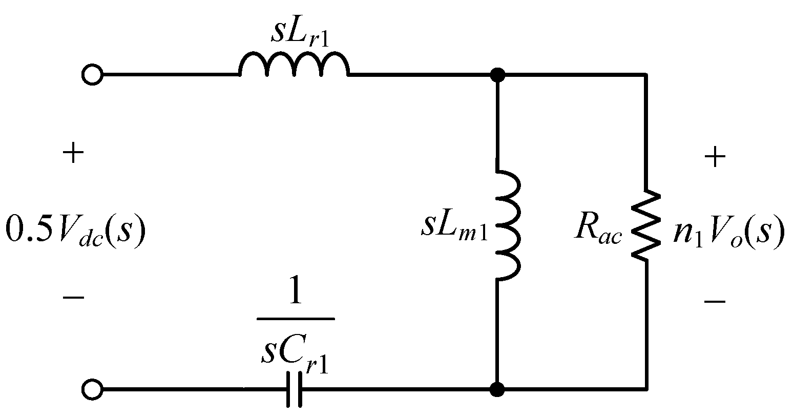
The voltage gain of the LLC resonant converter is analyzed in this section. The half-bridge LLC resonant converter is designed to switch the two switches at a high frequency to change the impedance of the resonant tank so as to transfer the energy to the rear stage. At the same time, it adopts a constant frequency and drives the two switches with complementary driving signals having a duty cycle of about 50%. In addition, the quality factor Q of the circuit, the ratio K of the magnetizing inductance Lm1 to the resonance inductance Lr1, the resonant radian frequency ωr1, and the switching radian frequency ωs1 need to be considered. Since the voltage across the switch S2, called vds2, is located between zero and the input voltage Vdc, this square wave voltage is analyzed using the first harmonic approximation (FHA) method. Specifically, only the fundamental wave component is considered, which is denoted by vin. Afterwards, the voltage gain of the LLC resonant converter will be analyzed. Figure 6 shows the equivalent circuit containing the resonant inductor Lr1, the resonant capacitor Cr1, the magnetizing inductance Lm1, and the equivalent resistance Rac, which is reflected from the load resistance Ro on the secondary side to the primary side, where the turns ratio n1 is equal to Np1 divided by Ns1, namely, n1 = Np1/Ns1. Therefore, Rac can be expressed as follows:
R a c = n 1 2 × 8 π 2 × V o I o 1
where Io1 is the output current.
Q = Z r 1 R a c = L r 1 C r 1 R a c = ω r 1 × L r 1 R a c
K = L m 1 L r 1
Eventually, the voltage gain MLLC1(s) is derived from the equivalent circuit in Figure 7 and is expressed as follows:
M L L C 1 ( s ) = n 1 V o s 0.5 V d c s = s L m 1 / / R a c s L r 1 + 1 s C r 1 + s L m 1 / / R a c = s 2 × L m 1 L r 1 × 1 ω r 1 2 s 3 × L m 1 L r 1 × L r 1 ω r 1 R a c × 1 ω r 1 3 + s 2 × 1 ω r 1 2 × 1 + L m 1 L r 1 + s ω r 1 × ω r 1 L r 1 R a c × L m 1 L r 1 + 1
Equation (4) can be simplified as follows:
M L L C 1 ( s ) = s ω r 1 2 × K s ω r 1 3 × K × Q + s ω r 1 2 × 1 + K + s ω r 1 × Q × K + 1
Let s = s1 = jfs1 and ωr1 = 2πfr1. By substituting these expressions into (5), the corresponding magnitude MLLC1 can be obtained as follows:
M L L C 1 = n 1 V o 0.5 V d c = M L L C 1 ( j 2 π f s 1 ) = K × f s 1 f r 1 2 K + 1 × f s 1 f r 1 2 1 2 + f s 1 f r 1 3 1 × f s 1 f r 1 × Q × K 2
From (6), it can be seen that the voltage gain MLLC1 is affected by the parameters of Q and K.
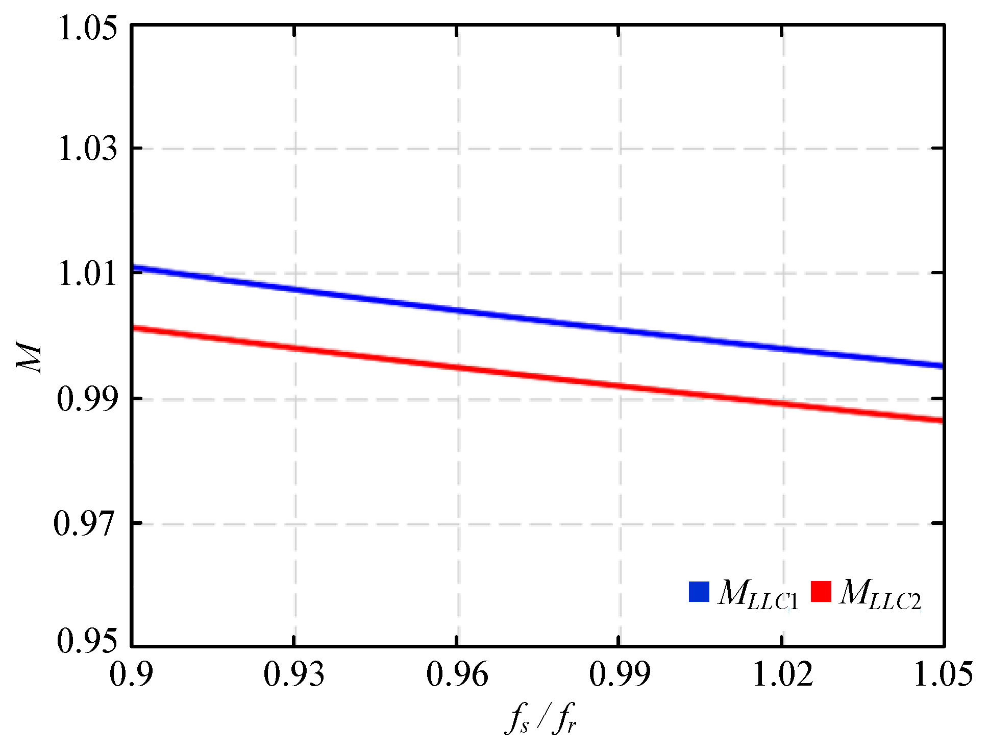
Assume that the resonant inductance Lr2 and the magnetizing inductance Lm3 of the second phase are 1.2 times that of the resonant inductance Lr1 and the magnetizing inductance Lm1 of the first phase, and the capacitances of the resonant capacitors Cr1 and Cr2 of the two phases are the same. The parameters of the two phases are brought into (6), and then the two voltage gain curves can be plotted, namely MLLC1 and MLLC2, as shown in Figure 8. As can be seen from this figure, the voltage gains are different at the same operating frequency due to errors in the passive component values in the resonant tanks, and this makes the output current provided by the two phases inconsistent.

3.2. Voltage Gain of the Proposed Circuit

In order to solve the problem that the output currents cannot be equalized due to the difference in impedance of the resonance tanks, a method of connecting a dependent voltage source in series with the input voltage is proposed, so that the voltage gain can be compensated by adjusting the voltage of the dependent voltage source. In addition, the voltage of the dependent voltage source in steady state is much smaller than the input voltage, so it is only necessary to use an isolated low-power DC converter to realize voltage gain compensation.
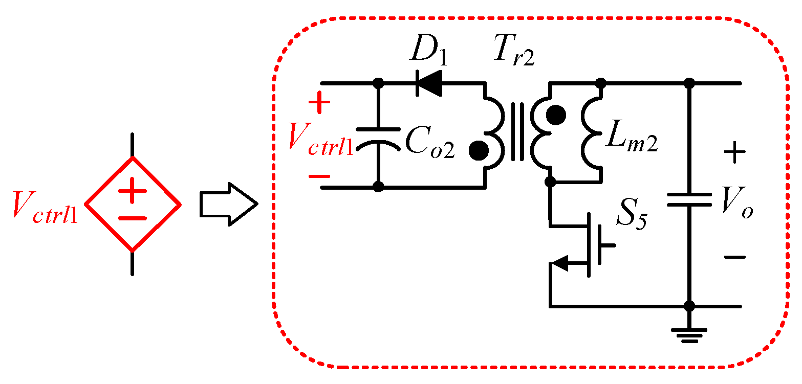
From Figure 4, the equivalent circuit of Figure 9 can be derived, and the difference between Figure 9 and Figure 6 is that the operating voltage of the resonant tank is composed of the dependent voltage Vctrl1 in series with the input voltage Vdc, where the dependent voltage Vctrl1 comes from the voltage-dependent source, named the flyback converter, as shown in Figure 10.
The voltage gain of the proposed circuit can be rewritten from (6) as follows:
0 . 5 V d c + V c t r l 1 × M L L C 1 = n 1 V o
Also, the voltage gain of the flyback converter is expressed as follows:
M f l y b a c k = V c t r l 1 V o = D n 2 1 D
where D is the duty cycle.
By substituting (8) into (7), the voltage gain M1(D) can be expressed as a function of the duty cycle D as below:
M 1 D = V o V d c = 0.5 M L L C 1 n 1 0.5 n 2 × D 1 D
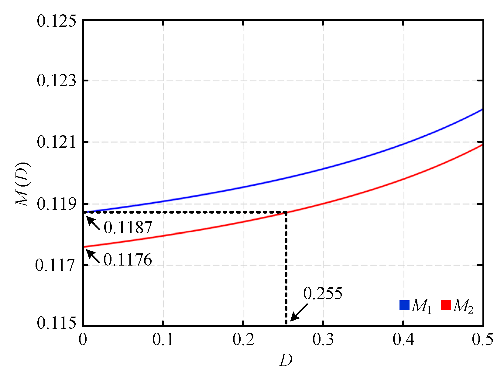
The resonant inductance Lr2 and magnetizing inductance Lm3 of the second phase are 1.2 times of the resonant inductance Lr1 and magnetizing inductance Lm1 of the first phase, respectively, and the capacitance of the resonant capacitors Cr1 and Cr2 of the two phases are the same. By substituting the required parameter values of the two phases into (9), the two voltage gain curves M1 and M2 can be drawn, where the horizontal axis is the duty cycle D for the flyback converter, as shown in Figure 11. As can be seen from this figure, under the same operating frequency, when the switches of both of the flyback converters are turned off (D1 = D2 = 0), the voltage gain of the phase 1 circuit (M1(0) = 0.1187) will be larger than that of the phase 2 circuit (M2(0) = 0.1176). This is due to the errors of the passive elements of the two resonant tanks, making the two phases not provide the same output current. Accordingly, the switch of the phase 1 circuit’s flyback converter (D1 = 0) is turned off, and the switch of the phase 2 circuit’s flyback converter is regulated (D2 = 0.255) to make the voltage gains of the two phases as close to the same as possible, so as to compensate for the failure of equalizing the output currents.

3.3. Extension of the Phase Account

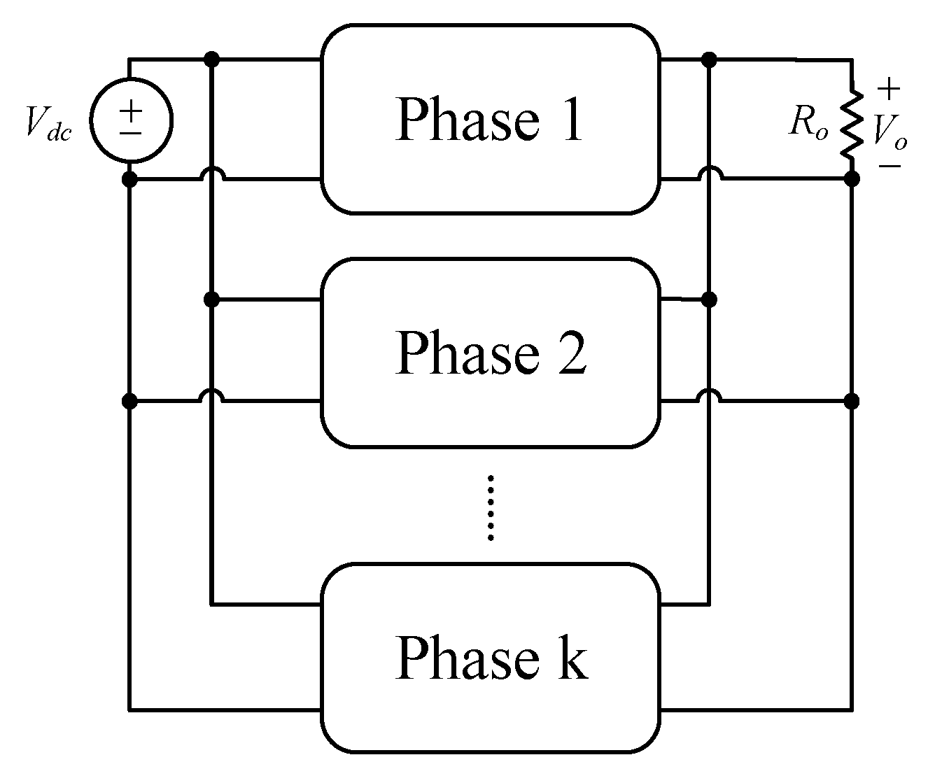
As shown in Figure 12, the proposed circuit can upgrade the overall power by increasing the phase account. Its operating principle and component design will not be redesigned, so it is quite convenient in practical applications.

4. Design Considerations

4.1. Parameter Design

The system circuit consists of an LLC resonant converter as well as a flyback converter, so that the power is expressed as follows:
P T = P o + P F l y b a c k
The total output power PT is the output power Po plus the consumption power PFlyback of the flyback converter. As shown in Table 1 and Table 2, PFlyback is much smaller than Po, so the effect of the flyback converter on the voltage gain of the LLC resonant converter can be ignored. Since the designs of two-phase LLC components are the same, the following is assumed: two LLC transformers Tr1 = Tr3 = Tr,LLC, two flyback transformers Tr2 = Tr4 = Tr,Flyback, two LLC turns ratios n1 = n3 = nLLC, two flyback turns ratios n2 = n4 = nFlyback, two LLC magnetizing inductances Lm1 = Lm3 = Lm,LLC, two flyback magnetizing inductances Lm2 = Lm4 = Lm,Flyback, two LLC resonant inductors Lr1 = Lr2 = Lr, two LLC primary side windings Np1,LLC1 = Np2,LLC2 = Np,LLC, two LLC secondary side windings Ns1,LLC1 = Ns2,LLC2 = Ns,LLC, two LLC resonant capacitors Cr1 = Cr2 = Cr, two LLC output capacitors Co1 = Co3 = Co,LLC, two flyback output capacitors Co2 = Co4 = Co,Flyback, and two flyback currents ids5 = ids10 = ids,Flyback. In order to obtain the error in the two-phase resonant inductances, this can be achieved by adjusting the air gap of the iron core.

4.1.1. Design of the Resonant Tank Parameter

The switching frequency of the two-phase LLC resonant converter is initially set at 110 kHz. In order to make the two-phase resonant inductances different from each other, namely, Lr2 = 1.2Lr1, the resonance frequency of the first-phase circuit is about 120 kHz, and the resonance frequency of the second-phase circuit is about 110 kHz, as shown in Table 1.

Selection of Turns Ratio nLLC of Tr,LLC

In this paper, the switching frequency of the LLC resonant converter is close to the first resonant frequency, so the voltage gain MLLC is approximated to be 1, which can be expressed as follows:
M L L C = 2 × n L L C V o V d c
By rearranging (11), the turns ratio nLLC (=Np,LLC/Ns,LLC) is shown below:
n L L C = M L L C × 1 2 × V d c V o = 1 × 1 2 × 400 48 = 4.17
Based on the calculation in (12), the turns ratio of nLLC is selected to be 4.25.

Determination of Output Equivalent Resistance Rac

The output load resistance Ro at rated load is shown below:
R o = V o I o 1 , r a t e d = 48 21 = 2.286   Ω
where Io1,rated is the rated output current.
Since the voltage gain will be affected by the load, the output resistance Ro should be equivalent to the primary side of the transformer Tr,LLC to facilitate the design and analysis of parameters of the resonant tank. By substituting the result of (13) into (1), the output equivalent resistance Rac is given as follows:
R a c = n L L C 2 × 8 π 2 × R o = 4.25 2 × 8 π 2 × 2.286 = 33.465   Ω

Determination of the Values of K and Q

From (2), when the load and switching frequency are fixed, the smaller the value of Lr is, the smaller the value of Q, and the smaller the value of Lr is, the smaller the parasitic resistance of the winding is. Thus, the value of Q is set at 0.2. In addition, with a fixed value of Lr, the larger the value of K is, the smaller the effect of load on voltage gain, and the circulating current generated by Lm,LLC will be reduced to improve the efficiency. However, if the value of K is too large, the primary side half-bridge switches will not be able to achieve ZVS turn-on. Consequently, based on the simulation software PSIM 9.11, the ZVS condition can be satisfied by setting the value of K at 20.

Determination of the Values of Lr, Cr and Lm,LLC

Since the value of Q is 0.2, and the resonance frequency fr is 120 kHz, the resonant capacitance Cr is calculated as 198.161 nF, as shown in (15):
Q = L r C r × 1 R a c = 1 2 π × f r × R a c × C r C r = 1 2 π × Q × f r × R a c C r = 1 2 π × 0.2 × 120 × 10 3 × 33.465 = 198.161 nF
Therefore, the selected resonant capacitance Cr is 220 nF, and the resonant inductance Lr can be determined using the resonant capacitance Cr and the resonant frequency fr.
f r = 1 2 π L r × C r L r = 1 2 π × f r 2 × C r L r = 1 2 π × 120 × 10 3 2 × 220 × 10 9 = 7.996   μ H
Based on (16), the required magnetizing inductance Lm,LLC can be obtained as follows:
L m , L L C = K × L r = 20 × 7.996 × 10 6 = 159.913   μ H

4.1.2. Design of Flyback Converter Parameter

The magnetizing inductance of the flyback converter will be figured out as below.

Selection of Turns Ratio nFlyback of Tr,Flyback

According to [36], Dmax is set at 0.45, and the turns ratio nFlyback (=Np,Flyback/Ns,Flyback) is expressed as follows:
n F l y b a c k = V o × D m a x V c t r l , m a x × 1 D m a x = 48 × 0.45 10 × 1 0.45 = 3.927
Based on (18), the turns ratio of nFlyback is chosen as 3.667.

Determination of the Value of Lm,Flyback

In order to ensure that the flyback converter can operate in the continuous conduction mode (CCM) when the output current Iin1 is above the minimum current of 1 A, Equation (19) is obtained as follows:
L m , F l y b a c k , B C M = V o × D m a x 2 2 I i n 1 , m i n × V c t r l 1 × f s 2 = 48 × 0.45 2 2 × 1 × 10 × 100 × 10 3 = 233.28   μ H
where Lm,Flyback,BCM means the magnetizing inductance Lm,Flyback for the flyback converter operating in the boundary conduction mode (BCM). Lm,Flyback should satisfy the condition of Lm,Flyback > Lm,Flyback,BCM.

5. System Control Strategy

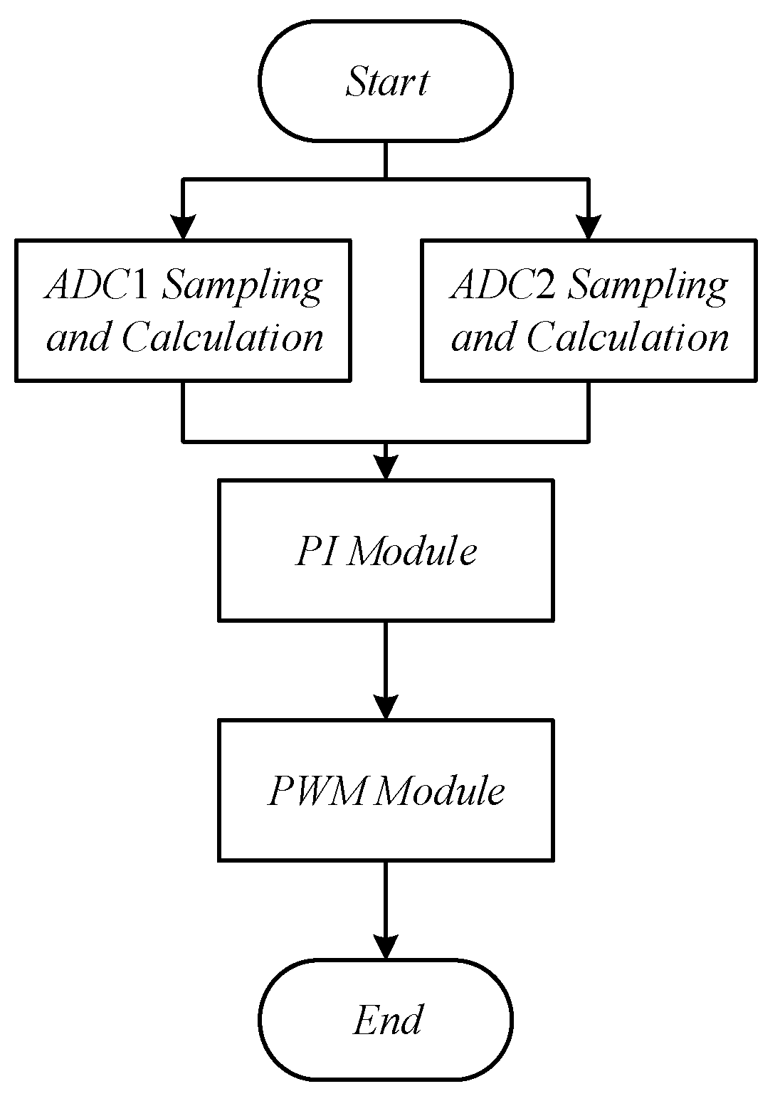
Figure 13 shows the main program flow chart, which consists of two analog-to-digital converters (ADCs) for sampling and data calculation, a proportional-integral (PI) module with 12-bit ADCs, and a pulse-width modulation (PWM) module with a 16-bit PWM. It is noted that the system functions required will be accomplished within one PWM cycle. Afterwards, the associated signals will be sent to the PI module and then to the PWM module to generate suitable control forces to drive the switches.

5.1. ADC Sampling Triggering and Data Calculation

Figure 14 shows the program flowchart of ADC sampling triggering and data calculation. As PWM1 triggers sampling and calculation of ADC1 and ADC2, the former is responsible for the phase 1 output current, whereas the latter is responsible for the phase 2 output current. After this, the resulting digital current signal Io2 is subtracted from the resulting digital current signal Io1, namely, Io1Io2, to obtain an error signal, called Error, which will be sent to the PI module.

5.2. PI Module

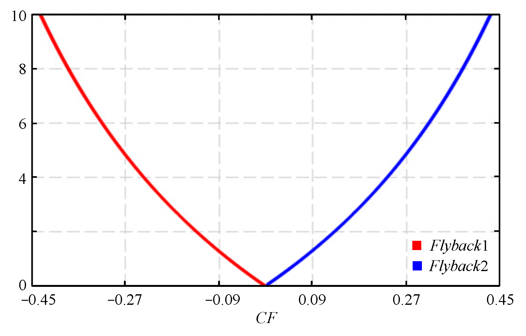
Figure 15 shows the PI module. Multiplying the signal Error by the coefficient kp obtains the proportional control force P, and multiplying the signal Error by the coefficient ki as well as adding this value with the previous integral control force yields the integral control force I. Finally, the control force CF is obtained by summing P and I. When Io1 < Io2, the control force CF will be less than zero, this value is multiplied by −1 to obtain the signal Flyback1_Duty, and the first phase flyback converter will operate. When Io1 > Io2, the control force CF will be greater than zero, the signal Flyback2_Duty is equal to CF, and the second phase flyback converter will operate. After this, a duty limiter is used to limit the maximum duty cycle to 0.45, proceeding to the PWM module. The values of kp and ki are 0.1 and 0.01, respectively.

5.3. PWM Module

In the PWM module, the PWM control will be realized by setting PWM-related registers, which include frequency, duty cycle, phase, blanking time, complementary signal, etc. Therefore, the value of the control force CF is directly fed into the duty cycle-related registers. The half-bridge gate driving signal of the first phase, called vgs1, is generated by PWM1, whereas the half-bridge gate driving signal of the second phase 2, called vgs6, is generated by PWM2. The frequencies of PWM1 and PWM2 are set at 110 kHz, the duty cycle is set to 45% with the prescribed blanking time of 200 ns, and the phase difference between vgs1 and vgs6 is set to 90°. The gate driving signal of phase 1’s flyback converter, called vgs5, is created by PWM3, whereas the gate driving signal of phase 2’s flyback converter, called vgs10, is created by PWM4. The frequencies of PWM3 and PWM4 are set at 100 kHz.
As shown in Figure 16, the flyback converters of the two phases will not operate simultaneously. Only the phase with insufficient voltage gain will operate, causing the efficiency to be improved to some extent.

6. Experimental Results

Experimental results contain measured waveforms and measured data, which are used to validate the effectiveness of the proposed circuit.

6.1. Measured Waveforms

The following associated experimental waveforms at rated load are shown from Figure 17, Figure 18, Figure 19, Figure 20, Figure 21, Figure 22, Figure 23, Figure 24, Figure 25, Figure 26, Figure 27, Figure 28 and Figure 29.
As can be seen in Figure 17, when the switches S1 and S2 are turned off, the voltages across them are equal to the input voltage Vin.
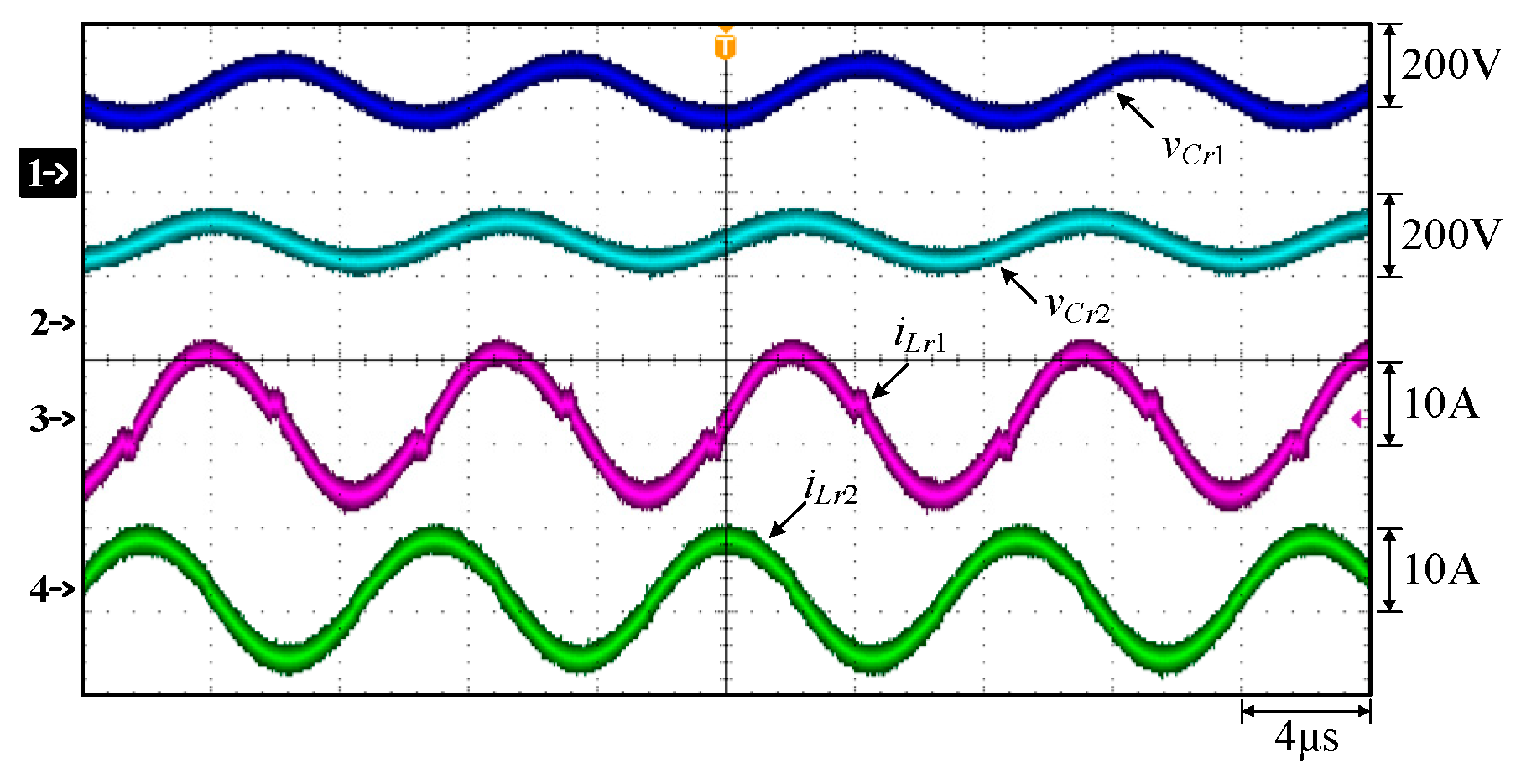
As can be seen in Figure 18, Figure 19, Figure 20 and Figure 21, the duty cycle of the gate driving signal vgs1 for the switch S1 and the gate driving signal vgs2 for the switch S2 are about 45%, and they are complementary signals. The duty cycle of the gate driving signal vgs6 of the switch S6 and the gate driving signal vgs7 of the switch S7 are about 45%, and they are also complementary signals. In addition, the phase difference between vgs1 and vgs6 is 90°. Therefore, the phase difference between the phase 1 resonant inductor current iLr1 and the phase 2 resonant inductor current iLr2 is 90°. According to [34], it can be known that the gate driving signals of vgs3, vgs4, vgs8, and vgs9 will be reduced from 10.9 V to 5 V in order to speed up the switching turn-off time.
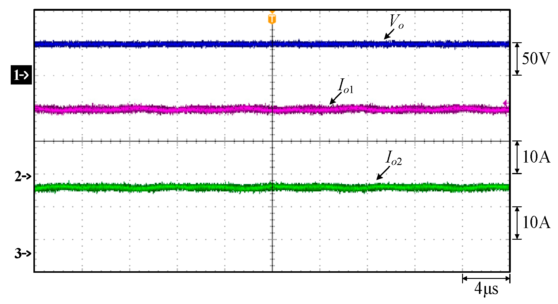
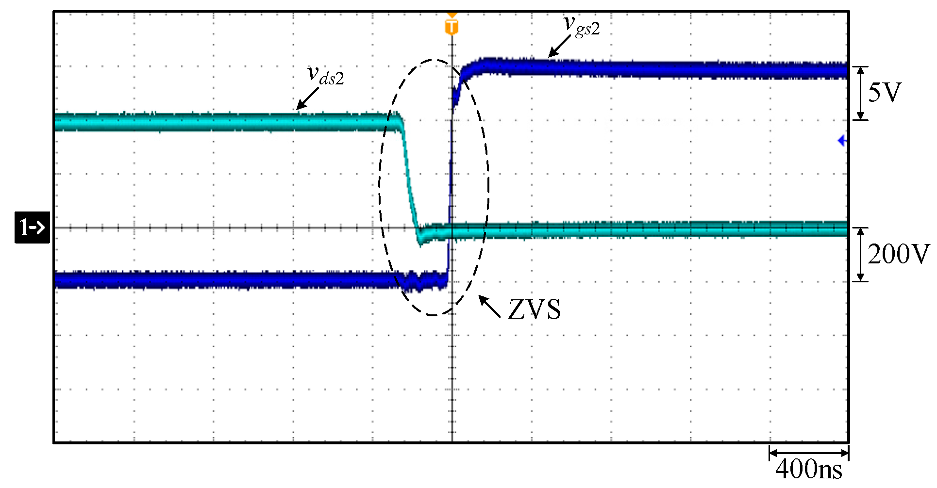
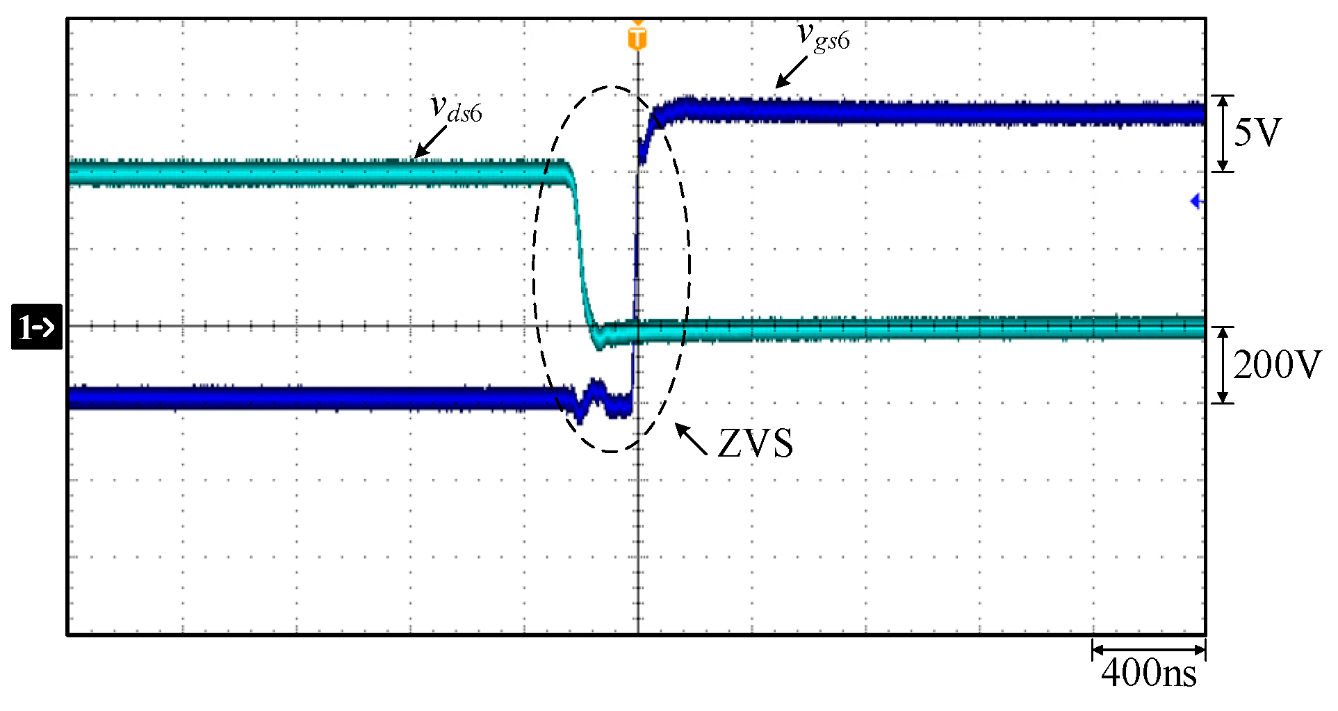
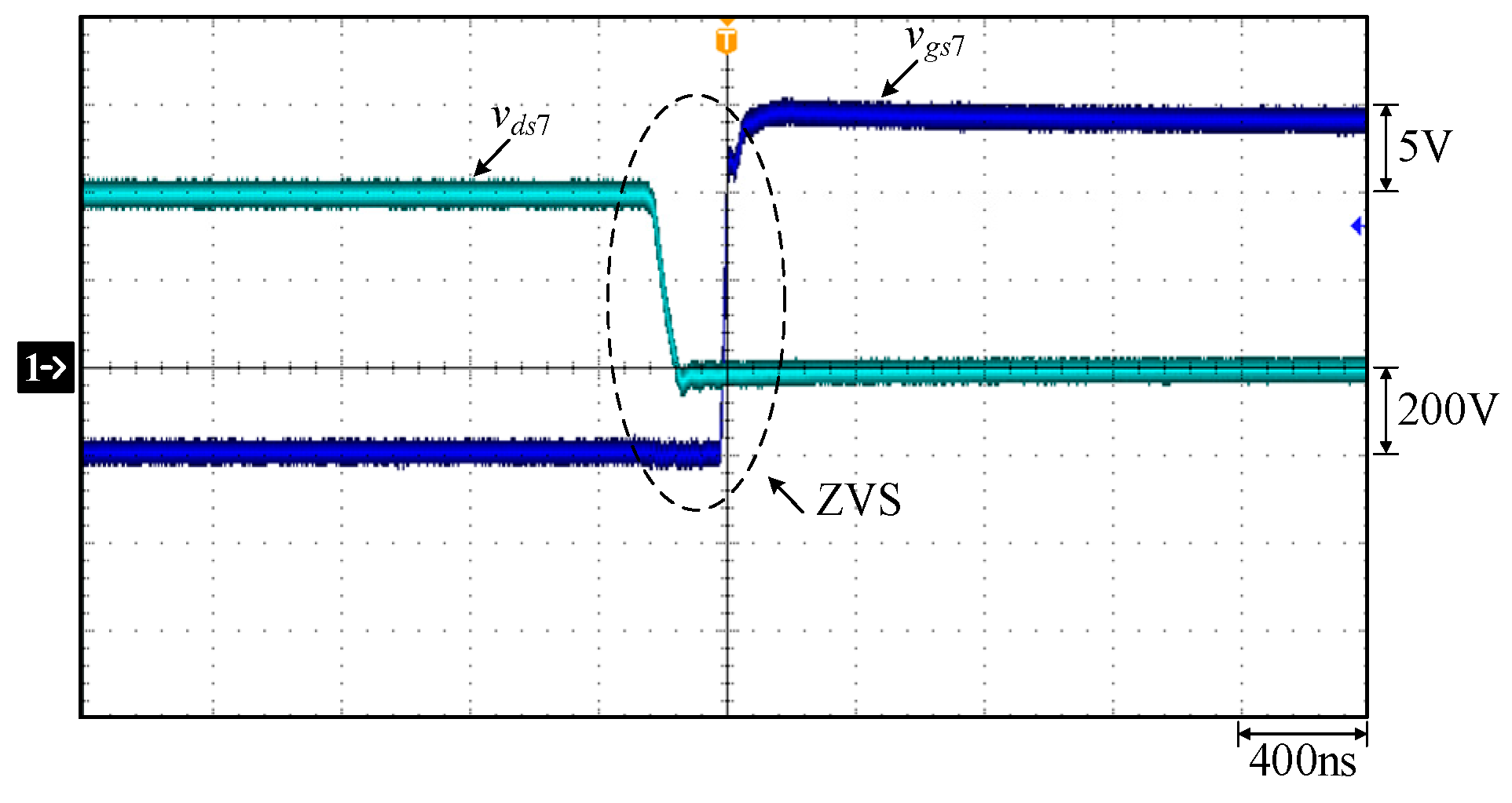
In Figure 22, the output currents of both phases can be equalized. In Figure 23, before the switch S1 is turned on, the voltage across S1 drops to zero, so S1 is turned on with ZVS. In Figure 24, before the switch S2 is turned on, the voltage across S2 drops to zero, so S2 is turned on with ZVS. In Figure 25, before the switch S6 is turned on, the voltage across S6 drops to zero, so S6 is turned on with ZVS. In Figure 26, before the switch S7 is turned on, the voltage across S7 drops to zero, so S7 is turned on with ZVS.
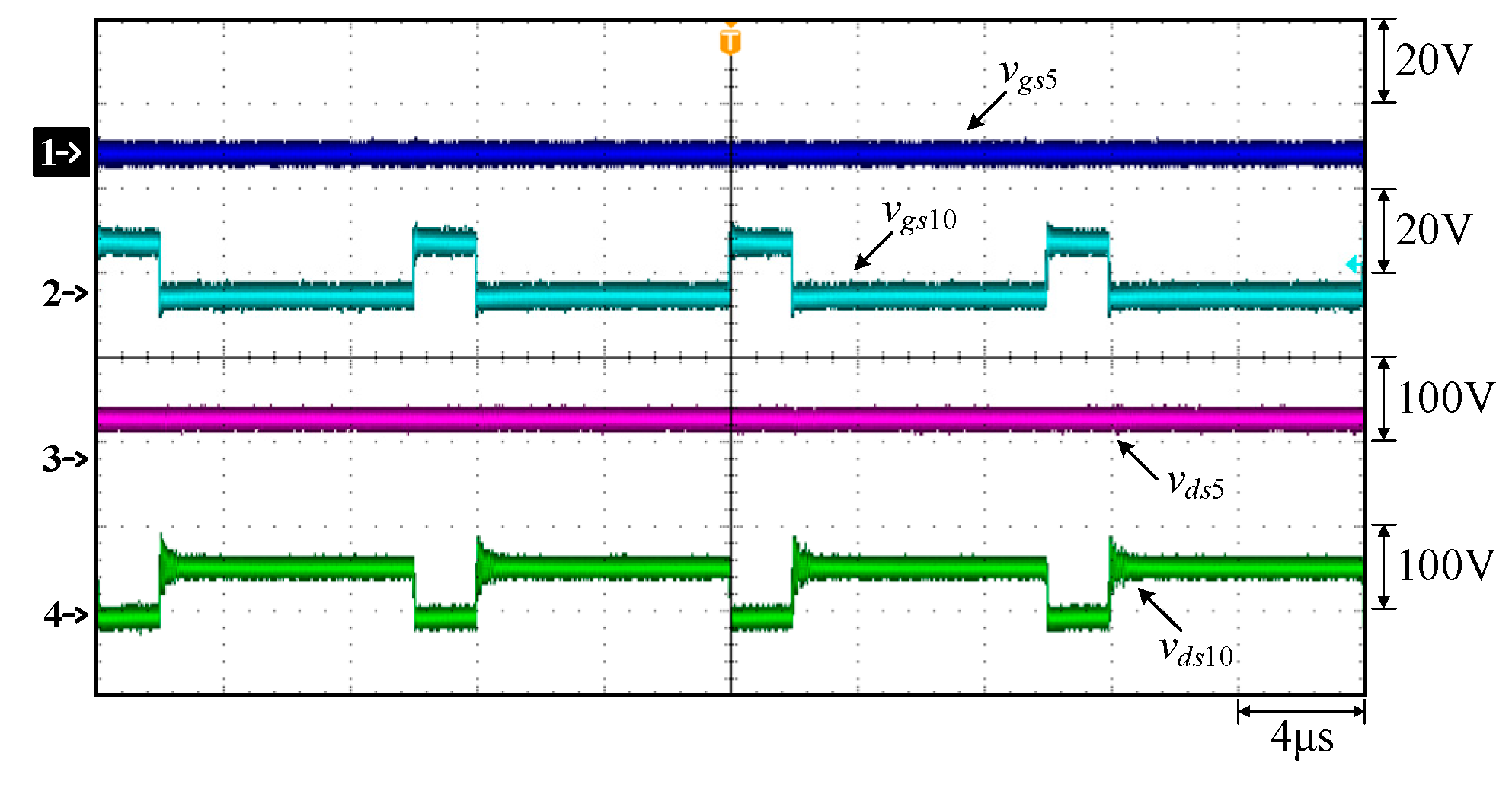
As shown in Figure 27, when the switch S5 is turned off, the voltage across S5 is equal to the input voltage Vin plus the secondary side voltage reflected to the primary side voltage, called nflybackVctrl1. When the switch S10 is turned off, the voltage across S10 is equal to the input voltage Vin plus the secondary side voltage reflected to the primary side voltage, called nflybackVctrl2.
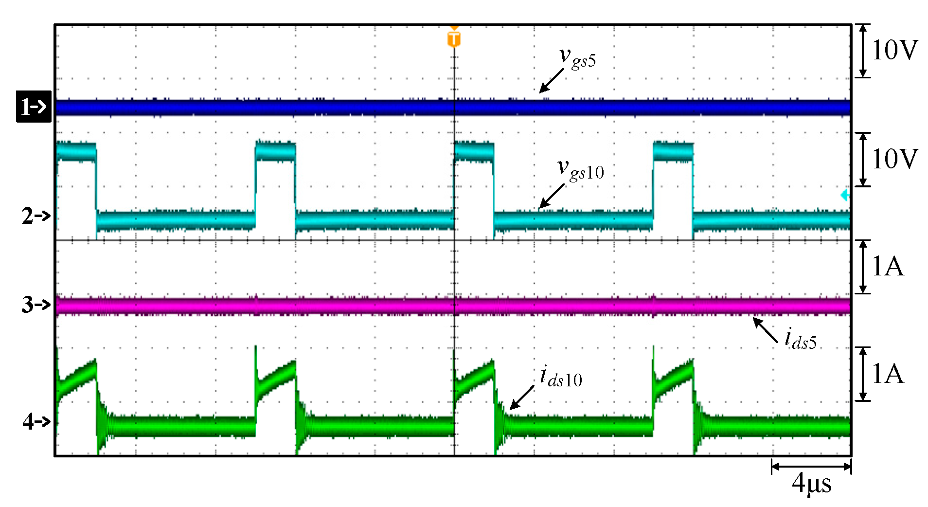
From Figure 28, it can be seen that the switch S5 is turned off, so the current ids5 is equal to zero. However, when the switch S10 is turned on, the current ids10 is not zero, implying that phase 2’s flyback converter is operated in CCM. That is, the two flyback converters do not need to be operated simultaneously. From Figure 29, the negative part of Vctrl1 is due to the forward-biased voltage of the diode, and Vctrl2 is the compensation voltage.

6.2. Measured Data

For efficiency measurement to be considered, one current-sensing resistor is connected in series with the input current path and the other output current-sensing resistor is connected in series with the output current path. Then, the voltage across the current-sensing resistor is measured with a digital meter to obtain the input and output currents, and the input and output voltages are also measured with a digital meter, so as to obtain the input and output power. Finally, the resulting input and output powers are used to calculate the overall efficiency. In addition, the absolute value of the percentage error of the two-phase output currents, called ΔIo, can be defined as follows:
Δ I o = I o 1 I o 2 I o 1 + I o 2 × 100 %
where Io1 is the output current of the first phase, and Io2 is the output current of the second phase.
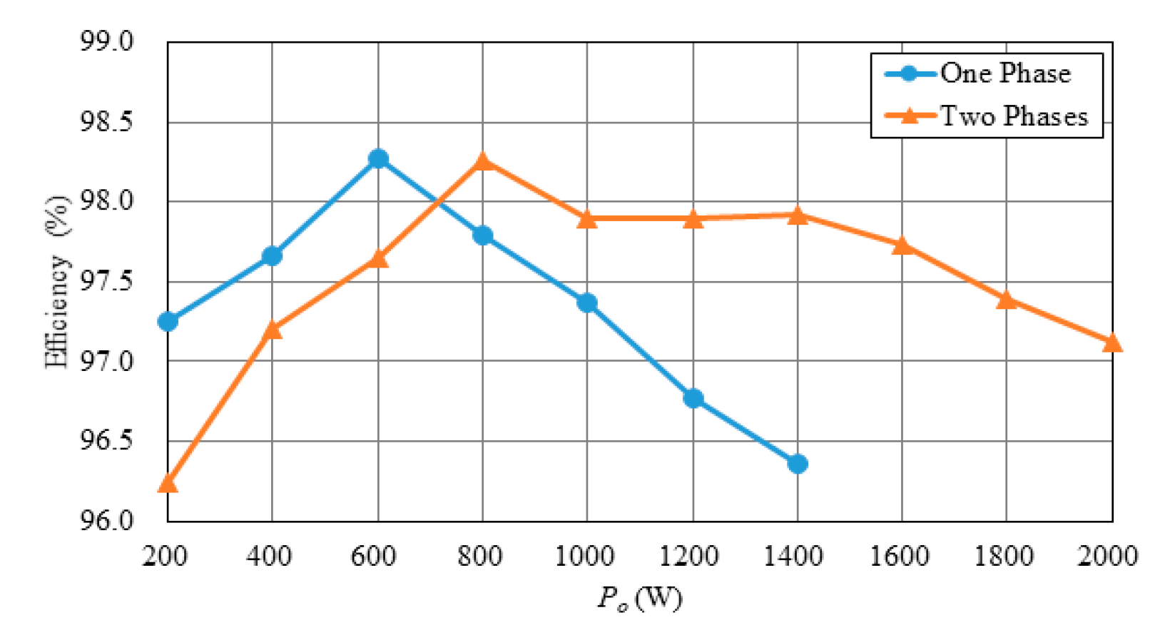
From Figure 30, it can be seen that the efficiency of the two-phase circuit proposed in this paper can be maintained above 96.24% at 10% of the rated power, and the maximum efficiency can reach 98.26%. The maximum efficiency of the single-phase circuit proposed in this paper can reach 98.27%. That is to say, in order to improve the efficiency of the two-phase circuit at the light load, the system can be operated in single-phase circuit by shutting down one of the two phases of the circuit to improve the efficiency at light load. As shown in Figure 31, the light-load efficiency of the two-phase circuit with current sharing control is lower than that without current sharing control because of the increase in the loss caused by the compensation voltage. As shown in Figure 32 and Figure 33, without current sharing control, the output current error percentage is higher than 45% at 10% of the rated power, while with current sharing control, the output current error percentage can be maintained within 3% all over the load range.

6.3. Experimental Setup

Figure 34 shows the photo prototype.

7. Literature Comparison

As shown in Table 3, literature comparison contains seven items: (i) phase shift capability; (ii) phase expansion capability; (iii) additional auxiliary circuit; (iv) additional passive component; (iv) peak efficiency; and (v) current sharing error percentage at rated load.
The circuit in [11] has an output power of 960 W at rated load. The input voltage is 340 V to 400 V, and the output voltage is 48 V. The circuit in [14] has an output power of 600 W at rated load, an input voltage of 400 V, and an output voltage of 12 V. The circuit in [23] has an output power of 1 kW at rated load, an input voltage of 390 V to 410 V, and an output voltage of 54 V. The circuit in [30] has an output power of 1.5 kW at rated load, an input voltage of 350 V to 370 V, and an output voltage of 40 V. The circuit in [31] has an output power of 200 W at rated load, an input voltage of 48 V to 60 V and an output voltage of 5 V. The proposed circuit has an output power of 2 kW at rated load, an input voltage of 400 V, and an output voltage of 48 V.
Table 3 shows that the two-phase circuits in [11,14] must work simultaneously and cannot operate under interleave control, resulting in an inability to minimize the output current ripple. This makes it impossible to improve the efficiency of the system by shutting down one phase of the circuit during light load operation. In [30,31], the current equalization control is carried out by additional auxiliary circuits. The literature [11] achieves current equalization by changing the secondary winding connection, so there is no need for any additional auxiliary circuit and passive component. The literature [14] achieves current equalization by inserting an additional capacitor to the two-phase circuit and using the ampere-second balance of the capacitor. The literature [23] achieves current equalization by controlling the secondary rectifier switch, so there is no need to use any additional auxiliary circuit and passive component to the circuit. Compared to [11,14,23,30,31], the proposed circuit has a relatively high peak efficiency of 98.26%.

8. Discussion

In the following, there are two items to be discussed:
  • In this paper, LLC converter has been designed based on the constant duty cycle and switching frequency near the resonant frequency to obtain better efficiency. At the same time, the value of the K factor is designed to be relatively large to achieve better efficiency, thereby making the voltage gain hard to control.
  • The auxiliary flyback converters are designed only to compensate for the resonant tank component deviation between different phases. If the voltage gain needs to be compensated, the relatively high powers coming from these auxiliary circuits should be afforded.

9. Conclusions

In this paper, a flyback converter is added to an LLC resonant converter, and the input voltage of the LLC resonant converter can be adjusted by controlling the flyback converter in order to balance the output currents of the two phases. Above all, since the required power of the flyback converter is very small compared to the output power and only one phase operates at the same time, the flyback converter has very little effect on the overall efficiency. Since the LLC resonant converter is operated at constant frequency and close to the first resonant frequency, high efficiency can be achieved during circuit operation. Furthermore, the low dependency between the two phases makes it possible to expand the circuit according to the output power required. Without equalization control, the error of the output current of the two phases is more than 45% at 30% of the rated power. However, by adding the proposed equalization control strategy, the output current error between the two phases can be reduced to less than 1% at 30% of rated power, and the efficiency is higher than 97.5% or above at 30% of rated power, with a peak efficiency of 98.26%.
Regarding future work, the following are the potential challenges:
  • How to apply this proposed methodology to the series, parallel, and series-parallel resonant converters.
  • How to reduce magnetic component by integrating the magnetic component of the LLC converter and that of the flyback converter so as to increase the power density.

Author Contributions

Conceptualization, Y.-L.L., H.-H.C. and K.-I.H.; methodology, Y.-L.L., H.-H.C. and K.-I.H.; software, H.-H.C. and Y.-L.L.; validation, H.-H.C. and Y.-L.L.; formal analysis, H.-H.C.; investigation, H.-H.C.; resources, Y.-L.L.; data curation, H.-H.C.; writing—original draft preparation, K.-I.H.; writing—review and editing, K.-I.H.; visualization, Y.-L.L.; supervision, K.-I.H.; project administration, K.-I.H.; funding acquisition, K.-I.H. All authors have read and agreed to the published version of the manuscript.

Funding

This research was funded by the Ministry of Science and Technology, Taiwan (Grant Number: NSTC 112-2221-E-027-015-MY2).

Data Availability Statement

No new data were created or analyzed in this study. Data sharing is not applicable to this article.

Conflicts of Interest

Author Yue-Lin Lee was employed by Delta Electronics, Inc. Author Han-Hsiang Chen was employed by Monolithic Power Systems (MPS). The remaining authors declare that the research was conducted in the absence of any commercial or financial relationships that could be construed as potential conflicts of interest.

References

  1. Gadelrab, R.; Nabih, A.; Lee, F.C.; Li, Q. LLC resonant converter with 99% efficiency for data center server. In Proceedings of the IEEE Applied Power Electronics Conference and Exposition (APEC), Phoenix, AZ, USA, 14–17 June 2021; pp. 310–319. [Google Scholar]
  2. Yeaman, P. Datacenter Power Delivery Architectures: Efficiency and Annual Operating Costs. Vicor. 2007. Available online: https://www.semanticscholar.org/paper/Datacenter-Power-Delivery-Architectures-%3A-and-Costs-Yeaman/4dfbd26051ce6043c3fd78e4674f73052d219578 (accessed on 11 January 2023).
  3. IEC60335-1 (Safety Extra Low Voltage, SELV). 2012. Available online: https://std.iec.ch/terms/terms.nsf/0/DEC6487A319AA228C1257AA7004FD87D?OpenDocument (accessed on 15 January 2023).
  4. Ahmed, M.H.; Lee, F.C.; Li, Q. LLC converter with integrated magnetics application for 48V rack architecture in future data centers. In Proceedings of the IEEE Conference on Power Electronics and Renewable Energy (CPERE), Aswan, Egypt, 23–25 October 2019; pp. 437–443. [Google Scholar]
  5. Why Are Power Designs Moving to 48V? Vicor. 2018. Available online: https://www.mouser.com/pdfdocs/Why-are-Power-Designs-Moving-to-48V.pdf (accessed on 20 January 2023).
  6. Luo, S. A review of distributed power systems part I: DC distributed power system. IEEE Aerosp. Electron. Syst. Mag. 2005, 20, 5–16. [Google Scholar] [CrossRef]
  7. Baba, D. Benefits of a Multiphase Buck Converter. Texas Instruments. 2012. Available online: https://www.ti.com/lit/an/slyt449/slyt449.pdf?ts=1652769828584&ref_url=https%253A%252F%252Fwww.google.com%252F (accessed on 25 January 2023).
  8. Wang, H.; Chen, Y.; Qiu, Y.; Fang, P.; Zhang, Y.; Wang, L.; Liu, Y.F.; Afsharian, J.; Yang, Z. Common capacitor multiphase LLC converter with passive current sharing ability. IEEE Trans. Power Electron. 2018, 33, 370–387. [Google Scholar] [CrossRef]
  9. Wang, H.; Chen, Y.; Liu, Y.-F.; Afsharian, J.; Yang, Z. A passive current sharing method with common inductor multiphase LLC resonant converter. IEEE Trans. Power Electron. 2017, 32, 6994–7010. [Google Scholar] [CrossRef]
  10. Wang, H.; Chen, Y.; Liu, Y.F.; Yang, Z.A.; Afsharian, J.; Gong, B. LLC resonant converter with shared power switches and dual coupled resonant tanks to achieve automatic current sharing. In Proceedings of the IEEE Energy Conversion Congress and Exposition (ECCE), Cincinnati, OH, USA, 1–5 October 2017; pp. 5712–5719. [Google Scholar]
  11. Yang, Y.; Yao, J.; Li, H.; Zhao, J. A novel current sharing method by grouping transformer’s secondary windings for a multiphase LLC resonant converter. IEEE Trans. Power Electron. 2020, 35, 4877–4890. [Google Scholar] [CrossRef]
  12. Noah, M.; Endo, S.; Ishibashi, H.; Nanamori, K.; Imaoka, J.; Umetani, K.; Yamamoto, M. A current sharing method utilizing single balancing transformer for a multiphase LLC resonant converter with integrated magnetics. IEEE J. Emerg. Sel. Top. Power Electron. 2018, 6, 977–992. [Google Scholar] [CrossRef]
  13. Ahmad, U.; Cha, H.; Naseem, N. Integrated current balancing transformer based input-parallel output-parallel LLC resonant converter modules. IEEE Trans. Power Electron. 2021, 36, 5278–5289. [Google Scholar] [CrossRef]
  14. Kirshenboim, O.; Peretz, M.M. Combined multilevel and two-phase interleaved LLC converter with enhanced power processing characteristics and natural current sharing. IEEE Trans. Power Electron. 2018, 33, 5613–5620. [Google Scholar] [CrossRef]
  15. Shimada, T. Current sharing method using secondary voltage ripple for an interleaved LLC resonant converter. In Proceedings of the IEEE European Conference on Power Electronics and Applications (ECPEA), Genova, Italy, 3–5 September 2019; pp. 1–7. [Google Scholar]
  16. Nakakohara, Y.; Otake, H.; Evans, T.M.; Yoshida, T.; Tsuruya, M.; Nakahara, K. Three-phase LLC series resonant dc/dc converter using sic mosfets to realize high-voltage and high-frequency operation. IEEE Trans. Ind. Electron. 2016, 63, 2103–2110. [Google Scholar] [CrossRef]
  17. Kim, B.; Park, K.; Kim, C.; Moon, G. Load sharing characteristic of two-phase interleaved LLC resonant converter with parallel and series input structure. In Proceedings of the IEEE Energy Conversion Congress and Exposition (ECCE), San Jose, CA, USA, 20–24 September 2009; pp. 750–753. [Google Scholar]
  18. Yang, G.; Dubus, P.; Sadarnac, D. Double-phase high-efficiency, wide load range high- voltage/low-voltage LLC dc/dc converter for electric/hybrid vehicles. IEEE Trans. Power Electron. 2015, 30, 876–1886. [Google Scholar] [CrossRef]
  19. Murata, K.; Kurokawa, F. An interleaved PFM LLC resonant converter with phase-shift compensation. IEEE Trans. Power Electron. 2016, 31, 2264–2272. [Google Scholar] [CrossRef]
  20. Two-Phase Interleaved LLC Resonant Converter Design with C2000TM Microcontrollers. Texas Instruments. 2020. Available online: https://www.ti.com/lit/ug/tiduct9a/tiduct9a.pdf?ts=1652705048373&ref_url=https%253A%252F%252Fwww.ti.com%252Ftool%252FTIDM-1001 (accessed on 20 April 2023).
  21. Jang, Y.; Jovanovic, M.M.; Ruiz, J.; Kumar, M.M.; Liu, G. A novel active-current-sharing method for interleaved resonant converters. In Proceedings of the IEEE Applied Power Electronics Conference and Exposition (APEC), Charlotte, NC, USA, 15–19 March 2015; pp. 1461–1466. [Google Scholar]
  22. Sun, J.; Tang, X.; Xing, Y.; Chen, B.; Wu, H.; Sun, K. Current sharing control of interleaved LLC resonant converter with hybrid rectifier. In Proceedings of the IEEE Applied Power Electronics Conference and Exposition (APEC), Anaheim, CA, USA, 17–21 March 2019; pp. 2223–2227. [Google Scholar]
  23. Sato, M.; Takiguchi, R.; Imaoka, J.; Shoyama, M. A novel secondary PWM-controlled interleaved LLC resonant converter for load current sharing. In Proceedings of the IEEE International Power Electronics and Motion Control Conference (IPEMCC), Hefei, China, 22–26 May 2016; pp. 2276–2280. [Google Scholar]
  24. Chen, H.; Jiang, H.; Ren, G.; Du, P.; Shao, S. A secondary partial energy phase shift regulation LLC resonant converter with current sharing ability. In Proceedings of the IEEE International Conference on Power Electronics and ECCE Asia (ICPE & ECCE Asia), Busan, Republic of Korea, 27–30 May 2019; pp. 1141–1146. [Google Scholar]
  25. Hu, Z.; Qiu, Y.; Wang, L.; Liu, Y. An interleaved LLC resonant converter operating at constant switching frequency. IEEE Trans. Power Electron. 2014, 29, 2931–2943. [Google Scholar] [CrossRef]
  26. Hu, Z.; Qiu, Y.; Liu, Y.-F.; Sen, P.C. A control strategy and design method for interleaved LLC converters operating at variable switching frequency. IEEE Trans. Power Electron. 2014, 29, 4426–4437. [Google Scholar] [CrossRef]
  27. Orietti, E.; Mattavelli, P.; Spiazzi, G.; Adragna, C.; Gattavari, G. Two-phase interleaved LLC resonant converter with current-controlled inductor. In Proceedings of the IEEE Brazilian Power Electronics Conference (BPEC), Bonito-Mato Grosso do Sul, Brazil, 27 September–1 October 2009; pp. 298–304. [Google Scholar]
  28. Liu, F.; Zhou, G.; Ruan, X.; Ji, S.; Zhao, Q.; Zhang, X. An input-series-output-parallel converter system exhibiting natural input-voltage sharing and output-current sharing. IEEE Trans. Ind. Electron. 2021, 68, 1166–1177. [Google Scholar] [CrossRef]
  29. Chen, H.; Wu, X.; Shao, S. A current-sharing method for interleaved high-frequency LLC converter with partial energy processing. IEEE Trans. Ind. Electron. 2020, 67, 1498–1507. [Google Scholar] [CrossRef]
  30. Wang, M.; Zha, X.; Pan, S.; Gong, J.; Lin, W. A current-sharing method for interleaved high-frequency LLC converter with partial energy phase shift regulation. IEEE J. Emerg. Sel. Top. Power Electron. 2022, 10, 760–772. [Google Scholar] [CrossRef]
  31. Zhang, F.; Ma, Y.; Lu, H.; Cai, R.; Zhao, Z. Research on current sharing method of two-phase parallel sigma converter. In Proceedings of the IEEE Energy Conversion Congress & Exposition-Asia (ECCE-Asia), Singapore, 24–27 May 2021; pp. 379–384. [Google Scholar]
  32. Classification and Characterization of Various Inductors. Richtek. 2017. Available online: https://www.richtek.com/Design%20Support/Technical%20Document/~/media/AN%20PDF/AN053_TW.ashx (accessed on 30 April 2023).
  33. Scire, D.; Lullo, G.; Vitale, G. EMI filter re-design in a SMPS with inductor in saturation. In Proceedings of the 2021 IEEE 15th International Conference on Compatibility, Power Electronics and Power Engineering (CPE-POWERENG), Florence, Italy, 14–16 July 2021; pp. 1–7. [Google Scholar]
  34. Scirè, D.; Lullo, G.; Vitale, G. Assessment of the current for a non-linear power inductor including temperature in DC-DC converters. Electronics 2023, 12, 579. [Google Scholar] [CrossRef]
  35. Bayoumi, E.H.E. Design of three-phase LCL filter for grid-connected PWM inverter using hybrid bacteria foraging-particle swarm optimization. Int. J. Power Electron. 2012, 4, 497–504. [Google Scholar]
  36. Dinwoodie, L. Design Review: Isolated 50 Watt Flyback Converter Using the UCC3809 Primary Side Controller and the UC3965 Precision Reference and Error Amplifier; Texas Instruments: Dallas, TX, USA, 1999. [Google Scholar]
Figure 1. Traditional power supply structure.
Energies 17 03859 g001
Figure 2. The power supply structure for Google 48 V [4].
Energies 17 03859 g002
Figure 3. Current sharing strategies.
Energies 17 03859 g003
Figure 4. Proposed single-phase LLC resonant converter with partial energy processing.
Energies 17 03859 g004
Figure 5. Proposed two-phase LLC resonant converter with partial energy processing.
Energies 17 03859 g005
Figure 6. Equivalent circuit of the LLC resonant converter.
Energies 17 03859 g006
Figure 7. Equivalent circuit of the LLC resonant converter in the s-domain.
Energies 17 03859 g007
Figure 8. Voltage gain curves of the two-phase LLC converter.
Energies 17 03859 g008
Figure 9. Equivalent circuit of the proposed circuit.
Energies 17 03859 g009
Figure 10. Voltage-dependent source.
Energies 17 03859 g010
Figure 11. Voltage gain of the proposed two-phase LLC converter.
Energies 17 03859 g011
Figure 12. Extension of the phase account for the proposed circuit.
Energies 17 03859 g012
Figure 13. Main program flow chart.
Energies 17 03859 g013
Figure 14. ADC sampling triggering and data calculation.
Energies 17 03859 g014
Figure 15. The PI module.
Energies 17 03859 g015
Figure 16. Curve of Vctrl versus CF for the two flyback converters.
Energies 17 03859 g016
Figure 17. Measured waveforms: (1) vgs1; (2) vgs6; (3) vds1; (4) vds6.
Energies 17 03859 g017
Figure 18. Measured waveforms: (1) vgs1; (2) vgs6; (3) iLr1; (4) iLr2.
Energies 17 03859 g018
Figure 19. Measured waveforms: (1) vCr1; (2) vCr2; (3) iLr1; (4) iLr2.
Energies 17 03859 g019
Figure 20. Measured waveforms: (1) vgs1; (2) vgs2; (3) vgs3; (4) vgs4.
Energies 17 03859 g020
Figure 21. Measured waveforms: (1) vgs6; (2) vgs7; (3) vgs8; (4) vgs9.
Energies 17 03859 g021
Figure 22. Measured waveforms: (1) Vo; (2) Io1; (3) Io2.
Energies 17 03859 g022
Figure 23. Measured waveforms: (1) vgs1 and vds1.
Energies 17 03859 g023
Figure 24. Measured waveforms: (1) vgs2 and vds2.
Energies 17 03859 g024
Figure 25. Measured waveforms: (1) vgs6 and vds6.
Energies 17 03859 g025
Figure 26. Measured waveforms: (1) vgs7 and vds7.
Energies 17 03859 g026
Figure 27. Measured waveforms: (1) vgs5; (2) vgs10; (3) vds5; (4) vds10.
Energies 17 03859 g027
Figure 28. Measured waveforms: (1) vgs5; (2) vgs10; (3) ids5; (4) ids10.
Energies 17 03859 g028
Figure 29. Measured waveforms: (1) Vctrl1 and (2) Vctrl2.
Energies 17 03859 g029
Figure 30. Curves of efficiency versus load power for single-phase and two-phase circuits.
Energies 17 03859 g030
Figure 31. Curves of efficiency versus load power for two-phase circuit with and without current sharing control.
Energies 17 03859 g031
Figure 32. Curve of output current error percentage versus load power without current sharing control.
Energies 17 03859 g032
Figure 33. Curve of the percentage error of output current versus load power with current sharing control.
Energies 17 03859 g033
Figure 34. Photo of the experimental setup.
Energies 17 03859 g034
Table 1. Specifications of the single-phase LLC resonant converter.
SpecificationValue
Rated input voltage (Vdc)400 V
Rated output voltage (Vo)48 V
Rated output current (Io1,rated)21 A
Switching frequency (fs1)110 kHz
Resonant frequency (fr1)120 kHz
Ratio of magnetizing inductance to resonant inductance (K)20
Quality factor (Q)0.2
Table 2. Specifications of the flyback converter.
SpecificationValue
Rated input voltage (Vo)48 V
Maximum dependent voltage (Vctrl,max)10 V
Output maximum current (Iin1,max)2.7 A
Output minimum current (Iin1,min)1 A
Switching frequency (fs2)100 kHz
Table 3. Comparison of the proposed current equalization strategy with the related literature.
Reference [11][14][23][30][31]Proposed
Item
Phase Shift CapabilityNoNoYesYesYesYes
Phase Expansion
Capability
NoNoYesYesYesYes
Additional Auxiliary
Circuit
NoNoNoYesYesYes
Additional Passive
Component
NoYesNoNoNoNo
Peak Efficiency97.5%97.3%None96.8%97.1%98.26%
Current Sharing
Error Percentage
(at rated load)
0.5%0.55%None4.8%1%1.27%
Disclaimer/Publisher’s Note: The statements, opinions and data contained in all publications are solely those of the individual author(s) and contributor(s) and not of MDPI and/or the editor(s). MDPI and/or the editor(s) disclaim responsibility for any injury to people or property resulting from any ideas, methods, instructions or products referred to in the content.