Abstract
Wireless power and data transmission (WPDT) solutions for medical implants are highly desired. However, achieving a high-power transmission efficiency and data rate simultaneously over an inductive link remains a significant challenge. This paper presents an innovative WPDT circuit that incorporates additional MOSFETs with an inductor in a Class-E power amplifier (PA), achieving amplitude-shift keying (ASK) modulation to address this issue. Firstly, the efficiency of the inductive power transmission link and Class-E PA was analyzed, providing design insights. Then, leveraging the insights, the proposed circuit was designed in such a way that it could effectively switch between two load networks to maintain high transfer efficiency for ASK modulation. Based on the load networks, the relationship between introducing the inductor’s value and the data modulation index (MI) was derived to help achieve the desired high-power transmission efficiency. Additionally, the design and calculation of the proposed circuit are also presented. Finally, the proposed circuit was validated through simulations and experiments, demonstrating a power delivery to a load of 84.1 mW with a power transmission efficiency of 70.8% at a data rate and carrier frequency of 3 Mbps and 16 MHz, respectively. Furthermore, the bit error rate (BER) is less than 10−6 with an MI of 10%.
1. Introduction
Implantable medical devices (IMDs) have demonstrated remarkable potential in diagnosing and treating organ dysfunctions and have obtained significant research and attention [1,2,3,4]. These devices, including cochlear implants [1], pacemakers [2], deep brain stimulators [3], and retinal prostheses [4], rely on wireless power transmission (WPT) for extended operation, as shown in Figure 1. IMD power consumption generally ranges from microwatts to hundreds of milliwatts, depending on the application. For instance, cochlear implants range from 10 to 100 mW, while a pacemaker requires less than 100 μW [5]. Additionally, optimizing power transmission efficiency extends battery life, reducing the need for frequent surgical interventions [6]. These devices also necessitate data communication with varying data rates (e.g., cochlear implants > 1 Mbps, retinal prostheses 2–20 Mbps) [7]. Higher data rates in IMDs support real-time monitoring, richer data collection, and reduced latency [8]. Therefore, ensuring high-power transmission efficiency and data rates is desired for delivering these medical treatments and healthcare services [9,10].

Figure 1.
Implantable medical devices. (a) Cochlear implant. (b) Pacemaker. (c) Deep brain stimulator. (d) Retinal prosthesis.
The inductive power transmission link is extensively employed in IMDs for simultaneous power and data transmission due to its safety, reliability, simplicity, and suitable dimensions [11,12,13]. To improve power transmission efficiency, the Class-E power amplifier (PA) is commonly utilized to drive the inductive power transmission link as it can achieve high transmission efficiencies. For the Class-E PA, each carrier frequency corresponds to an optimal resonance parameter and load, which is referred to as the optimally tuned state. This state facilitates the achievement of zero-voltage switching (ZVS) and zero-voltage-derivative switching (ZVDS), thus significantly enhancing the system’s efficiency [14,15].
The Class-E PA’s two critical parameters determine the transmitter coil’s voltage amplitude: the quality factor (Q) and the input DC voltage. These parameters can be adjusted to achieve data transmission, such as on–off keying (OOK) and amplitude-shift keying (ASK) modulation schemes. Moreover, by changing the Class-E PA’s carrier frequency and phase, the frequency-shift keying (FSK) and phase-shift keying (PSK) modulations can be implemented for data transmission.
Various methods have been reported to enhance power transmission efficiency and data rates. Typically, two pairs of coils are used—one for power and one for data [16,17,18,19]. This setup can boost power transmission efficiency and data rates but may lead to complex circuitry and increased size. Additionally, mutual inductance coupling between coils can cause power interference and a high bit error rate (BER) [7,20]. In contrast, using a single coil for wireless power and data transmission (WPDT) can effectively resolve interference, reduce the BER, and maintain a compact size [21,22,23].
For the single-coil method, several modulation schemes have been proposed to improve the power transmission efficiency and data rates. Despite efforts to address this challenge using modulation methods like OOK [24], FSK [25], and PSK [26], the challenge still persists. For instance, the high bandwidth required for FSK modulation can increase power loss and circuit complexity. Additionally, the power consumption of demodulator circuits for both FSK and PSK can outweigh their advantage [27]. OOK modulation, despite achieving a 100% modulation index (MI) to minimize the BER, has a lower power transmission efficiency compared to other modulation methods [16]. ASK modulation addresses former modulation schemes’ limitations because of its lower power consumption and simpler structure design [20]. Reference [24] introduces an OOK modulation scheme that controls the input voltage to facilitate power and data transmission. However, despite its simplicity, the transmission efficiency of this scheme is limited to 21%. To improve power transmission efficiency, reference [28] presents a switchable tuned network integrated into the Class-E power amplifier (PA) to transmit power and data. This approach involves additional tuned networks and switching devices to achieve ASK modulation. However, introducing extra components, including inductors, capacitors, switching devices, and logic gate drivers, results in a more complex hardware circuit, diminishing the overall system’s transmission efficiency to 42% at a data rate of 1 Mbps. In an attempt to address these challenges, reference [29] adjusts the resonance capacitance of the Class-E PA to achieve ASK modulation, attaining a power transmission efficiency of 64.6%. Nevertheless, this adjustment of resonance capacitance may elevate current harmonic levels, leading to increased reactive loss. Yet, further power transmission efficiency and data rate improvement are desired and an current research challenge.
This paper endeavors to contribute by enhancing the power transmission efficiency and data rates. To do so, first of all, a comprehensive theoretical which highlights low- and high-efficiency regions analysis is presented, providing design insights. Then, leveraging the insights of efficiency regions, an innovative WPDT circuit for IMD is proposed, which achieves ASK modulation with the help of additional MOSFETs and an inductor. The proposed circuit switches between load networks to maintain high transfer efficiency for ASK modulation, enhancing the power transmission efficiency and data rates.
The subsequent sections of this paper are structured as follows: In Section 2, the efficiency analysis and derivation of WPT are depicted. Section 3 demonstrates the proposed architecture, including its analysis, calculation, and design procedure. Simulation and experimental results are shown in Section 4. Finally, Section 5 presents the conclusion.
2. Efficiency Analysis and Derivation of Wireless Power Transmission
Figure 2 illustrates the WPT’s schematic, including the Class-E PA, the inductive power transmission link with the compensation network, and the half-wave rectifier. The link is extensively used in IMDs to transfer power. Class-E PA is commonly employed in WPT to enable the transfer of DC voltage to AC voltage due to its high efficiency performance. The efficiency of the link and Class-E PA plays a significant role in the WPT system. To achieve a high-power transmission efficiency, this section aims to derive and analyze the factors that impact the efficiency of both the inductive power transmission link and the Class-E PA.

Figure 2.
Wireless power transmission schematic.
2.1. Inductive Power Transmission Link Characteristic Analysis
To minimize energy losses, the inductive power transmission link should attain maximum efficiency. However, various factors impact the overall efficiency of the link, such as the quality factor of the transmitter and receiver coils, coupling coefficient, and impedance matching [30,31]. Efficiency analysis and optimization in inductive power transmission links are crucial, especially in applications where energy conservation and minimal losses are paramount. By considering these factors and utilizing the equivalent model, engineers can work toward designing an inductive power transmission link with maximum efficiency.
Figure 3a depicts the inductive power transmission link schematic with series and parallel (SP) compensation, where Cr and Ct are the parallel- and series-compensated capacitors, Lt and Lr are the transmitter and receiver coils, rt denotes the equivalent series resistance (ESR) of the transmitter coil, rr represents the ESR of the receiver coil. To maximize the power transmission efficiency, the receiver and transmitter coils are operated at the resonant frequency [32]. The resonant frequency is calculated as follows.

Figure 3.
Inductive link with SP compensation equivalent circuit. (a) Inductive link. (b) Receiver equivalent circuit. (c) Transformer model. (d) Inductive link equivalent circuit.
The power transmission efficiency of the inductive power transmission link is directly related to the mutual inductor between the receiver and transmitter coils, as well as their quality factors [32]. The quality factors of the receiver and transmitter coils are defined as Qt = ω0Lt/rt and Qr = ω0Lr/rr, respectively, where ω0 = 2πfr. Considering Qr2 >> 1, the receiver circuit in Figure 3a (indicated by the green, dashed box) can be simplified to the circuit illustrated in Figure 3b. Specifically, the parallel resistance of Figure 3b is defined as Rp = Qr2rr.
Based on Figure 3b, the efficiency of the receiver coil, ηr, is calculated as follows:
where RL is the AC load resistance.
To facilitate the analysis, the inductive link can be regarded as a loosely coupled transformer model. Hence, Figure 3a can be converted into the transformer model depicted in Figure 3c. In Figure 3c, L1 refers to the transformer’s leakage inductance, LM represents the magnetic inductance, and n indicates the turn ratio. Their expressions are depicted as follows:
where k is the coupling coefficient. In the loosely coupled transformer model, the value of k2 is considerably below one [33].
The receiver circuit needs to be reflected in the transmitter circuit to facilitate calculation, as illustrated in Figure 3d. When the receiver operates at its resonant frequency, the reflected resistance Rref is expressed as follows.
According to Equations (2) and (5), the overall power transmission efficiency of the inductive power transmission link, ηIPL, is calculated as follows.
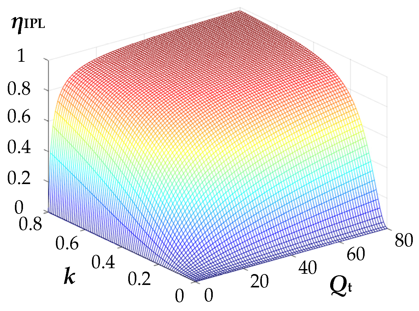
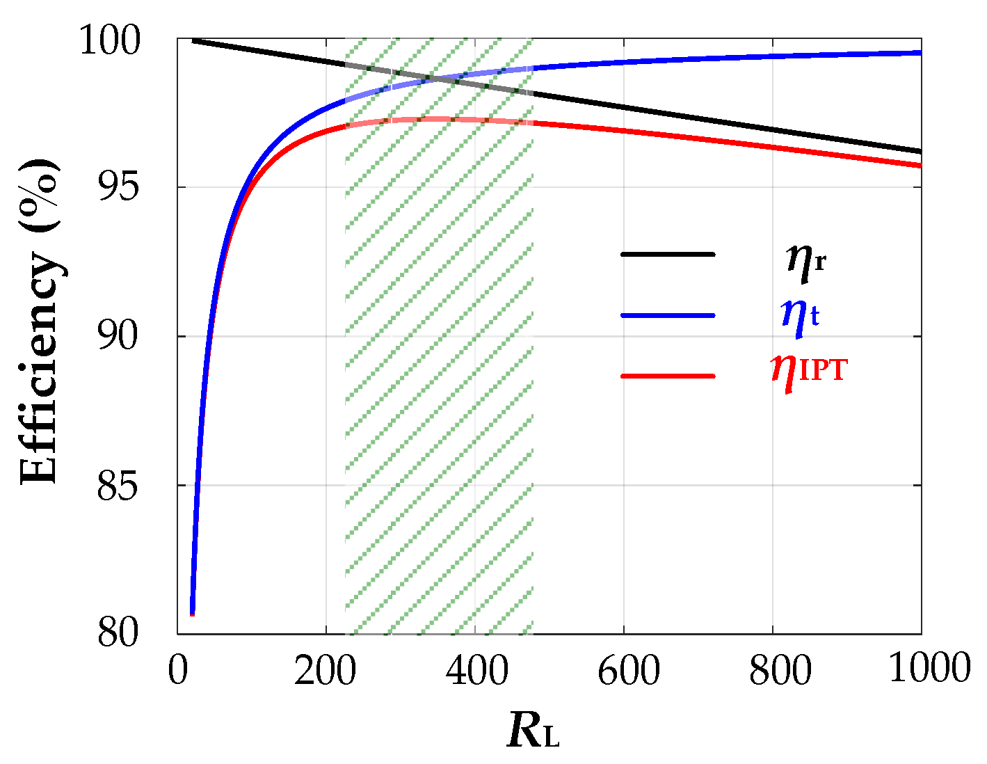
Figure 4 shows the inductive power transmission link’s total efficiency ηIPT changing trend with different k and Qt values. It is evident that the larger values of k and Qt are beneficial for improving the power transmission efficiency of the inductive power transmission link. Moreover, the efficiency of ηIPT is also enhanced as Qr increases. These trends indicate that a stronger coupling and higher quality factor lead to better overall efficiency in WPT. Figure 5 illustrates the changing trends of the efficiencies ηr, ηt, and ηIPT with different RL values. As the RL increases, the receiver efficiency ηr decreases, while the transmitter efficiency ηt exhibits an increasing trend. The inductive power transmission link system’s overall efficiency reaches its maximum efficiency at an optimal RL value range, as highlighted in the green shaded region of Figure 5.
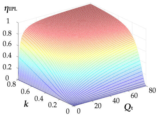
Figure 4.
Changing trend of the inductive power transmission link’s efficiency with different k and Qt.
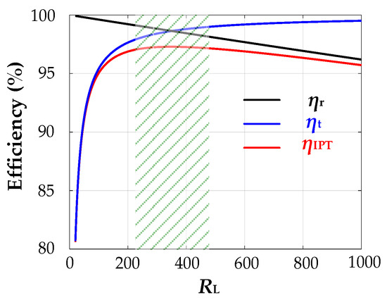
Figure 5.
Changing trend of ηr, ηt, and ηIPT with different RL.
When applied in cochlear implants, permanent magnets are employed to ensure a fixed position between the receiver and transmitter coils. Thus, the value of k between the two coils remains unchanged. Additionally, the k is less than 0.5 in the loosely coupled transformer [33]. Consequently, a more effective method for improving the power transmission efficiency of the inductive power transmission link is to adjust the quality factor of the two coils. However, a higher quality factor may result in a lower bandwidth of data transmission, which does not facilitate the high data rate design target. Consequently, there is a trade-off between high efficiency and high data rate.
2.2. Class-E Power Amplifier Characteristic Analysis
The Class-E PA is usually employed to drive the inductive power transmission link. The Class-E PA’s schematic with the reflected resistance of the receiver circuit is demonstrated in Figure 6, where the Lf acts as the choke inductor, S1 is the MOSFET, Cp denotes the shunt capacitor, and L1-Ct-Req represents the tuned network. The switching frequency of S1 is equal to the inductive power transmission link’s resonant frequency in the Class-E PA.
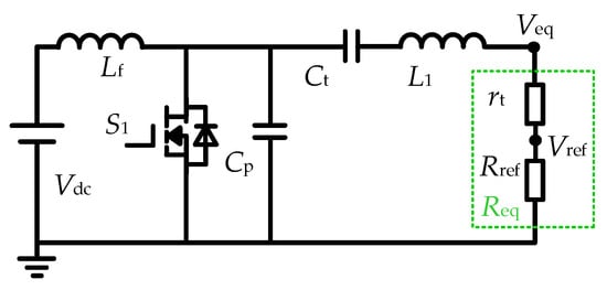
Figure 6.
Schematic of the Class-E PA.
It is widely recognized that the Class-E PA’s high efficiency performance when it satisfies the characteristics of ZVDS and ZVS [34]. However, the Class-E PA exhibits high sensitivity to load variations in this operating state, requiring a specific set value of the L1-Ct-Req-Cp network to match. To address this challenge, the concept of the load angle φ is introduced, which quantifies the variation in the L1-Ct-Req network branch. The expression for load angle φ is calculated by Equation (8).
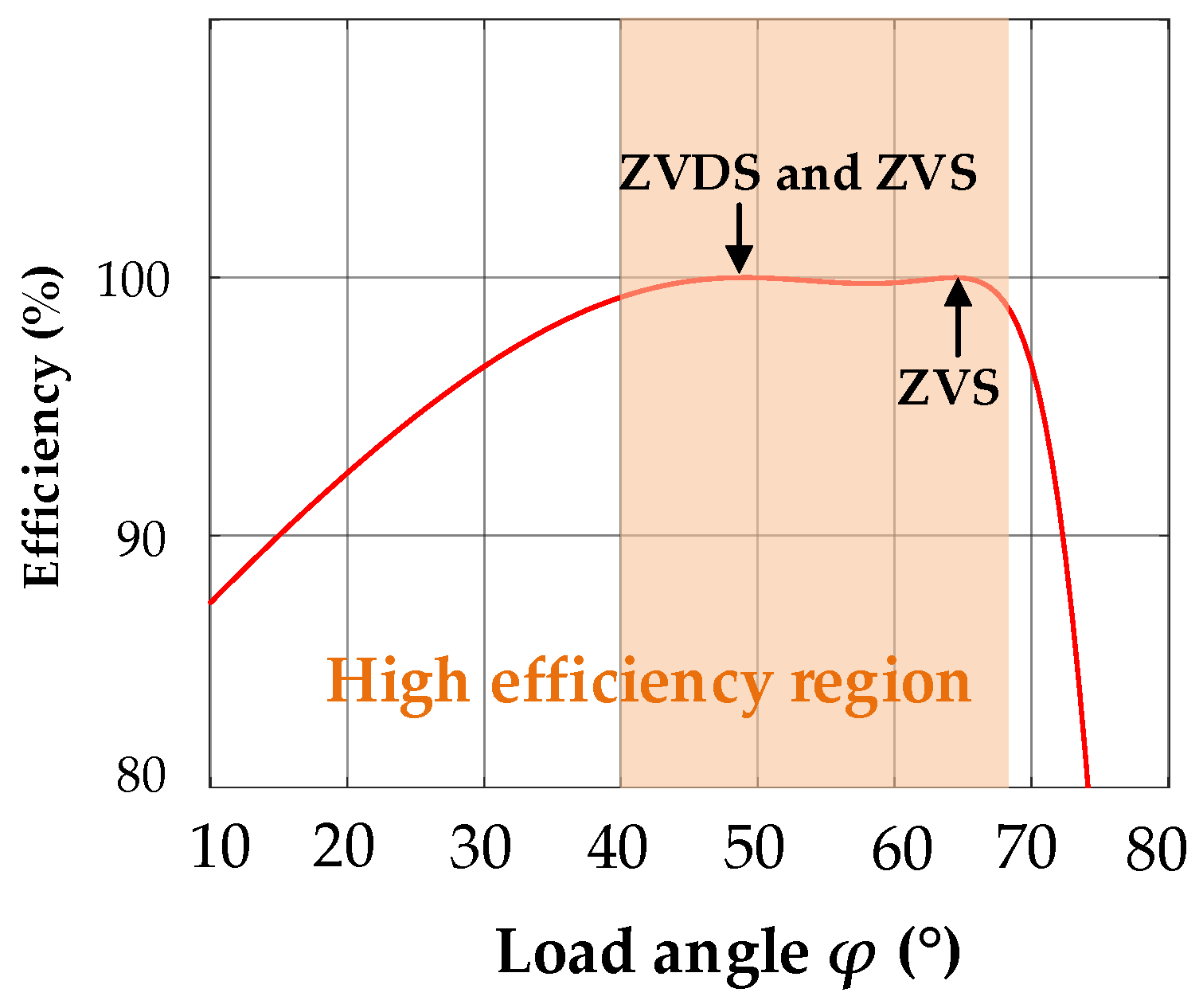
The efficiency of the Class-E PA by sweep load angle φ is shown in Figure 7. It indicates that the efficiency can reach 1 when the φ is about 49°, which corresponds to the optimally tuned state for the Class-E PA. In this state, both the ZVS and ZVDS characteristics are satisfied, and the optimal values of Cp and Ct can be obtained by Equation (9) [35]. On the other hand, the efficiency is close to 1 when the φ is about 64.5°, and the ZVS characteristics are satisfied.
where QL denotes the load quality factor of Class-E PA, which is equal to ω0L1/Req.
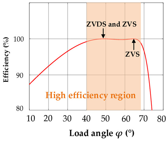
Figure 7.
Class-E PA efficiency with different φ.
In Figure 7, it is valuable to note that the Class-E PA’s efficiency is near its peak in the range of φ from 40° to 67°, which is referred to as the high-efficiency region [36]. This region represents a range of load angles where the Class-E PA operates with high efficiency, even if it is not precisely at the optimal tuning point. In addition, the voltage Vref also follows φ variation. This beneficial phenomenon can be utilized to achieve ASK modulation for transmitting data with high-power transmission efficiency.
According to Equation (8), it is feasible to change φ by adjusting the values of Req, Ct, and L1 for data transmission. However, introducing an additional resistor to alter φ will degrade the system’s efficiency, which is undesirable. Compared to changing the value of Ct, increasing L1 can reduce the reactive power to improve the system’s efficiency further. Consequently, adding an extra inductor can enhance the system’s efficiency and achieve data transmission.
3. Proposed Circuit with ASK Modulation
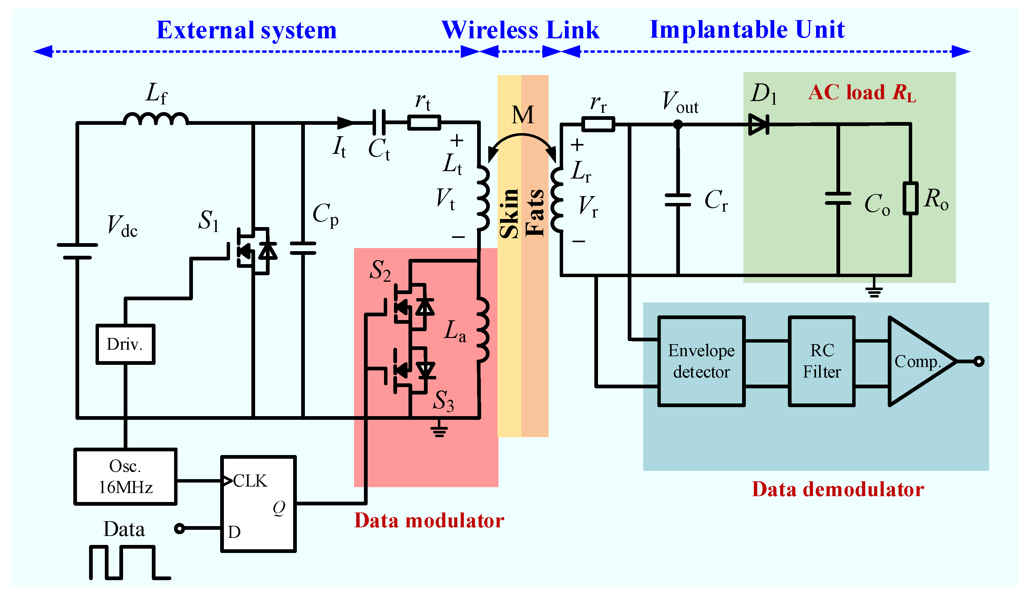
Based on the analysis presented in Section 2, the proposed circuit in this study for WPDT with ASK modulation is illustrated in Figure 8. The proposed circuit extends upon the foundation of Figure 2 by incorporating separate components for data modulation and demodulation (represented by the orange and blue dashed boxes, respectively). Additionally, the green dashed box can be regarded as the AC load RL. The data modulation process involves the switching devices S2 and S3, as well as inductor La. On the other hand, the data demodulation stage comprises the envelope detector, an RC filter, and a comparator. The circuit operation principle is illustrated below.
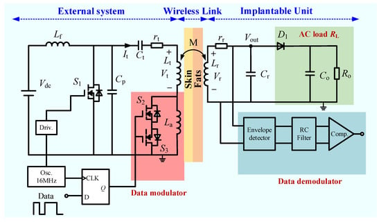
Figure 8.
Schematic of the proposed WPDT circuit.
3.1. Operation Principle
To achieve a high data rate, utilizing a relatively high carrier frequency to extend the bandwidth for data transmission is vital. Meanwhile, it should be noted that the chosen carrier frequency needs to meet human safety requirements (<20 MHz). Therefore, this proposed circuit employs a 16 MHz carrier frequency to drive the Class-E PA. A 16 MHz active crystal oscillator with a fixed duty cycle of 0.5 is utilized to maintain a stable carrier signal. Simultaneously, the input data signal is synchronized with the carrier signal to prevent glitch impulses from occurring at the gate of S1. When the data transmission signal is at a high level, S2 and S3 turn on, enabling the circuit to operate in the Class-E PA’s optimally tuned state. In other words, the Class-E PA has the highest efficiency in this state.
When the data transmission signal is at a low level, S2 and S3 turn off, and La is incorporated into the Class-E PA’s load network, the carrier signal periodically turns S1 on and off. During this time, the load network contains the La and the reactance of the load network is increased, resulting in a reduction in the voltage amplitude of the transmitter coil. As a result, the ASK modulation scheme is achieved. To enhance power transmission efficiency, it is crucial that this load network operates in the high-efficiency region shown in Figure 7. Consequently, this reconstructed load network can be denoted as the Class-E PA’s sub-optimally tuned state.
The purpose of adding S3 is to prevent the flow of AC from the ground to the transmitter coil when the data are at a high level. If S3 is removed, the voltage from the ground to the transmitter coil will exceed 0.7 V, causing the current to flow through the body diode of S2. As a result, achieving ASK modulation becomes challenging due to the slight change in the transmitter’s voltage amplitude.
3.2. Relationship between Vout and φ
To achieve data transmission and maintain high-power transmission efficiency, the relationship between the receiver’s voltage amplitude and the Class-E PA’s load network is crucial. As discussed in Section 2.2, the load angle φ is employed to characterize the properties of the load network. However, up to now, no expression has been reported to elucidate the relationship between Vout and φ within the high-efficiency region. Therefore, this section will delve into their relationship.
The equivalent load, including the Rref and rt, is illustrated in Figure 6. The optimal values about the Cp and Ct at ω0 can be calculated by Equation (9) when the Class-E PA operates at its optimally tuned point. According to [36], the voltage of the equivalent load Req is expressed by Equation (10).
Where the Vdc is the input dc voltage, the dc resistance Rdc and the transfer ratio g of dc-ac voltage are expressed as follows:
where ϕ denotes the load current phase, which is calculated as follows.
Based on Equation (8), the tan(φ) is expressed as follows.
According to Equations (10)–(13), the φ is directly related to Veq. However, if φ is substituted directly into Equation (10), the expression about the relationship between φ and Veq becomes very complicated. Thus, a mathematical fitting method is considered to obtain an equivalent expression. Using a math-fitting tool, the relationship between tan(φ) and Veq_m can be denoted as follows.
The results of the comparison between Veq_m and Veq with different tan(φ) are illustrated in Figure 9, demonstrating excellent agreement. Following insights from Figure 7, the chosen range of φ values were between 40° and 67°, resulting tan(φ) values ranging from 0.8 to 2.4.
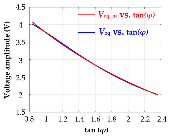
Figure 9.
Comparison of Veq_m and Veq with different tan(φ) values.
According to the turn ratio n, the voltage Vout of the receiver can be calculated as follows.
The Class-E PA enters a sub-optimal state under low data conditions. In this state, an inductor, La is added to the load network. Selecting an appropriate value for La becomes critical in achieving the desired system efficiency, load angle, modulation index, and output voltage amplitude. This choice necessitates a careful trade-off among various performance parameters to ensure effective system operation.
3.3. La Calculation
To ensure high transmission efficiency, high data transmission rates, and low error rates, the choice of La is constrained by the range of φ and MI. The calculation procedure of La is given below based on these two restriction requirements.
In ASK modulation, the MI of the output voltage is defined as follows.
The receiver coil’s output voltage amplitudes are denoted by Vout_H and Vout_L, which corresponds to high-level data and low level data, respectively.
According to the above discussion, the optimally tuned point for Class-E PA is defined when the data are at a high level. Assuming the load angle is φ1 in this state, φ1 is approximately 49° in the optimally tuned state. By inserting the value of φ1 into (14), the voltage of Req is obtained as follows:
By substituting Equation (17) into Equation (15), the Vout_H is:
When the data are low-level, the inductor La is added to the Class-E PA’s load network, and the load angle is assumed to be φa. Using Equation (13), the tan(φa) is given as follows:
By inserting Equations (19) and (14) into Equation (15), the output voltage Vout_L is obtained as follows:
Combining with Equations (16), (18) and (20), the value of La is deduced as below.
The MI is proportional to La’s magnitude. To achieve a low BER, MI should be maximized, favoring schemes like OOK modulation. However, higher MI results in reduced power transmission efficiency. Therefore, for efficient WPDT system transmission, MI is typically set at 10% [29].
3.4. Design Procedure
The power transmission of IMDs, such as cochlear implants, is typically less than 100 mW [22]. Hence, the output power of the IMD in this study is selected to be close to 100 mW. The receiver load Ro is chosen to be 1 kΩ. The RL can be calculated as follows [28].
Where Ro denotes the implant load, Vrec represents the rectifier voltage, and Vdiode refers to the diode’s forward voltage. In this article, the value of the Vdiode is approximately 0.4 V, while Vrec is set at 5 V. Consequently, the RL is about 540 Ω.
The cochlear implant is employed as a demonstration application to validate the research in this article. Based on the proposed coil design in [28], the circular planar spiral coil implemented on PCB emerges as a suitable candidate for WPDT. The values of Lt and Lr are designed to be 3 uH and 1 μH, and their equivalent series resistances rt and rr at 16 MHz are 0.44 Ω and 0.36 Ω, respectively. Additionally, the transmitter and receiver coils turn numbers are eight and five, respectively.
The value of Cr, which resonates with Lr at 16 MHz, was calculated to be 100 pF. Based on the aforementioned, the Class-E PA operates in an optimally tuned state when the data signal is at a high level. Hence, the value of Cp and Ct can be determined using (9) as follows: Cp is calculated to be 29 pF, and Ct is calculated to be 40 pF. Also, the value of Rref is calculated to be 44 Ω using Equation (4).
When the data signal is at a low level, the La is added to the load network. By substituting Req, 10% for MI, and 2π × 16 × 106 for ω0 in (21), La is calculated to be 0.2 μH. According to Equation (19), the value of φ is approximately 55°, which satisfies the constraint requirement of φ.
4. Simulation and Experimental Results
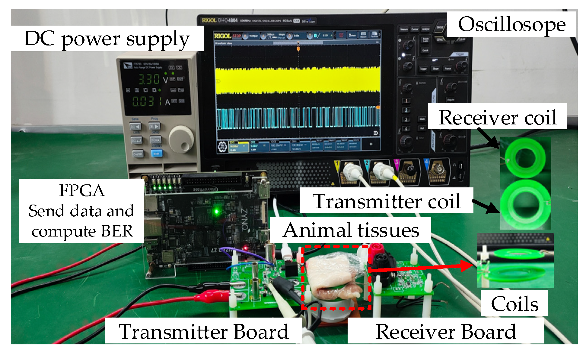
Following the design procedure of the proposed circuit, the performance was evaluated by simulations and experiments. The experimental platform was built as shown in Figure 10. Note that animal tissues are employed as a substitute for human tissues in the experimental testing process.
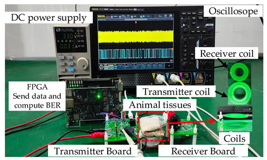
Figure 10.
Experimental platform for the proposed circuit.
4.1. Simulation Results
The simulation circuit is constructed based on the proposed circuit in Figure 8. The circuit parameters are calculated by the aforementioned design procedure. However, the value of Cp obtained from Equation (9) is not accurate enough. The reasons are as follows: for the Class-E PA, achieving its optimal-tuned state is significantly dependent on the values of Cp. The mathematical calculation formula provides only the initial calculation outline. Typically, the value of Cp needs to be adjusted based on its switching waveforms. Therefore, the value of Cp was fine-tuned by a simulation to attain the optimally tuned state. As a result, the value of Cp is determined to be 65 pF. Table 1 lists the circuit parameters.

Table 1.
Parameters of the proposed circuit.
Figure 11 demonstrates the ZVDS and ZVS features during different data conditions. The drain-source voltage (Vd) of S1, the gate-source voltage (Vg) of S1, the resonant current (It), and the drain-source current (Id) of S1 are shown in Figure 11a,b. Figure 11a depicts the waveforms of Vd, Vg, It, and Id when the data signal was at a high level. It is apparent that the S1 satisfies the conditions of ZVDS and ZVS. Similarly, these waveforms are depicted in Figure 11b when the data were at a low level. Clearly, the S1 can achieve ZVS in this state. Additionally, the resonant current waveform exhibits high sinusoidal behavior due to the design of a high load quality factor QL for Class-E PA, reducing the reactive power loss.

Figure 11.
Simulation results of the proposed WPDT circuit. (a) Vd, Vg, It, and Id waveforms when the data signal is at a high level. (b) Vd, Vg, It, and Id waveforms when the data are at a low level. (c) Voltage waveform of the receiver coil when the data rate is 3 Mbps.
Figure 11c illustrates the Vout waveform of the receiver coil when the data rate is 3 Mbps (random bit stream). The voltage amplitudes for high and low data signals (Vout_H = 11.9 V and Vout_L = 9.6 V) closely match the calculated values (Vout_H = 12.1 V and Vout_L = 9.8 V) based on Equations (18) and (20). Similarly, the simulated MI approximates were 10%, which is consistent with the value from Equation (16). This close agreement between simulations and theoretical calculations validates the feasibility of the proposed circuit design methodology.
4.2. Experimental Results
The proposed WPDT with an ASK modulation circuit scheme has been implemented using the experimental platform depicted in Figure 10. The MOSFET selected for the prototype is the BSS138PW from Nexperia, benefiting from its advantageous characteristics, such as a low output capacitance of 7 pF and a small on-resistance of approximately 1.2 Ω. The prototype employs TDK’s C0G capacitors with a capacitance tolerance of 1%. This capacitor material demonstrates outstanding high-frequency characteristics and minimal parameter errors. High-frequency inductors with a self-resonant frequency surpassing 300 MHz have been selected to alleviate the impact of parasitic capacitance. For measurements, a RIGOL oscilloscope with bandwidths of 800 MHz, along with a passive probe with 500 MHz bandwidth, is employed to capture high-frequency signals within the circuit accurately. To minimize measurement errors, the ground wire of the passive probe is substituted with a grounding spring band, ensuring a robust ground connection and enhancing the reliability of measurement data. Additionally, the distance between the transmitter and receiver coils is designed to be 6 mm, considering factors such as the thickness of the body’s skin and fat layers. Detailed and tuned parameters are cataloged in Table 1. Furthermore, the FPGA board is employed in this experimental setup to generate the random data signal and compute the BER.
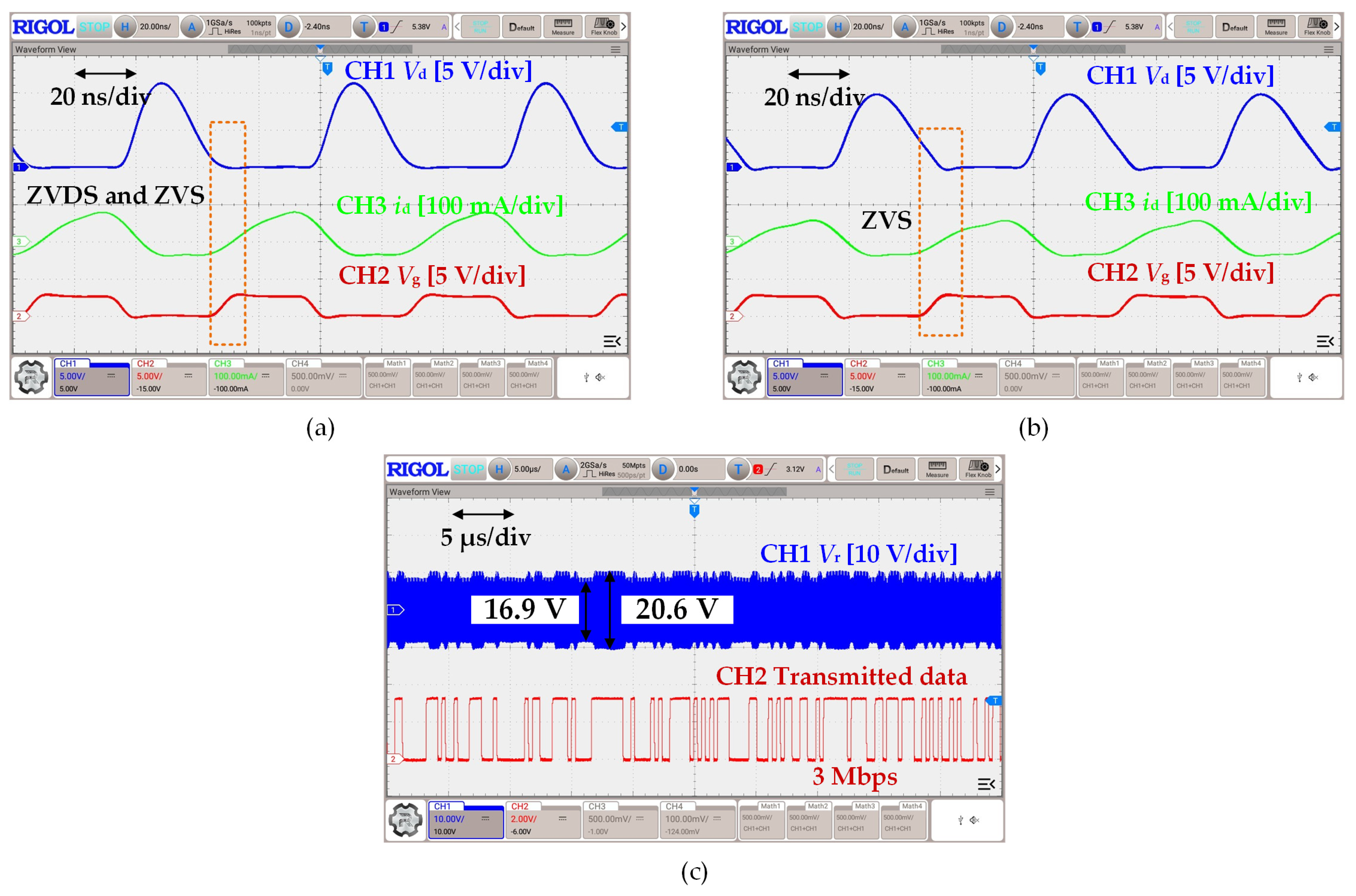
Figure 12 depicts two experimental waveforms of modulation state, showcasing Vd, Vg, and Id. When the data signal was at a high level, the Class-E PA operates in the optimally tuned state, which satisfies the ZVDS and ZVS features, as demonstrated in Figure 12a. The same waveforms for the sub-optimally tuned state when the data signal was at a low level are illustrated in Figure 12b, which satisfies the ZVS conditions.
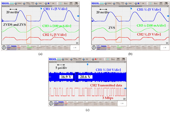
Figure 12.
Experimental results of the proposed WPDT circuit. (a) Vd, Vg, and Id waveforms when the data signal is at a high level. (b) Vd, Vg, and Id waveforms when the data are at a low level. (c) Voltage waveforms of the receiver coil when the data rate is 3 Mbps.
The voltage waveform (Vout) of the receiver coil, operating at a data rate of 3 Mbps, is presented in Figure 12c. When the data signal was high, the voltage amplitude measures approximately 10.3 V, resulting in a transmitted load power of 98.2 mW. In this operational mode, the input power is 125.4 mW, with an estimated power dissipation of around 10 mW from the circuit chips. Consequently, the power transmission efficiency reaches 72.5%. Conversely, when the data signal is low, the voltage amplitude drops to 8.45 V, resulting in a transmitted load power of 66 mW. In this mode, the input power is 85.8 mW, combined with the dissipated power of 10 mW from the circuit chips, thus achieving a power transmission efficiency of 68.9%. The MI for achieving ASK modulation, as indicated by the experimental waveforms, is observed to be approximately 10%, aligning with the theoretical design value.
Compared with the simulation results, the voltage amplitude of the receiver coil is a difference of 1.6 V when the data signal was at a high level, whereas it was a difference of 1.16 V when the data were at a low level. This is because the simulation results are ideal and do not consider the circuit’s ESR. The circuit’s ESR was measured at 16 MHz by an impedance analyzer; the ESR was about 4.8 Ω at a high-level data signal, and the other was about 4.2 Ω. According to the simulation results shown in Figure 11, the transmitter coil current was 95 mA and 76 mA for high-level and low-level data signals, respectively. As a result, the ESR results in a loss of the receiver coil’s voltage amplitude are 1.57 V and 1.1 V. If these error voltages are subtracted from the Vout of the simulation results, the Vout_H is 10.33 V, and the Vout_L is 8.5 V. The Vout results between the simulation and experiment are very close. Therefore, the experimental results verify the feasibility of the proposed circuit design methodology.
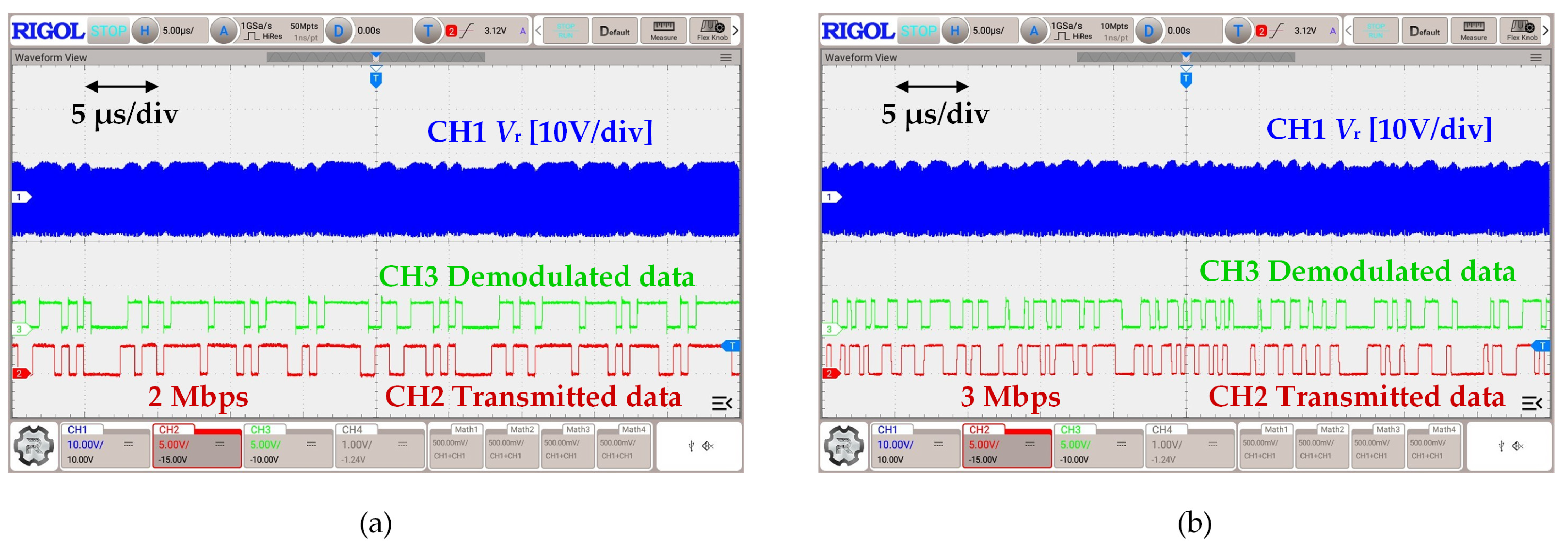
To evaluate the BER, the FPGA transmits several million random bits, which are subsequently captured by the FPGA through the data recovery circuit. After performing computations within the FPGA, it was determined that the BER is less than 10−7 for a data rate of 2 Mbps. Additionally, the measured BER at 3 Mbps is lower than 10−6. Figure 13 illustrates the experimental results for data rates of both 2 Mbps and 3 Mbps, including the receiver coil voltage, the transmitted data, and the demodulated data. It was observed that the demodulated data closely matched the transmitted data.
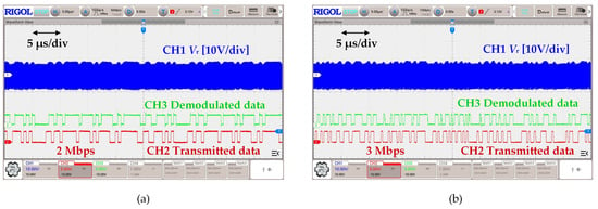
Figure 13.
Measured experimental waveforms with different data rates. (a) 2 Mbps (b) 3 Mbps.
The total power transmission efficiency and output power were investigated at a data rate of 3 Mbps for different distances d between the receiver and transmitter coils. The experimental results are presented in Figure 14. When d = 6 mm, the power transmission efficiency reaches its maximum value due to the Class-E PA being designed for the tuned state. The maximum power transmission efficiency and output power reach 70.8% and 84.1 mW, respectively. As d increases from 6 mm, the coupling coefficient decreases, resulting in a reduction of the induction voltage of the receiver coil and a detuned state for the Class-E PA. Consequently, both power transmission efficiency and output power exhibit a decreasing trend as d increases. Conversely, as d decreases from 6 mm, the coupling coefficient k increases, and the reflected resistance Rref increases. Meanwhile, the Class-E PA also operates in a detuned state. As a result, both power transmission efficiency and output power exhibit a decreasing trend with decreased d.

Figure 14.
Power transmission efficiency and output power under different distances d. (a) Power transmission efficiency with different distances d. (b) Output power with different distances d.
The proposed WPDT circuit has been compared with previous works, and the characteristics of this circuit are outlined in Table 2. The comparison demonstrates that the WPDT developed in this study surpasses the reported circuits in terms of both PTE and data rate.

Table 2.
Comparison with previous works.
In this cochlea implant application, permanent magnets ensure the best coil alignment. However, the coil’s position is prone to change in other IMDs. The system’s power transmission efficiency is sensitive to the coil’s misalignment in other IMDs. Therefore, enhancing the power transmission efficiency in link misalignments can be explored to extend this work for other IMD applications, which has potential for future investigation.
5. Conclusions
In this paper, an innovative circuit for wireless power and data transmission is presented. This circuit incorporates MOSFETs and an inductor into the Class-E PA to adjust the voltage amplitude and enable the ASK modulation scheme for data transmission. The proposed circuit can effectively switch load networks for the ASK modulation scheme to maintain the high-efficiency transmission. Furthermore, the comprehensive parameters design process for the proposed circuit is introduced. Finally, simulations and experiments verify the performance of the proposed circuit. The measured results demonstrate that a power delivery of 84.1 mW can reach a power transmission efficiency of 70.8% at the data rate of 3 Mbps. Moreover, the measured BER is less than 10−6 with a modulation index of 10%. Based on these results, both high data rate and power transmission efficiency targets are successfully achieved.
Author Contributions
H.Z., M.T., X.W. and S.H. developed the idea of this study; H.Z. and M.T. conducted the calculations and experiments; data analysis was performed by H.Z. and M.T.; and X.W. and S.H. revised the manuscript. All authors have read and agreed to the published version of the manuscript.
Funding
This work was supported by the National Natural Science Foundation of China (under Grant 52177199) and the Zhejiang Provincial Natural Science Foundation of China (under Grant LGG22E070013).
Data Availability Statement
Data are contained within the article.
Conflicts of Interest
The authors declare no conflicts of interest.
References
- Henry, F.; Glavin, M.; Jones, E. Noise Reduction in Cochlear Implant Signal Processing: A Review and Recent Developments. IEEE Rev. Biomed. Eng. 2023, 16, 319–331. [Google Scholar] [CrossRef] [PubMed]
- Rezaeiyan, Y.; Zamani, M.; Shoaei, O.; Serdijn, W.A. Mixed-signal IC with pulse width modulation wireless telemetry for implantable cardiac pacemakers in 0.18-μm CMOS. IEEE Trans. Biomed. Circuits Syst. 2018, 12, 589–600. [Google Scholar] [CrossRef] [PubMed]
- Kim, J.; Park, S.; Oh, S.; Huh, Y.; Cho, J.; Oh, J. Cage-Embedded Crown-Type Dual Coil Wireless Power Transfer Based Microwave Brain Stimulation System for Untethered and Moving Mice. IEEE Trans. Biomed. Circuits Syst. 2023, 17, 362–374. [Google Scholar] [CrossRef] [PubMed]
- Park, Y.; Koh, S.T.; Lee, J.; Kim, H.; Choi, J.; Ha, S.; Kim, C.; Je, M. A Wireless Power and Data Transfer IC for Neural Prostheses Using a Single Inductive Link with Frequency-Splitting Characteristic. IEEE Trans. Biomed. Circuits Syst. 2021, 15, 1306–1319. [Google Scholar] [CrossRef] [PubMed]
- Trigui, A.; Hached, S.; Ammari, A.C.; Savaria, Y.; Sawan, M. Maximizing data transmission rate for implantable devices over a single inductive link: Methodological review. IEEE Rev. Biomed. Eng. 2018, 12, 72–87. [Google Scholar] [CrossRef]
- Lee, E.K.F. A discrete controlled fully integrated class E coil driver with power efficient ASK modulation for powering biomedical implants. IEEE Trans. Circuits Syst. I Reg. Papers 2015, 62, 1678–1687. [Google Scholar] [CrossRef]
- Dehghan, K.; Shoaei, O.; Ashtiani, S.J. A Class-E Power and Data Transmitter with Improved Data Rate to Carrier Frequency Ratio for Medical Implants. IEEE Trans. Circuits Syst. II Exp. Briefs 2022, 69, 2692–2696. [Google Scholar] [CrossRef]
- Trigui, A.; Ali, M.; Ammari, A.C.; Savaria, Y.; Sawan, M. A 1.5-pJ/bit, 9.04-Mbit/s Carrier-Width Demodulator for Data Transmission Over an Inductive Link Supporting Power and Data Transfer. IEEE Trans. Circuits Syst. II Exp. Briefs 2018, 65, 1420–1424. [Google Scholar] [CrossRef]
- Kiani, M.; Ghovanloo, M. A 13.56-Mbps Pulse Delay Modulation Based Transceiver for Simultaneous Near-Field Data and Power Transmission. IEEE Trans. Biomed. Circuits Syst. 2015, 9, 1–11. [Google Scholar] [CrossRef] [PubMed]
- Roy, S.; Azad, A.W.; Baidya, S.; Alam, M.K.; Khan, F. Powering Solutions for Biomedical Sensors and Implants Inside the Human Body: A Comprehensive Review on Energy Harvesting Units, Energy Storage, and Wireless Power Transfer Techniques. IEEE Trans. Power Electron. 2022, 37, 12237–12263. [Google Scholar] [CrossRef]
- Huang, W.; Zheng, K.S.; Liu, X.; Wang, X.; Hou, Y.; Liu, Y. Simultaneous High-Efficiency Power Delivery and Energy-Efficient Forward Data Transmission over Single Inductive Link. IEEE Access 2023, 11, 76793–76803. [Google Scholar] [CrossRef]
- Kennedy, H.; Bodnar, R.; Lee, T.; Redman-White, W. A high-Q resonant inductive link transmit driver with adaptive-predictive phase continuous tuning and deviation frequency calibration for enhanced FSK/PSK modulation and power transfer. IEEE J. Solid-State Circuits 2020, 55, 2401–2413. [Google Scholar] [CrossRef]
- Avilés, J.P.O.; Tofoli, F.L.; Ribeiro, E.R. Novel Control Approach for Resonant Class-DE Inverters Applied in Wireless Power Transfer Systems. Energies 2023, 16, 7238. [Google Scholar] [CrossRef]
- Fu, M.; Yin, H.; Liu, M.; Ma, C. Loading and Power Control for a High-Efficiency Class E PA-Driven Megahertz WPT System. IEEE Trans. Power Electron. 2016, 63, 6867–6876. [Google Scholar] [CrossRef]
- Corti, F.; Reatti, A.; Wu, Y.-H.; Czarkowski, D.; Musumeci, S. Zero Voltage Switching Condition in Class-E Inverter for Capacitive Wireless Power Transfer Applications. Energies 2021, 14, 911. [Google Scholar] [CrossRef]
- Lee, B.; Kiani, M.; Ghovanloo, M. A triple-loop inductive power transmission system for biomedical applications. IEEE Trans. Biomed. Circuits Syst. 2016, 10, 138–148. [Google Scholar] [CrossRef] [PubMed]
- Lee, B.; Ghovanloo, M. An overview of data telemetry in inductively powered implantable biomedical devices. IEEE Commun. Mag. 2019, 57, 74–80. [Google Scholar] [CrossRef]
- Najjarzadegan, M.; Hafshejani, E.H.; Mirabbasi, S. An open-loop double-carrier simultaneous wireless power and data transfer system. IEEE Trans. Circuits Syst. II Exp. Briefs 2019, 66, 823–827. [Google Scholar] [CrossRef]
- Han, D.; Yan, G.; Jiang, P.; Wang, Z.; Wang, W. A Three-Dimensional Orthogonal Receiving Coil for In Vivo Microrobot Wireless Power Transmission Systems. Energies 2022, 15, 6321. [Google Scholar] [CrossRef]
- Yao, Y.; Sun, P.; Liu, X.; Wang, Y.; Xu, D. Simultaneous Wireless Power and Data Transfer: A Comprehensive Review. IEEE Trans. Power Electron. 2022, 37, 3650–3667. [Google Scholar] [CrossRef]
- Agarwal, K.; Jegadeesan, R.; Guo, Y.X.; Thakor, N.V. Wireless Power Transfer Strategies for Implantable Bioelectronics. IEEE Rev. Biomed. Eng. 2017, 10, 136–161. [Google Scholar] [CrossRef]
- Karimi, M.J.; Schmid, A.; Dehollain, C. Wireless Power and Data Transmission for Implanted Devices via Inductive Links: A Systematic Review. IEEE Sensors J. 2021, 21, 7145–7161. [Google Scholar] [CrossRef]
- Cheng, C.H.; Tsai, P.Y.; Yang, T.Y.; Cheng, W.H.; Yen, T.Y.; Luo, Z.; Qian, X.; Chen, Z.; Lin, T.; Chen, W.; et al. A Fully Integrated 16-Channel Closed-Loop Neural-Prosthetic CMOS SoC with Wireless Power and Bidirectional Data Telemetry for Real-Time Efficient Human Epileptic Seizure Control. IEEE J. Solid-State Circuits 2018, 53, 3314–3326. [Google Scholar] [CrossRef]
- Ahmadi, M.M.; Sarbandi-Farahani, M. A Class-E power and data transmitter with on–off keying data modulation for wireless power and data transmission to medical implants. Circuits Syst. Signal Process. 2020, 39, 4174–4186. [Google Scholar] [CrossRef]
- Ahmadi, M.M.; Ghandi, S. A Class-E Power Amplifier with Wideband FSK Modulation for Inductive Power and Data Transmission to Medical Implants. IEEE Sensors J. 2018, 18, 7242–7252. [Google Scholar] [CrossRef]
- Jiang, D.; Cirmirakis, D.; Schormans, M.; Perkins, T.A.; Donaldson, N.; Demosthenous, A. An Integrated Passive Phase-Shift Keying Modulator for Biomedical Implants with Power Telemetry over a Single Inductive Link. IEEE Trans. Biomed. Circuits Syst. 2017, 11, 64–77. [Google Scholar] [CrossRef] [PubMed]
- Chen, Y.; Liu, Y.; Li, Y.; Wang, G.; Chen, M. An Energy-Efficient ASK Demodulator Robust to Power-Carrier-Interference for Inductive Power and Data Telemetry. IEEE Trans. Biomed. Circuits Syst. 2022, 16, 108–118. [Google Scholar] [CrossRef] [PubMed]
- Navaii, M.L.; Sadjedi, H.; Sarrafzadeh, A. Efficient ASK Data and Power Transmission by the Class-E with a Switchable Tuned Network. IEEE Trans. Circuits Syst. I Reg. Papers 2018, 65, 3255–3266. [Google Scholar] [CrossRef]
- MAhmadi, M.; Pezeshkpour, S.; Kabirkhoo, Z. A High-Efficiency ASK-Modulated Class-E Power and Data Transmitter for Medical Implants. IEEE Trans. Power Electron. 2022, 37, 1090–1101. [Google Scholar] [CrossRef]
- Qu, X.; Han, H.; Wong, S.C.; Chi, K.T.; Chen, W. Hybrid IPT Topologies with Constant Current or Constant Voltage output for Battery Charging Applications. IEEE Trans. Power Electron. 2015, 30, 6329–6337. [Google Scholar] [CrossRef]
- Yousefi, A.; Abidi, A.A.; Markovic, D. Analysis and design of a robust, low-power, inductively coupled LSK data link. IEEE J. Solid-State Circuits 2020, 55, 2583–2596. [Google Scholar] [CrossRef]
- Chen, Y.; Wu, J.; Zhang, H.; Guo, L.; Lu, F.; Jin, N.; Kim, D.H. A Parameter Tuning Method for a Double-Sided Compensated IPT System with Constant-Voltage output and Efficiency Optimization. IEEE Trans. Power Electron. 2023, 38, 4124–4139. [Google Scholar] [CrossRef]
- Jegadeesan, R.; Guo, Y.X. Topology Selection and Efficiency Improvement of Inductive Power Links. IEEE Trans. Antennas Propag. 2012, 60, 4846–4854. [Google Scholar] [CrossRef]
- Beigi, A.; Tavana, F.; Haeri, A.A.R.; Safarian, A. Analysis and Design of a Duty-Cycle-Controlled Amplitude Shift Keying Class-E Power Amplifier. IEEE Trans. Power Electron. 2023, 38, 10470–10479. [Google Scholar] [CrossRef]
- Liu, M.; Fu, M.; Ma, C. Parameter Design for a 6.78-MHz Wireless Power Transfer System Based on Analytical Derivation of Class E Current-Driven Rectifier. IEEE Trans. Power Electron. 2016, 31, 4280–4291. [Google Scholar] [CrossRef]
- Raab, F. Idealized operation of the class E tuned power amplifier. IEEE Trans. Circuits Syst. 1977, 12, 725–735. [Google Scholar] [CrossRef]
Disclaimer/Publisher’s Note: The statements, opinions and data contained in all publications are solely those of the individual author(s) and contributor(s) and not of MDPI and/or the editor(s). MDPI and/or the editor(s) disclaim responsibility for any injury to people or property resulting from any ideas, methods, instructions or products referred to in the content. |
© 2024 by the authors. Licensee MDPI, Basel, Switzerland. This article is an open access article distributed under the terms and conditions of the Creative Commons Attribution (CC BY) license (https://creativecommons.org/licenses/by/4.0/).


