1. Introduction
The thermal management of cubesats represents a significant challenge in the design process, particularly in terms of understanding the nuances of this complex system. In light of the limitations imposed by size, it is evident that passive systems must be the primary reliance. The exclusion of convection, with the exception of enclosed volumes filled with an appropriate medium, results in conduction and radiation being the only heat exchange mechanisms [
1]. The management of heat transfer can be achieved through the manipulation of the material’s thermal properties, which can be adjusted to enhance or reduce conductivity and heat capacity, and the surface’s optical properties, which can be tailored to regulate radiation transfer. A passive solution may be inspired by NASA’s work, as outlined in [
2], which details surface treatments, thermal straps, and thermal interface materials. A significant number of cubesats utilise a standardised structure comprising rods, as evidenced by the works of Guerra [
3] and Chandrashekar [
4]. In both aforementioned works, particular attention is paid to the conduction through rods and the separation of subsequent layers. The simplification of the analysis is carried to extremes, as exemplified in [
5], in order to facilitate the analysis for small teams. Frequently, such approaches are not definitive, and the level of attention to detail increases in line with project development.
Experimental procedures require the use of sophisticated vacuum chambers, which are costly to operate. Furthermore, conducting experiments in microgravity presents additional challenges. The optimal methodology to ensure that the designed satellites operate within their safety limits is through the use of numerical simulations. In this study, a numerical analysis was conducted on some selected scenarios, and the results were validated through a comparison with experimental data.
It is essential to gain an understanding of the physical behaviour of radiation and conductive heat transfer in cubesats to improve their reliability and facilitate their wider use. The majority of challenges and solutions are analogous between traditional spacecraft [
6] and cubesats. The scalability of solutions and the limited space available are among the most evident challenges in the context of small satellites, as evidenced by the findings of Hogstrom [
7] and Nakamura [
8]. Although thermal management for this class of satellites is often of secondary importance, it is an even more prevalent problem in cubesats, especially when high power density is considered [
9]. Sometimes, the similarity of solutions and the use of standard stacks allow for inspiration from literature [
10] and established spacecraft. Standardisation allows small teams to develop their solutions [
11] based on more mature designs [
12]. In light of the limited space available in cubesats, the deployment of a passive cooling system based on appropriate conductivity is often a necessity [
13]. The theoretical basis for the thermal contact conductivity of solids is well established in previous research [
14], especially in the case of contacts in vacuum [
15]. Some challenges have been identified with regard to the empirical values of the contact conductance formulas, as proposed by Thomas and Probert in [
16]. Despite the efforts of Muzychka [
17] to synthesise the existing knowledge about thermal conductance, this topic has recently been the subject of minimal interest. In this context, contact thermal conductivity is a significant factor, and typical cubesat stacks have already been considered in previous research [
10]. Negus et al. [
18] analysed the specific cases of bolted joints. Additionally, the potential for enhancing heat transfer through coatings [
19] and alterations to surface roughness [
20] was explored. In the context of cubesats, the contact surface areas are relatively small and the pressures are high. This allows for the assumption that pressure distribution around the bolted joint can be ignored, as investigated by Hasselstrøm [
21], and deflection at a larger distance from the joint, as in the works of Lambert [
22]. Consequently, bolted joints can be straightforwardly analysed as parallel thermal resistances. This is a simplified method based on the approach outlined by Fontenot [
23]. In this study, the areas were treated as uniformly conductive (in contrast to the approach of considering only local conductance), and it is possible that other methodologies might produce results of higher resolution.
The primary distinction between these approaches is to ascertain whether the elastic [
13,
22,
24], plastic [
14,
16,
20,
24], or elastoplastic [
25,
26] model should be employed. In the context of cubesat electronics, where deformable materials and elevated pressures are used, this investigation will primarily focus on plastic models. Among numerous other theoretical frameworks, the models proposed by Cooper, Mikic, and Yovanovich (CMY); Yovanovich, Tien, Mikic, Kumar, and Ramamurthi have received particular recognition.
As stated in the plastic models [
14,
15], when two surfaces come into contact, one of them is inherently softer than the other. This results in a deformation that is solely plastic in nature. The harder surface asperities are compressed into the softer material, or conversely, the softer asperities are flattened. In order to calculate contact conductance, an empirical equation was proposed by Yovanovich [
27]:
where
is the thermal contact conductance between two solid surfaces in contact in W/m²K,
is the harmonic mean thermal conductivity of the contact solids,
is the roughness of the contact,
m is the slope of the asperity of the contact,
P is the pressure between the surfaces in MPa,
is microhardness at the interface in MPa,
and
are coefficients.
Given that the authors presented an updated model in the most recent work [
18,
19,
28], the formula used for thermal contact resistance as a function of pressure [
24]:
The combination of heat generation in electronic components and its radiation exchange in a space environment is still under development, with a variety of cooling methods and approaches currently in use, as evidenced by Gilmore [
6]. This work was carried out as part of a testing campaign for the hyperspectral Earth observation satellite Intuition-1. The primary objective was to gain insight into its optical instrument and ensure its safety through the utilisation of numerical modelling in conjunction with laboratory and atmospheric experiments. Particular emphasis was placed on elucidating the thermal aspects of the instrument’s typical behaviour during standard operations and in two potentially compromising, low-probability worst cases that could affect the success of the entire mission. This study reveals that the inappropriate location of temperature sensors can, in some inconvenient situations, lead to the failure of the image sensor due to the non-recording of the unsafe temperature.
2. Optical Instrument
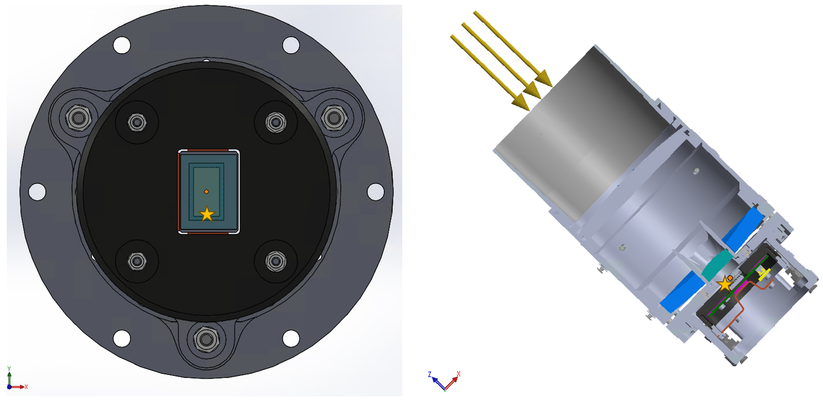
The optical instrument (OI) analysed in this work is a major element of the cubesat mission designed for hyperspectral imaging. It is supposed to operate in low Earth orbit at an altitude of 500 km. The instrument has a field of view of 2.5° and a focal length of 135 mm. Its total weight is 2.7 kg, and its approximate dimensions are 2U (200 × 100 × 100 mm). The positioning of the OI in the entire satellite can be seen in
Figure 1.
A CAD model of the optical instrument was used for all analyses in this paper. It is shown in
Figure 2 next to a photograph of the assembled instrument. The difference (absence of the red mounting part and the board at the back) is only due to the preparation of the experiments; these elements were used in the final assembly of the Intuition-1. The OI consists of a body, a set of lenses, and the most important component for image capture, the CMOS (Complementary Metal Oxide Semiconductor) image sensor. CMOS imaging technology is designed to convert incoming light into digital images. The sensor detects incoming light using thousands of photon detectors on the surface of a semiconductor chip. The purpose of each detector is to measure the frequency (colour) and number (brightness) of photons absorbed and convert the photon energy into an electrical current. This current is then amplified by transistors connected to each detector. Because the CMOS image sensor is exposed to incoming radiation (directly from the Sun or reflected from the Earth) and has to process a huge amount of signals, it is at risk of overheating and damage. For this reason, its thermal state should be analysed at different stages of operation. It should be noted that damage to the CMOS image sensor would render the entire satellite unusable.
In order to monitor the temperature of the image sensor, a dedicated temperature sensor is integrated within the CMOS device, as indicated by the star symbol in
Figure 3. It is essential that the temperature measurement be as precise as possible in relation to the CMOS while ensuring that the imaging capabilities remain uncompromised. The temperature sensor is integrated into the CMOS structure, and its position is fixed. It was of great consequence to the findings of the experiments, which demonstrated that the temperature measurement does not accurately reflect the highest temperature, which could prove fatal for the image sensor.
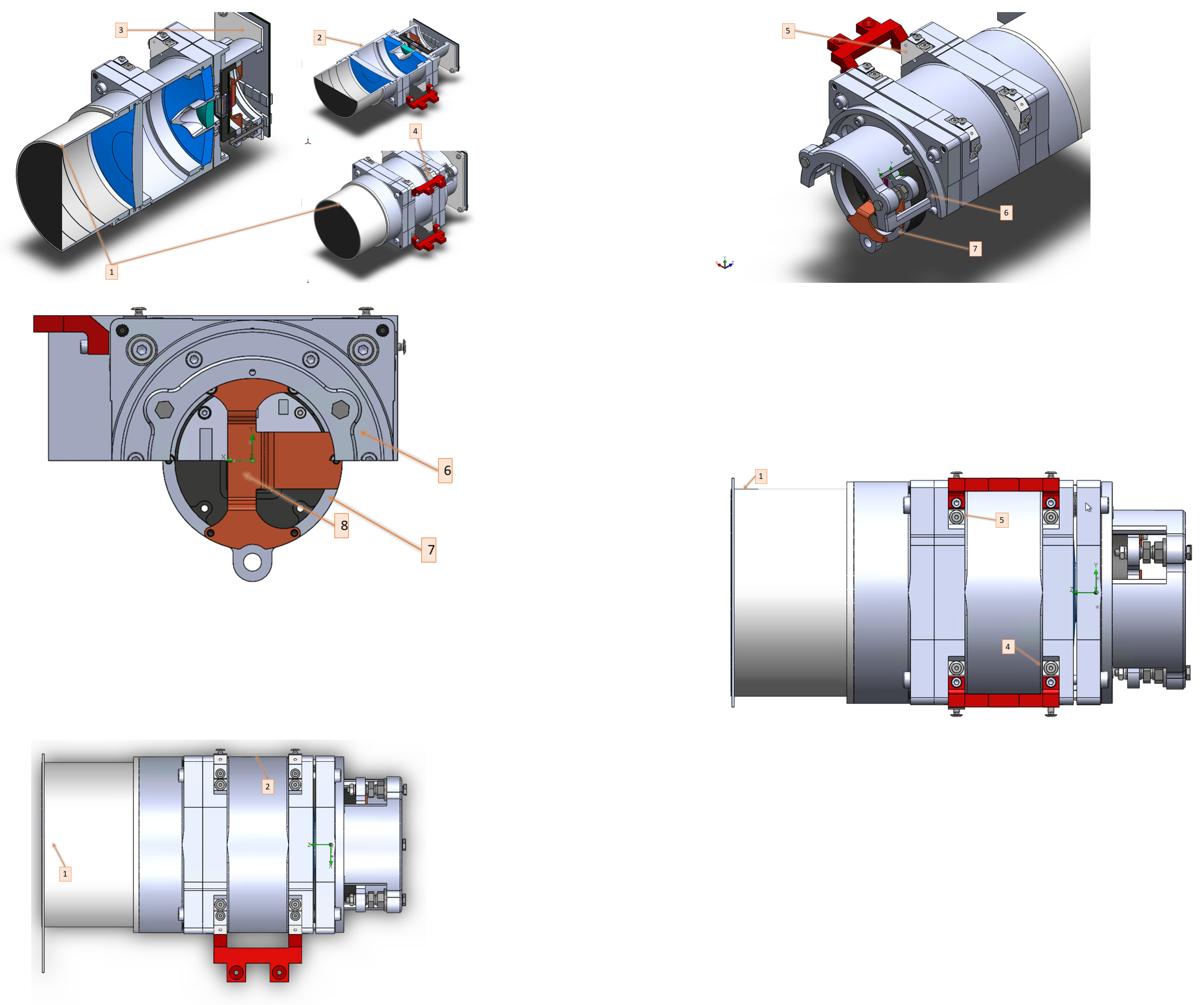
In order to conduct in-orbit experiments, additional sensors were installed in accordance with the configuration depicted in
Figure 4. This configuration also corresponded to the probe positions utilised in the finite element method (FEM) analysis. The sensors are designed to monitor the most significant heat paths during the normal operation of the satellite. The temperature of the OI structure (sensors 1, 2, 3, and 6), the temperature at the juncture between the OI and the I-1 (sensors 4 and 5), and the temperature of the copper connector between the CMOS and the structure (sensors 7 and 8) were monitored.
The OI elements in contact with the lenses are built from alloys with a low coefficient of thermal expansion. Moreover, similar values of the coefficient of thermal expansion for glass and the alloy used in this case allowed the minimisation of mechanical stresses and potential distortion within the temperatures expected in the structure. Since the structure had to dissipate some of the heat from incoming light (direct sunlight or reflected by Earth), thermal conductivity was also of interest, although secondary. From that perspective, the material choice surrounding the CMOS array and the printed circuit boards (PCBs) was much more important. The design had to dissipate heat efficiently, and only mounting pressure was used to limit the thermal resistance of the contact pair. Solid pads were chosen as thermal interface materials with mixed selection depending on whether or not electrical conductivity was desired in a given area. Finally, the conductivity through the mounting bolts was interesting because it provided a thermal bridge between the active electrical components (the sources of most of the heat in the OI) and the cubesat structure (which was connected to cubesat heat sinks of relatively constant temperature).
3. Operation Scenarios
The principal function of the satellite in question is to obtain images of the Earth. This involves the sequential activation of the imaging system and the processing of the received light signals. However, while the satellite is in operation, unforeseen circumstances can arise that result in the CMOS chip, which is susceptible to temperature fluctuations, being subjected to uncontrolled temperature increases. This could ultimately lead to chip failure. Such circumstances could include the satellite being inadvertently pointed towards the Sun or the optical system being accidentally directed towards the Sun. Therefore, three operational scenarios were considered for the numerical simulations.
The scenarios analysed in order of complexity:
3.1. Sun Pointing
In this scenario, the optical instrument observes the Sun from Earth, while an external board is used for data acquisition and virtual mission control. This case serves as a correlation to the simulation. It is similar to the more dangerous scenario, in which the OI looks directly at the Sun while in orbit. It is highly unlikely, but it represents the worst-case scenario. For experimental validation, the OI was placed in an angle-activated mount in a shaded area with a retractable roof, as shown in
Figure 5. This allowed the OI to be pointed directly at the Sun and then exposed to control its heating from ambient to a temperature unsafe for the instrument.
3.2. Inadvertent Sun Passing
During the de-tumbling process (in orbit), when the satellite’s movement is still not fully controlled (due to the speed limitations), the optical instrument looks in the Sun’s direction while moving as slowly as possible. A hotspot (point of focused sun rays) moving through the diagonal of the CMOS array represents our worst-case scenario, in which the CMOS array heats up. The hotspot size is the result of the sun-ray path through the lenses and mirrors system, and with random and relatively fast rotation, the average temperature of the optical instrument structure is considered stable and averages 0 °C. The hotspot moves from one corner of the CMOS towards the opposite corner in 27 s. This movement occurs due to the minimum rotational speed, set at 0.2 deg/s, which allows traversal of the diagonal of the CMOS array. This rotational speed results in the hotspot’s linear motion at 1 mm/s.
A time-dependent simulation was performed to model the 0.5 s process, and its results were imposed as the initial condition for a subsequent 0.5 s simulation with the focal length shifted by 0.5 mm. This was performed because a full simulation of light passing through a lens with sufficiently high resolution to capture a sharp focal point is computationally too expensive. Furthermore, in such a short time, most heat does not have enough time to pass through the structure surrounding the CMOS. There is not enough time for the baffle to heat up as well.
It is important to note that the entire test was conducted manually. The covering and uncovering of the apparatus was performed by a laboratory technician, and the orientation of the OI towards the Sun was facilitated by a gnomon setup. While the data were acquired by the same system that would be used in satellite operations, the system was connected externally. These limitations (angular positioning with the naked eye and uncovering with the limits of human reflexes) may potentially influence the results to a slight degree. A difference of a few degrees in pointing towards the Sun or even a whole second of delay would be discernible in the results (a shift to the right or a less pronounced slope of temperature gain). In the tests performed and used in this study, such problems were not observed. However, they are common with similar test cases of other equipment tested by the team.
3.3. Earth Imaging
In this scenario, the optical instrument takes images of the Earth. From the thermal perspective, each imaging starts from positioning the OI, which means it is directed towards the Earth. Then the CMOS is turned on and starts dissipating heat. Subsequently, scene acquisition starts, with even higher heat dissipation, and lasts 20 s. The electronics are turned idle for 2 s and then off for 10 s. Next, another imaging is performed (electronics turn to idle and then scene acquisition). Imaging of the Earth takes place in orbit, so the temperature of the outer walls (from the perspective of the optical instrument, these are not necessarily the outer walls of the entire spacecraft) in these conditions will remain mostly constant, as seen in
Figure 6. This is based on ESATAN calculations performed by the KP Labs team; details of those calculations are not parts of this study. The imaging can be easily controlled, and depending on circumstances, imaging frequency might be as low as one per orbit. However, to analyse thermal performance, some of the possible operating cases are described below.
The thermal boundary conditions set for this study were the following:
The radiation source (to element 1 in
Figure 4);
Heat sources (elements 2, 3, and 4);
Constant temperatures on the external structure.
The in-orbit activities are explained further in the following tables. First, the most basic scenario is shown in
Table 1 with two acquisition scenes. The beginning is the steady-state conditions with the electronics turned off, and the entire analysis ends after 56 s of physical time.
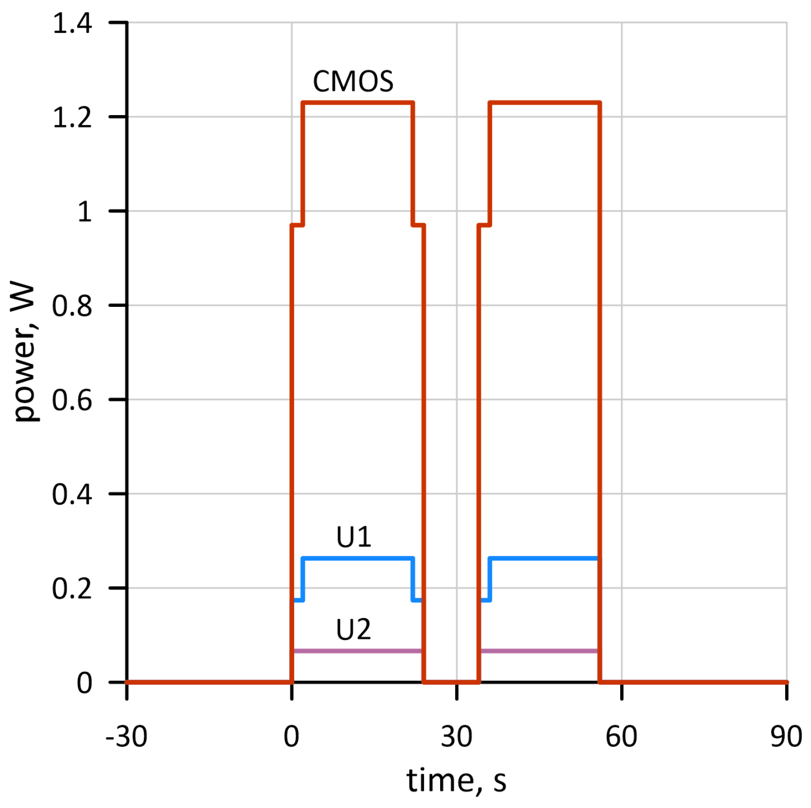
The elements presented in this paper are those three with the highest heat dissipation. They are referred to as CMOS, U1, and U2, and they had a much larger contribution to the total power compared with the rest of the components. The power dissipation of the other components is considered negligible.
Finally, advanced scenarios were considered. They consist of scene acquisitions repeated after a certain time. In the case considered for this work, that time was 90 s. The dissipation of heat throughout the scenario is seen in
Table 2 and is presented graphically in
Figure 7. Initially, it was assumed that the instrument would fully cool down during a 90 s pause, and this hypothesis was tested during “Earth imaging” analysis, described in detail in further sections.
4. Numerical Model
The model consists of the outer structural elements of the cubesat, an optical system, CMOS, PCBs, and connecting parts. The geometric simplification started by excluding details that did not impact heat transfer (pins protruding from surfaces, cables below 0.25 mm diameter, and screw recesses). The threaded connections were then simplified to cylindrical surfaces. The contact conductance according to the Yovanovich formula is very high, based on the relatively large contact area of the threads, the pressure between the materials, and the low surface roughness. Furthermore, when considering metric threads, the contact area is 5/8 of the thread height H swept along the helical profile, and when substituted by a cylinder, it is half the pitch area (i.e., ) swept along the same profile. Surfaces differ only by 8% while a perfect contact on the thread is considered. Moreover, in the case of real contact, the difference will be even smaller.
Thermal pads were considered as solids with thermal conductivity as a function of applied pressure, according to their manufacturers’ data sheets. Extremely simple correlations were performed for the copper plate–thermal pad–copper plate assemblies, and it was found that manufacturers overestimate their thermal conductance value. These experiments will be further investigated in future work, while the measured value was used for this study.
The following sensitivity analysis performed in the more advanced screw assemblies [
29] was simplified to 1D connections. Thin sandwich structures (thermal pad stacks where thermal conductivity and electrical insulation were necessary) were simplified into substitute blocks with material of average thermal properties (in this work no electrical simulations were performed). Thermal gels and pads were treated to perfectly fill in the gaps. Sensors (1×1.5×2 mm) were excluded from the simulations as they have an extremely low heat capacity but would require dense meshing. Non-dissipating small electronic elements were also excluded if they were in contact only with the PCB and were not used as thermal paths. Eventually, where possible, the structure was simplified and equivalent resistance was used. The same numerical model was applied in each case. The only change was the boundary conditions collected in
Table 3.
For the cases considered, the external heat sources were assigned constant values. In other words, differences in Earth’s albedo over different regions were not considered. Earth’s heat flux was deemed equal to 364 W/m2 (based on Stefan–Boltzmann). It is extremely important to note that for the Earth imaging scenario, the effective area of the satellite is only its optical instrument entrance – the rest of the surfaces were treated in Esatan-TMS, and heat radiated from Earth is applied in boundary conditions of outside walls. For the inadvertent Sun passing, the Sun was considered the source with 1360 W/m2 unobstructed by absorptance of the Earth’s atmosphere. For the Sun pointing, direct solar irradiance was calculated for the day of the experiment (visually clear sky, close to zenith, short time of experiment).
In the case of the Sun-pointing scenario, due to software requirements, the simulation had to be divided into two parts: heating and cooling. It was nearly impossible to turn off the global solar radiation boundary condition. The workaround used was to turn on the sunlight for the heating phase and then transfer the results to a cooling simulation with the sunlight turned off. The grid settings were consistent with other analyses in this paper. Based on the calculated Rayleigh criterion (Rayleigh number of 670), heat transfer within the OI is by conduction in the air rather than convection. Therefore, flow turbulence and natural convection inside the OI were not part of this study. The heat source was set up as follows: direct irradiance was calculated from total solar irradiance, taking into account the weather conditions (clear sky with no visible clouds and humidity) and the relative position of the Sun at the time of the test. After calculating the surface power density entering through the front lens, it was used as a parallel radiation source with wavelengths corresponding to solar radiation after scattering in the atmosphere. A comparison of analytical results and correlation with experiments was also carried out to prove the accuracy of the model.
The simulation software had one important limitation. All objects had to have thickness and material properties, including the source of the incident light (even though they were abstract). Because of this requirement, the radiating surface had one side facing the CMOS, called the “light surface”, and the other side facing away from it, called the “shadow surface”. The temperature of the “shadow surface” was equal to the Earth’s average reference temperature of 15 °C. In contrast, the ‘bright surface’ was the source of radiation for the Monte Carlo simulation, with a distribution and wavelength corresponding to the Earth’s spectrum. To avoid conductive heating from the edge of this object, an extremely high (virtually infinite) resistance was set there. The rest of the thermal contact resistances were set according to simple assembly correlation formulas or conformed to the investigations of the thermal conductivity between metals by Yovanovich [
15].
4.1. Monte Carlo Approach
The Monte Carlo method for radiative heat transfer is a statistical technique that simulates radiation by randomly tracing paths of energy bundles, or rays, through a system with complex geometries or participating media. The process commences with defining the system geometry, surfaces, and properties, including emissivity, reflectivity, and transmissivity. The emission of rays is performed randomly from points on radiating surfaces, with directions chosen according to the cosine distribution if the surfaces are diffuse. Each ray represents a proportion of the total radiative energy, and its trajectory is traced as it traverses the three-dimensional space. The probability of a ray being absorbed, reflected, or transmitted when it encounters a surface is determined by the surface’s probabilistic properties. In the case of participating media, such as gases or semi-transparent materials, the absorption or scattering of rays within the medium is also determined at random, based on the material properties of the medium in question. This has the effect of influencing the distance that a ray travels before being absorbed or redirected. The aforementioned process is repeated with a substantial number of rays to accurately model the radiative heat flux. This is achieved by summing the contributions of absorbed, reflected, or transmitted energy at each surface or region. The Monte Carlo method is widely used due to its adaptability to complex systems. However, it is important to note that it can be computationally expensive. Nevertheless, it lends itself well to parallel processing, allowing for efficient simulation.
Monte Carlo modelling of radiation was used in all calculations carried out using the FloEFD 2205 software. The total number of rays was initially set to 3 million, with an additional 3 million rays generated from the light source. This number was increased incrementally as required.
The rays were initiated at a surface that actively dissipated heat and at the entrance to the optical instrument. The initial analysis was conducted with one million rays, which proved to be a stable approach, although the resulting resolution was not optimal. To assess the impact of increasing the number of rays, the analysis was repeated with 2 million rays. This led to a slight increase in the overall runtime, indicating that the computational cost associated with the Monte Carlo method was not the dominant factor in the overall analysis. To further enhance the precision and reliability of the results, a final increase to 3 million rays was implemented.
4.2. Mesh
Generating the mesh was a step-by-step process. The first step was to generate the mesh with uniform 2.5 mm hexahedral elements. This was sufficient for most of the structural components that did not generate heat and were not in the vicinity of such bodies. Secondly, a mesh was generated for the PCB, which consisted of 0.005 mm hexahedral elements. The third step was to refine the part mesh with expected high temperature gradients, low-quality mesh elements, and bodies with overly coarse meshes. All of these operations resulted in about 7.7 million cells, where the regions with the highest mesh density were the PCBs, CMOS, light source, and thermal interface materials. It is important to note that in order to replicate this analysis, the PCBs were created using a “smart PCB” model using the EDA Import tool, a specialised add-on used in the FloEFD software to import electronic components and PCBs. It allows for importing rather than reapplying material properties and component relations. Especially junction-to-board and junction-to-case conductivity are crucial for assuring adequate thermal contact relations.
Figure 8 shows the mesh in cross-section through OI and a view of CMOS.
A particularly dense mesh was generated for components suspected to be in the main heat flow path. These areas were refined based on preliminary results to improve grid quality in regions with high temperature gradients. Of the total of 2.62 W of energy from Earth’s radiation, 2.344 W hits the CMOS chip and its surroundings directly.
The Monte Carlo method for radiation analysis was used with 3M rays starting at the virtual surface, representing rays incoming to the OI. The time step was chosen on the basis of a sensitivity analysis for all cases, ranging from 0.5 to 1 s, as this resolution was sufficient. A similar baseline mesh was used in all cases, with additional refinements focused on lenses, PCBs, CMOS, and contact areas. the difference between the three analysed load cases was in the external elements, i.e., the cubesat structure for Earth imaging and inadvertent Sun passing, and positioning elements in the case of Sun Pointing.
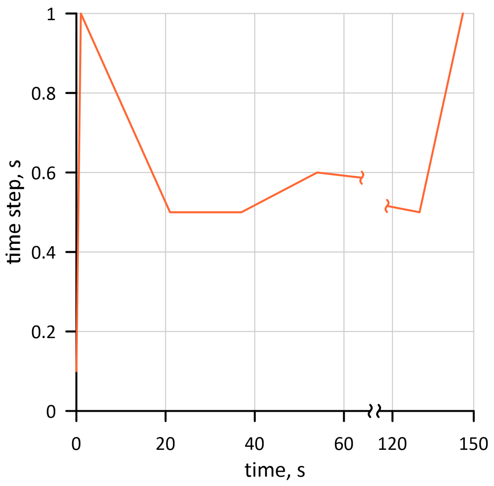
4.3. Time Step Optimisation for Earth Imaging Scenario
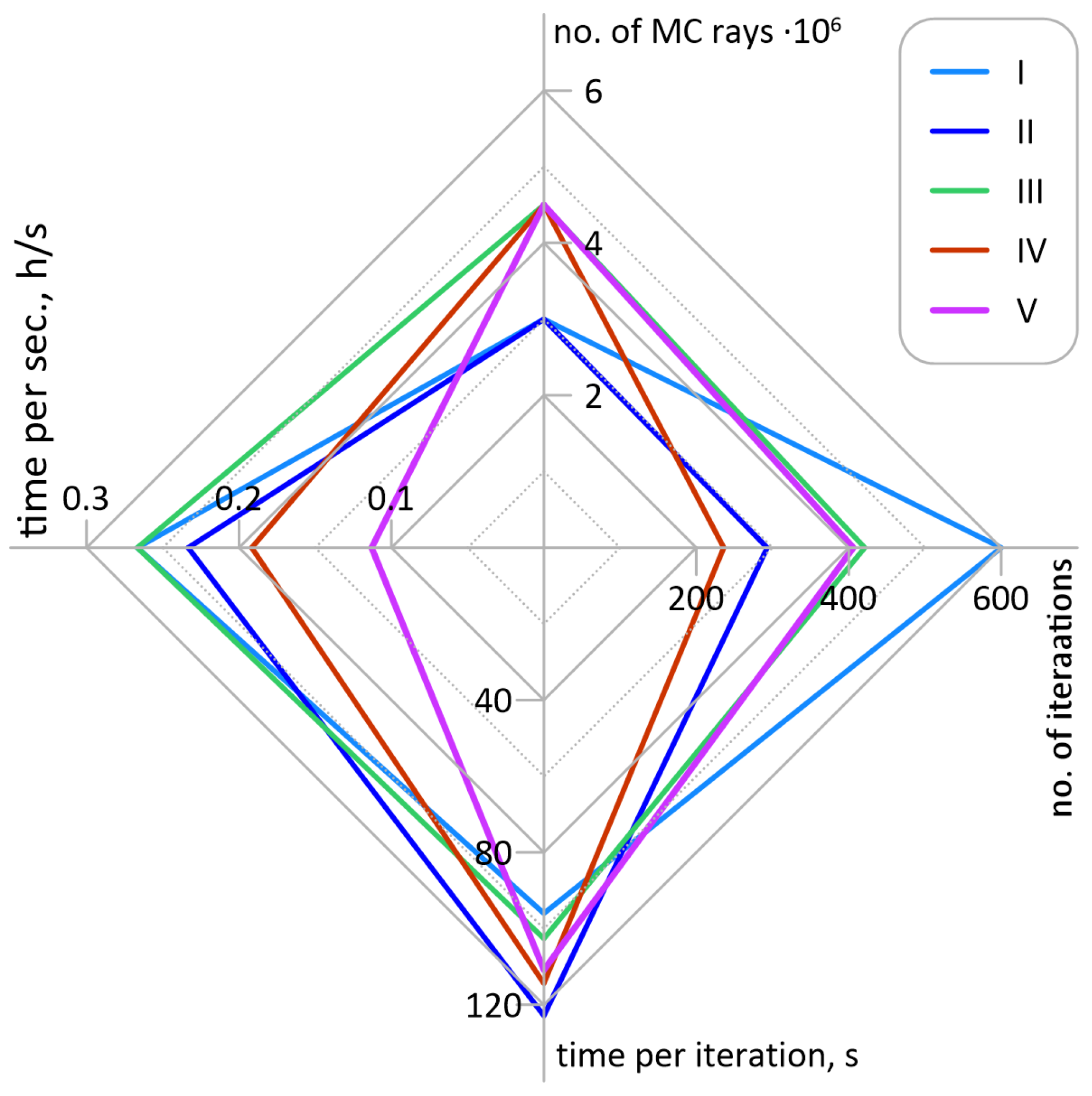
For each analysis, the time steps were optimised in terms of analysis time. This was important because the optical instrument was under development, and changes had to be introduced evolutionarily and their impact checked. The optimisation process had a simple aim—to ensure that the analysis was error-free and stable while being as short as possible. As different times were calculated at different stages of model development, some metrics were introduced for comparison, as shown in
Figure 9. The first was the number of MC rays—more was considered better, allowing for better resolution of the results. The second was the computation time required per second of simulated processes; the lower, the better, as it saves time. The number of iterations was a native metric of the software, and again a lower number was advantageous, similar to the time per single iteration. The time per second (left arm of the graph in
Figure 9) was the leading parameter in the optimisation.
The time–step ratio is calculated as the total number of time steps divided by the physical time. Starting from an average time–step ratio of 10, the time step was increased. The increase was not uniform and focused on the main points: initialisation, inclusion of additional heat sources, and cooling. Details of the time–step strategies are shown in
Figure 9. The optimisation algorithm was based on a simple greedy algorithm – the time step was increased until failure. Failure was defined as nonphysical results (e.g., temperature rise in the absence of heat sources). After the optimisation, a small override was made for the calculation number V, since it was observed that during cooling in repeated cycles (above 3), the solver is less stable and requires a denser time step than in single imaging (two scenes acquisition as seen in I to IV).
The optimisation algorithm used can be seen in
Figure 10. Before starting the algorithm, the number of time steps was increased around the activation of heat sources. If the simulation was unstable, a local reduction in the time step was introduced, which means the time step was adjusted to simulation demands in the problematic period. Alternatively, if the simulation was stable and accurate, the time step was increased globally to save computational time.
Additionally, a high time–tep density was established for the initial phase of each simulation to allow for a smooth transition. Surprisingly, these were not the critical moments for the stability of the solver. The initial strategy was flawed and overlooked a major problem. The stability of the solver turned out to be quite resistant to long time steps for most of the computation periods. In particular, when multiple heat sources were involved, the simulation was stable even for impractical time steps (due to reporting problems) longer than 1 s. However, there were stability problems during the cooling phase of each cycle (the unstable solutions are not shown in the graphs presented in this work). Most of the errors occurred in the middle of the period when all electronics were off. Due to that, the idea of “increased sensitivity to reduced constraints” appeared. As a test, a drastic increase in the time step for the working phase (electronics idle or on) was carried out and showed no effect on the stability of the calculations. Next, a similar increase was introduced to the cooling phase (all electronics off), and the solutions were unstable (or a non-physical behaviour occurred). Finally, an even more relaxed approach to the working phase and a rigorous one to the cooling phase resulted in more efficient calculation times and calculation time per physical time.
It was observed that the solver was significantly less stable and more prone to numerical errors during the cooling phase (all heat sources were off). The software had a tendency to create nonphysical heat sources that operated in a single iteration. This proved to be the main instability of the calculations and the strongest limitation to further time–step reduction. The overall time step was increased, resulting in the ratio dropping from 10 to 0.36 and finally reaching 0.99. It could be further optimised in some physical time ranges (namely the heating phase), but the gain in computational time would be marginal: the improvement from 1.1 to 0.99 resulted in a reduction of less than 0.1% of the computational time. The optimal time–step strategy is shown in
Figure 11. It is worth noting that the time steps are shown exactly and changed from one set time to another. For example, the first iteration for this strategy started at 0.05 and grew linearly towards 1 in the second one. This means that there were four iterations, each with a larger time step. Then it changed as shown in
Figure 9.
Initially, the simulations (simulation I in
Figure 9) were run with automatic initialisation to introduce initial temperatures (global 15 degrees, walls 0 degrees, as shown in
Figure 6). This resulted in a high initial computation time, which had to be repeated for each run. The steady-state initialisation was used to save time by allowing the steady-state solution (4 h) to be reused as the initial condition without the need for recalculation. The temperature distribution was physical rather than artificially hard-bound. The steady-state initialisation is the basis for all optimised runs, drastically reducing the number of initial iterations required.
In general, the optimisation was an iterative process explained in
Figure 10. Initialisation was considered a special case of locally reducing the time step due to stability problems.
The computing time, as one of the most valuable pieces of information, is considered in the graph in
Figure 9. Along with it are the number of iterations (a right arm of the radar plot), the number of rays used in the Monte Carlo method (upper arm), and the computational time per second (hours needed for one second). The time required to compute 1 s of physical time was compared between different setups in time. Shorter time steps were required at the beginning of the computation, suggesting that a pre-initialised computation might be advantageous. Manual initialisation by steady-state computation took about 4 h, and this time was added to the total computation times. However, in the optimised simulations, it was performed only once and reused, reducing the total time.
For in-orbit scenarios, convective heat transfer was not considered. However, in additional tests used to determine correlation parameters, convection played a significant role in defining the thermal resistance of the pins, although slightly less so in the Sun-pointing tests.
5. Simulation Results
The operation scenarios described in the previous section were numerically simulated to determine the maximum temperature within the elements and the danger of their thermal deterioration.
5.1. Sun Pointing
The simulation was performed with the same mesh settings as in the general settings in
Section 4.2. Since this scenario affects the operation on Earth, air at a set ambient temperature was introduced into the model. Heat conduction through the air in narrow spaces was included in the calculations, based on Rayleigh number criteria. The time of 26 s of the experiment was too short to noticeably change the temperature of the outer wall, which was consequently assumed to be equal to the ambient temperature. Free convection from the baffle walls (outer) was also not modelled, simplifying the calculations and saving solution time. Due to the very low Rayleigh number (small gaps), the heat transfer through natural convection in trapped air in the OI was not important. This assumption has a marginal effect on the results, and its impact is not measurable in the experiment. The sensor’s temperature in the simulation is shown in
Figure 12.
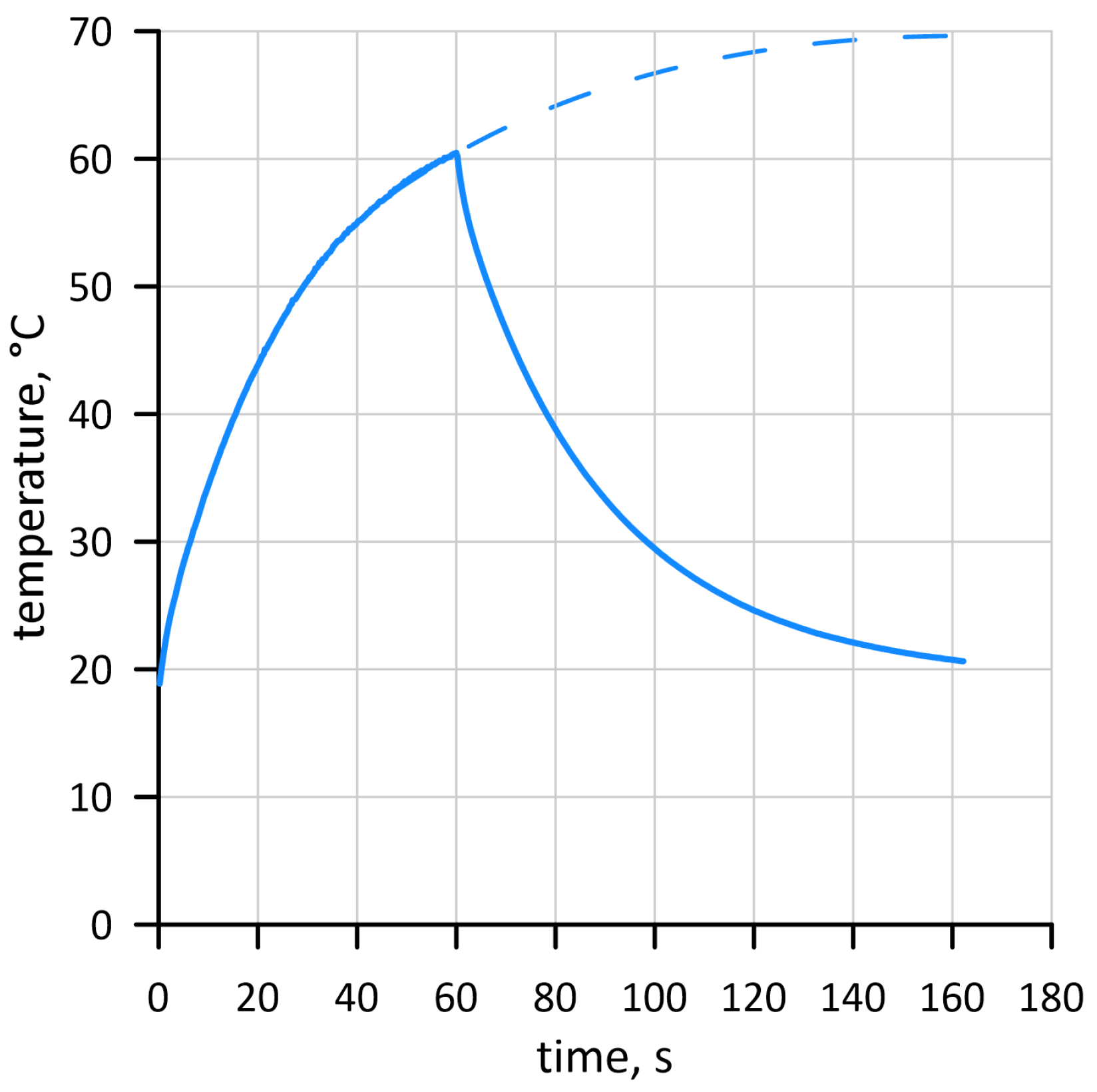
The results shown in
Figure 12 demonstrate the heating of the CMOS array, where the observed rapid temperature rise immediately after exposure to the Sun quickly reaches a dangerous 60 °C. As can be seen, the slope of the curve decreases with time. In extrapolating the curve, a constant temperature of about 70 °C is expected. Unfortunately, such an experiment would be too dangerous for the CMOS array and could not be performed.
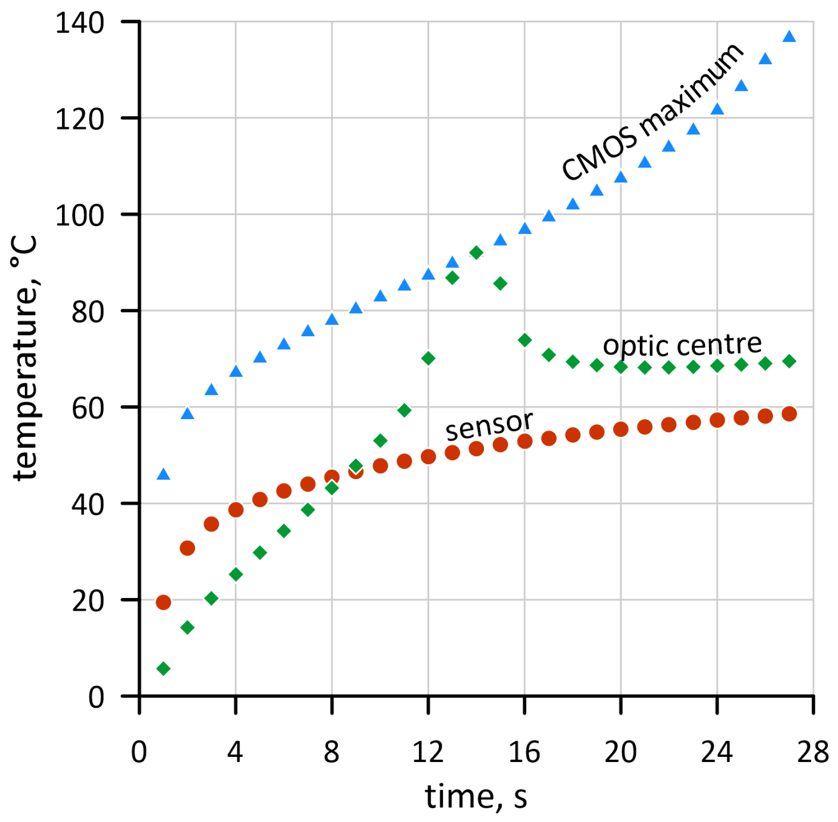
5.2. Inadvertent Sun Passing
In the simulation of the second scenario, three important points were analysed: the optical center of the CMOS, the temperature sensor (located at the edge of the array), and the hot spot (point of highest temperature). The main purpose of this distinction was to understand which case was the worst and what the actual temperature difference was between the sensor reading and the maximum temperature. Four different hotspot paths are along the CMOS diagonal, starting at any corner and moving towards the opposite corner. As the greatest difference would be obtained if the hotspot started close to the sensor, it was chosen for the simulation. It can be seen in
Figure 13 that the difference might be as large as 80 K and that the sensor does not report the actual maximum temperature in all cases.
The difference between the observed points can be seen in
Figure 14. Since the difference between sensor reading (temperature of a point placed on the edge of CMOS) and hot spot can reach even 80 °C, relying on it to maintain safety is dangerous. Despite the high conductivity of the material and due to the short time of high-energy flux, the sensor would not accurately report that the dangerous temperature of 85 °C was exceeded. This analysis ignores the fact that the sensor has a limited response time, which can further impair its ability to report the actual temperature. Due to the hardware limitations, the reference point temperature considered safe was therefore set at only 60 °C.
5.3. Earth Imaging
FloEFD software, preferred for the thermal analysis in this case, had to be tested to determine whether it appropriately captured the optical properties of the instrument. To ensure that a comparison was made between the FloEFD and Zemax simulations, software dedicated to such calculations was used. The results can be seen in
Figure 15. In
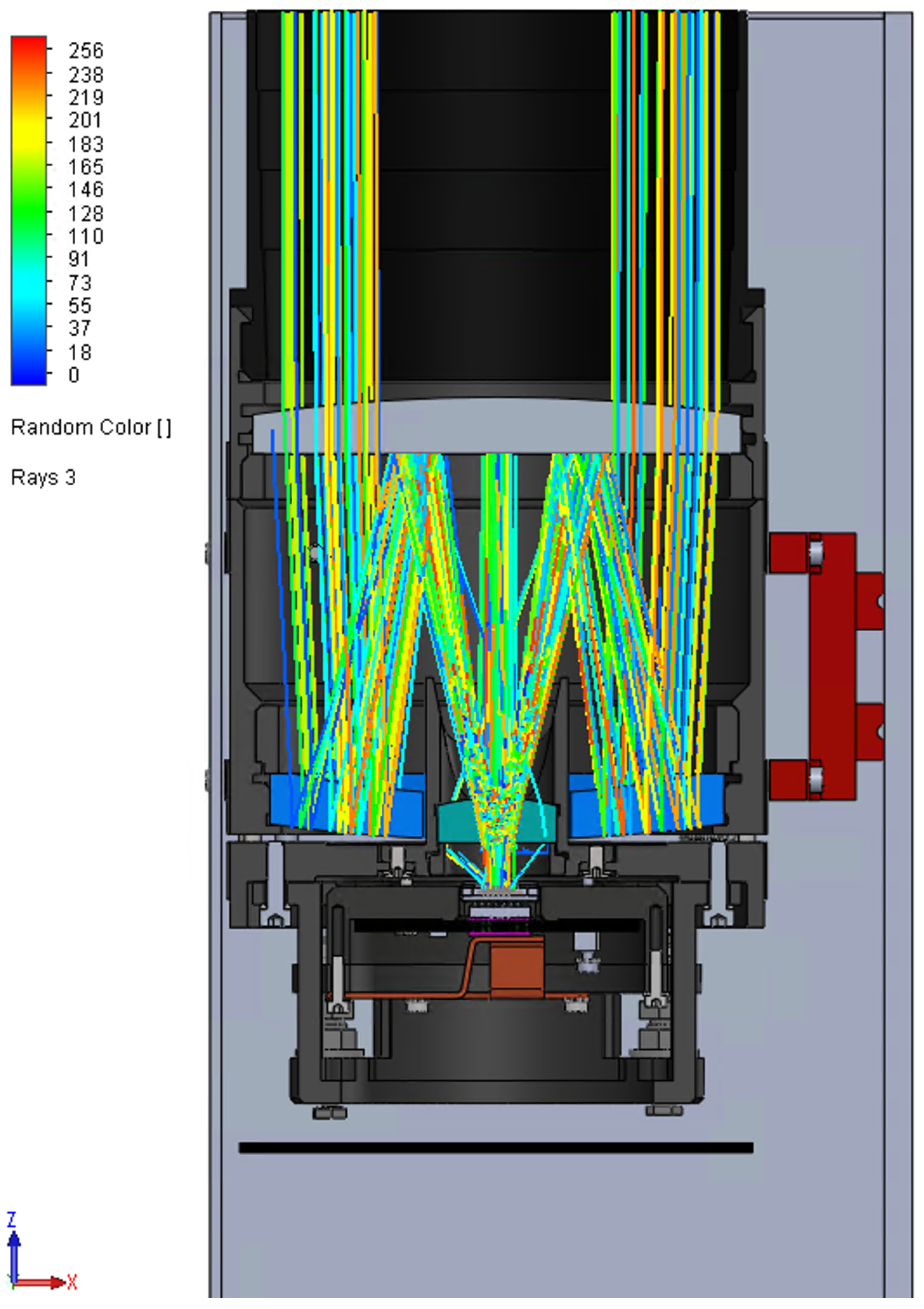
Figure 16 the ray path in the whole OI can be seen.
Zemax allows for capturing substantially more information (and with higher accuracy) about rays’ behaviour. However, FloeEFD offers CAD integration and extensive thermal modelling. Since thermal modelling was the main part of this work and, at the time of those calculations, Zemax did not offer native integration, the FloEFD was chosen as the main simulation software. Assuming that FLoEFD is supposed to focus solely on the thermal aspect of the incoming rays, it was considered satisfactory to neglect spectral scattering for those calculations. The rays in the whole OI interact mostly with lenses and the CMOS array, not increasing the temperature of the walls in the steady state.
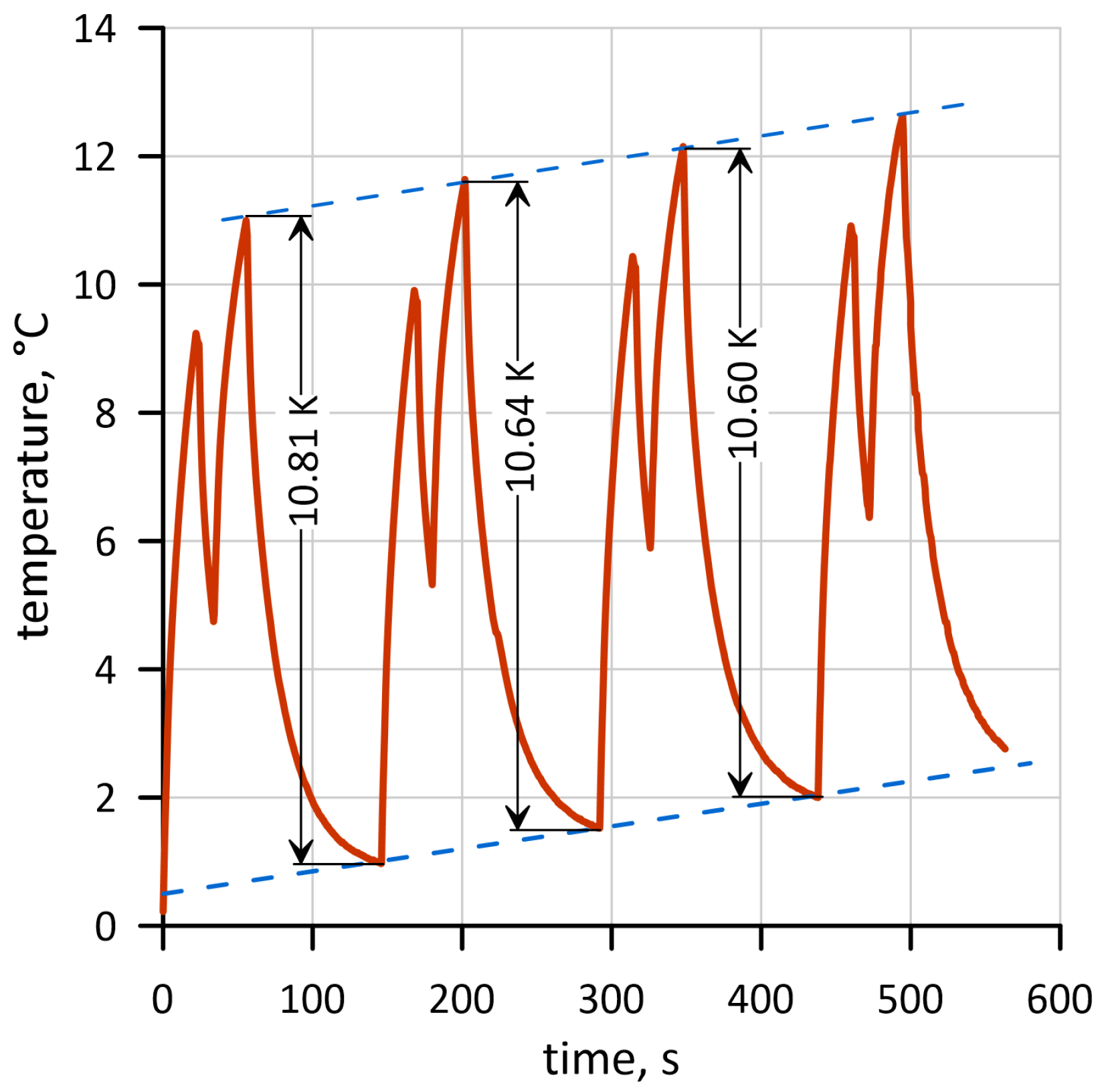
The peak temperatures between cycles grow linearly for four consecutive cycles of imaging reported in
Table 1 +90 s pause. A single cycle between 0 and 146 s is shown in
Figure 17 for one data series. After the first imaging cycle, the peak temperature is slightly above 11 °C and is far from a dangerous zone. The purpose of the study was to analyse the cyclic behaviour so that the next cycle starts where the former ended. The end temperature of cycle no. 1 is the initial temperature for cycle no. 2, and so on. The temperatures from the cycles’ starts and peaks were used for linear extrapolation of the difference between them, and for all the modelled cycles, it was almost constant, ranging from 10.81 K to 10.60 K. Similar linear behaviour is observed for the final temperature in each cycle. The slow decrease in temperature difference can be attributed to a higher difference between the hot CMOS surroundings and the cold boundaries kept at 0 °C. This difference increases the heat exchange rate. The effect is minuscule and within the solid safety limit. The temperature creep between cycles can be assumed to be less than 1 K. This means that by imaging alone, the CMOS will never reach a dangerous temperature level. The dangerous temperature for the CMOS was not reached in the simulation, as it would require simulating hours of physical time. Potentially it could be achieved with a much higher initial temperature, above 50 °C, or in the case of different boundary conditions (for example, a higher temperature of the external walls). Shorter intervals and more imaging cycles are potentially possible if necessary, but additional investigation is needed.
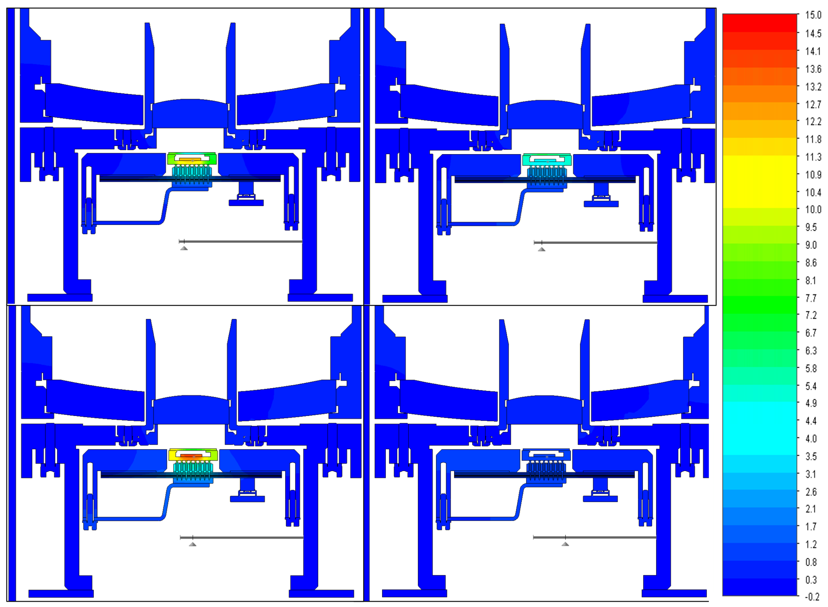
The change in temperature in the OI is limited to the surroundings of the heat-dissipating elements and the CMOS that are heated up by the incoming rays. The visualisation of temperature changes in the CMOS vicinity is shown in
Figure 18.
The temperature difference from the start to the peak is estimated to remain within a range of 10–12 K.
The final temperature of each cycle is around 0.7 K higher than the final temperature of the previous cycle. The increase between cycles is almost constant, as can be seen in
Figure 17. A similar increase is observed for the highest temperatures. A slight shift, less than 1 s, is observed for the peak temperature occurrence time.
6. Experimental Validation
The Sun-pointing experiment was designed to determine how quickly the CMOS temperature rises when the Sun is in its field of view. Looking directly at the Sun poses a significant risk of overheating and represents an orbital situation where the OI is in an unfavourable position due to a positioning error. The experimental setup consisted of the optical instrument, data acquisition setup, connectors, holder, and blinder (to shield the OI from sunlight between experimental sets). The main difficulty was the practical nature of this experiment, which meant that a clear sky with low humidity and the Sun close to the zenith was preferred for correct hazard assessment. The instrument had to be positioned without exposing the CMOS to sunlight (so the optical system could not be used to position itself). A simple gnomon was used to position the covered OI, and then the setup was secured in a holder. There was a limited time to start the experiment from this point, as the Sun was out of view of the OI within minutes.
Each measurement consisted of the following steps: uncovering the OI, observing the Sun until the CMOS-embedded sensor showed 60 ° C (temperature deemed dangerous), covering the OI, and measuring the cool-down time.
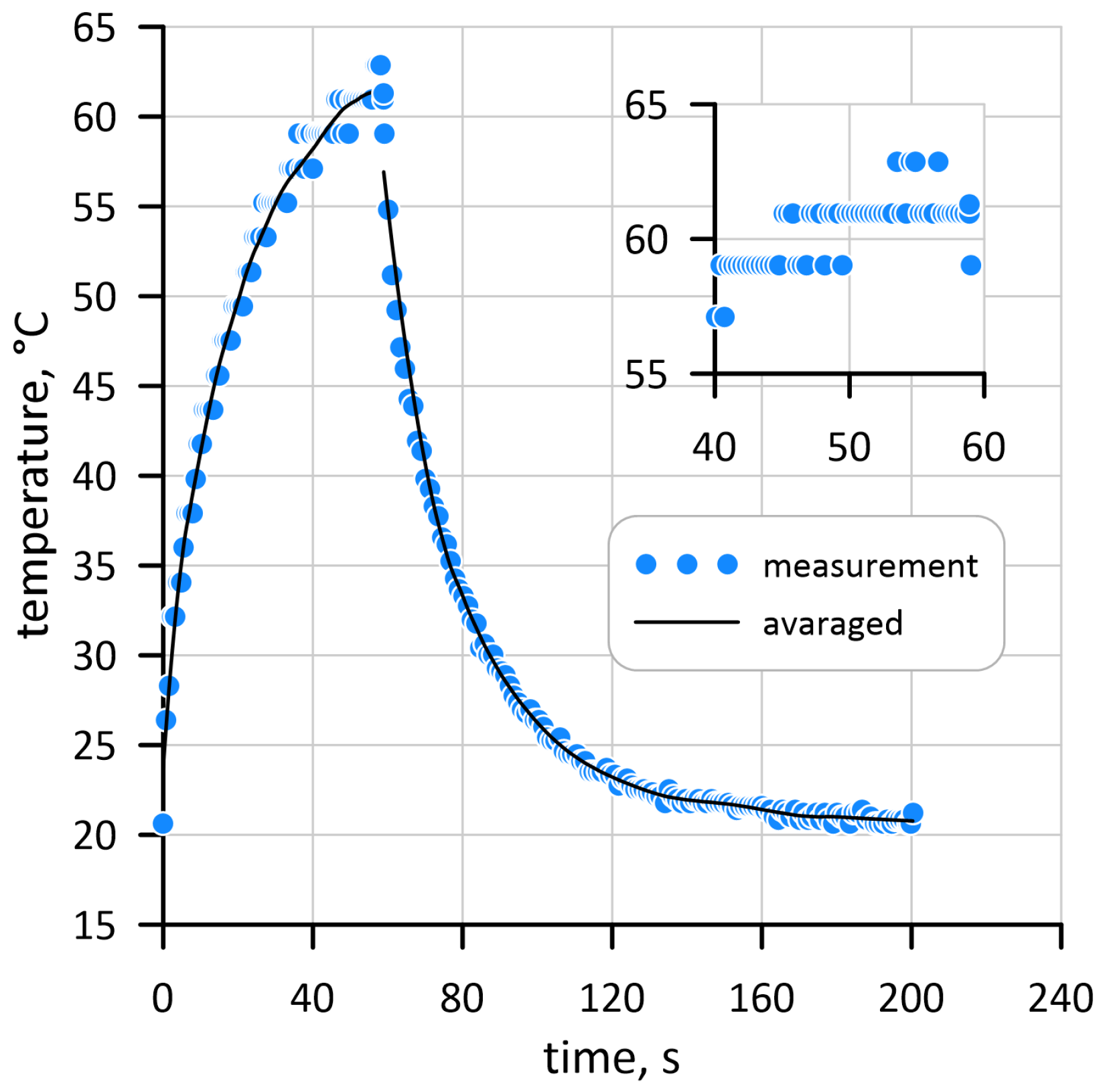
The acquired data was in the form of discrete readings from the sensors built into the CMOS. It has a limited resolution, so the readings close to the threshold were slightly unstable, as shown in the enlarged section in
Figure 19. The changing readings over a second made it difficult to read out the measurements and control the temperature in real time.
To make the results easier to view and compare, they have been averaged over time and plotted at intervals of 1 s. Unfortunately, this increases the noise in the data, and the graph is noticeably less smooth than expected for point-source heating and cooling. However, the averaging enhances data perception and allows for its juxtaposition to the numerical results. The averaged temperatures from the experiment can be seen in
Figure 19.
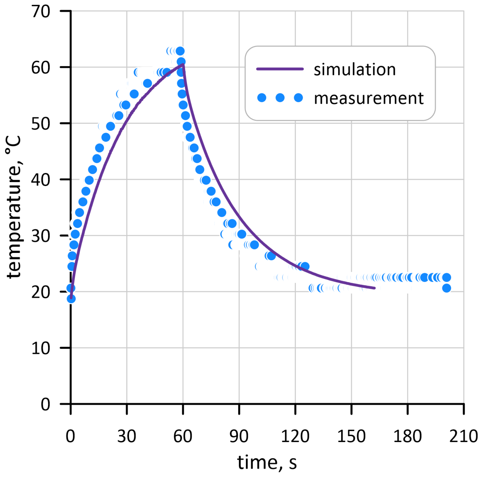
A comparison between the experimental results and the numerical simulation can be seen in
Figure 20. The heating phase of the experiment is largely in agreement with the numerical analysis, and the error is well below the resolution of the sensor. A larger discrepancy can be observed during the cooling phase. In the experimental study, it was faster, reaching the room temperature after only 60 s (around the 150 s label). In the numerical study, the cooling took up to 160 s to reach the same stabilised temperature. Given the more pronounced arcs in both cooling and heating, it is plausible that the thermal conductivity of the CMOS pins and surroundings is higher than expected. Alternatively, or coincidentally, this could be the effect of the hot spot shifting relative to the sensor location during the experiment. Overall, the differences were small enough, especially during the heating phase, that the reliability of the computational model can be accepted.
In light of the aforementioned remarks regarding measurement quality, a number of potential improvements emerge. From a theoretical standpoint, the optimal approach would be to increase the number of sensors in order to account for the delay caused by heat transfer from the hot spot to the sensor. Maintaining a single sensor would be advantageous if the sensor were relocated to the centre of the array, as this would facilitate more accurate (representative) temperature readings. However, these solutions are not particularly practical or straightforward to implement, given that the primary function of a CMOS matrix is image capture, rather than temperature measurement. One potential solution to this issue would be to place fast-response sensors outside of the CMOS matrix and apply corrective coefficients.
The focus of this work has been on limiting sources of error in numerical analysis. As such, the first step was to reduce the errors in the boundary conditions. A relatively strong set of constraints was used, with Dirichlet boundary conditions set wherever possible (mainly on the outer shell of the instrument) and conservative use of von Neumann boundary conditions on heat sources. Input data has also been carefully selected, with recent literature data on total solar irradiance, certified temperature, and heat flux measurements from in-house laboratory experiments. The typical approach of sensor voting with three sensors measuring one parameter was used. An important part of improving the quality of the experimental data was the removal of electromagnetic noise using separate and shielded cables. Initial experiments with visibly high electromagnetic noise in the data were not used for any analyses, and experiments were repeated with better equipment. Repeating the analysis or experiment when susceptible data were obtained was a standard practice to increase confidence in the results.
7. Conclusions
This paper discusses the thermal management of the optical instrument installed on the cubesat. The main focus was on the thermal safety of the electronic components of the optical instrument and the validation of the numerical models used in the temperature-field analyses. The research focused on the temperature distribution in the CMOS array, using both numerical and experimental techniques for analysis. In order to fully assess the behaviour of the Intuition-1 optical instrument, an analysis of its thermal state was performed for three different operational cases. The first case, solar indication, was used to verify the numerical model with experimental data. The second case, inadvertent Sun passing, was analysed to support the design process and to assess the risk of damage to the instrument during the on-orbit deployment phase. The third case, related to Earth imaging, was carried out to predict the behaviour of the IO during standard operations.
The models accurately predicted the thermal behaviour of the IO. The validated Sun-pointing case and the physically plausible results of the other two cases, sun-passing and Earth-imaging, were used for design improvements. Modelling was used to predict the temperature increase in repeated imaging sequences and to establish safe operating limits for Intuition-1. From a thermal perspective, the safe operating limits far exceed the actual stresses that may occur. The observed change of 0.6 °C per cycle was considered satisfactory and would allow several sequences in sequence without reaching unsafe temperatures. The IO can perform its task for 45 min (half of the orbit), as even 19 cycles do not raise the temperature to the operational limit of 70 °C.
The experiment and the correlation process revealed problems with temperature control. The sensor embedded in the CMOS array is not optimally located in the structure and therefore is not directly suitable for protecting the image sensor from thermal damage. This is because in certain situations the permissible temperature limit can be exceeded while the sensor is below this limit. In addition, the sensor is not good enough for rapidly changing data due to excessive sampling times. It was necessary to apply safety margins to the sensor readings.
Future work is planned to validate the imaging of the Earth from the collected orbital data, as well as research related to the analysis of thermal contact at metal-to-metal interfaces, which are most commonly found in the cooling of satellite electronics.
Author Contributions
Conceptualization and methodology, G.N., K.K. and I.N.; investigation, K.K.; resources, K.K.; writing—original draft preparation, K.K.; writing—review and editing, G.N. and I.N. All authors have read and agreed to the published version of the manuscript.
Funding
This work was partially funded by the Ministry of Science and Higher Education (grant number DWD/6/0508/2022) (KK) and the National Centre for Research and Development (grant number POIR.01.01.01-00-0356/17-00) (KK). G.N. was supported by the statutory research fund of the Silesian University of Technology, Faculty of Energy and Environmental Engineering, Department of Power Engineering and Turbomachinery, Gliwice, Poland. I.N. was supported by the statutory research fund of the Silesian University of Technology, Faculty of Mathematics, Department of Mathematical Methods in Technology and Computer Science, Gliwice, Poland.
Data Availability Statement
Data is unavailable due to privacy restrictions.
Acknowledgments
Authors would like to acknowledge the support of KP Labs in obtaining data, giving access to Intuition-1 and its’ subsystems, and their laboratory. The authors express great gratitude, especially towards the whole I-1 team and its system engineer responsible for assembling the instruments so they could be tested. Special thanks to the electronics, onboard control, and mechanics teams for assistance in the Sun-pointing tests. Major thanks to Artur Jurkowski, Radosław Paluch, and Marcin Wójcik for discussing thermal optimisation and Tomasz Strzałka, Kamil Lysek, and Krzysztof Płatek for showing mechanical aspects of the I-1.
Conflicts of Interest
K.K. was a KP Labs employee during the works preparation, and the tested devices are their property. The funding sponsors had no role in the design of the study; in the collection, analyses, or interpretation of data; in the writing of the manuscript, and in the decision to publish the results.
References
- Meseguer, J.; Pérez-Grande, I.; Sanz-Andrés, Á. Spacecraft Thermal Control; Elsevier: Amsterdam, The Netherlands, 2012. [Google Scholar]
- Liles, K.; Amundsen, R. NASA Passive Thermal Control Engineering Guidebook; Technical Report, NASA Engineering and Safety Center (NESC): Washington, DC, USA, 2022; Compiled with support from the NESC Passive Thermal Technical Discipline Team.
- Guerra, A.G.C.; Nodar-López, D.; Tubó-Pardavila, R. Thermal analysis of the electronics of a CubeSat mission. arXiv 2018, arXiv:1803.10468. [Google Scholar]
- Chandrashekar, S. Thermal Analysis and Control of MIST CubeSat. In Degree Project in Space Technology, Second Cycle; KTH Royal Institute of Technology: Stockholm, Sweden, 2016; 30 credits. [Google Scholar]
- Claricoats, J.; Dakka, S.M. Design of Power, Propulsion, and Thermal Sub-Systems for a 3U CubeSat Measuring Earth’s Radiation Imbalance. Aerospace 2018, 5, 63. [Google Scholar] [CrossRef]
- Gilmore, D. Spacecraft Thermal Control Handbook, Volum I, Fundamental Technologies; AIAA: Las Vegas, NV, USA, 2002. [Google Scholar]
- Hostrom, K. State-of-the-Art Thermal Analysis Methods and Validations for Small Spacecraft. Eur. Phys. J. B. 2011, 81, 353–362. [Google Scholar]
- Nakamura, Y.; Nishijo, K.; Murakami, N.; Kawashima, K.; Horikawa, Y.; Yamamoto, K.; Inoue, K. Small Demonstration Satellite-4 (SDS-4): Development, Flight Results, and Lessons Learned in JAXA’s Microsatellite Project; UtahState University: Salt Lake City, UT, USA, 2013. [Google Scholar]
- Yendler, B.; Meginnis, A.; Reif, A. Thermal Management for High Power Cubesats; UtahState University: Salt Lake City, UT, USA, 2020. [Google Scholar]
- Hager, P.B.; Flecht, T.; Janzer, K.; Brouwer, H.; Jonsson, M.; Pérez, L.L. Contact Conductance in Common CubeSat Stacks. In Proceedings of the 49th International Conference on Environmental Systems, Boston, MA, USA, 7–11 July 2019; p. 14. [Google Scholar]
- Kubade, S.; Kulkarni, S.; Dhatrak, P. Transient Thermal Analysis of 1U Modular CubeSat Based on Passive Thermal Control System. Arch. Metall. Mater. 2023, 68, 1247–1254. [Google Scholar] [CrossRef]
- Kang, S.J.; Oh, H.U. On-Orbit Thermal Design and Validation of 1U Standardized CubeSat of SteP Cube Lab. Int. J. Aerosp. Eng. 2016, 1–17. [Google Scholar] [CrossRef]
- Mikić, B.B. Thermal Contact Conductance: Theoretical Considerations. Int. J. Heat Mass Transf. 1974, 17, 205–214. [Google Scholar] [CrossRef]
- Cooper, M.G.; Mikic, B.B.; Yovanovich, M.M. Thermal Contact Conductance. Int. J. Heat Mass Transf. 1969, 12, 279–300. [Google Scholar] [CrossRef]
- Yovanovich, M.M.; Fenech, H. Thermal Contact Conductance of Nominally Flat Rough Surfaces in a Vacuum Environment. In Thermophysics and Temperature Control of Spacecraft and Entry Vehicles; Heller, G.B., Ed.; Academic Press: New York, NY, USA, 1966; Volume 18, pp. 773–794. [Google Scholar]
- Thomas, T.R.; Probert, S.D. Thermal Contact of Solids. Chem. Process Eng. 1966, 47, 51–60. [Google Scholar]
- Muzychka, Y.S.; Yovanovich, M.M. Thermal Spreading and Contact Resistance: Fundamentals and Applications, 1st ed.; Wiley-ASME Press Series; Wiley-ASME Press: Hoboken, NJ, USA, 2020. [Google Scholar]
- Negus, K.J.; Vanoverbeke, C.A.; Yovanovich, M.M. Thermal Resistance of a Bolted Microelectronic Chip Carrier: Effect of Contact Conductance. In Proceedings of the 22nd AIAA Thermophysics Conference, Honolulu, HI, USA, 8–10 June 1987; p. AIAA-87-1535. [Google Scholar]
- Antonetti, V.W.; Yovanovich, M.M. Using Metallic Coatings to Enhance Thermal Contact Conductance of Electronic Packages. In Proceedings of the 1983 ASME Winter Annual Meeting, Boston, MA, USA, 13–18 November 1983; pp. 59–69. [Google Scholar]
- Majumdar, A.; Tien, C.L. Fractal Characterization and Simulation of Rough Surfaces. Wear 1990, 136, 313–327. [Google Scholar] [CrossRef]
- Hasselström, A.K.; Nilsson, U. Thermal Contact Conductance in Bolted Joints; Chalmers University of Technology: Gothenburg, Sweden, 2012. [Google Scholar]
- Lambert, M.A.; Fletcher, L.S. Thermal Contact Conductance of Spherical Rough Metals. J. Heat Transf. 1997, 119, 684–690. Available online: https://asmedigitalcollection.asme.org/heattransfer/article-pdf/119/4/684/5910910/684_1.pdf (accessed on 4 July 2023). [CrossRef]
- Fontenot, J.E.J. The Thermal Conductance of Bolted Joints. Historical Dissertations and Theses. Ph. D. Thesis, Louisiana State University, Baton Rouge, LA, USA, 1968. [Google Scholar]
- Sunil Kumar, S.; Ramamurthi, K. Thermal contact conductance of pressed contacts at low temperatures. Cryogenics 2004, 44, 727–734. [Google Scholar] [CrossRef]
- He, W.; Feng, Y.; Wu, S.; Wu, K.; Wang, W. Effect of elastoplastic thermal softening on thermal contact resistance based on the dual-load transfer coupling method. Int. J. Therm. Sci. 2023, 183, 107835. [Google Scholar] [CrossRef]
- Sridhar, M.; Yovanovich, M. Elastoplastic Contact Conductance Model for Isotropic Conforming Rough Surfaces and Comparison With Experiments. J. Heat Transf. Trans. Asme—J Heat Transfer. 1996, 118, 3–9. [Google Scholar] [CrossRef]
- Yovanovich, M. Four decades of research on thermal contact, gap, and joint resistance in microelectronics. IEEE Trans. Compon. Packag. Technol. 2005, 28, 182–206. [Google Scholar] [CrossRef]
- Yovanovich, M. Micro and Macro Hardness Measurements, Correlations, and Contact Models. In Proceedings of the Collection of Technical Papers—44th AIAA Aerospace Sciences Meeting, Reno, NV, USA, 9–12 January 2006; Volume 16. [Google Scholar] [CrossRef]
- Jurkowski, A.; Paluch, R.; Wójcik, M.; Klimanek, A. Thermal modelling of a small satellite data processing unit aided by sensitivity analysis and uncertainty quantification. Int. J. Therm. Sci. 2023, 193, 108514. [Google Scholar] [CrossRef]
Figure 1.
Optical instrument position in Intuition-1 satellite.
Figure 1.
Optical instrument position in Intuition-1 satellite.
Figure 2.
Optical instrument CAD model and assembled structure.
Figure 2.
Optical instrument CAD model and assembled structure.
Figure 3.
Sensor (marked with a star) placement in CMOS package and OI structure.
Figure 3.
Sensor (marked with a star) placement in CMOS package and OI structure.
Figure 4.
Positioning of sensors on the OI’s structure. Sensor 1 on the cylindrical surface of the baffle, 2 on the cylindrical surface of the middle optical structure, 3 on the aluminium holder of the PCB, 4 and 5 on the mechanical mounting device, 6 on the electronics main cage, 7 on the internal part of the electronics main cage, 8 on the back of the copper radiator.
Figure 5.
Sun-pointing experimental setup. 1—external board (connected to OI by a strap, not visible in the photo), 2—optical instrument body, 3—positioning fixture with 4—protective cover (removed when experiment starts).
Figure 5.
Sun-pointing experimental setup. 1—external board (connected to OI by a strap, not visible in the photo), 2—optical instrument body, 3—positioning fixture with 4—protective cover (removed when experiment starts).
Figure 6.
Results of calculation of temperature at outer walls performed for the whole I-1 satellite.
Figure 6.
Results of calculation of temperature at outer walls performed for the whole I-1 satellite.
Figure 7.
The power dissipated by electronic components during two consecutive scene acquisitions, with cooling occurring between them.
Figure 7.
The power dissipated by electronic components during two consecutive scene acquisitions, with cooling occurring between them.
Figure 8.
Mesh visualization in OI cross-section (left) and CMOS surroundings (right).
Figure 8.
Mesh visualization in OI cross-section (left) and CMOS surroundings (right).
Figure 9.
Dependence of computational time required to calculate 1 s of physical time for different time–step setups (only stable results).
Figure 9.
Dependence of computational time required to calculate 1 s of physical time for different time–step setups (only stable results).
Figure 10.
Scheme of time step optimisation strategy. The increase and reduction steps varied depending on the project stage.
Figure 10.
Scheme of time step optimisation strategy. The increase and reduction steps varied depending on the project stage.
Figure 11.
Time–steps for different strategies. The same model was analysed with changes showcased in
Figure 9.
Figure 11.
Time–steps for different strategies. The same model was analysed with changes showcased in
Figure 9.
Figure 12.
Simulated temperature variation at sensor position during the Sun pointing.
Figure 12.
Simulated temperature variation at sensor position during the Sun pointing.
Figure 13.
Sun passing numerical results.
Figure 13.
Sun passing numerical results.
Figure 14.
Sun passing: first (left) and last (right) frame (1 s and 27 s).
Figure 14.
Sun passing: first (left) and last (right) frame (1 s and 27 s).
Figure 15.
Visual comparison of incoming rays between two software programmes, Zemax 21.1 (upper) and FloEFD 2205 (lower). The upper picture shows spectral scattering that FloEFD was unable to capture.
Figure 15.
Visual comparison of incoming rays between two software programmes, Zemax 21.1 (upper) and FloEFD 2205 (lower). The upper picture shows spectral scattering that FloEFD was unable to capture.
Figure 16.
The rays visualised in whole OI.
Figure 16.
The rays visualised in whole OI.
Figure 17.
Calculated maximum temperature in optical instrument.
Figure 17.
Calculated maximum temperature in optical instrument.
Figure 18.
Temperature in the CMOS surroundings in 22 s (left upper), 34 s (right upper), 56 s (left bottom), and 146 s (right bottom) of the first cycle.
Figure 18.
Temperature in the CMOS surroundings in 22 s (left upper), 34 s (right upper), 56 s (left bottom), and 146 s (right bottom) of the first cycle.
Figure 19.
Average Sun-pointing temperature, with the zoomed range of maximum temperatures.
Figure 19.
Average Sun-pointing temperature, with the zoomed range of maximum temperatures.
Figure 20.
Comparison of measured and modelled temperature for the Sun-pointing scenario.
Figure 20.
Comparison of measured and modelled temperature for the Sun-pointing scenario.
Table 1.
Earth imaging, the basic scenario with two scene acquisitions.
Table 1.
Earth imaging, the basic scenario with two scene acquisitions.
| Time frame, s | 0–2 | 2–22 | 22–24 | 24–34 | 34–36 | 36–56 |
| Sensor status | Idle | Scene
acquisition | Idle | Off | Idle | Scene
acquisition |
Table 2.
Dissipated powers as a function of time for two subsequent scene acquisitions; the power in the table comes from electrical measurements.
Table 2.
Dissipated powers as a function of time for two subsequent scene acquisitions; the power in the table comes from electrical measurements.
| Timeframe, s | U1, W | U2, W | CMOS, W | Sensor Status |
|---|
| 0–2 | 0.174 | 0.0665 | 0.97 | Idle |
| 2–22 | 0.263 | 0.0665 | 1.23 | Scene acquisition |
| 22–24 | 0.174 | 0.0665 | 0.97 | Idle |
| 24–34 | 0 | 0 | 0 | Off |
| 34–36 | 0.174 | 0.0665 | 0.97 | Idle |
| 36–56 | 0.263 | 0.0665 | 1.23 | Scene acquisition |
Table 3.
Boundary conditions for studied cases.
Table 3.
Boundary conditions for studied cases.
| | Earth Imaging | Sun Pointing | Sun Passing |
|---|
| Boundary box | Cubesat mechanical
structure | Pressure opening
(atmospheric
pressure) | Cubesat
mechanical
structure |
| Working fluid | none (vacuum) | humid air | none (vacuum) |
External heat
sources | Earth (blackbody at
reference temperature,
full spectrum) | Sun (sun spectrum
in Earth’s
atmosphere) | Sun (full
spectrum) |
Internal heat
sources | 2x PCB (with
components)
and CMOS array | none | none |
Outside of the
computational
domain | temperature on
structure walls
from another study | constant
temperature of air
(no forced flow) | constant
temperature
on structure
walls |
| Disclaimer/Publisher’s Note: The statements, opinions and data contained in all publications are solely those of the individual author(s) and contributor(s) and not of MDPI and/or the editor(s). MDPI and/or the editor(s) disclaim responsibility for any injury to people or property resulting from any ideas, methods, instructions or products referred to in the content. |
© 2024 by the authors. Licensee MDPI, Basel, Switzerland. This article is an open access article distributed under the terms and conditions of the Creative Commons Attribution (CC BY) license (https://creativecommons.org/licenses/by/4.0/).


