Article

Research on a Thirteen-Level Switched Capacitor Inverter with Low Switching Loss

1
Hainan Power Grid Co., Ltd., Electric Power Science Research Institute, Haikou 570105, China
2
Key Laboratory of Physical and Chemical Analysis, Electric Power of Hainan Province, Haikou 570105, China
3
School of Automation Science and Engineering, South China University of Technology, Guangzhou 510641, China
4
Guangzhou Power Electrical Technology Co., Ltd., Guangzhou 510641, China
*
Author to whom correspondence should be addressed.
Energies 2024, 17(20), 5104; https://doi.org/10.3390/en17205104
Submission received: 4 September 2024 / Revised: 29 September 2024 / Accepted: 2 October 2024 / Published: 14 October 2024
(This article belongs to the Section F: Electrical Engineering)

Abstract

:
This paper presents a 13-level switched capacitor inverter with a novel modulation method designed to minimize the number of switches and significantly reduce switching losses. The inverter stands out for its simplicity, requiring only ten semiconductor switches to generate 13 levels. A key feature is the inherent self-voltage balancing of the capacitors, which eliminates the need for additional control mechanisms. The inverter’s unique architecture, comprising high-voltage and low-voltage modules, enables modulation using a hybrid PWM approach that combines step waveform modulation with level-shifted PWM (LS-PWM). This innovative technique dramatically lowers the switching frequency of the high-voltage module’s switches, independent of the carrier frequency, thereby limiting the number of switches in high-frequency operation and achieving substantial reductions in switching losses. This paper provides a detailed analysis of the inverter’s operating modes, voltage-balancing mechanisms, and parameter calculations. The advantages of the topology presented in this paper are demonstrated by comparison. Finally, the simulation and experimental results confirm the practicality and effectiveness of the proposed inverter and its modulation strategy.

1. Introduction

Compared with two- or three-level inverters, multilevel inverters (MLIs) have many advantages, such as less total harmonic distortion (THD), reduced dv/dt stress, and lower electromagnetic interference (EMI) [1]. They have been put into widespread use in photovoltaic power generation [2], motor drive, and electric vehicles [3]. Conventional multilevel inverters include the cascaded H-bridge inverter (CHB) [4], flying capacitor inverter (FC) [5], and neutral point-clamped (NPC) inverter [6]. CHB inverters need numerous DC sources, thus putting strict requirements on the number of dc supplies. FC and NPC inverters suffer from the imbalance in voltage of capacitors, so they need an extra control algorithm to detect and adjust the capacitor voltage. Moreover, these conventional inverters need a large number of switches, diodes, and capacitors to generate more levels [7]. As a result, the production of these converters can be extremely bulky and cost-consuming.
To reduce the number of components and achieve a low switch count, many scholars focus on inverters based on an asymmetrical structure [8,9]. Different from traditional CHB inverters, whose dc sources have the same voltage, asymmetrical inverters employ dc supplies with various voltage values. The basic unit proposed in [8] applies three dc sources, the voltage ratio of which is 1:1:3, thus maximally achieving 11-level output with only eight semiconductor switches. Similar to [8], the topology in [9] uses four dc supplies and 12 switches to generate 17 levels. Compared to a traditional CHB converter, asymmetrical multilevel inverters not only reduce the switch number significantly but also make the output more flexible, whereas it needs a large number of independent sources.
Recently, researchers have paid great attention to inverters based on switched-capacitor (SC) structures since this technique is able to limit the number of input sources. For instance, an extendable inverter based on an SCC unit is proposed in [10]. By replacing dc sources with capacitors, this inverter uses only two sources and 16 switches to generate 13 levels. Similarly, the topology proposed in [11] can also generate 13 levels with two sources. The difference is that the amplitude of two input sources is unequal. Although these two topologies reduce the amount of dc power to some extent, they still require two sources, making them not suitable for single-source occasions. A nine-level inverter for low-voltage applications is introduced in [12]. It has prominent strengths, such as a low switch count and one dc source. However, the capacitor voltage is unable to balance automatically. As a result, extra devices for voltage control are necessary, which makes it uneconomical.
The problem of capacitor imbalance in SC inverter has been handled in [13,14,15]. While [13] charges the capacitors by connecting them in series, the capacitors in [14,15] are charged in parallel. In this way, the inverter can not only acquire self-balancing but also boosting capability. Nevertheless, these topologies embody a back-end H bridge whose four switches have to withstand peak output voltage. Consequently, the total standing voltage (TSV) of these inverters is likely to increase greatly.
In order to reduce the voltage stress, SC inverters without an H bridge have been proposed [16,17,18,19,20]. Structures based on K-type and X-type units are presented in [16,17], respectively. In these two topologies, switches suffering the maximum voltage stress only withstand 2/3 of the peak output voltages. However, the boosting factor of the K-type inverter is low (less than 2), and the X-type topology requires a large number of switches. The topology in [18,19] shares similar characteristics in that they are both based on an NPC and T structure. The switch voltage stress in these two inverters is not higher than Vdc, while the maximum output reaches 1.5Vdc. The topology proposed in [20] shows greater superiority: the maximum voltage stress of all the semiconductor switches does not exceed half of the peak output voltage, which is lower than the ratio for [16,17,18,19].
On the other hand, most SC inverters are modulated by the traditional method. A fundamental frequency method, such as selective harmonic elimination pulse-width modulation (SHEPWM) and nearest level control (NLC), are adopted in [10,11,13,14,15,16,17,18,21,22,23]. These two techniques lead to higher THD and bring difficulties in filter design. Triangular carrier-based methods are conducive to reducing THD. [10,18,19,20,24,25] uses LS-PWM to modulate inverters. However, methods like LS-PWM and phase-shift pulse-width modulation (PS-PWM) result in a large number of switches working in high-frequency states, including switches with high blocking voltage. As a result, this can lead to high switching losses. To improve the performance of the SC inverter, [26,27,28] demonstrates a new hybrid modulation technique that combines LS-PWM and PS-PWM. This hybrid technique dramatically reduces the voltage ripple of capacitors, yet it still makes too many switches work in the high-frequency state.
To solve the abovementioned problems, this paper introduces a 13-level SC inverter. The proposed inverter has the following merits: (a) only 10 switches are needed; (b) self-voltage balance is achieved; (c) no back-end H bridge is required; and (d) triple boost ability is realized. Apart from topology, a novel hybrid PWM combining the low-frequency and high-frequency modulation is proposed. Under this modulation, switches with high blocking voltage all work at low switching frequencies. And the number of high-frequency switches is greatly limited. Thus, the switching loss can decrease dramatically. This inverter can be applied to low-voltage occasions, such as photovoltaic or electric vehicles. Additionally, the proposed topology can also be modulated by traditional modulation, such as NLC or SHEPWM. Therefore, this inverter can also be used in high-frequency occasions such as wireless power transfer (WPT).
In this paper, Section 2 introduces the modes and working circuits of the proposed 13-level inverter. Section 3 demonstrates the proposed hybrid modulation method as well as its application range. Next, Section 4 describes the principles of voltage balance and parameter selection. Section 5 gives the losses analysis and comparison results. Afterwards, Section 6 shows the simulation and experimental results. Finally, conclusions are drawn to summarize the all the works conducted in this research.

2. Working Modes of Proposed Topology

2.1. Structure of Proposed Topology

Figure 1 demonstrates the circuit configuration of the proposed inverter. This inverter consists of a high-voltage module and a low-voltage module. Capacitors Ca1, Ca2, as well as switches S1, S1′, and Sa (bidirectional switch), comprise the low-voltage module. Other switches, two diodes, and capacitors C1 to C3 form the high-voltage module. The maximum output of the inverter is 3Vdc, thus achieving triple voltage gain. In its steady state, the voltage of capacitors Ca1 and Ca2 is stabilized at Vdc/2, while the other three capacitors (C1, C2, and C3) are maintained at Vdc. The capacitors are self-balanced, so an auxiliary control system for capacitor voltage is not required. It is worthwhile to mention that S2 and S5, which are switches without body diode, can be equivalently replaced by a switch with the body diode and a diode connecting in series or a bidirectional switch.

2.2. Working Mode Analysis

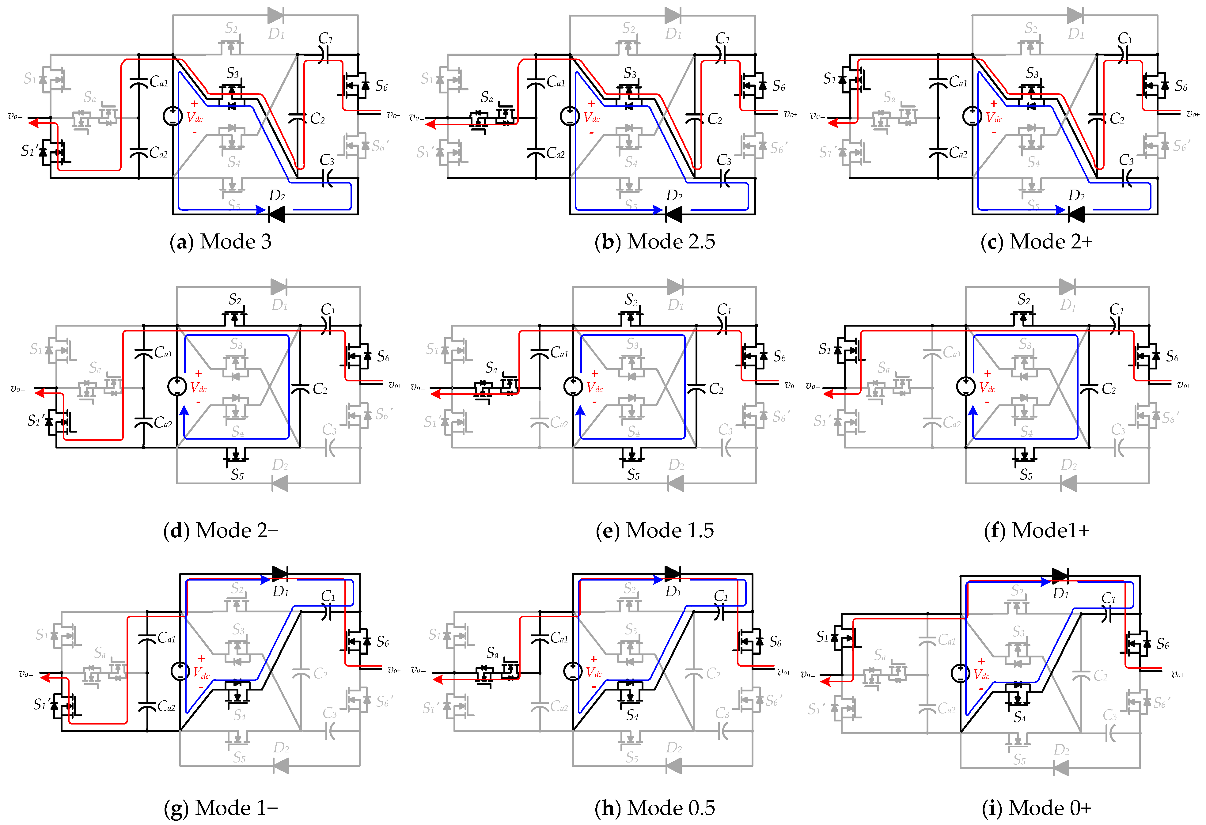
The 13-level inverter has 18 different working modes overall. The information of all the modes is listed in Table 1. Number ‘1’ means the switch is turned on, and ‘0’ means the switch is turned off. In the column of capacitors, ‘C’, ‘D’, and ‘N’ denote charging, discharging, and the isle state, respectively. The switching state for S6′ is complementary to S6, so its states are not listed in the table. It is worthwhile to mention that the output of 2Vdc, Vdc, 0, −Vdc, and −2Vdc all correspond to two different modes, marked with ‘+’ and ‘−’, respectively (for example, mode 2+ and 2− both represent the states generating 2Vdc output). Figure 2 presents information about how the circuit works in a positive half cycle. The red curves in Figure 2 represent the load circuit, and the blue ones show the charging circuit of C1, C2, and C3. The positive working states are analyzed as follows:
(1)
Modes 3, 2.5, and 2+: In these three states, switches S3 and S6 turn on in the high-voltage module. As S3 switches on, the diode D2 is conducted so that the charging loop for C3 is formed. As for the low-voltage module, S1′, Sa, and S1 are switched on in turn to generate 3Vdc, 2.5Vdc, and 2Vdc, respectively.
(2)
Mode 2−, 1.5 and 1+: Similarly, the switching states in the high-voltage module are completely the same, and switches in the low-voltage module are conducted alternately. By turning on S2 and S5, the capacitor C2 can be charged to the input source voltage.
(3)
Mode 1−, 0.5 and 0+: S4 is turned on in these states and D1 conducts so that C1 can be charged to Vdc. As for the low-voltage module, one of three switches is turned on to generate different output levels.
The working principle in the negative half cycle is similar to that in the positive half cycle, so it is not described to avoid repetition.

3. Proposed Modulation Method

In Table 1, it can be seen that the 18 modes are divided into six groups (from A to F). Every group contains three adjacent modes. Coincidentally, in each group, the state of high-voltage module switches (S2,3,3,5,6,6) are completely the same, and low-module switches are conducted by turns. Due to this special characteristic of the working state, a novel hybrid PWM is designed for this inverter.
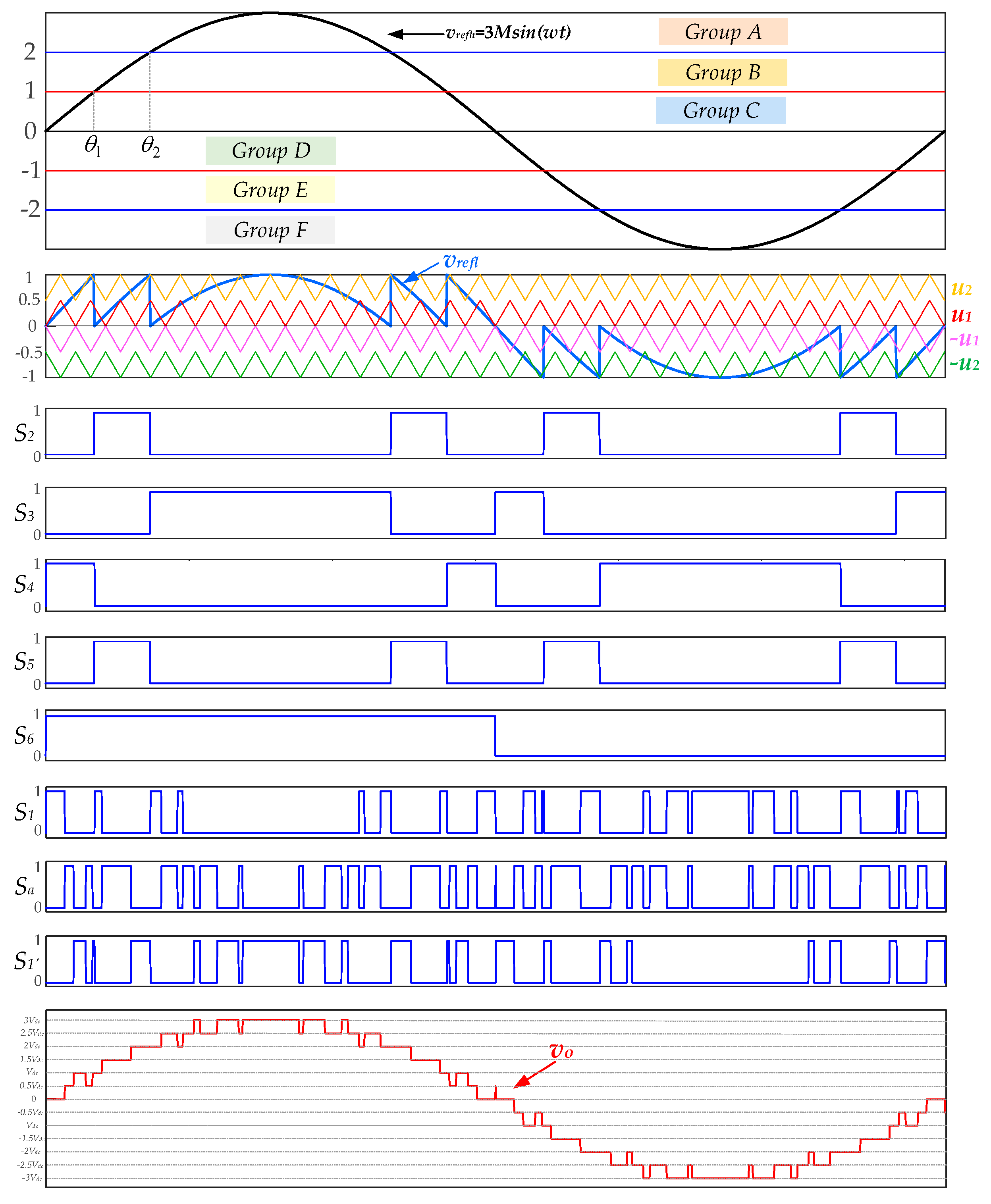
Figure 3 demonstrates the principles of modulation as well as the driving signals of each switch. As is shown in this figure, the high-voltage module and low-voltage module use different modulation types and reference signals.

3.1. Step Waveform Modulation for High-Voltage Module

The high-voltage module uses staircase waveform-based modulation, the reference signal of which is vrefh. The mathematical expression of vrefh is as follows:
v r e f h = 3 M sin ( ω t )
where M is the modulation index and w represents the angular frequency of the output.
As vrefh varies, the switching states of S2 to S6 change according to the rules of grouping. Table 2 gives detailed information on this.

3.2. LS-PWM for Low-Voltage Module

For the low-voltage module, the LS-PWM technique is employed. As is illustrated in Figure 3, the switching states of S1, S1′, and Sa are determined by comparing the low-voltage module reference signal vrefl and four triangular carrier signals: ±u1 and ±u2. The peak-to-peak value of these four carrier signals is 0.5, and the reference signal vrefl can be expressed as Equation (2). The switching signals of S1, Sa, and S1′ follow the rules listed in Table 3.
According to the switching signals in Figure 3, it can be seen that S2~S6 have very low switching frequencies under hybrid modulation. Although S1, S1′, and Sa work in a high-switching frequency state, the blocking voltage at the switching action moment for these three switches is only Vdc/2. Therefore, the hybrid modulation method is able to limit the number of high-frequency switches and reduce the switching loss of this inverter significantly.
v r e f l = v r e f h 2 , v r e f h > 2 v r e f h 1 , 1 < v r e f h < 2 v r e f h , 1 < v r e f h < 1 v r e f h + 1 , 2 < v r e f h < 1 v r e f h + 2 , v r e f h < 2

4. Self-Balance Analysis and Capacitance Calculation

4.1. Self-Balance Analysis

The capacitor’s voltage can be self-balanced under the hybrid modulation technique. The voltage balance for C1, C2, and C3 is achieved by connecting them in parallel with the dc source in different working modes (see Figure 2 or Table 1). Thus, they are charged to Vdc periodically.
The balance principle of Ca1 and Ca2 is based on the neutral point current.
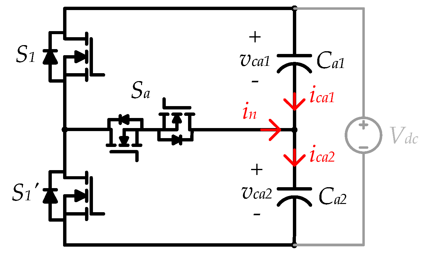
Figure 4 presents the information about the balancing circuit of Ca1 and Ca2. in represents the current flowing into the neutral point, and ica1, ica2 are the currents of the two capacitors. Since these two capacitors are connected with Vdc in parallel, the voltage of the two capacitors vca1 and vca2 must satisfy the following:
v c a 1 + v c a 2 = V d c
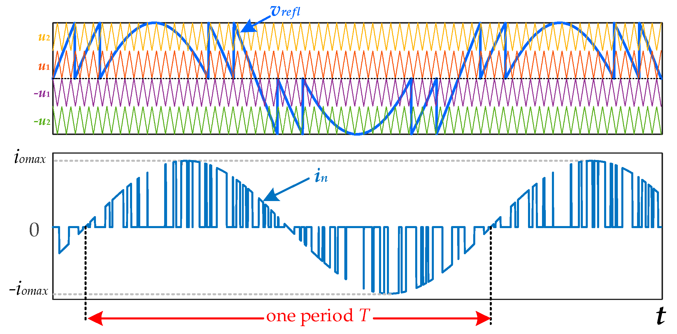
The neutral point current in is equal to the output current io when Sa turns on and becomes zero in other states. Under hybrid modulation, Sa is switched on when u1 < vrefl < u2 or −u2 < vrefl < −u1. To simplify the analysis, we supposed that the output current io was a sinusoidal wave; under this assumption, the waveform of the neutral point current is demonstrated in Figure 5.
In Figure 5, iomax denotes the amplitude of the output current. It is clear that the waveform of in has a central symmetrical characteristic because the conduction period of Sa in the positive and negative half cycle are completely identical. Therefore, the average value of the neutral point current is zero. It is worthwhile to mention that though the output current may not form a pure sinusoidal waveform, the average value is still zero as long as it has symmetrical characteristics. According to Kirchhoff’s circuit laws (KCL), the relationship between in, ica1, and ica2 can be expressed as follows:
i n + i c a 1 = i c a 2
Therefore, the voltage of Ca1 and Ca2 can meet the following expression:
i n + C a 1 d v c a 1 d t = C a 2 d v c a 2 d t
Combining Formulas (3) and (5) and integrating both sides, the voltage fluctuation can be written as follows:
t t + T i n d t = ( C a 1 + C a 2 ) [ v c a 1 ( t + T ) v c a 1 ( t ) ]
where T represents the period of the output voltage. Since the average value of in is 0, we can finally obtain the following:
v c a 1 ( t + T ) = v c a 1 ( t ) v c a 2 ( t + T ) = v c a 2 ( t )
which means that the voltage change in Ca1 and Ca2 during one circle is zero.
Therefore, all the capacitors can achieve self-balance under the novel hybrid modulation method.

4.2. Capacitance Calculation

The calculation principles for capacitor parameters are mainly based on the maximum voltage ripple.
Capacitance calculation for the high-voltage module: To ascertain C1, C2, and C3, it is important to figure out their maximum discharging period. In Figure 3, θ1 and θ2 are switching angles between different groups and can be calculated as follows:
θ i = arcsin ( i 3 M ) i = 1 , 2
where M is the modulation ratio.
For C1, its discharging states are in groups A and B, so its maximum discharging interval is [θ1, π−θ1]. Similarly, the maximum discharging intervals of C2 and C3 are [θ2, π−θ2] and [π + θ1, 2π−θ1], respectively. Of course, when the modulation ratio M is equal to 1, these discharging intervals become the longest. Hence, the maximum voltage ripple for C1, C2, and C3 can be given as follows:
Δ V c 1 = 1 C 1 θ 1 / 2 π f ( π θ 1 ) / 2 π f i o ( t ) d t Δ V c 2 = 1 C 2 θ 2 / 2 π f ( π θ 2 ) / 2 π f i o ( t ) d t Δ V c 1 = 1 C 1 ( π + θ 1 ) / 2 π f ( 2 π θ 1 ) / 2 π f i o ( t ) d t
where ΔVc1, ΔVc2, and ΔVc3 are the maximum voltage ripple of these three capacitors and f is the output frequency. We suppose that the voltage ripple could not exceed 10% of the rated voltage [21]; thus, the selection of capacitance can be given as follows:
C 1 1 10 % × V d c θ 1 / 2 π f ( π θ 1 ) / 2 π f i o ( t ) d t C 2 1 10 % × V d c θ 2 / 2 π f ( π θ 2 ) / 2 π f i o ( t ) d t C 3 1 10 % × V d c ( π + θ 1 ) / 2 π f ( 2 π θ 1 ) / 2 π f i o ( t ) d t
Capacitance calculation for low-voltage module: the current flowing through Ca1 and Ca2 is mainly decided by the neutral point current in. According to (4) and (5), the voltage change in Ca1 can be derived as follows:
1 C a 1 + C a 2 t 1 t 2 i n d t = v c a 2 ( t ) v c a 1 ( t )
where t1 and t2 are two different arbitrary moments.
Therefore, Ca1 has the maximum voltage ripple when the time interval [t1, t2] represents one whole positive half cycle of the output current. Considering the symmetrical structure, we choose the same parameters for Ca1 and Ca2. In order to simplify the calculation, it is supposed that Ca1 discharges during the whole positive half cycle of io. In this way, the maximum voltage ripple of Ca1 is estimated to be:
Δ V c a 1 = 1 2 C a 1 t t + π / ω i o d t = 1 2 C a 1 t t + π / ω 3 M V d c sin ω t Z L d t = 3 M V d c ω C a 1 Z L
where ZL is the load at the output side. When M = 1, the voltage ripple reaches the largest value. If the voltage ripple of Ca1 is no more than 10% of its rated voltage [21], the capacitance for Ca1 and Ca2 can be calculated as follows:
C a 1 = C a 2 60 ω Z L
Actually, the capacitance of Ca1 and Ca2 can be smaller because their discharging time is shorter than half of one cycle during one period. However, to simplify the calculation complexity, Equation (13) is a suitable way to estimate the capacitance.

5. Loss Analysis and Comparative Study

5.1. Loss Analysis

In most cases, the power losses of an SC inverter are mainly caused by conduction loss, the capacitors’ charging loss, and switching loss.
Conduction Loss: The conduction loss of the inverter results from the parasitic parameters of the conducting components in the load circuit, which includes the forward voltage drop in the diode VD, the on-resistance of the diode rD, the on-resistance of the switch rs and the internal resistance of capacitors rC. In order to simplify the calculation, we supposed that the same type of components have identical parameters.
Due to the hybrid modulation method, the conduction losses of the high-voltage module and low-voltage module are calculated separately. For the high-voltage module, the energy losses in the periods of groups A, B, or C during one cycle (which are represented by EconA, EconB, and EconC, respectively) are expressed in (14). The energy losses for groups D, E, and F are the same as A, B, and C.
E c o n A = θ 2 / ω ( π θ 2 ) / ω i o 2 ( 2 r s + 2 r c ) d t E c o n B = θ 1 / ω θ 2 / ω i o 2 ( 2 r s + r c ) d t + ( π θ 1 ) / ω ( π θ 2 ) / ω i o 2 ( 2 r s + r c ) d t E c o n C = 0 θ 1 / ω V D i o + i o 2 ( r s + r D ) d t + ( π θ 1 ) / ω π / ω V D i o + i o 2 ( r s + r D ) d t
where io is the output current. Thus, the conduction losses for the high-voltage module can be calculated as follows:
P c o n H = 2 f o ( E c o n A + E c o n B + E c o n C )
where PconH represents the conduction loss for the high-voltage module and fo represents the output frequency.
As for the low-voltage module, it is assumed that the conducting times of S1, S1′, and Sa take up 1/4, 1/4, and 1/2 of the whole cycle, respectively. Therefore, the conduction loss for the low-voltage module is expressed as follows:
P c o n L = 2 × f o 4 I r m s 2 r s + f o 2 × 2 I r m s 2 r s = 1.5 f o I r m s 2 r s
where Irms is the root mean square value of io
The total conduction loss Pcon is given below:
P c o n = P c o n H + P c o n L
Ripple Loss: The ripple loss is mainly caused by the difference between the ideal capacitor voltage and the actual charging voltage. The estimated ripple loss can be given as follows [16]:
P r i p p l e = f o C a ( Δ V c a ) 2 + 1 2 f o i = 1 3 C i ( Δ V c i ) 2
where ΔVC1, ΔVC2, and ΔVC3 represent the maximum voltage ripple of C1, C2, and C3 and the capacitance value and voltage ripple of Ca1 and Ca2 are assumed to be Ca and ΔVCa.
Switching Loss: Switching loss occurs owing to the time delay when the switch turns on or off. The switching loss of one certain switch Psw can be calculated using Equation (19) [16]:
P s w = f s w C o s s V b 2
where Coss represents the parasitic capacitance of the semiconductor switch and Vb represents the blocking voltage of the power switch at the turning on or turning off moment.
Table 4 presents the blocking voltage, switching frequency, as well as the blocking voltage of each semiconductor switch. In the table, fo represents the output frequency, and fc represents the carrier frequency.
It is worth mentioning that among the six switching actions of S3 and S4 in one output period, two of them have a voltage change of 2Vdc while the voltage changes in the other four is Vdc. This is further verified by experimental results in Section 6.
By adding each switching loss for all the switches in the topology, the total switching loss Psw-tot can be calculated as follows:
P s w t o t = a l l   t h e   s w i t c h e s P s w = ( 40.5 f o + 1 4 f c ) C o s s V d c 2 = ( 162 f o + 2 f c ) C o s s V s t e p 2
where Vstep =Vdc/2 represents the minimum step voltage of the output.

5.2. Comparative Study

Quantitative comparison: To show the merits of the proposed inverter, this part compares the proposed topology with other similar inverters [10,11,14,15,21,23,24,27,28,29,30] in terms of the number of dc sources (NS), switches (Nsw), gate drivers (NDR), diodes (ND), capacitors (NC), levels (Nsw), and the TSV. Considering different boosting abilities, the total standing voltage is calculated as the ratio of the voltage stress of all switches to the minimum step voltage Vstep. Additionally, the cost function (CF) used in [27] is adopted to evaluate the overall performance of the proposed inverter. The CF is expressed as shown in Formula (21):
C F = N s w + N D R + N D + N C + α T S V N l e v e l × N S
where α is the weight coefficient of TSV.
Table 5 gives information about the indexes mentioned above. It is clear that the inverter proposed in [10,11,21] uses two dc sources, and the topology in [29] needs to use three independent sources in one basic unit. Therefore, the CF value in these four papers is higher than the proposed single-source inverters. As for voltage stress, the TSVs of [14,15] are much larger than other inverters because switches in the back-end H bridge withstand the peak output voltage in these two inverters. Among the 13-level inverters, the proposed topology is for the inverter that uses the lowest number of active switches, which is only 10. The CF value of the proposed inverter is almost lower than the other counterparts. The inverter proposed in [30], indeed, has a lower CF value, but it does not have self-balance ability and uses a very complicated method to balance the capacitor voltage, increasing the cost and complexity of the control circuit. Speaking overall, the proposed topology shows superiority over other 13-level inverters.
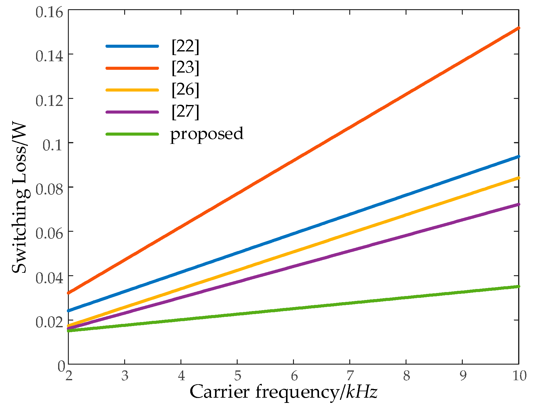
Switching loss comparison: To highlight the feature of hybrid modulation method, a comparative analysis concerning switching loss with other 13-level inverters using high-frequency modulation is demonstrated in this section. The switching losses of the inverters were all calculated using Equation (19). In order to make the comparison fair, it was assumed that all the switches had the same parasitic capacitance, which was 500 pF. And the amplitude of the output voltage was uniformly set to be 300 V, the output frequency was set as 50 Hz, and the load was set to be 80 Ω of pure resistive load.
Figure 6 illustrates the switching loss of different 13-level inverters when the carrier frequency changes from 2 kHz to 10 kHz. It is shown in Figure 6 that the switching loss of the proposed inverter is the lowest in the whole range. Additionally, the slope of the proposed inverter is lowest, which means that the growth rate of switching loss in the proposed inverter is the slowest as carrier frequency increases.

6. Simulation and Experimental Results

6.1. Simulation Results

The proposed inverter was built in PSIM version 9.1.4.400 to verify the feasibility of the topology and modulation. The input voltage Vdc was set as 100 V. The capacitance for Ca1 and Ca2 was 1500 μF, and C1, C2, C3 were chosen to be 2200 μF. The output frequency was 50 Hz, and the carrier wave frequency was 5000 Hz.
Figure 7 demonstrates the output voltage and current under the pure load condition (80 Ω) and inductive load condition (80 Ω + 50 mH), respectively. In Figure 7a, the amplitude of the output voltage vo is 296.67 V, which is close to 300 V. Therefore, the triple boosting ability of the inverter is verified. In Figure 7b, the THD of the output voltage and current are 9.822% and 1.546%, respectively. This shows the filtering property of the inductive load.
Figure 8 illustrates the capacitor voltage of the inverter under 80 Ω load. It can be seen that the voltages of C1, C2, and C3 are maintained at 100 V while voltages of Ca1 and Ca2 are maintained at 50 V. Thus, the self-voltage balance ability of the proposed inverter is proved.

6.2. Experimental Results

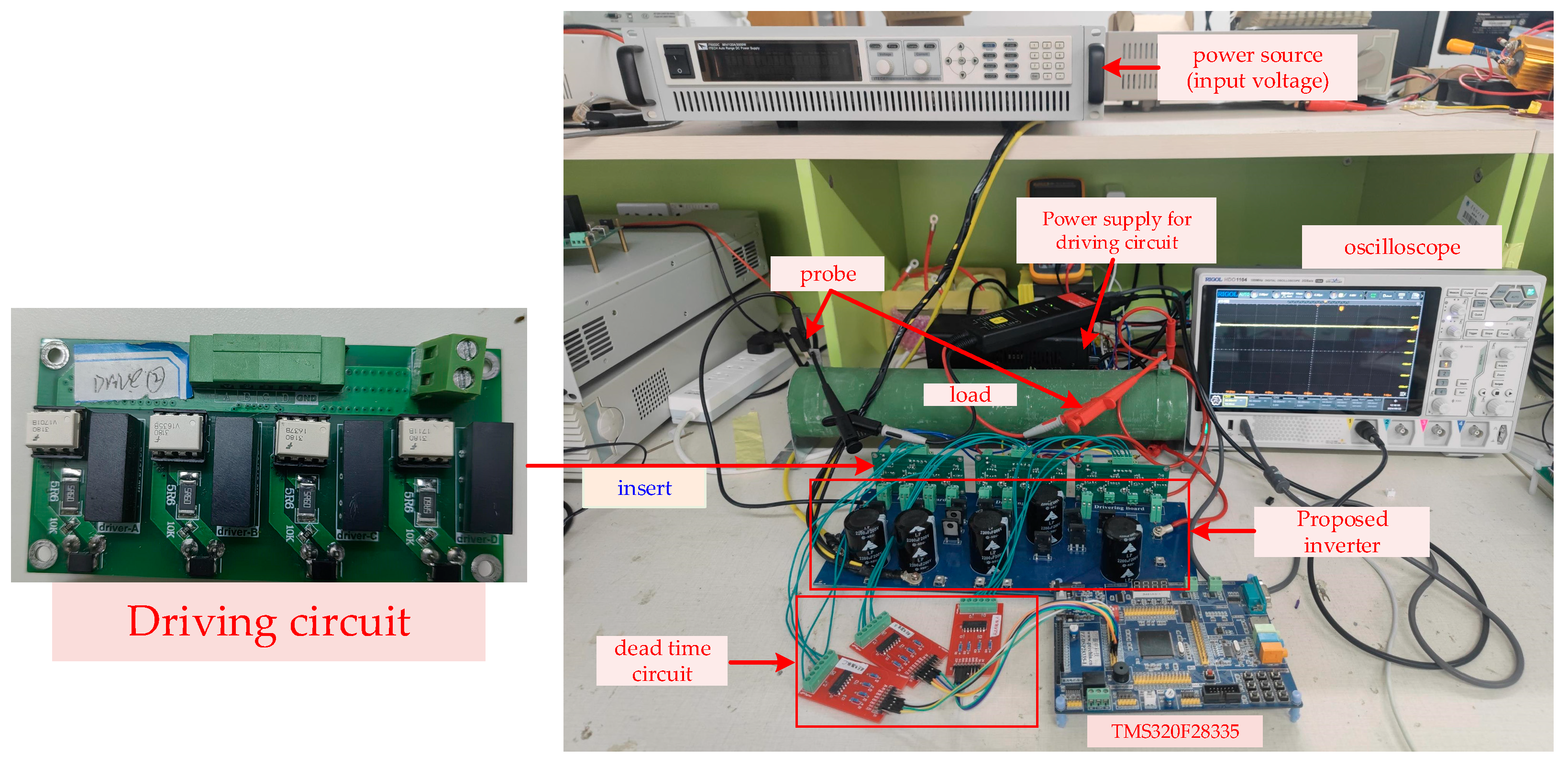
A 13-level inverter laboratory prototype was built in order to further verify the feasibility of the proposed topology and hybrid modulation method. The experimental setup is shown in Figure 9. TMS320F28335 was chosen as the controller, and TLP250 was selected as the gate driver. The dead time for the complementary signals was set at around 170 ns. The power switches and diodes employed CI47N65 and CI30S65D3L2, respectively. Other experimental parameters are listed in Table 6. For S2 and S5, we use MOSFET with body diode in series with a diode to represent because MOSFET with body diode is more common.
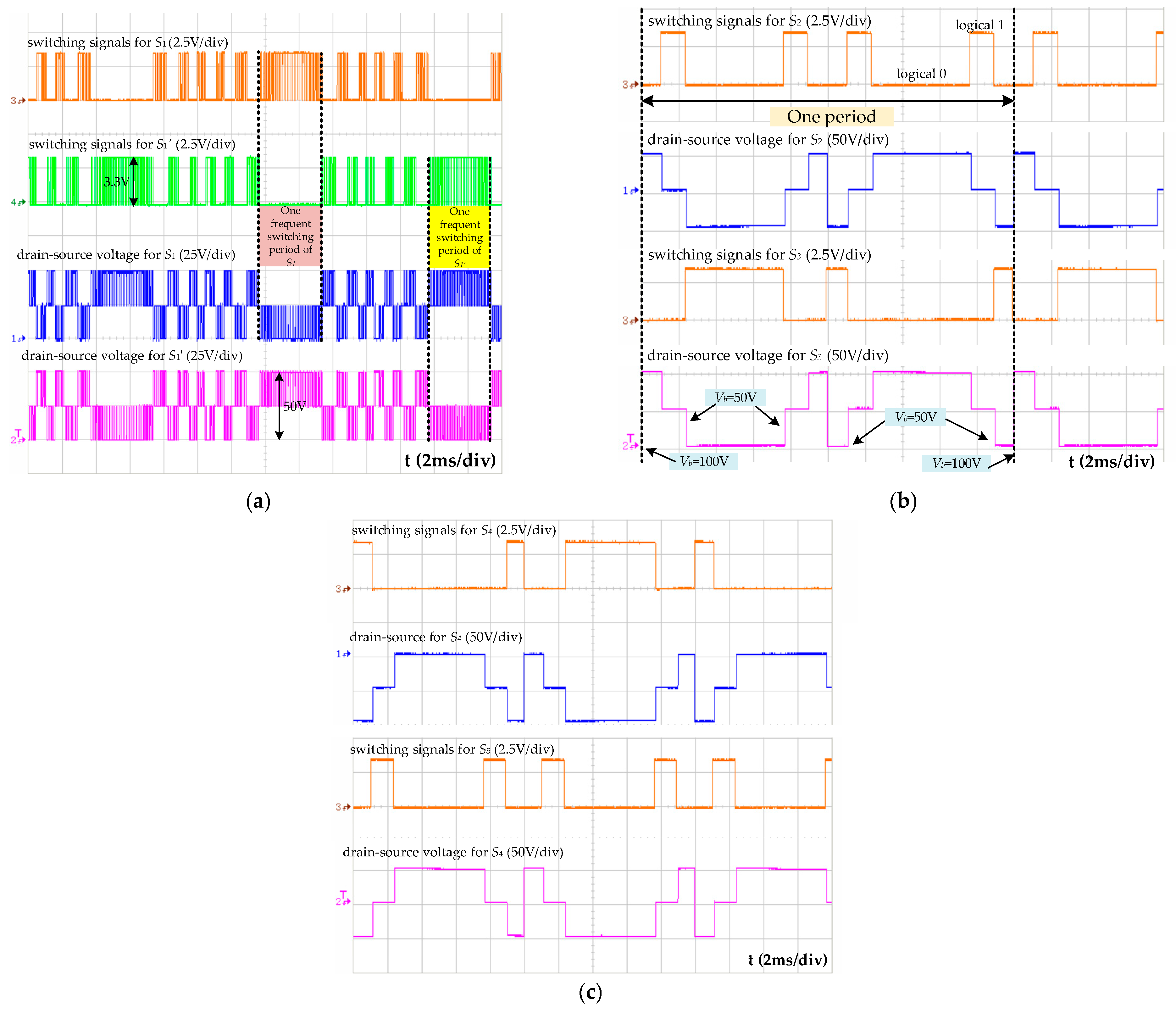
Figure 10 shows the switching signals as well as the drain-source voltage (VDS) of each semiconductor switch under the hybrid modulation method.
As for the switches S1 and S1′, though their maximum voltage stress is Vdc, the blocking voltage before turning on (or after turning off) is only Vdc/2. This can be substantiated by analyzing Figure 10a; for instance, in one of the frequent switching periods, S1, marked in the figure, the voltage changes in S1 is only 25 V. Therefore, the blocking voltage of switches in the low-voltage module is Vdc/2, which is always the minimum step voltage. For S3, it is demonstrated in Figure 10b that among the six switching actions in one period, the blocking voltage of four of them are measured to be 50 V (Vdc), and the remaining two are 100 V (2Vdc). The situation for S4 is completely the same as S3. Therefore, the analysis in the switching loss part in Section 4 is verified.
The switching signals and drain-source voltage waveforms in Figure 10 prove that switches in the high-voltage module all work in a low-frequency state under the hybrid modulation method. Therefore, this hybrid modulation limits the number of high-frequency switches and reduces the switching loss significantly.
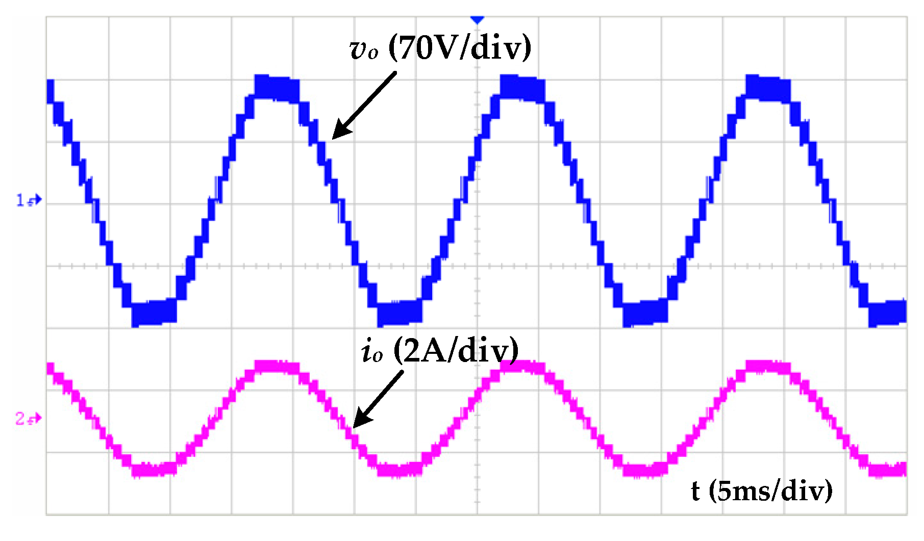
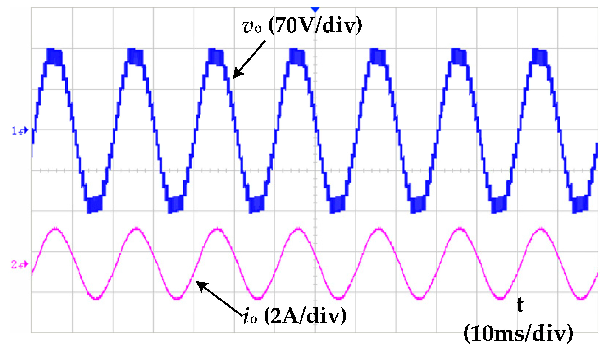
Figure 11 depicts the output waveforms of the voltage vo and current io under an 80 Ω load. The modulation ratio M was set to unity. The amplitude of the output voltage was 142.8 V, which is lower than the theoretical value because of the conduction forward voltage of the switches and diodes. The root mean square (rms) value of io was measured to be 1.27 A. The capacitors’ voltage waveforms, as well as the ripple, are shown in Figure 12. It is clear that the voltages of Ca1 and Ca2 are maintained at 25 V, and C1, C2, and C3 are kept at 50 V, so the self-balance capability of the proposed inverter is verified. The voltage ripple of Ca1 and Ca2 is less than 2 V, and the figure for other three capacitors shows a value less than 2.5 V; hence, all the capacitor voltage ripples are less than 10% of their rated voltage.
Figure 13 depicts the waveforms of the output voltage and current with an 80 Ω + 28 mH load. The peak output of the current is 1.76 A. Thus, this inverter has the ability to drive inductive load.
To explore how the modulation ratio M influences the output, the proposed inverter is tested with M = 0.7, M = 0.5, and M = 0.3 (under an 80 Ω + 28 mH load), respectively. The results are shown in Figure 14. It can be seen that as the modulation ratio reduces, the levels of the inverter decrease. The number of output levels becomes 11, 7, and 5, respectively.
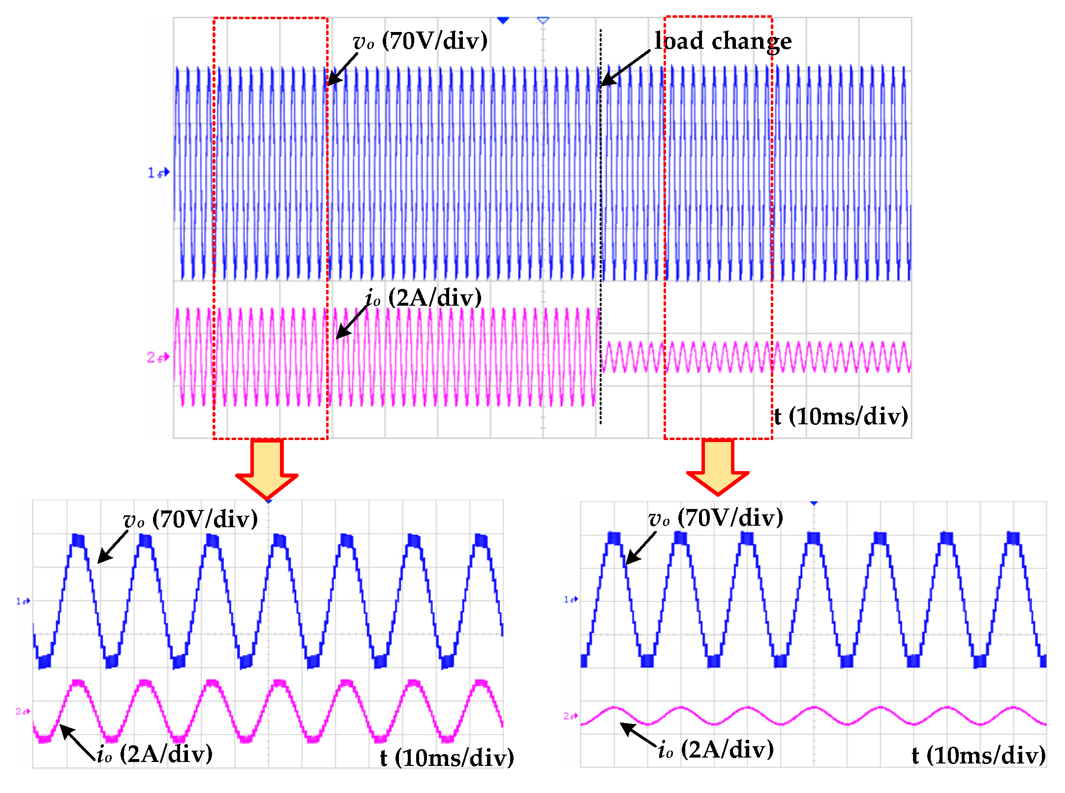
A load change experiment was carried out to examine the transient response of the proposed inverter. Figure 15 illustrates the output waveforms under the condition of a sudden load change from 80 Ω to 280 Ω + 46 mH. It is clearly demonstrated in the figure that at the load change moment, the output voltage is basically uninfluenced while the amplitude of output current dramatically decreases. The RMS values of the current before and after the load change are 1.2698 A and 356.36 mA, respectively. After some time has passed from the load change, io becomes a sinusoidal waveform, and the output reaches its steady state again. Therefore, the proposed topology has a good transient response performance under the proposed novel hybrid modulation method.

7. Conclusions

A 13-level inverter, based on an SC technique, is proposed in this paper. The proposed topology has the advantage of a low switch count, self-voltage balance, no back-end H bridge, and triple boosting ability. Owing to its unique switching states, a novel hybrid modulation method can be applied to this inverter. By using the hybrid modulation method, the switches in the high-voltage module all work in low-frequency states, and their switching frequencies are not affected by the frequency of triangular carrier waves. As a result, the switching loss is significantly reduced. The comparison results highlight the merit of the proposed topology and modulation method. And simulation and experimental results verified the feasibility of the proposed inverter. The proposed inverter can be modulated both by HFM and FFM. Therefore, it can be applied in power-frequency occasions such as distributed generation power systems. It can also be used in high-frequency occasions by using FFM, such as a high-frequency AC system or wireless power transfer.

Author Contributions

Conceptualization, Z.W. and Y.L.; methodology, Z.W. and Y.L.; resources, T.L. and J.L.; data curation, M.F. and C.H.; writing—original draft, Z.W.; writing—review and editing, Z.W.; supervision, T.L. and J.L.; project administration, Z.W. All authors have read and agreed to the published version of the manuscript.

Funding

This research was funded by the Science and Technology Project of the China Southern Power Grid (No. 080036KK52210003).

Data Availability Statement

Data are available upon request due to restrictions.

Conflicts of Interest

Authors Zhipeng Wu, Yuanhuang Liu, Tianchu Li and Ming Fang are employed by the Hainan Power Grid Co., Ltd., while author Chunyan Huang is employed by Guangzhou Power Electrical Technology Co., Ltd. The remaining author declares that the research was conducted in the absence of any commercial or financial relationships that could be construed as a potential conflict of interest.

References

  1. Hsieh, C.-H.; Liang, T.-J.; Chen, S.-M.; Tsai, S.-W. Design and Implementation of a Novel Multilevel DC–AC Inverter. IEEE Trans. Ind. Appl. 2016, 52, 2436–2443. [Google Scholar] [CrossRef]
  2. Xiao, B.; Hang, L.; Mei, J.; Riley, C.; Tolbert, L.M.; Ozpineci, B. Modular Cascaded H-Bridge Multilevel PV Inverter with Distributed MPPT for Grid-Connected Applications. IEEE Trans. Ind. Appl. 2015, 51, 1722–1731. [Google Scholar] [CrossRef]
  3. Sheir, A.; Youssef, M.Z.; Orabi, M.A. Novel Bidirectional T-Type Multilevel Inverter for Electric Vehicle Applications. IEEE Trans. Power Electron. 2019, 34, 6648–6658. [Google Scholar] [CrossRef]
  4. Yu, Y.; Konstantinou, G.; Hredzak, B.; Agelidis, V.G. Power Balance of Cascaded H-Bridge Multilevel Converters for Large-Scale Photovoltaic Integration. IEEE Trans. Power Electron. 2016, 31, 292–303. [Google Scholar] [CrossRef]
  5. Ye, Z.; Lei, Y.; Liao, Z.; Pilawa-Podgurski, R.C.N. Investigation of Capacitor Voltage Balancing in Practical Implementations of Flying Capacitor Multilevel Converters. IEEE Trans. Power Electron. 2022, 37, 2921–2935. [Google Scholar] [CrossRef]
  6. Guo, X.; Cavalcanti, M.C.; Farias, A.M.; Guerrero, J.M. Single-Carrier Modulation for Neutral-Point-Clamped Inverters in Three-Phase Transformerless Photovoltaic Systems. IEEE Trans. Power Electron. 2013, 28, 2635–2637. [Google Scholar] [CrossRef]
  7. Iqbal, A.; Siddique, M.D.; Reddy, B.P.; Maroti, P.K. Quadruple Boost Multilevel Inverter (QB-MLI) Topology With Reduced Switch Count. IEEE Trans. Power Electron. 2022, 36, 7372–7377. [Google Scholar] [CrossRef]
  8. Akbari, A.; Ebrahimi, J.; Jafarian, Y.; Bakhshai, A. A Multilevel Inverter Topology with an Improved Reliability and a Reduced Number of Components. IEEE J. Emerg. Sel. Top. Power Electron. 2022, 10, 553–563. [Google Scholar] [CrossRef]
  9. Samadaei, E.; Sheikholeslami, A.; Gholamian, S.A.; Adabi, J. A Square T-Type (ST-Type) Module for Asymmetrical Multilevel Inverters. IEEE Trans. Power Electron. 2018, 33, 987–996. [Google Scholar] [CrossRef]
  10. Roy, T.; Sadhu, P.K.; Dasgupta, A. Cross-Switched Multilevel Inverter Using Novel Switched Capacitor Converters. IEEE Trans. Ind. Electron. 2019, 66, 8521–8532. [Google Scholar] [CrossRef]
  11. Samadaei, E.; Kaviani, M.; Bertilsson, K. A 13-Levels Module (K-Type) With Two DC Sources for Multilevel Inverters. IEEE Trans. Ind. Electron. 2019, 66, 5186–5196. [Google Scholar] [CrossRef]
  12. Zhang, Y.; Wang, Q.; Hu, C.; Shen, W.; Holmes, D.G.; Yu, X. A Nine-Level Inverter for Low-Voltage Applications. IEEE Trans. Power Electron. 2020, 35, 1659–1671. [Google Scholar] [CrossRef]
  13. Liu, J.; Wu, J.; Zeng, J.; Guo, H. A Novel Nine-Level Inverter Employing One Voltage Source and Reduced Components as High-Frequency AC Power Source. IEEE Trans. Power Electron. 2017, 32, 2939–2947. [Google Scholar] [CrossRef]
  14. Ye, Y.; Cheng, K.W.E.; Liu, J.; Ding, K. A Step-Up Switched-Capacitor Multilevel Inverter with Self-Voltage Balancing. IEEE Trans. Ind. Electron. 2014, 61, 6672–6680. [Google Scholar] [CrossRef]
  15. Zeng, J.; Wu, J.; Liu, J.; Guo, H. A Quasi-Resonant Switched-Capacitor Multilevel Inverter with Self-Voltage Balancing for Single-Phase High-Frequency AC Microgrids. IEEE Trans. Ind. Inform. 2017, 13, 2669–2679. [Google Scholar] [CrossRef]
  16. Zeng, J.; Lin, W.; Cen, D.; Liu, J. Novel K-Type Multilevel Inverter with Reduced Components and Self-Balance. IEEE J. Emerg. Sel. Top. Power Electron. 2020, 8, 4343–4354. [Google Scholar] [CrossRef]
  17. Wang, Y.; Wang, C.; Guo, Y.; Wang, K.; Liang, J. An X-type Boost Multilevel Inverter Based on Switched Capacitor Cells with Low Voltage Stress and High Frequency Applications. IEEE J. Emerg. Sel. Top. Power Electron. 2021, 11, 3623–3632. [Google Scholar] [CrossRef]
  18. Lee, S.S.; Bak, Y.; Kim, S.-M.; Joseph, A.; Lee, K.-B. New Family of Boost Switched-Capacitor Seven-Level Inverters (BSC7LI). IEEE Trans. Power Electron. 2019, 34, 10471–10479. [Google Scholar] [CrossRef]
  19. Alyami, S.; Ali, J.S.M.; Almakhles, D.; Almutairi, A.M. Obeidat. Seven Level T-Type Switched Capacitor Inverter Topology for PV Applications. IEEE Access 2021, 9, 85049–85059. [Google Scholar] [CrossRef]
  20. Lee, S.S. Single-Stage Switched-Capacitor Module (S3CM) Topology for Cascaded Multilevel Inverter. IEEE Trans. Power Electron. 2018, 33, 8204–8207. [Google Scholar] [CrossRef]
  21. Liu, J.; Cheng, K.W.E.; Ye, Y. A Cascaded Multilevel Inverter Based on Switched-Capacitor for High-Frequency AC Power Distribution System. IEEE Trans. Power Electron. 2014, 29, 4219–4230. [Google Scholar] [CrossRef]
  22. Roy, T.; Sadhu, P.K. A Step-Up Multilevel Inverter Topology Using Novel Switched Capacitor Converters with Reduced Components. IEEE Trans. Ind. Electron. 2021, 68, 236–247. [Google Scholar] [CrossRef]
  23. Lin, W.; Zeng, J.; Liu, J.; Yan, Z.; Hu, R. Generalized Symmetrical Step-Up Multilevel Inverter Using Crisscross Capacitor Units. IEEE Trans. Ind. Electron. 2020, 67, 7439–7450. [Google Scholar] [CrossRef]
  24. Anand, V.; Singh, V. A 13-Level Switched-Capacitor Multilevel Inverter with Single DC Source. IEEE J. Emerg. Sel. Top. Power Electron. 2022, 10, 1575–1576. [Google Scholar] [CrossRef]
  25. Bhatnagar, P.; Singh, A.K.; Gupta, K.K.; Siwakoti, Y.P. A Switched-Capacitors-Based 13-Level Inverter. IEEE Trans. Power Electron. 2022, 37, 644–658. [Google Scholar] [CrossRef]
  26. Ye, Y.; Chen, S.; Zhang, X.; Yi, Y. Half-Bridge Modular Switched-Capacitor Multilevel Inverter with Hybrid Pulsewidth Modulation. IEEE Trans. Power Electron. 2020, 35, 8237–8247. [Google Scholar] [CrossRef]
  27. Ye, Y.; Chen, S.; Wang, X.; Cheng, K.-W.E. Self-Balanced 13-Level Inverter Based on Switched Capacitor and Hybrid PWM Algorithm. IEEE Trans. Ind. Electron. 2021, 68, 4827–4837. [Google Scholar] [CrossRef]
  28. Ye, Y.; Zhang, G.; Wang, X.; Yi, Y.; Cheng, K.W.E. Self-Balanced Switched-Capacitor Thirteen-Level Inverters with Reduced Capacitors Count. IEEE Trans. Ind. Electron. 2022, 69, 1070–1076. [Google Scholar] [CrossRef]
  29. Boora, K.; Kumar, J. A Novel Cascaded Asymmetrical Multilevel Inverter with Reduced Number of Switches. IEEE Trans. Ind. Appl. 2019, 55, 7389–7399. [Google Scholar] [CrossRef]
  30. Laib, A.; Krama, A.; Sahli, A.; Kihal, A.; Abu-Rub, H. Reconfigurable Model Predictive Control for Grid Connected PV Systems Using Thirteen-Level Packed E-Cell Inverter. IEEE Access 2022, 10, 102210–102222. [Google Scholar] [CrossRef]
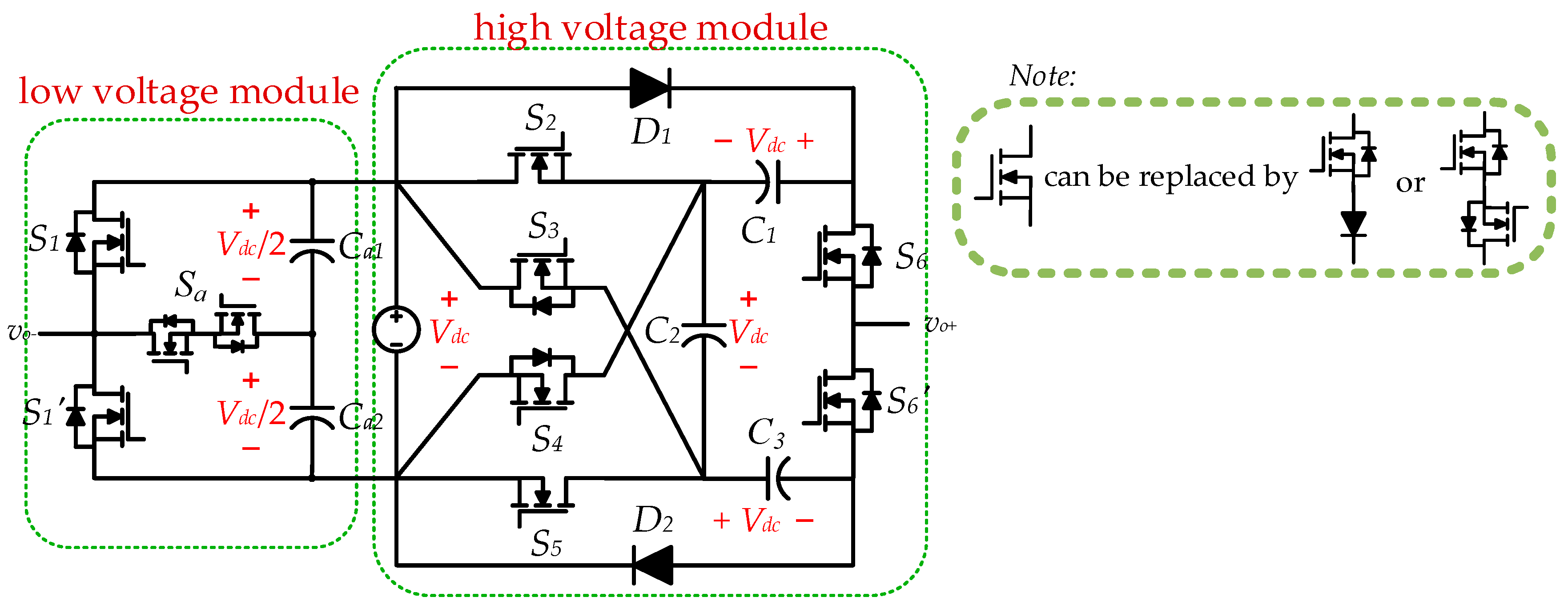
Figure 1. Proposed 13-level topology.
Energies 17 05104 g001
Figure 2. Load and charging circuit for positive half cycle. (a) vo = 3Vdc. (b) vo = 2.5Vdc. (c,d) vo = 2Vdc. (e) vo = 1.5Vdc. (f) and (g) vo = Vdc. (h) vo = 0.5Vdc. (i) vo = 0.
Energies 17 05104 g002
Figure 3. Illustrations of the hybrid modulation method and driving signals of switches.
Energies 17 05104 g003
Figure 4. Voltage and current analysis of low-voltage module.
Energies 17 05104 g004
Figure 5. Waveform of neutral point current in.
Energies 17 05104 g005
Figure 6. Comparison results of switching loss.
Energies 17 05104 g006
Figure 7. Simulated results of output voltage and current under (a) 80 Ω; (b) 80 Ω + 50 mH.
Energies 17 05104 g007
Figure 8. Capacitor voltage of (a) Ca1 and Ca2; (b) C1, C2 and C3.
Energies 17 05104 g008
Figure 9. Experimental setup.
Energies 17 05104 g009
Figure 10. Switching signals and drain-source voltage for (a) S1 and S1′, (b) S2 and S3, and (c) S4 and S5.
Energies 17 05104 g010
Figure 11. Output voltage and current with an 80 Ω resistive load.
Energies 17 05104 g011
Figure 12. Capacitor voltage and ripples of (a) Ca1, Ca2; (b) C1, C2, C3.
Energies 17 05104 g012
Figure 13. Output voltage and current under an 80 Ω + 28 mH inductive load.
Energies 17 05104 g013
Figure 14. Output voltage and current with (a) M = 0.7, (b) M = 0.5, and (c) M = 0.3.
Energies 17 05104 g014
Figure 15. Output waveforms under a load change from 80 Ω to 280 Ω + 46 mH.
Energies 17 05104 g015
Table 1. Switching state of proposed 13-level inverter.
GroupModeS1SaS1S2,3,4,5,6C1C2C3vo
A3001 3Vdc
2.501001001DDC2.5Vdc
2+100 2Vdc
B2−001 2Vdc
1.501010011DCN1.5Vdc
1+100 Vdc
C1−001 Vdc
0.501000101CNN0.5Vdc
0+100 0
D0−001 0
−0.501001000NNC−0.5Vdc
(−1)+100 Vdc
E(−1)−001 Vdc
−1.501010010NCD−1.5Vdc
(−2)+100 −2Vdc
F(−2)−001 −2Vdc
−2.501000100CDD−2.5Vdc
−3100 −3Vdc
Table 2. Modulation state for high-voltage module.
StateGroupS2,3,4,5,6
vrefh > 2A01001
1 < vrefh < 2B10011
0 < vrefh < 1C00101
−1 < vrefh < 0D01000
−2 < vrefh < −1E10010
vrefh < −2F00100
Table 3. Modulation states for low-voltage module.
StateS1 Sa S1
vrefl > u2001
u1 < vrefl < u2010
0 < vrefl < u1100
u1 < vrefl < 0001
u2 < vrefl < −u1010
vrefl < −u2100
Table 4. Switching frequency and blocking voltage of various switches.
SwtichesSwitching FrequencyBlocking Voltage
S1 and S15fo + fc/2Vdc/2
SafcVdc/2
S2 and S54foVdc
S3 and S43fo2Vdc, Vdc
S6 and S6fo3Vdc
Table 5. Quantitative comparison with similar topology.
ReferenceNsNswNDRNDNCNlevelTSVVstep)H BridgeCF
α = 0.5α = 1α = 1.5
[10]21616241334No8.4611.0813.69
[11]21411021339No7.1510.1513.15
[14]11081051359Yes4.817.089.35
[15]1146661348Yes4.316.258
[27]11010441336No3.544.926.31
[28]11212431336No3.765.156.53
[21]21414241336No810.7713.54
[24]11515031335No3.885.236.58
[23]11918041340No4.696.237.77
[29]
(one basic unit)
388001728No5.297.7610.23
[30]1108041328No33.844.92
Proposed1108451337No3.54.926.34
Table 6. Experimental parameters.
ItemsValue
Input voltage Vdc50 V
Capacitance2200 μF
Output frequency fo50 Hz
Carrier wave frequency10 kHz
Disclaimer/Publisher’s Note: The statements, opinions and data contained in all publications are solely those of the individual author(s) and contributor(s) and not of MDPI and/or the editor(s). MDPI and/or the editor(s) disclaim responsibility for any injury to people or property resulting from any ideas, methods, instructions or products referred to in the content.