1. Introduction
Recently, the storage of renewable energy has become an important issue [
1,
2,
3,
4,
5,
6,
7,
8,
9,
10,
11,
12,
13,
14,
15]. To store this energy, supercapacitors are important due to their large power density, which is 10 times larger than that of lithium-ion batteries [
1,
3,
9]. Moreover, their operating temperature has a wider range [
3]. The lifetime of supercapacitors is 1,000,000 cycles [
4], while that of lithium-ion batteries is about 5000 cycles [
5,
6], and their energy density is currently about 17 Wh/kg [
2], which is 20% that of iron phosphate lithium-ion batteries at 100 Wh/kg [
7]. However, this energy density is not a serious problem when they are used in a sufficiently wide space. These advantageous characteristics make supercapacitors very suitable for storing energy from renewable resources. However, there is a problem in that the energy-stored capacitor voltage decreases when a supercapacitor is discharged. Therefore, a step-up circuit is usually used to maintain the output voltage. However, the discharging method with a step-up circuit is not the only one that uses two supercapacitors. Another method uses capacitors that are connected in parallel during charging and in series during discharging. With this series–parallel conversion method [
16,
17], the capacitor voltage becomes two times larger during discharging; thus a step-down circuit can be used to produce the desired output voltage. In this paper, we investigate which method, the step-up or step-down method, is better from the viewpoint of power efficiency.
2. Theoretical Analysis
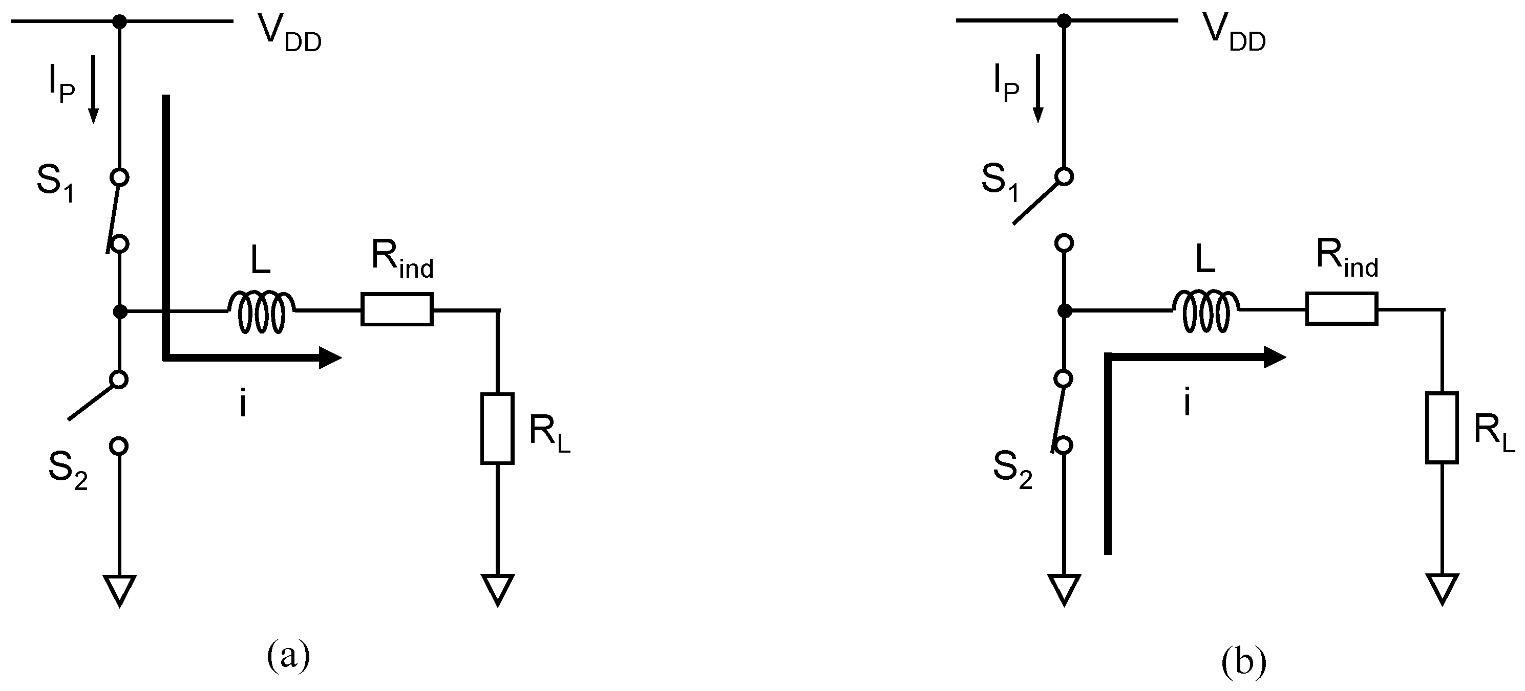
Figure 1 shows a step-down circuit, which has two switching transistors (
and
), an inductor, and a load resistor
[
18,
19]. The power supply voltage is
. The
and
transistors are turned on alternately. The inductor has inductance
L and resistance
. The switching transistor is set to be ideal like a mechanical switch, and the on-resistance in the transistor is
. The ratio between the time when
is ON and a period is defined as the duty ratio
d. Then, the output voltage
is equal to
. The inductor current
i is almost constant in the steady state.
Figure 2 shows a step-up circuit, which has two switching transistors (
and
), an inductor, a capacitor, and a load resistor. The inductor has inductance
L and resistance
. Similar to the step-down circuit, the ratio between the time when
is ON and a period is defined as
d. In this circuit, the output voltage is equal to
. When
or
is turned on, the inductor current
i flows as shown in
Figure 2a or
Figure 2b, respectively. The current
i is also almost constant in the steady state. Here, the current through the load resistor
is investigated. The current through the capacitor in
Figure 2a is defined as
. The direction of the current flowing from the top to the bottom of the capacitor is defined as positive. From the current law, we have
Next, we consider the current law in
Figure 2b. The current through the capacitor in
Figure 2b is defined as
. The positive direction is the same as from top to bottom. Then, we have
in
Figure 2b. Using the law of charge conservation at the capacitor, we have:
The value of
is equal to the charge amount from the power supply to the capacitor when
is ON, and
is equal to the charge amount from the capacitor to the load resistor when
is ON. Therefore, using (1), we have:
Therefore, we have the following relationship in the circuit shown in
Figure 2:
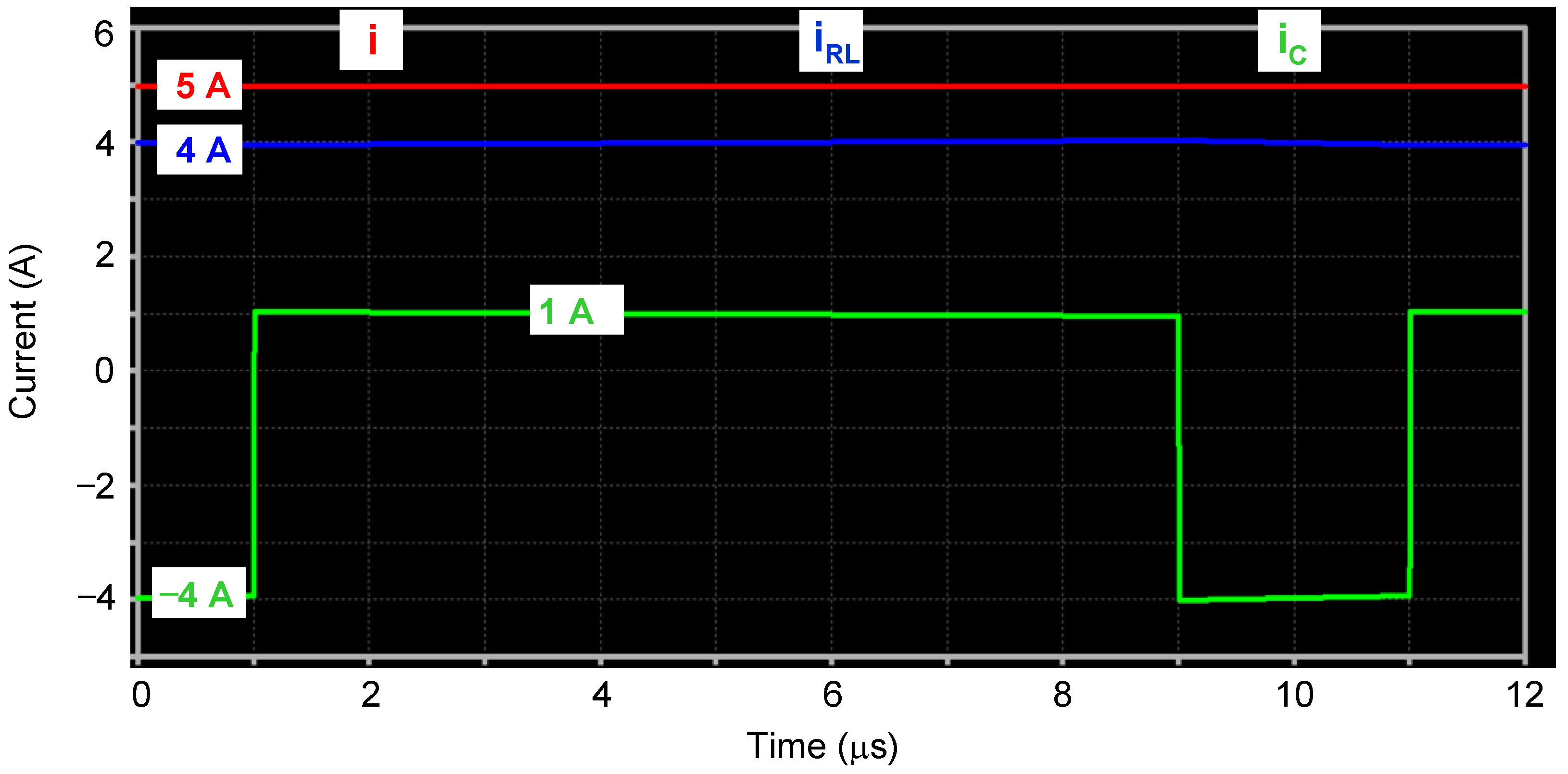
This relationship was confirmed in SPICE simulations, as shown in
Figure 3. In the simulation,
i was a constant 5 A and
d was 0.8. Then,
was equal to 4 A. When
was ON (1 ≦
t ≦ 9 μs),
was 1 A. During this time,
was satisfied. When
was ON (9 ≦
t ≦ 11 μs),
was −4 A.
The relationship was also satisfied during this time. From the simulation, the described equation could be confirmed.
Next, the energy efficiency of the step-down circuit
was considered. The current trough load resistor is a constant
i. Then, the output power
is
. The input power
is the sum of the power consumption of
,
, and
. Then,
is derived as
and written as:
The energy efficiency of the step-up circuit
can be calculated in the same way. This time, the current trough load resistor is written as
di from (4). Then,
is derived as:
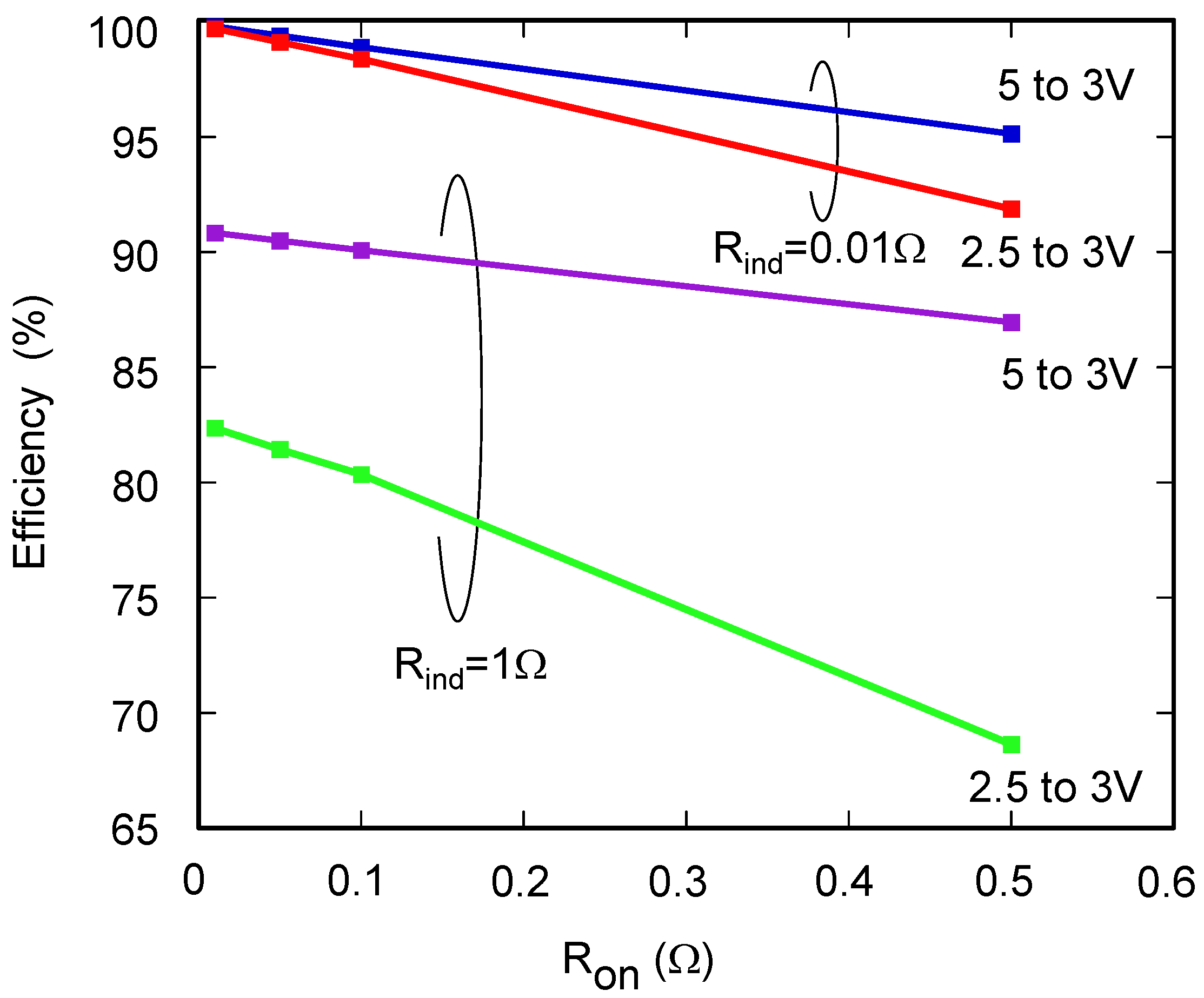
Next, we investigated the energy efficiency in a SPICE simulation. During the step-down simulation, the power supply voltage was set to 5 V and the output voltage was 3 V. During the step-up simulation, the power supply voltage was set to 2.5 V and increased to 3 V.
L was set as 1 H.
was set as 1 or 0.01 Ω.
was set as 10 Ω.
was changed, with values of 0.01, 0.05, 0.1, and 0.5 Ω. On the other hand, the value of the off-resistance in the transistor was 10 MΩ. The power efficiency was calculated as
in SPICE. The simulation and analytical results of
and
from (5) and (6) are shown in
Table 1 and
Table 2, respectively. They were perfectly consistent with each other. For a clear understanding of the dependence of
, the simulation results are shown in
Figure 4. The graph shows that the step-down circuit exhibits better efficiency than the step-up circuit.
The efficiencies increased when the resistance values ( and ) decreased. When both and were 0.01 Ω, the efficiency reached almost 100%.
Next, the dependence of
was investigated. The values of
and
were set to 0.01 and 0.05 Ω, respectively.
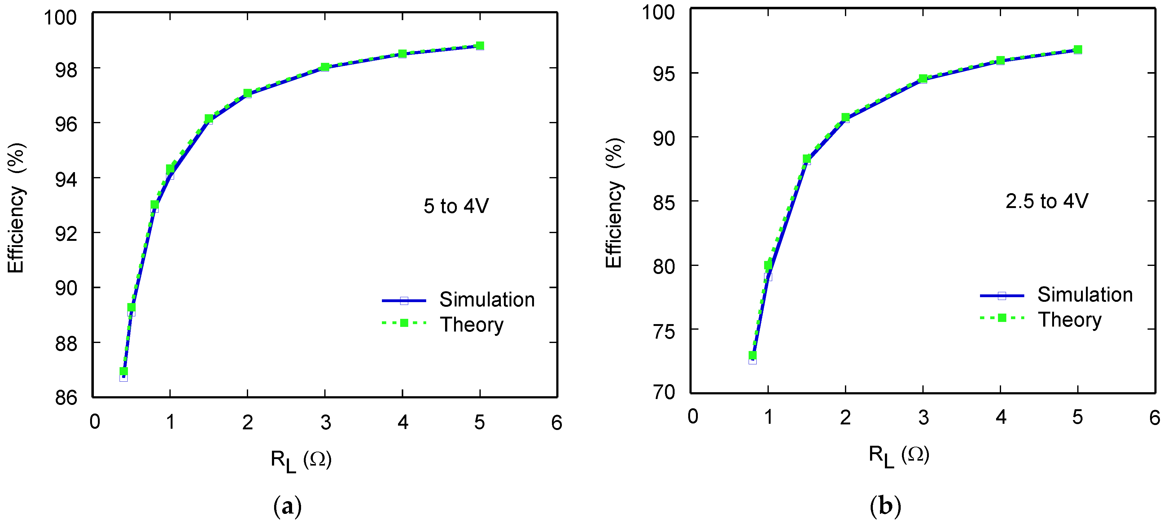
Figure 5a shows the efficiency of the step-down circuit as a function of
when the power supply voltage of 5 V was reduced to an output voltage of 4 V. The simulation and theoretical results are shown as solid and dashed lines, respectively, and they were extremely consistent with one another.
Figure 5b shows the efficiency of the step-up circuit when the power supply voltage of 2.5 V was increased to the same output voltage of 4 V. The simulation and theoretical values are shown as solid and dashed lines, respectively. They agreed well with one another. When
0.8 Ω, the efficiencies of the step-down and step-up circuits were 93 and 72%, respectively. These efficiencies meant that the energy loss decreased to 1/4. This result shows that the step-down circuit is superior to the step-up circuit for producing the same output voltage of 4 V.
Figure 6 shows the simulation results of the efficiencies of the step-down and step-up circuits as a function of
with two output voltages of 3 and 4 V. Regarding the step-down circuit, the power supply voltage was set to 5 V. The efficiencies from 5 to 3 V and from 5 to 4 V were consistent with one another. This is well understood using (5). Equation (5) does not include
d, which means that
is not dependent on
d. In other words,
is not dependent on the output voltage. Therefore, whether the output voltage was 3 or 4 V,
had the same value when
was the same.
Regarding the step-up circuit, the power supply voltage was set to 2.5 V. The simulated efficiency from 2.5 to 4 V was much lower than that from 2.5 to 3 V. This was due to the fact that (6) includes d, which means that is dependent on d. When the output voltage increases, d is decreased via the relationship . Therefore, it is understood from (6) that the theoretical efficiency becomes smaller when the output voltage increases.
3. Experimental Results
Next, the experimental efficiency was measured with a breadboard. Regarding the step-down circuit, a pMOS transistor (2SJ438) and a diode (2GWJ42) were used for and . As an inductor, a toroidal coil of 100 μH was used. The values of were 12, 20, and 50 Ω. The power supply voltage was 18 V and decreased to an output voltage of 12 V.
Regarding the step-up circuit, the same diode and an nMOS transistor (2SK2231) were used for and . The same toroidal coil was used as the inductor. As the capacitor, an aluminum electrolytic capacitor was used, where C was 100 μF. The power supply voltage was 8 V and was increased to the same output voltage of 12 V.
To turn the MOS transistor on, a pulse width modulation (PWM) signal was used, which was produced from a microprocessor (PIC16F627A). Using the PIC, the value of
d of the pulse could be changed digitally.
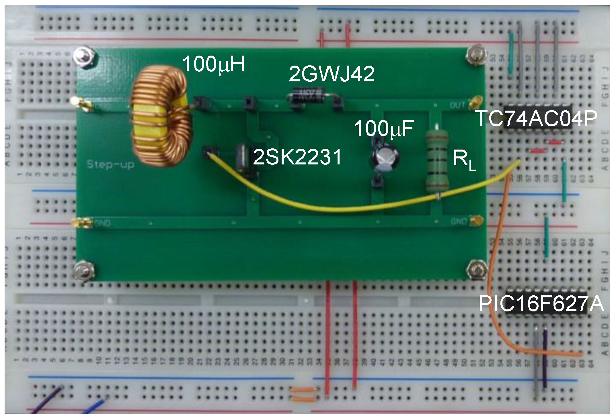
Figure 7 shows the experimental step-up circuit with a breadboard. In the circuit, the diode and the nMOS transistor were used.
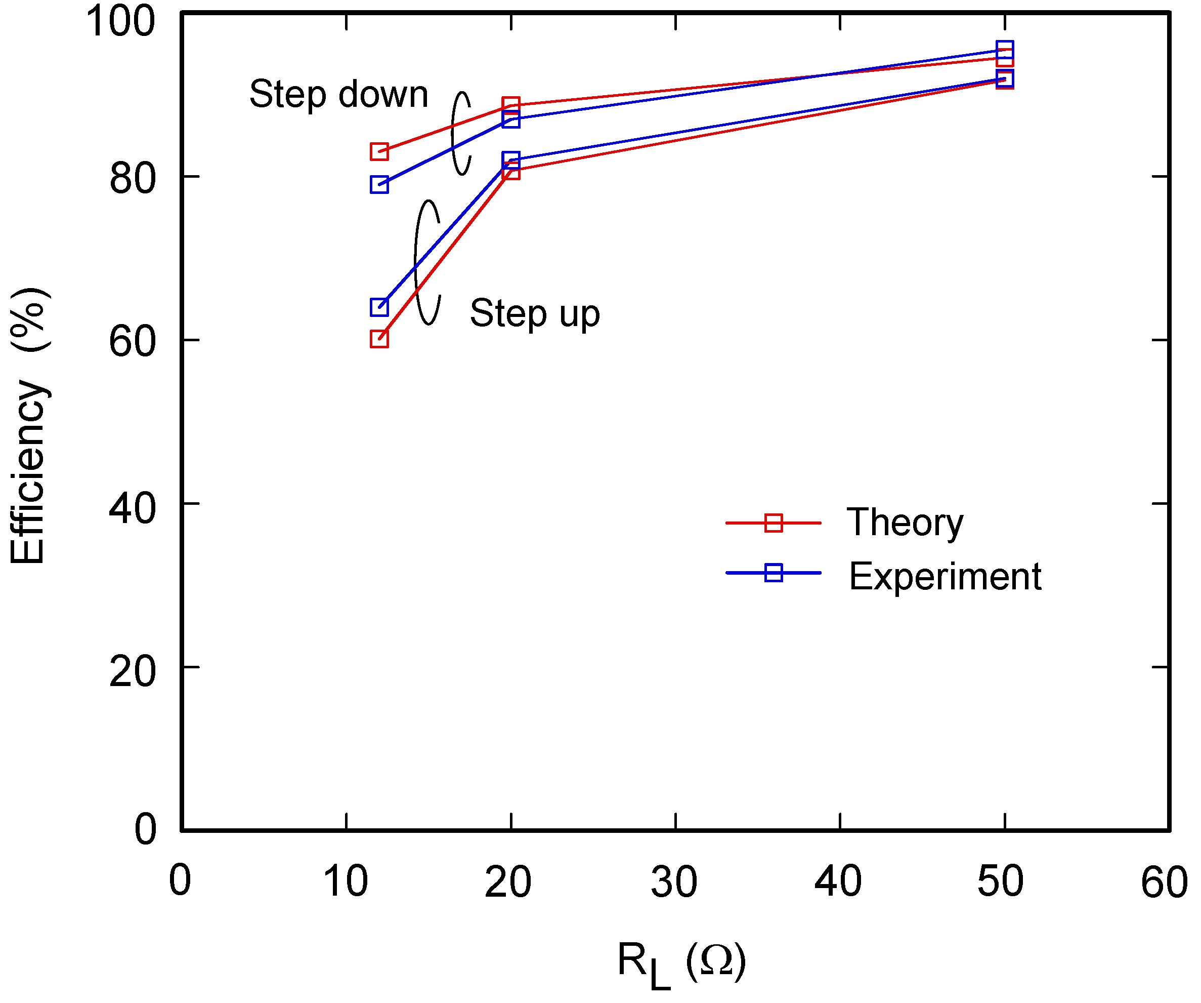
The experimental results are shown as blue lines in
Figure 8. When
decreased or, in other words, the power consumption increased, the efficiency decreased rapidly. The efficiency of the step-down circuit was larger than that of the step-up circuit when
was the same or, in other words, the output power was the same. This was the same characteristic as already discussed in
Figure 6. This result showed that discharging from series capacitors with a step-down circuit is superior to discharging from parallel capacitors with a step-up circuit.
Next, we considered the theoretical efficiency using the experimental physical parameters. In (5),
was assumed to be constant. However, in the step-down experiment, the average resistance of the pMOS and the diode
had to be considered. The ratio when the pMOS or the diode was turned on was
d or 1 −
d, respectively. Therefore,
was calculated as:
where
and
are the on-resistance in the pMOS transistor and the diode resistance, respectively. When
was 12, 20, and 50 Ω,
was 1.0, 0.6, and 0.24 A, respectively, due to an output voltage of 12 V. These values were calculated from
. The experimental
was well consistent with these values. The values of
and
were calculated with
from the equipment datasheets of 2SJ438 and 2GWJ42. Next, we considered the value of
d. When the output voltage was 12 V,
d could be estimated from the experiment. The values of
d at
= 12, 20, and 50 Ω were calculated as 0.80, 0.72, and 0.67, respectively. When
was comparatively large, such as 50 Ω, it was confirmed that the output voltage of 12 V was consistent with 0.67 × 18 V or, in other words,
. Using
d,
was calculated as 0.172, 0.297, and 0.827 Ω at
= 12, 20, and 50 Ω, respectively.
Similarly, in the step-up experiment, the average resistance of the nMOS and the diode
had to be considered. The ratio when the nMOS or the diode was turned on was 1 −
d or
d, respectively. Therefore,
was calculated as:
where
is the on-resistance in the nMOS transistor. When the output voltage was 12 V,
d was also derived from the experiment. The values of
d at
= 12, 20, and 50 Ω were calculated as 0.40, 0.54, and 0.66, respectively. When
was comparatively large, such as 50 Ω, it was confirmed that the output voltage of 12 V was consistent with 8 V/0.67 or, in other words,
. Using the measured power supply current, which was equal to
i,
and
were calculated from the equipment datasheet of 2SK2231 and 2GWJ42. Using these resistance values and
d,
was calculated as 0.172, 0.297, and 0.827 Ω at
= 12, 20, and 50 Ω, respectively. Inserting
and
into (5) and (6) instead of
, the theoretical efficiency could be calculated and is shown as the red lines in
Figure 8. These values were almost consistent with the experimental values.
4. Conclusions
In this paper, it is clarified using a theoretical method, circuit simulations, and experiments that discharging series capacitors with a step-down circuit is better than discharging parallel capacitors with a step-up circuit from the aspect of power efficiency.
This circuit can be applied in various situations. For example, an IoT (Internet of Things) society is being realized through innovative sensing technologies. A battery-less energy storage system using supercapacitors is useful for an IoT system. This is because supercapacitors have long service lives with a large number of charge and discharge cycles, and they are maintenance-free. The proposed circuit, which can efficiently charge energy into a supercapacitor and discharge energy from the supercapacitor, will be widely used in the future.
Other applications of supercapacitors are electric cars. They are already being used in electric vehicle hybrid systems and will be widely used in the future, not only for passenger cars and buses, but also for cranes, bulldozers, and excavators.
Capacitors are also useful in overhead wireless trains. Rapid charging systems with raised pantographs at stops will be widespread in the future.
A further important application is the storage of renewable energy, such as wind energy and solar power. Supercapacitors based on carbon elements have an advantage in that they are easier to recycle than battery cells. This means that the mass production of supercapacitors will not encounter major problems related to disposal. In a supercapacitor energy storage system, the highly efficient charge–discharge system based on series–parallel capacitor conversion proposed in this study would be extremely useful.
A future problem is the circuit design of series–parallel capacitor conversion. Whether transistors or mechanical relays should be used as switching devices should be considered in terms of cost, service life, and safety. The number of capacitors for series–parallel conversion was assumed to be two in this study, but it could also be four or more. The number of capacitors or capacitor modules is an issue that should be studied in the future from the perspectives of energy efficiency and circuit design.
By studying these issues, the proposed series–parallel capacitor conversion system is expected to make a significant contribution to solving problems in a wide range of energy fields, from the IoT to power sources for cars and trains and renewable energy storage.


