1. Introduction
With the rapid development of the electric vehicle industry, the demand for efficient, safe, and reliable battery management systems (BMSs) has significantly increased [
1,
2]. As the primary energy source for electric vehicles, lithium-ion batteries directly impact a vehicle’s range and safety [
3]. Therefore, the effectiveness of battery management systems not only determines the efficiency of vehicle operation but also has a profound impact on the sustainable development of the entire electric vehicle industry [
4]. However, traditional battery balancing methods, which typically rely on passive energy dissipation methods such as resistive discharge balancing, although relatively simple in structure, are inefficient and often result in significant energy waste. These methods fail to meet the modern electric vehicle’s demand for efficient energy management. As a result, developing new, efficient active balancing systems has become a critical research direction in the field of battery management [
5,
6,
7].
Currently, in the research of battery management systems, both academia and industry are focused on developing more efficient energy management methods. Some studies have introduced advanced technologies such as soft-switching techniques and resonant converters to enhance energy transfer efficiency and reduce energy losses during the battery balancing process [
8,
9]. These technologies have shown promising results in laboratory settings, effectively improving energy conversion efficiency and reducing internal resistance losses. However, in practical applications, these methods still face challenges such as complex wiring designs, high manufacturing costs, and insufficient system reliability, which limit their widespread adoption in large-scale battery management systems [
10].
In the industrial sector, the development of battery management technologies is also advancing continuously. Leading companies such as Panasonic (Osaka Prefecture, Kadoma City, Japan), and Samsung (Seoul, Republic of Korea) SDI are actively seeking innovative solutions for battery management systems. Panasonic and Samsung SDI have also made significant progress in enhancing battery balancing efficiency and system reliability, but technical bottlenecks remain, especially in large-scale applications, where balancing stability and efficiency in complex scenarios is still challenging [
11].
Compared to traditional passive balancing methods, active balancing technology has demonstrated significant advantages in battery management systems [
12,
13], particularly in handling large voltage discrepancies between battery cells. When substantial voltage differences occur within a battery module, active balancing technology can quickly adjust the voltage of individual cells, ensuring consistency and stability across the entire module. This approach is more efficient than traditional passive balancing as it reduces energy waste and significantly enhances the overall reliability and safety of the battery management system. As a result, active balancing technology has become a crucial component in modern battery management system design [
14].
In the context of the widespread application of lithium-ion batteries (LIBs) in electric vehicles (EVs) and grid-connected energy storage systems, the limitations of traditional wired battery management systems (BMSs) have become increasingly evident. As an emerging solution, wireless battery management systems (WBMSs) have garnered significant interest within the research community. Recent studies [
15,
16,
17] have not only laid an important theoretical foundation for the further development of WBMSs but have also revealed broad application prospects in areas such as electric vehicle battery health monitoring.
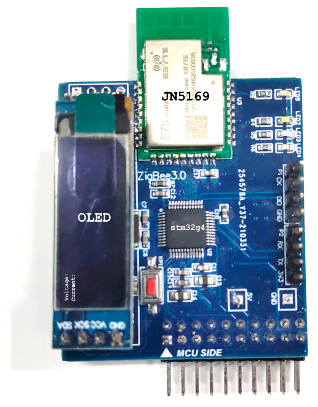
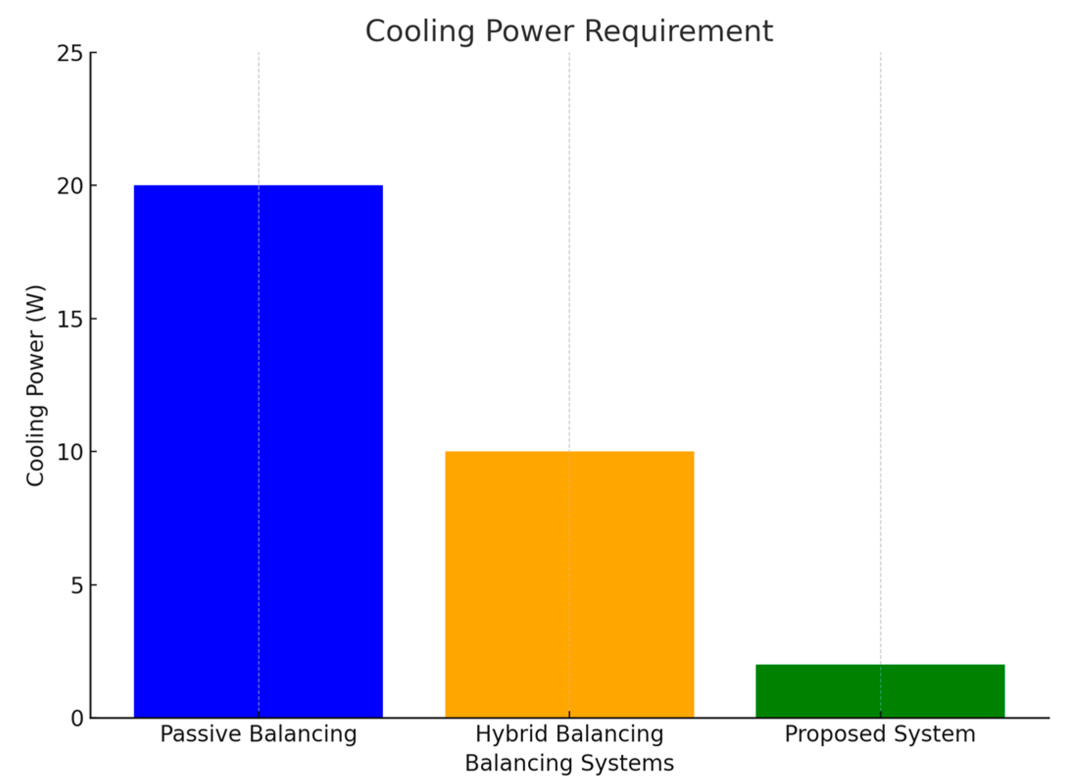
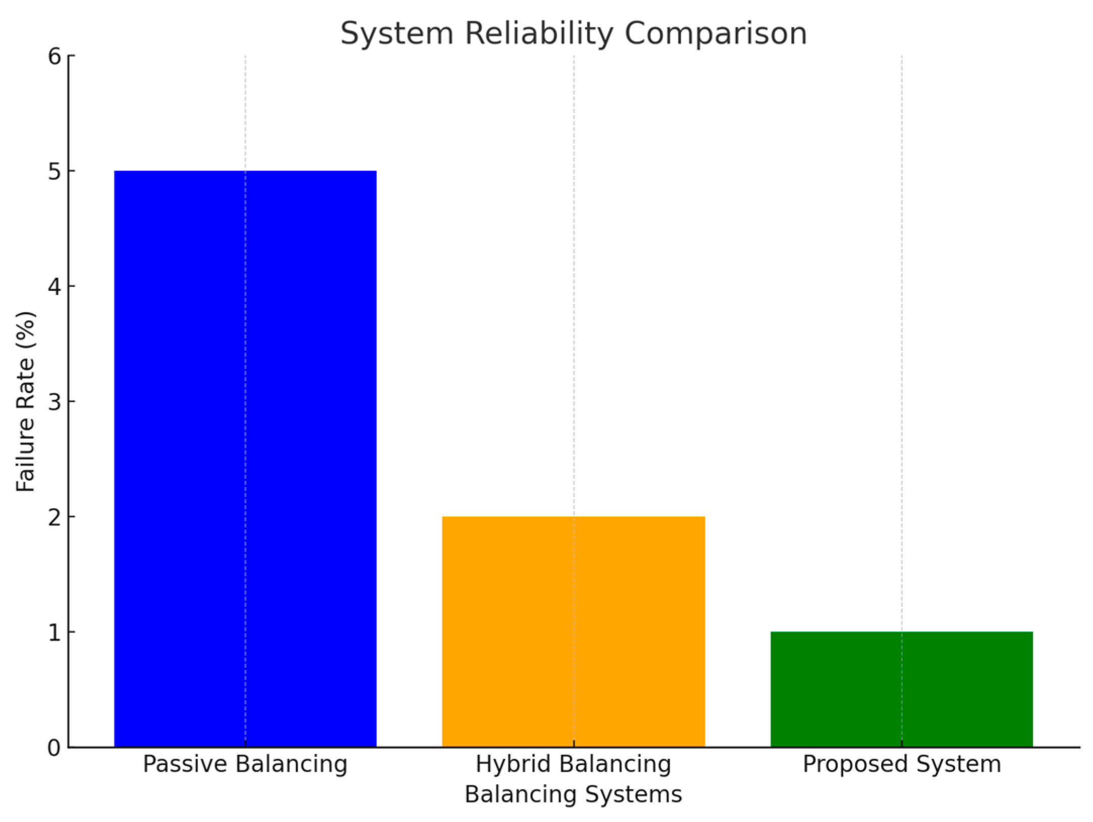
This paper proposes an innovative wireless hierarchical structure-based active balancing system for batteries, aimed at addressing the current challenges of low efficiency, high energy consumption, and thermal management in battery management systems by integrating wireless self-networking technology with advanced power electronics conversion techniques. This system simplifies the overall structure, reduces wiring complexity, and significantly lowers costs and weight, further enhancing the system’s flexibility and reliability.
The main innovations of this study are as follows:
Application of wireless self-networking technology: For the first time, wireless self-networking technology is applied to battery management systems, greatly simplifying the traditionally complex wiring designs. This technology not only reduces the system’s cost and weight but also enhances its scalability and adaptability, making it more flexible and reliable in various application scenarios.
Innovative hierarchical balancing method: A hierarchical balancing strategy is proposed, using a soft-switching LLC resonant converter for inter-group balancing and an active balancing control IC with a bidirectional buck–boost converter for intra-group balancing. This hierarchical design significantly improves the efficiency and speed of the balancing process while effectively addressing thermal management issues caused by energy dissipation, further enhancing the system’s overall stability and reliability.
In summary, the wireless hierarchical structure-based active balancing system proposed in this paper demonstrates significant technological advancements in the field of battery management, particularly in improving energy management efficiency, reducing thermal management burdens, and enhancing system flexibility and reliability. This innovative design provides a new technological solution for battery management systems in electric vehicles and other applications, with broad application prospects.
3. Hardware Design
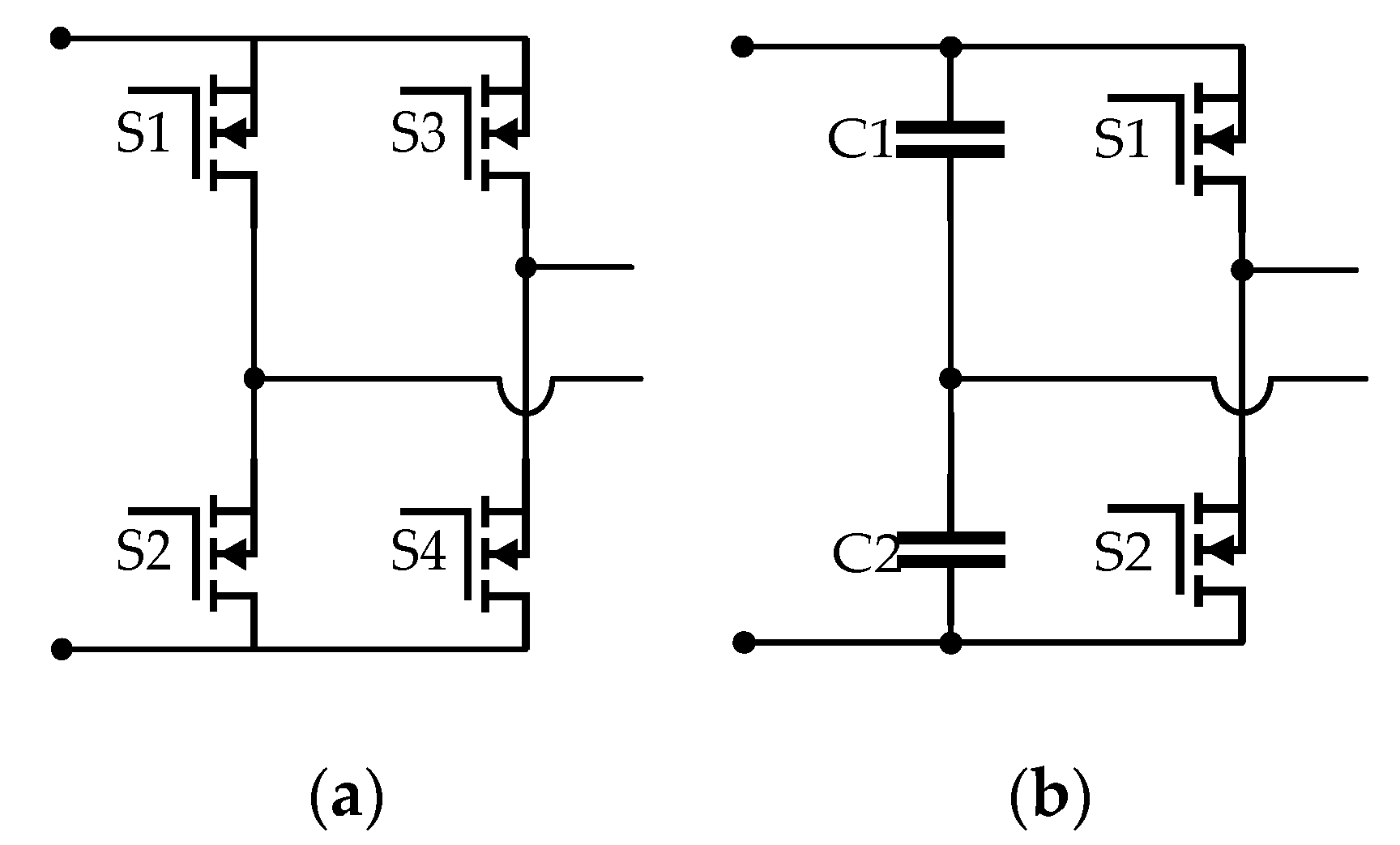
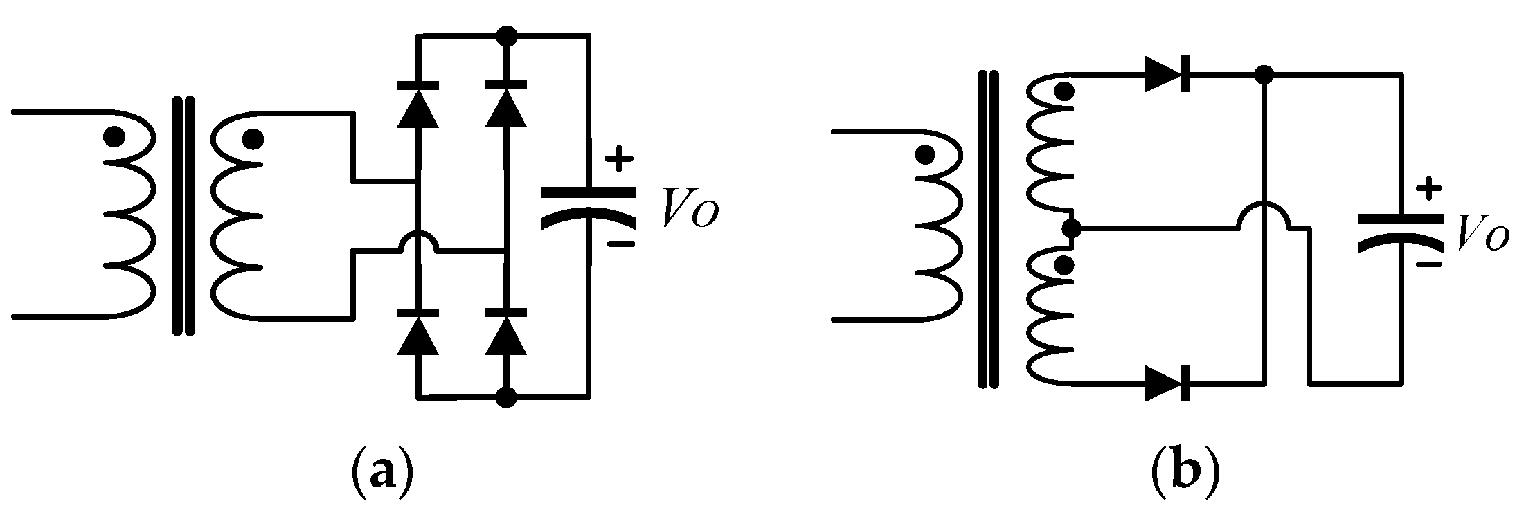
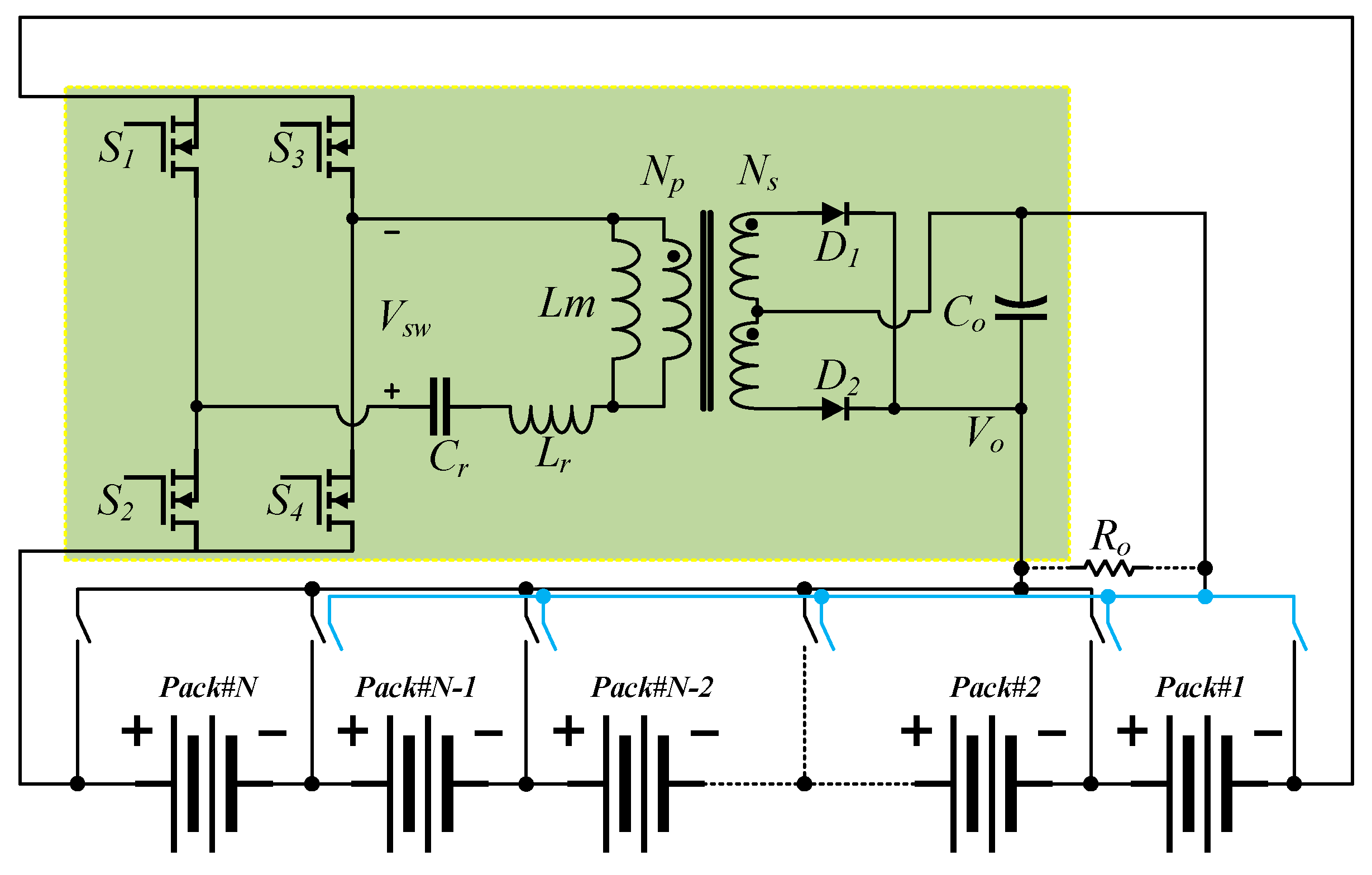
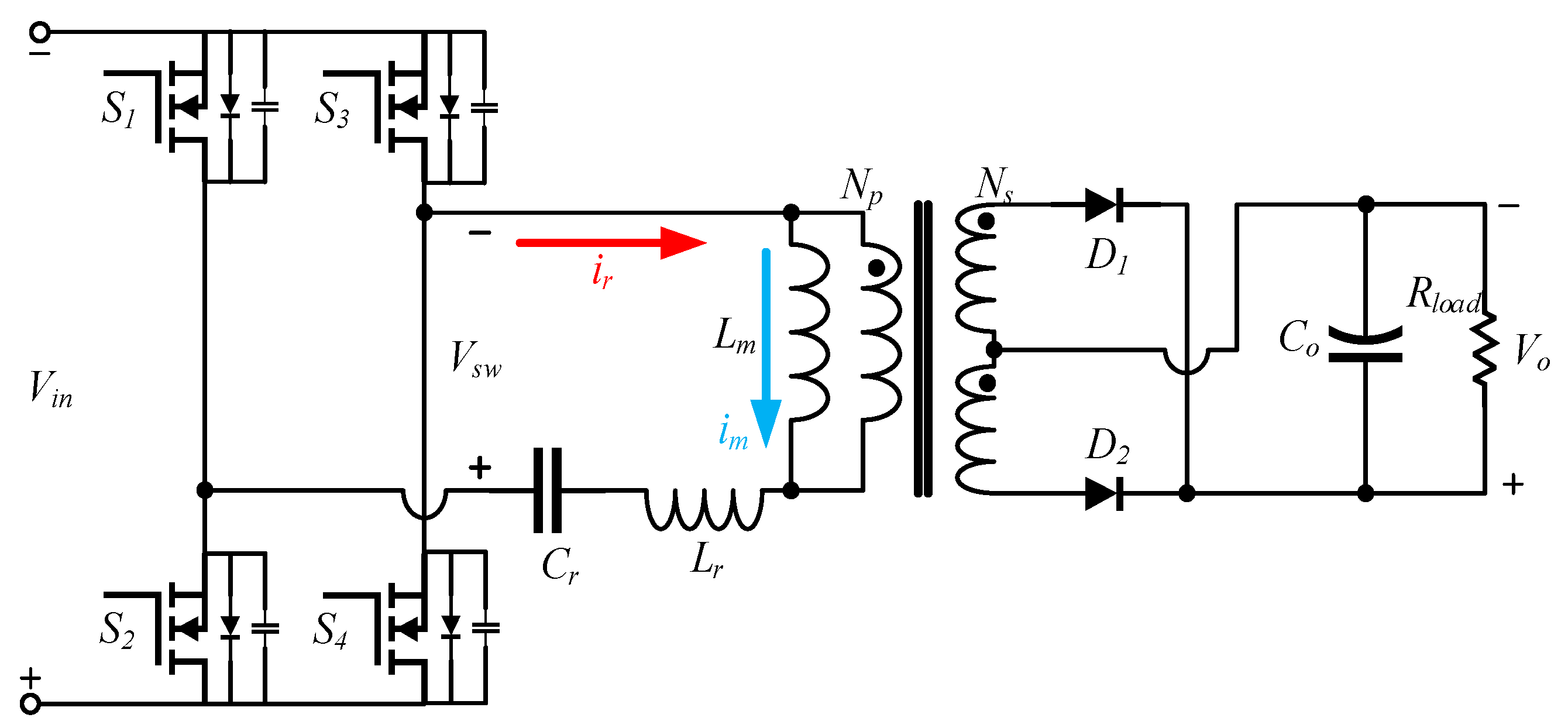
The chosen solution employs a full-bridge full-wave rectifier LLC converter as the balancing topology. A schematic diagram of this structure is shown in
Figure 4.
LLC converters offer several ideal characteristics compared to traditional hard-switching and other types of resonant converters. They feature high operating efficiency, low electromagnetic interference (EMI) emissions, and high power density, all of which are desirable traits for applications like onboard battery packs. As shown in
Figure 4, the yellow box highlights the main circuit of the LLC converter, with the primary excitation energy provided by the entire battery pack [
27]. The blue and black lines represent the double-switch structure used for battery gating. A high-speed switching bridge structure, consisting of power switches S1–S4, generates a square wave to excite the secondary resonant tank. The common control method for LLC converters is frequency modulation control. The resonant tank itself is designed with a resonant frequency, and under the excitation of square waves at different frequencies, the resonant tank outputs sinusoidal resonant currents that are in phase with the switching signals but with varying energy levels. The gain of the resonant tank, defined as the relationship between input and output voltage and current, measures this resonance. The output sinusoidal resonant current can be transferred through a transformer to the rectification structure, and eventually, after passing through output capacitors for smoothing and filtering, it achieves stable DC output. While the hardware structure of LLC converters is relatively simple, their parameter design involves some complexity. In the following sections, we delve into detailed discussions on the design of the resonant tank parameters and other components.
- (1)
LLC Operating States and Key Modes
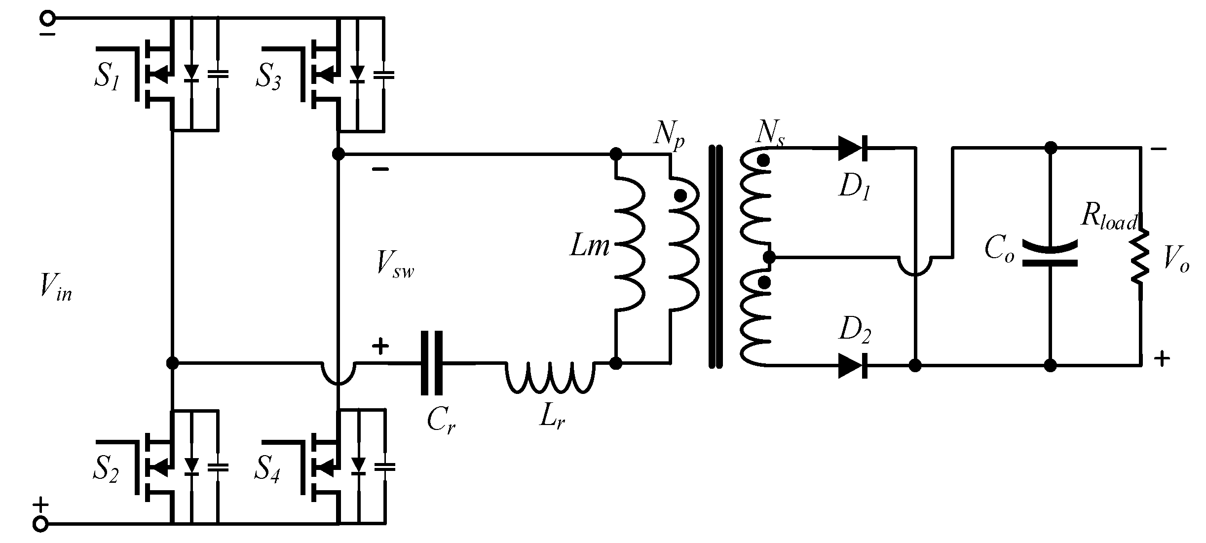
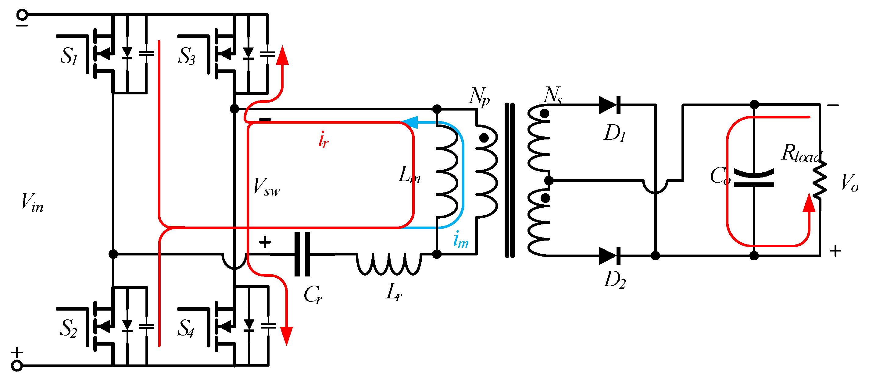
The LLC resonant converter’s resonant network has two resonance frequencies. The LLC operating states are defined based on the relationship between these two resonance frequencies and the excitation frequency of the switching bridge. In the project, a full-bridge LLC converter is utilized, and its individual structure is depicted in
Figure 5.
As shown in
Figure 5, the resonance frequency of the resonant network’s resonant capacitor Cr and resonant inductor
is generally denoted by
. Initially, when Cr and
resonate, energy is transferred from the primary side of the transformer to the secondary side. At this point, the primary-side coil is clamped due to the coupling effect of the transformer, so the primary-side magnetizing inductance
does not initially participate in resonance. Therefore, only series resonance occurs at this time. The expression for the resonance frequency
is as follows:
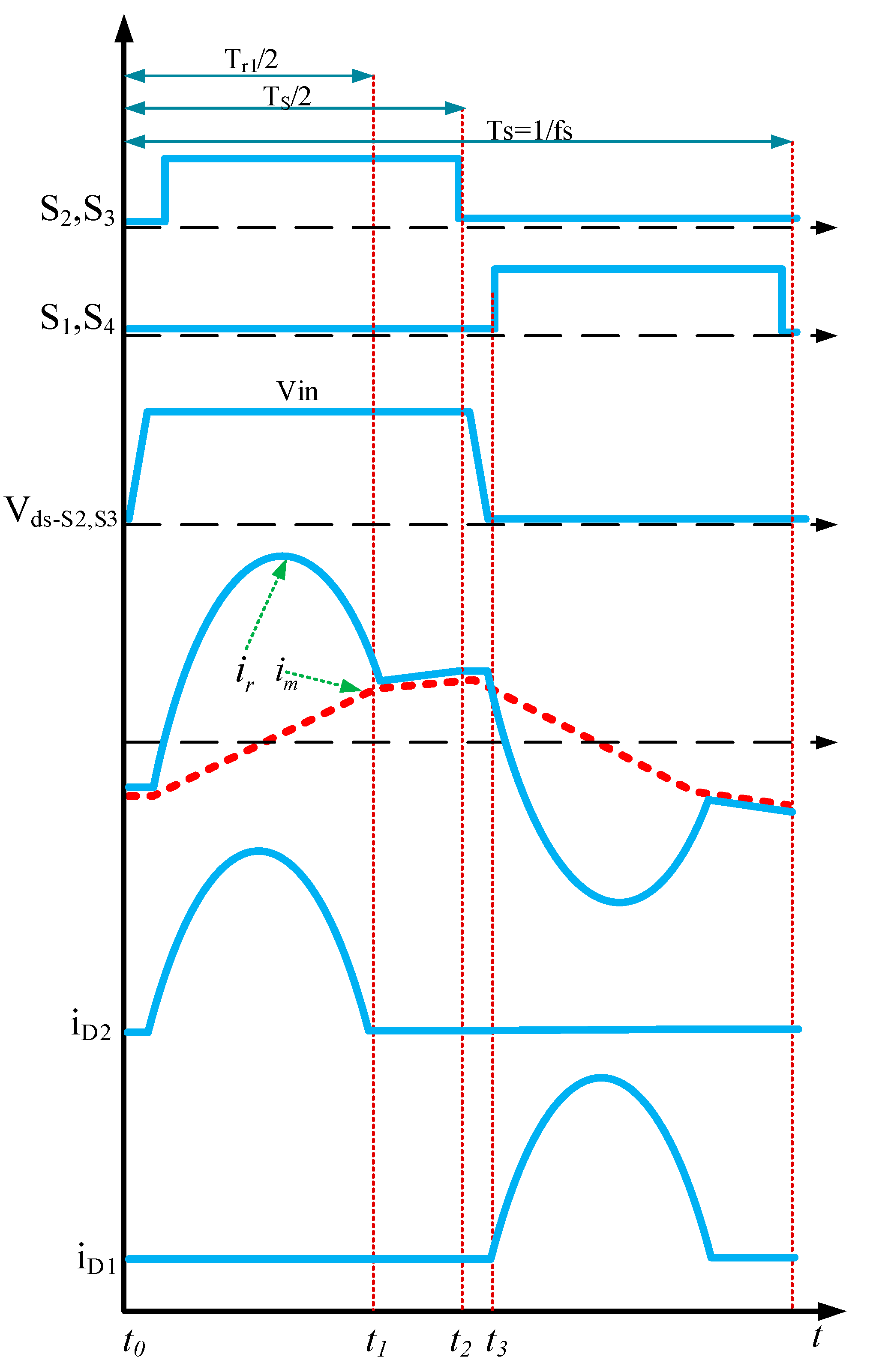
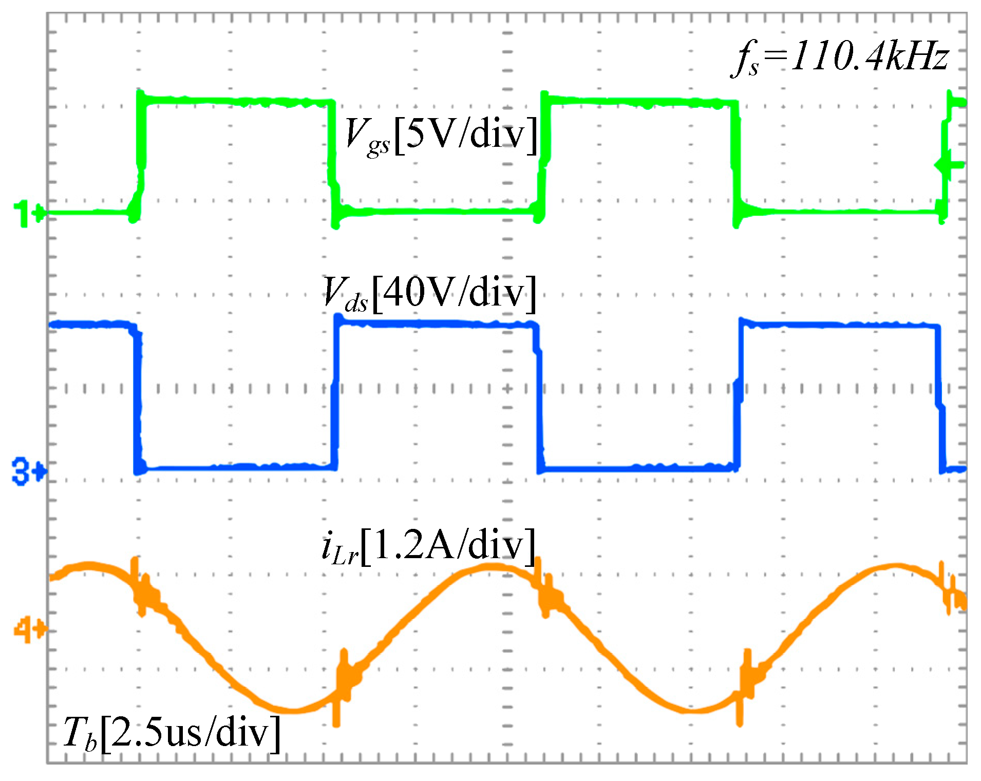
The resonant tank current over time is depicted in
Figure 6.
After the initial stage, the converter reaches a point where the resonant current
equals the magnetizing current
, as shown in
Figure 6. At this point, the magnetizing inductance
participates in resonance, resulting in series–parallel resonance. During this stage, energy is not transferred from the primary side to the secondary side. The expression for the resonance frequency
under these conditions is as follows:
By comparing the forms of Equations (1) and (2), it is evident that
must be smaller than
. With the determination of these two key resonance frequencies, we can now discuss the relative relationship between the switching frequency
and the resonance frequencies
and
, leading to three operating states of the LLC converter: under-resonance (
), quasi-resonance (
), and over-resonance (
). The corresponding resonant current waveforms for these three states are illustrated in
Figure 7a–c, respectively.
Among the three operating states mentioned above, the under-resonance state encompasses all resonance states and exhibits soft-switching characteristics. This state is the main focus of our analysis, focusing on several operating modes.
The timing waveforms are depicted in
Figure 8.
The current state of mode 1 (
) is illustrated in
Figure 9. It is assumed that all resonance involving the output capacitors of the switching transistors is ignored, and all device characteristics are ideal.
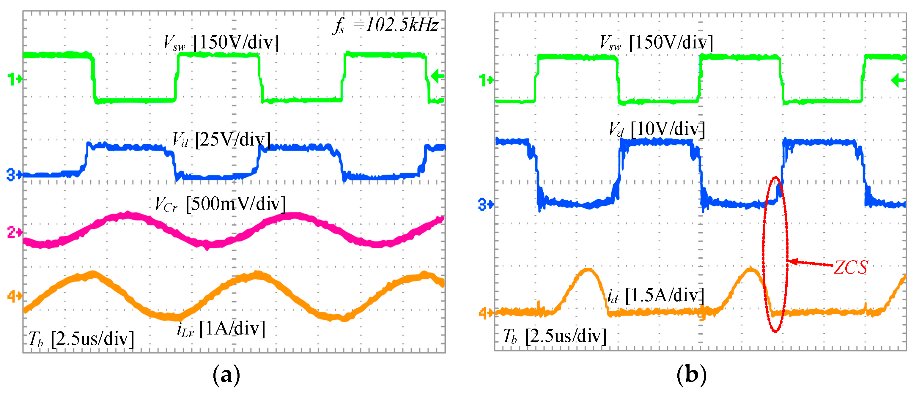
At time , the switching transistors and , and the secondary-side diode are conducting. At this point, only series resonance occurs in the network. The resonant current is a sinusoidal resonant current, while the magnetizing current linearly increases. At time , the two currents are equal, at which point the current through the secondary-side diode drops to zero, and then, reverse voltage is applied to achieve zero-current switching (ZCS). Subsequently, mode 2 is entered.
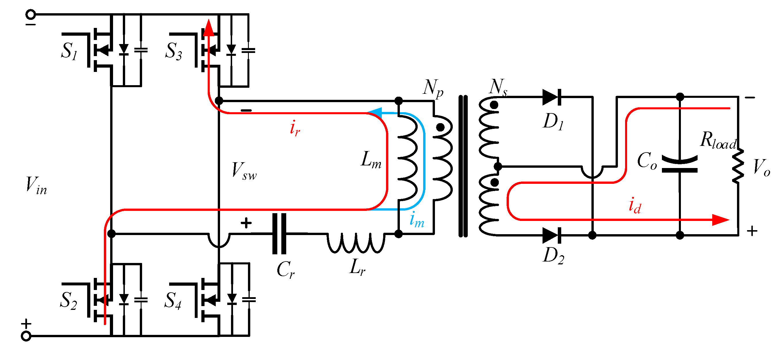
The current distribution during mode 2 (
) is depicted in
Figure 10.
At time , the resonant current equals the magnetizing current . At this moment, no energy is transferred from the primary side to the secondary side, so the two arms of the rectifier bridge are in reverse-bias cutoff state. At this time, the primary-side coil participates in resonance, which is equivalent to three components undergoing series–parallel resonance. The resonance frequency at this time is , as mentioned earlier. Since the inductance of is greater than that of , the corresponding series–parallel resonance frequency is lower. This is manifested in the waveform as a decrease in slope. At time , and are turned off, entering mode 3.
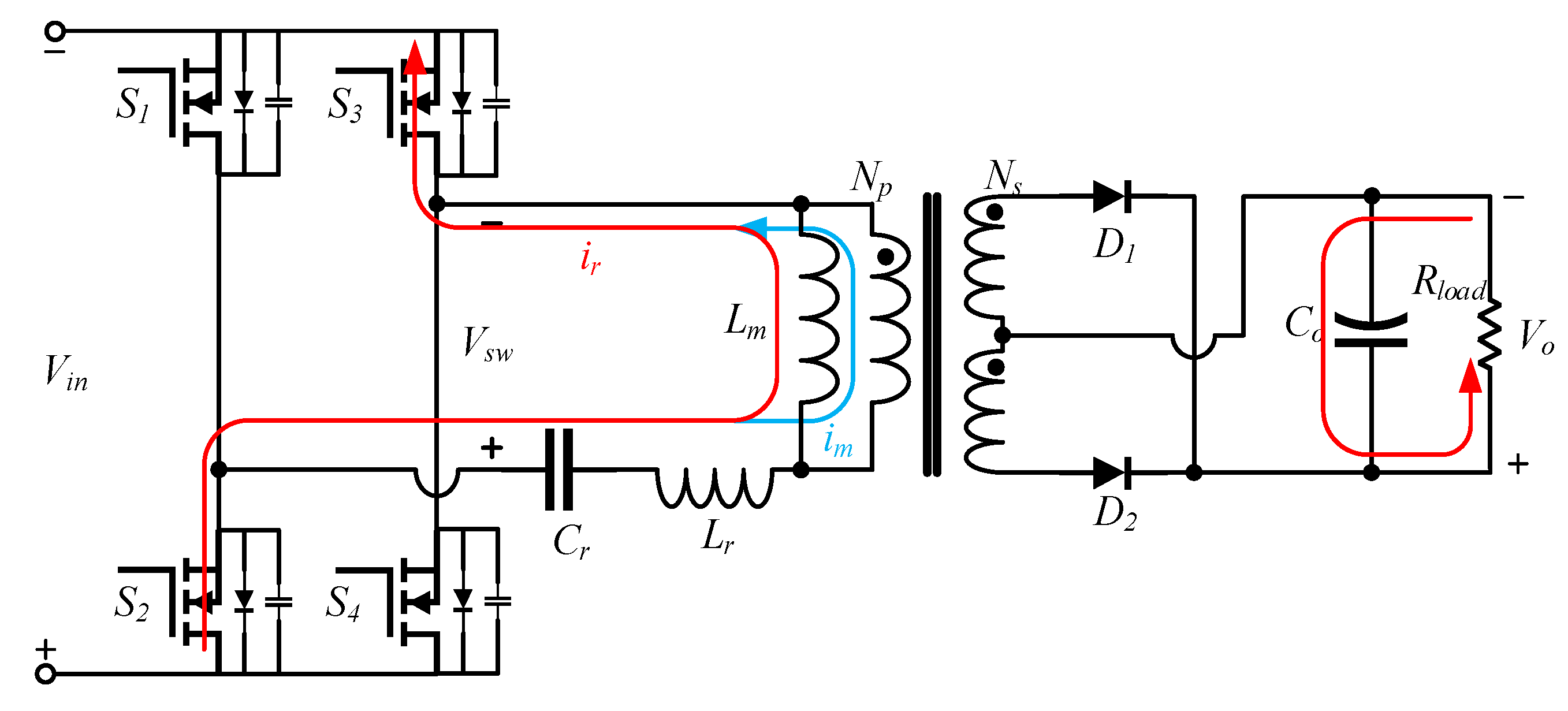
The current distribution during mode 3 (
) is depicted in
Figure 11.
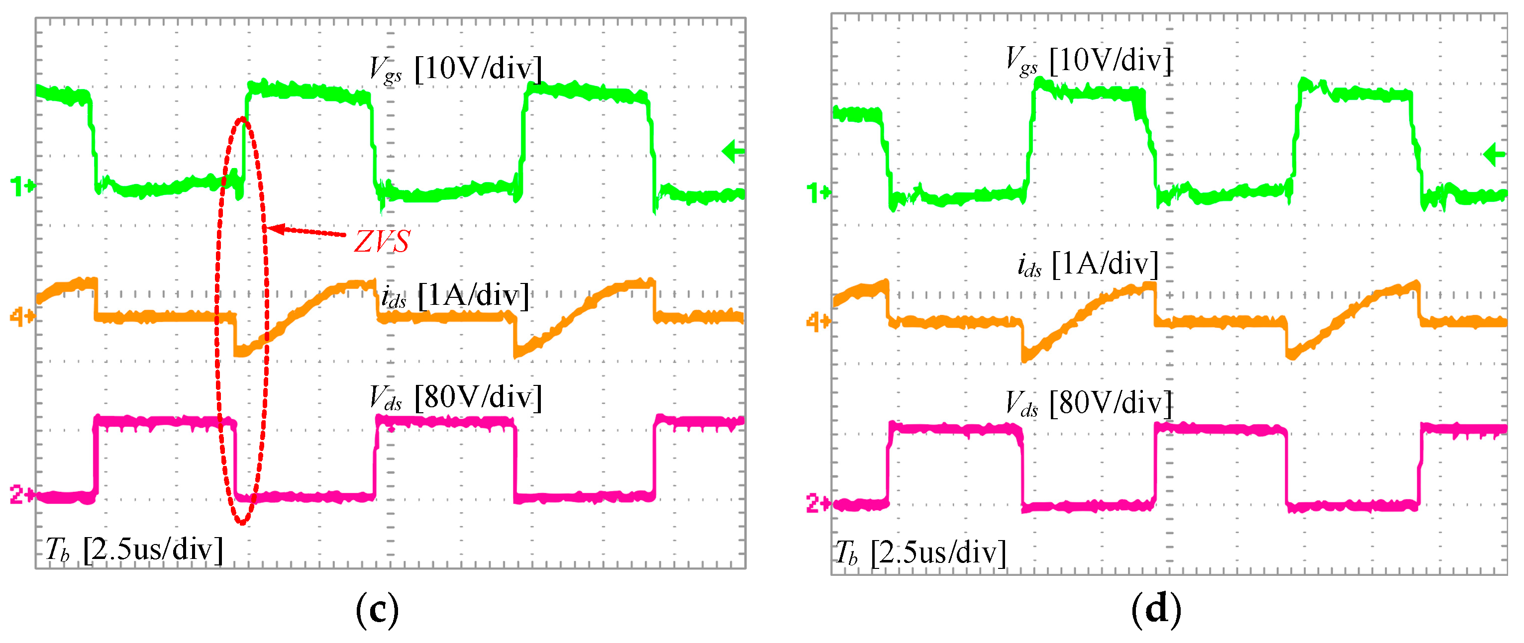
This is one of the most critical modes involving soft switching. At time
, all switches enter the off state. At this moment, the resonant current does not experience any sudden changes. It charges the output capacitors of
and
according to the path shown in the figure, while discharging the output capacitors
and
. The dead time should be greater than the time it takes for the output capacitors to discharge to zero. Discharging to zero provides the basic condition for zero-voltage switching (ZVS) during the next switch-on. ZVS is the second soft-switching state that LLC converters possess, following ZCS. This period of time is of significant engineering reference value for embedded chips. By applying Kirchhoff’s current law (KCL) and solving differential equations, we can derive an approximate expression for the minimum time required for the output capacitors to discharge to zero, as shown in Equation (3).
In the equation, represents the output capacitance of the switch. The dead time generally lasts for a short duration. Therefore, the current remains approximately constant during this period. Thus, the current at time is taken as the value of the current during the entire dead time for calculation purposes. Subsequently, at time , the converter enters the zero-voltage switching (ZVS) stage and transitions to the subsequent mode. The analysis in this stage is similar to the above and will not be reiterated here.
- (2)
LLC Parameter Calculation
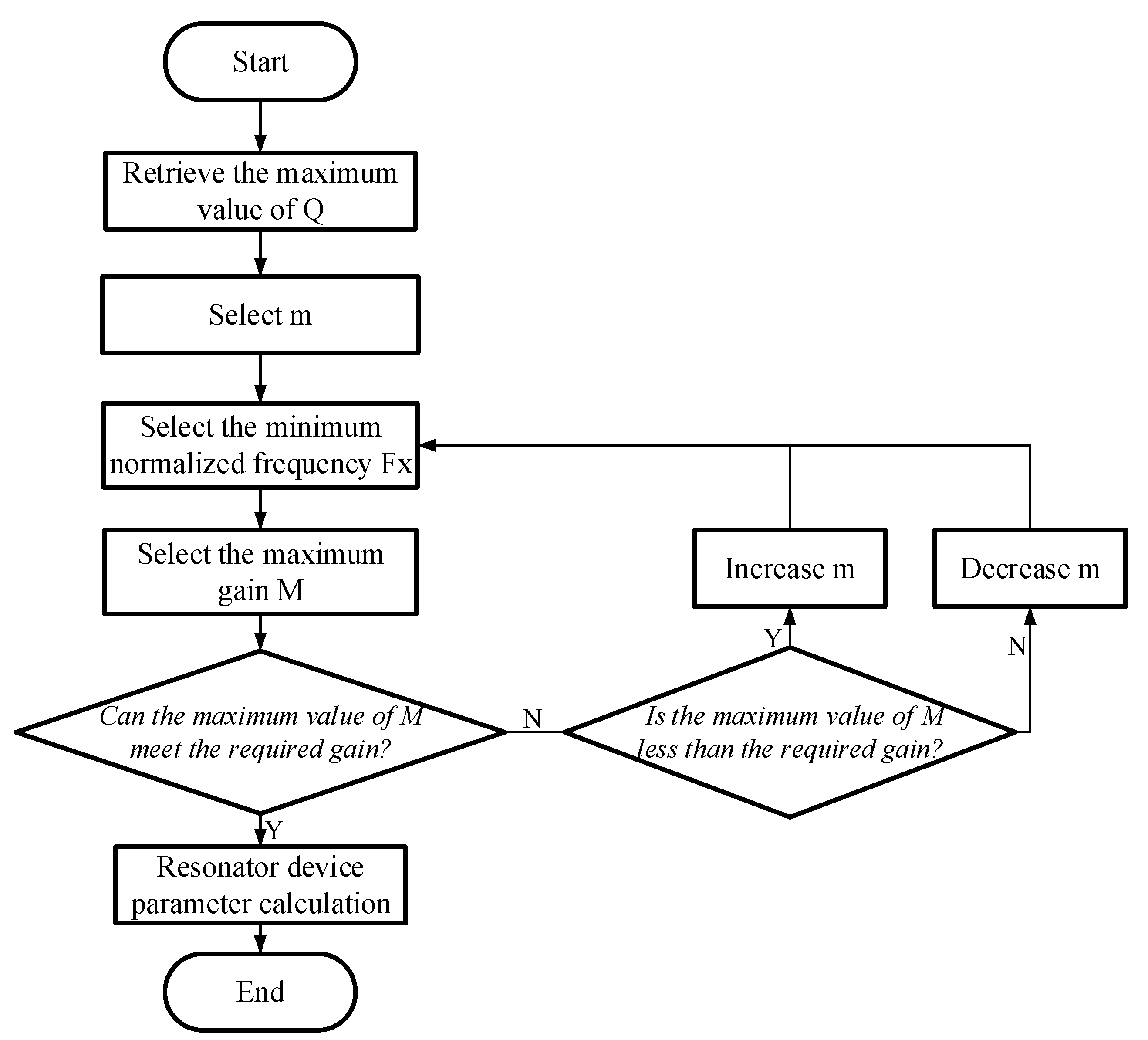
LLC parameter calculation relies on the derived expressions mentioned earlier. The main design process flowchart is depicted in
Figure 12. The design process starts with the selection of Q and m values, which are used to determine the specifications of the resonant circuit. Subsequently, iterative calculations are performed to ensure that the maximum DC gain meets the required specifications. At each step, various loss factors in the actual design are also considered, and parameters are adjusted to optimize performance. Finally, all key parameters are verified to ensure the effectiveness and reliability of the design.
The basic parameters of the battery pack are shown in
Table 3.
The input voltage of the LLC converter is equal to the total voltage of the battery pack. Its nominal value is 74 V, with the maximum value calculated using the fully charged voltage of 4.2 V, resulting in 84 V. The minimum value is calculated using the undervoltage of individual cells at 3.4 V, resulting in 68 V. Each group consists of four 18,650 lithium-ion cells. Based on calculation with the individual cell voltages mentioned earlier, the maximum value is 16.8 V and the minimum value is 13.6 V. The maximum charging current of the battery pack is taken as 2 C, which is 5.2 A.
The input voltage range of the LLC converter is taken as 70–94 V, and the output voltage range is 14–16.5 V. The output voltage ripple requirement is not high and is set at a maximum of 1 V. The maximum output current is 5 A, resulting in a maximum output power of approximately 83 W. The series resonant frequency of the converter is set at 100 kHz.
Firstly, we need to determine the turns ratio
N of the transformer. The turns ratio of the transformer must satisfy the condition that the minimum output voltage can be obtained at the maximum input voltage. Calculating according to Equation (4), we obtain
N to be approximately 6.7. Considering the voltage drop caused by the rectifier bridge diodes, the voltage drop in the switching transistor, and other parasitic parameters, we take
N as 6 in the actual design to compensate for these losses.
Then, the DC gain range needs to be determined, that is, to solve for
and
, which are calculated according to the formulas shown in (5).
Substituting into Equation (5), we finally obtain and .
Next, the equivalent load impedance
is calculated using the transformed expression derived earlier, as shown in Equation (6).
When Vo is at its minimum value, the minimum equivalent secondary-side resistance is calculated to be . When is at its maximum value, the maximum equivalent secondary-side resistance is calculated to be .
Taking
and
m = 6.3, the values are not directly calculated here. Instead, a set of
Q and
m values is first chosen according to the method shown in
Figure 12. Then, after calculating all the parameters, the maximum DC gain corresponding to
is verified to determine whether the selected values should be used.
Next, we first solve for the minimum normalized resonant frequency value
. According to the curves corresponding to different
Q values shown in
Figure 12, when
Q and
m are fixed, there is a unique curve corresponding to them. When the curve is at its gain peak, the corresponding normalized resonant frequency is
. Therefore,
can be calculated according to the following equation:
is approximately 0.667. At this point, we can also calculate the boundary switching frequency of the converter’s capacitive–inductive working region, .
Next, we verify whether the selected Q and m values can meet the gain requirements of the converter. Directly substituting , m, and the obtained into the DC gain expression, we find that the DC gain at this point is approximately 2.34, which is greater than . Therefore, the selected Q and m values meet the design requirements without the need for further iteration.
Next, we calculate the values of the resonant components by solving the system of equations below:
We obtain , , and .
The LLC power supply input side is structured as a full bridge. The maximum withstand voltage at the primary side is around 90 V. Considering the dynamic situation of the full bridge where two closed bridge arms simultaneously withstand the voltage of the battery pack, the voltage tolerance of each switch needs to be greater than 90 V. Additionally, we need to calculate the effective value of the current flowing through the switch devices. Assuming a converter efficiency of 95%, the calculation expression is as follows:
The calculated effective current is approximately 1.2 A. Based on the above calculation results, the UMW15N10 N-channel MOSFET from UMW company (New Taipei City, Taiwan, China) is selected. Its single-device breakdown voltage is 100 V, which is approximately twice the safety threshold when both bridge arms withstand the voltage. Its on-state resistance is approximately 60 , and its maximum continuous drain current capability is 10 A.
For the resonant inductor, a discrete design is adopted instead of using transformer leakage inductance. The inductance is chosen as an integer value of 8
based on the theoretical value calculated earlier. The PQ2020 magnetic core is selected. The peak resonant current obtained earlier is approximately 1.7 A. The total area and number of turns of the coil are calculated according to the following formula. In actual wires, the effective cross-sectional area decreases due to the skin effect when passing high-frequency currents. This reduction is generally measured using the skin depth
, as expressed in Equation (10).
The maximum switching frequency is calculated under the condition of maximum output voltage at no load and maximum input voltage, resulting in approximately 115 kHz. It is appropriately rounded up to 125 kHz for calculation. Here, represents the electrical conductivity of copper, represents the relative permeability, and represents the vacuum permeability. The calculated skin depth is approximately 0.443 mm. The wire diameter should be less than half of the skin depth, so a wire diameter of 0.2 mm is selected.
The formula for the number of turns is expressed as Equation (11).
The number of turns of the inductor coil wire is approximately 120, calculated using the formula, where d is the wire diameter (0.2 mm); J is the current density coefficient, typically taken as the empirical value of 450 A/cm2; and I is the peak current (1.7 A).
Transformer design generally employs the AP method, which considers factors such as operating frequency, magnetic flux density, and core losses. Since an external discrete resonant inductor is used, minimizing magnetic leakage and flux leakage in the transformer core is important. The PQ-type magnetic core is selected. The AP factor is defined as the product of the core cross-sectional area
and the window area
, calculated using the formula shown in Equation (12), with units in
.
In Equation (12), k represents the window utilization factor, typically ranging from 0.15 to 0.4. Here, we take k = 0.3 for calculation purposes. denotes the rate of change of magnetic flux density, which depends on the magnetic core material and structural dimensions. A value of 300 mT is commonly chosen based on engineering experience. The calculated AP value is approximately 19.4 . Selecting the PQ3230 magnetic core meets the requirements.
After selecting the magnetic core, the number of turns for the secondary coil is calculated according to Faraday’s law of electromagnetic induction, as shown in Equation (13).
The magnetic core has an value of 80 mm2. Assuming the lowest switching frequency, the calculated number of turns for the secondary coil is approximately 5. Using the turns ratio, the number of turns for the primary coil is determined to be 30 turns. The skin depth can be calculated based on the results of the resonant inductor calculated earlier. Using a wire diameter of 0.2 mm, the number of strands is calculated according to Equation (11), resulting in approximately 120 strands for the primary side and about 500 strands for the secondary side.

