1. Introduction
The low-voltage current transformer, as an important device for power measurement, is an important part of the fair trading of power and billing between power supply enterprises and power customers. Whether the low-voltage current transformer is objective and accurate concerns the interests of the majority of users and power supply enterprises, and its accurate measurement is of paramount importance [
1]. As early as the 1960s, domestic and foreign current transformers for 0.1 to 10 levels were used to carry out calibration work. After the 1970s, the measurement level of current transformer calibrators [
2,
3,
4] was greatly improved and the related calibration techniques became more and more mature. In the 21st century, the current transformer calibration technology has gradually shown a trend of intelligence [
5,
6,
7,
8,
9,
10,
11,
12]. Traditional calibration requires manual inspection, and in order to reduce manpower and improve efficiency, a system was designed for the automatic inspection of finished CT products, which can be used for the appearance inspection of inductors, an insulation resistance test, a frequency withstand voltage test, a secondary winding turn-to-turn insulation test, a magnetic saturation margin test and error measurement [
13,
14,
15,
16,
17]. In an effort to increase the range and improve accuracy, some researchers have also created online calibration systems. These systems employ a variety of techniques, including bang-bang control and magnetic potential compensation, but they are all challenging to fully calibrate [
18,
19,
20,
21]. Reference [
22] also designed a wide-band standard current transformer as a reference source for evaluating the current error and phase shift of inductive CTs at distorted current harmonics. Reference [
23] gives a wide frequency model for high-frequency transformers. In summary, although there have been a number of studies on the calibration of current transformers in the literature, a complete methodology for the full-scale calibration of current transformers under energized conditions is still in limbo. In this paper, a complete charged calibration scheme is proposed based on the above studies.
Although a lot of research has been carried out on electronic current transformers, electromagnetic transformers are very commonly used in power grids, and research into them is still of great significance. For the calibration of low-voltage current transformers, this paper proposes a full-range online calibration method and designs a calibration device.
Currently, particle swarm optimization (PSO) and genetic algorithm (GA) are the most widely used global optimization algorithms. Compared with genetic algorithms, particle swarm algorithms are more practical in engineering calculations because of their simple parameter settings and fast convergence speeds. PSO is a stochastic evolutionary algorithm that can find the global optimum within a complex search interval. When there is more than one objective function, a multi-objective particle swarm optimization (MOPSO) algorithm can be used for finding the optimum.
In production practice, economic efficiency is often improved by optimizing the production and operation scheme of the equipment. Reference [
24] applied the multi-objective particle swarm algorithm to the primary frequency regulation of hydroelectric units to achieve the primary frequency regulation parameter optimization, to achieve the purpose of optimizing the rise time and regulation time by adjusting the primary frequency regulation PID control parameters of the governor. Reference [
25] applied the multi-objective particle swarm algorithm to the rational allocation of an energy storage system to obtain the optimal location information, capacity size and corresponding operation strategy of ESS in an active distribution network. In [
26], a multi-objective particle swarm algorithm was applied to the parameterization of a first-order self-resistant controller, and the obtained parameters enabled the LCL grid-connected system to obtain better tracking, disturbance immunity, and quality of the incoming current. Reference [
27] applied the multi-objective particle swarm algorithm to the optimization problem of a combined cooling, heating and power (CCHP) system containing wind turbines, photovoltaics and energy storage, which improved the energy utilization of the CCHP system and reduced the operating costs and pollutant emissions. Reference [
28] applied multi-objective particle swarm algorithms to home smart electricity use to achieve the purpose of reducing electricity costs and improving the comfort of electricity use.
The booster, which is essentially a transformer, is one of the crucial components of the calibrating equipment. Reference [
23] gives a wide frequency model for high-frequency transformers, involving parameters with specific physical meanings, and thus the model has a wider range of adaptability and better inference ability. Meanwhile, the model uses typical high-dimensional complex function.
In this paper, a comprehensive and innovative approach is presented to address the challenges of calibrating low-voltage current transformers under energized conditions. The calibration device is first designed in detail, then combined with the PSO algorithm used to optimize the transfer function of the harmonic elimination loop to achieve a higher calibration standard, and finally an experimental circuit is built with the fabricated prototype of the device for the verification of the offset effect, which proves the validity of the proposed method.
2. Electrically Charged Calibration Program and Design of the Calibration Device
Since the full-scale calibration of low-voltage current transformers for metering under energized conditions is different from laboratory calibration, the primary side current of the low-voltage current transformer will have multiple sources of interference in addition to the industrial frequency and harmonic currents. Therefore, it is necessary to introduce the corresponding signal in the system design to eliminate the current generated by the interference sources. In this paper, the principle of active noise reduction is used to offset harmonics and noise from the primary current.
In full scale calibration, the rated frequency current to be output by the programmable power supply unit will need to vary according to the primary rated frequency current. This method is referred to as the rated frequency method.
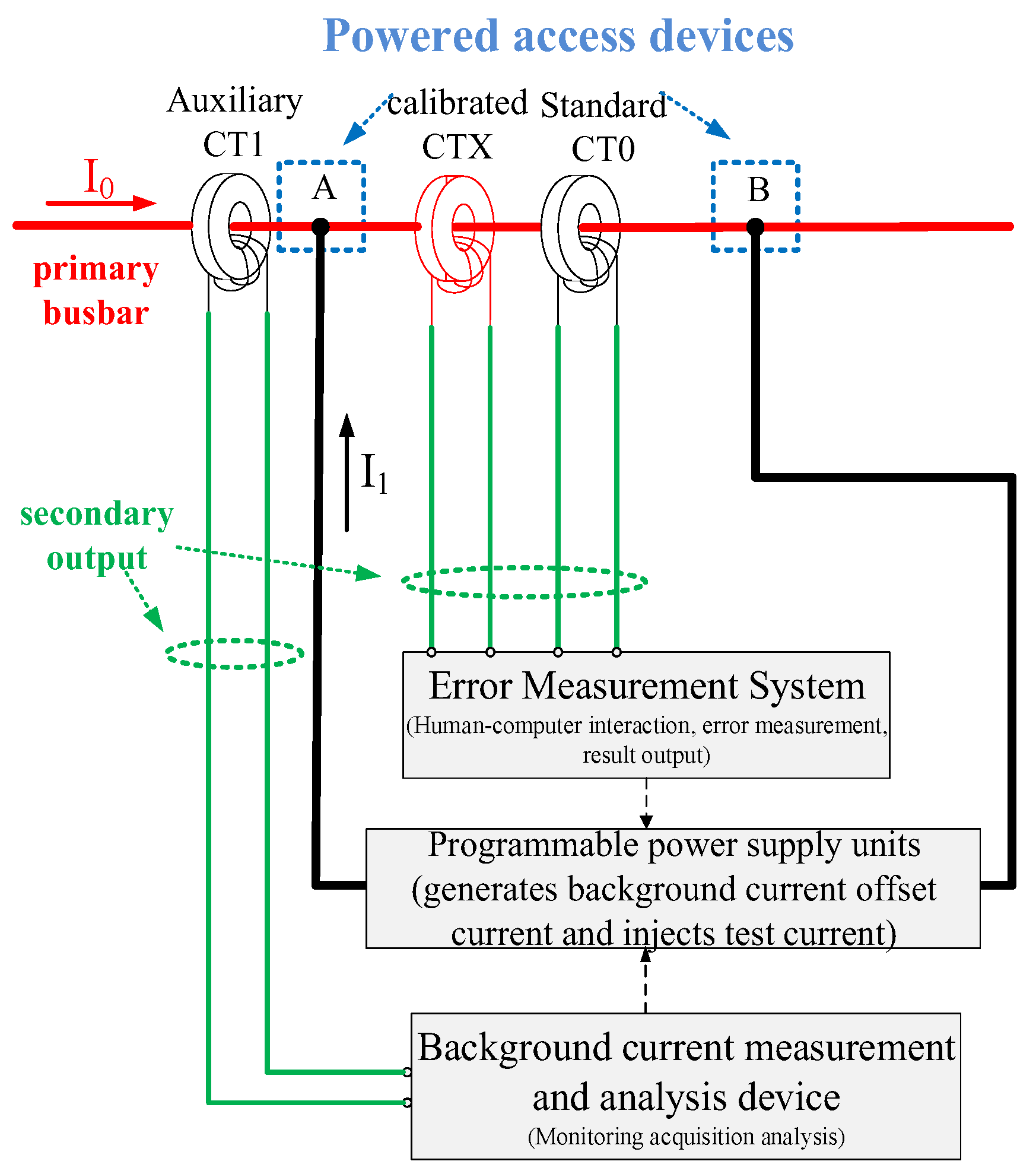
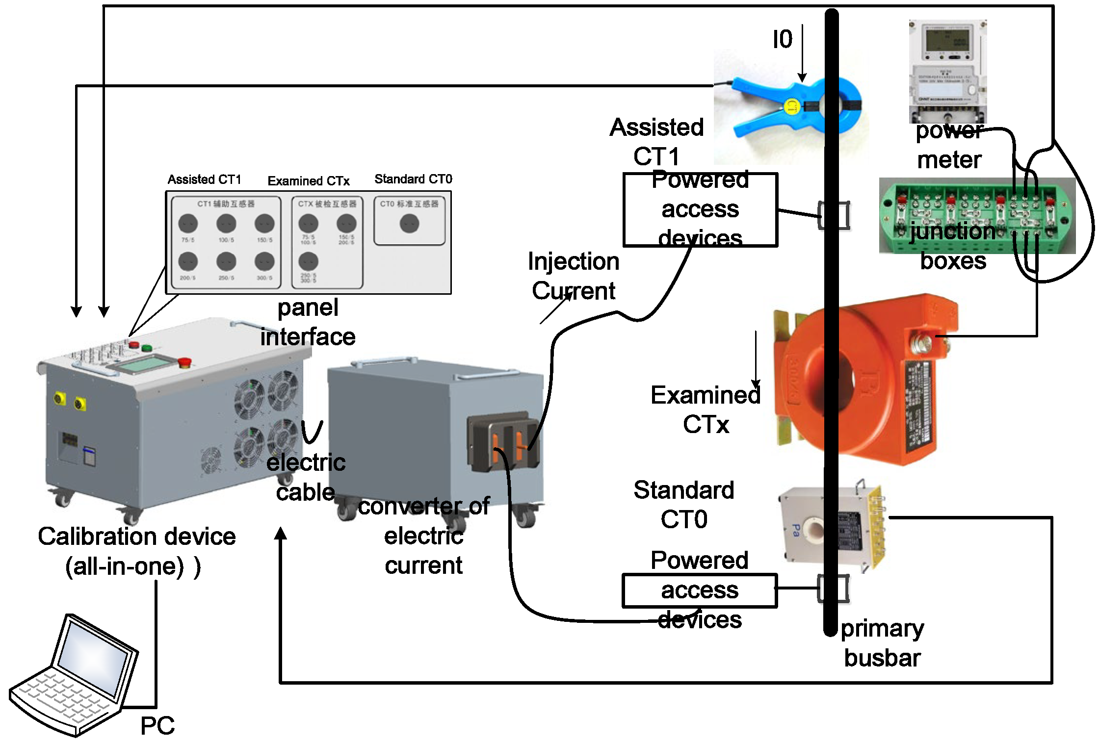
Industrial frequency method calibration wiring was as shown in
Figure 1, mainly using standard CT0, auxiliary CT1, program-controlled power supply, error measurement device, and charged access and other devices.
As indicated in
Figure 1, the CTX is in the charged conditions to carry out full-range calibration of the examined low-voltage current transformer. The primary busbar through the center of the CTX is connected to the customer’s load, and the secondary signal circuit of the CTX is schooled into secondary loads such as energy meters. The customer side of the main current has an amplitude ranging from tens to thousands of amperes, and the primary side of the main supply line voltage is either 220 V or 380 V low voltage. The primary current is the current output of the programmable power supply device, and is connected to the current output of the CTX through the wires. In order to realize the full-range calibration of low-voltage current transformers under charged conditions, the wiring process in the figure is as follows: the programmable power supply unit’s current output is connected to the conductor through the measured CTX, in which the standard current transformer CT0 passes through the busbar; CT1 is connected to the secondary circuit of the measured CTX; and the secondary circuits of CT1 and the standard CT0 are connected to the error measurement device together.
The working steps during calibration are as follows: The first step involves relying on the background current analyzing device with adaptive tracking sampling technology; the primary side current is first sampled by CT1, after the background current has been analyzed and extracted, and then the amplitude and phase of the collected signal are adjusted to be proportional to the amplitude of the primary side current and opposite to the phase by the phase control unit. The phase shifting and amplitude control of the sampled signal of the background current are then completed. For the second step, the program-controlled power supply amplifies the current to the same size as the background current, and outputs the background-inverted current into the primary side loop to realize the offset function of the background current on the primary side; according to the requirements of the full-scale calibration, the program-controlled power supply also needs to output the corresponding frequency current, and adjusts the output current according to the size of the primary current frequency current, which is synthesized into current I1 together with the background offset current and applied to the CTX being calibrated. This current and the background offset current are jointly applied to the calibrated CTX.
For the third step, using the error measurement device for error measurement, the standard CT0 secondary signal, the secondary signal of the calibrated CTX at the same time into the frequency error measurement device, the device, the standard CT0 secondary signal, and the secondary signal of the calibrated CTX extraction, as well as comparison and calculation, were all used to obtain the measured CTX ratio difference and angular difference and other calibration data to achieve the calibration of the current transformer.
According to JJG313-2010 and other standards, the harmonic content should be less than 5% at the time of calibration, while the calibration index proposed in this paper is that the primary current amplitude of 1%~120% of the full range of the accuracy level should reach the 0.05 S level. In view of the above problems and indexes, this paper adopts the active regulation technique of the primary current, which firstly extracts the harmonics of the primary current, then injects the opposite harmonic currents to offset the harmonics by using a penetrating wire, and finally carries out charged calibration. Since the harmonics may contain high harmonics, the difficulty and key of the whole method lies in the parameter design of the harmonic canceling loop, and thus in the amplitude–frequency characteristics and phase–frequency characteristics of the transfer function of the whole loop. This paper presents a theoretical derivation of the harmonic canceling loop’s transfer function and the design of the hardware that goes along with it.
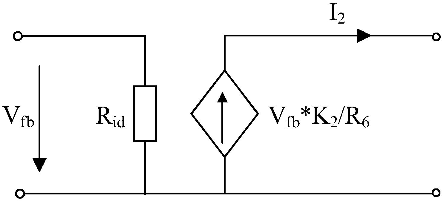
The harmonic offset loop consists of the following three parts: G1 contains an auxiliary CT2 and a current–voltage conversion circuit whose function is to isolate and collect the secondary current of CTX and then convert it into a voltage signal. The ratio of the auxiliary CT2 is K1, and the output current is I1, and the current I1 completely passes through the resistor R1, which is converted to the voltage Vfb = I1 ∙ R1, and according to the role of the integrated op–amp circuit, it can be seen that the output of the op–amp is the potential difference between voltages 2 and 3, which is also known as Vfb, and so the equivalent circuit diagram of G1 is as indicated in
Figure 2.
G2 contains two stages. The first stage is an amplifier circuit based on negative feedback, containing capacitor C2 and resistor R4, which further amplifies the output voltage of the G1 unit, with amplifier K2 = R4/R8. The second stage is a power amplifier circuit, which converts the voltage signal into current output. r6 is an output current sampling resistor, which is connected to the feedback loop to control the output current I2. I2 = Vfb ∙ K2/R6. The current output I2 of the G2 is the input of the G3 step-down transformer (rising current). The current output I2 of G2 is the input of the G3 transformer. The equivalent circuit diagram of G2 is as indicated in
Figure 3.
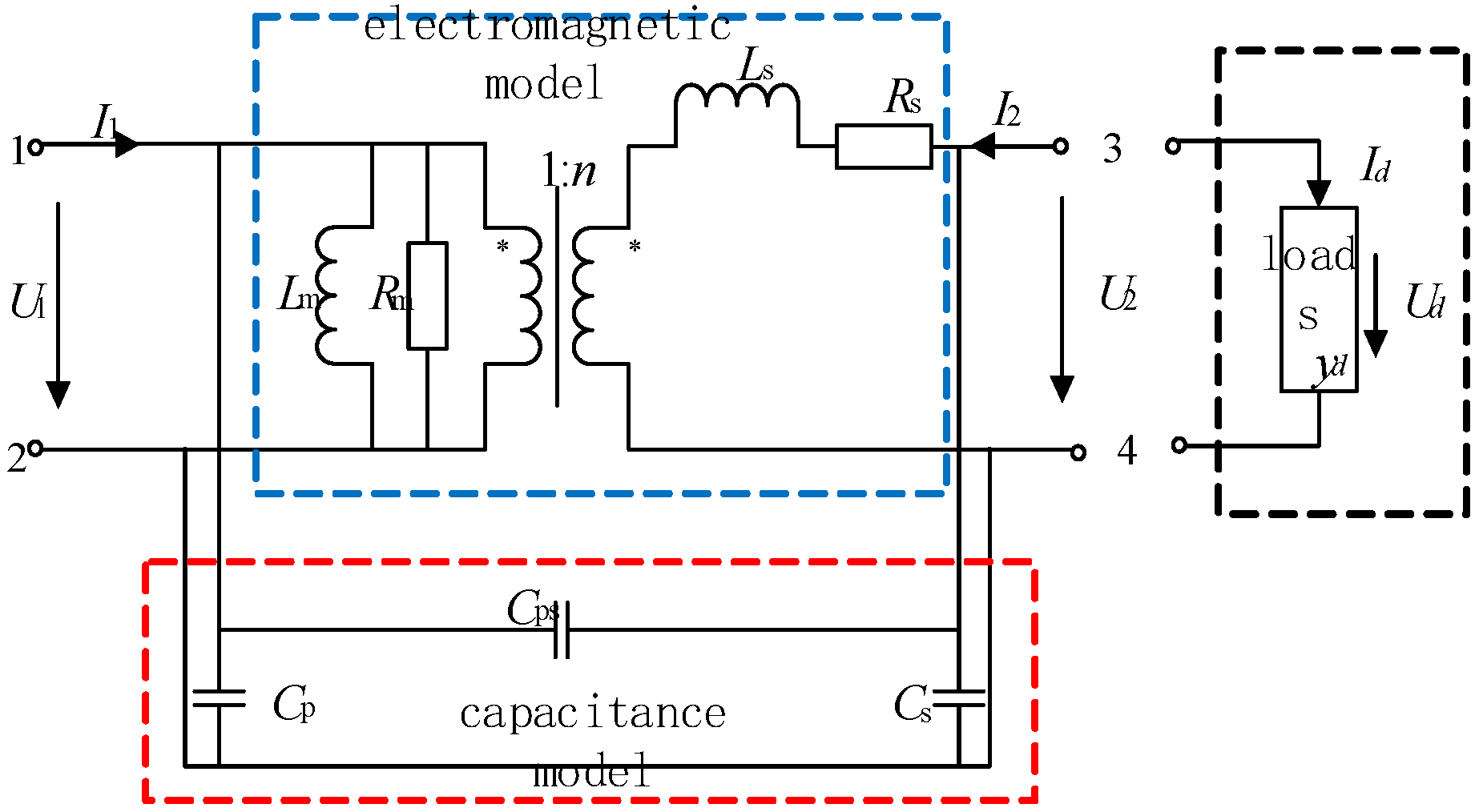
The G3 transformer can be viewed as a transformer and is modeled on the basis of an ideal transformer, taking into account stray capacitance and actual load.
As indicated in
Figure 4, the broadband mechanism model [
19] can reflect the electromagnetic coupling characteristics inside the high-frequency transformer, which is applicable to the optimization design.
Compared to the broadband mechanism model, the two-port equivalent model parameters in
Figure 5 are reduced from 15 to 7, and the model structure is more compact, which is applicable to the analysis of voltage and current characteristics of the primary and secondary winding ports of the high-frequency transformer.
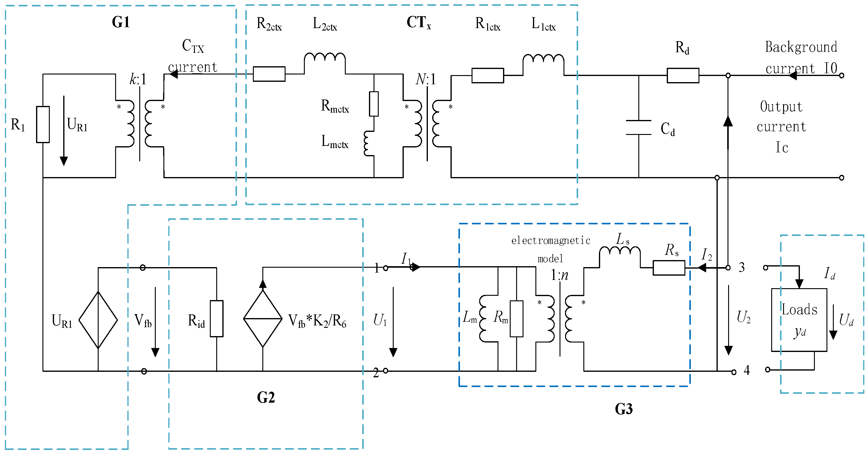
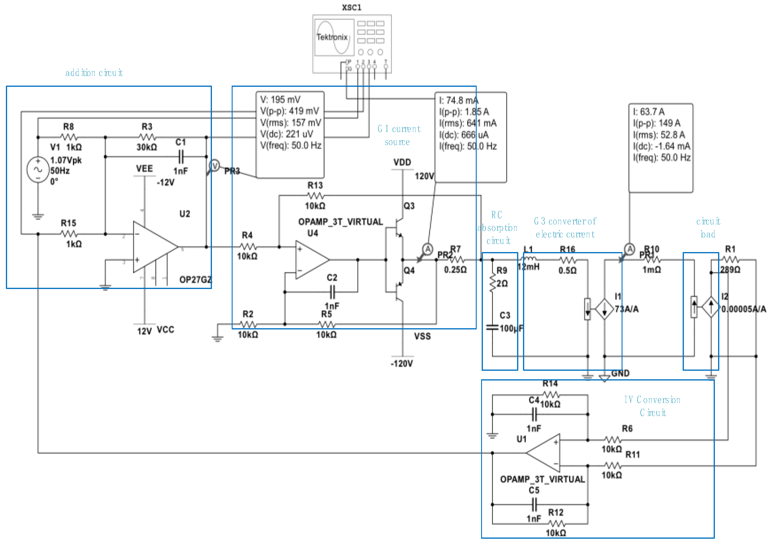
According to the above analysis, the equivalent circuit of the whole loop is shown in
Figure 6.
In G0(CTx), R1ctx and L1ctx are its primary side impedance, N is the variable ratio, R2ctx and L2ctx are its secondary side impedance, and Rmctx and Lmctx are its excitation impedance. Output CTx is a secondary current to G1. In G1, the CTx secondary current is changed to 1/k of the original and added to R1, the R1 voltage is UR1, and the voltage control voltage source outputs voltage Vfb = UR1. In G2, Rid is the input impedance of the operational amplifier circuit, and the voltage-controlled current source outputs the current I1 = Vfb ∙ K2/R6, and the reverse function is implemented. In G3, Lm and Rm are the excitation impedance of the transformer, n is the transformer ratio, and Ls and Rs are the leakage impedance, respectively.
Through the above equivalent circuit diagram, it can be found that when the parameters of all components and the load are fixed, the transfer function of the whole circuit is also fixed. When the load parameters change, the entire loop transfer function will also change.
As indicated in
Figure 7, the entire circuit designed from the above diagram is shown below.
According to the above figure, the transfer function of the entire loop can be derived, and the derivation process is as follows.
The figure shows that the input voltage of G1 is the voltage on the right side of R6, which is set as Ui, while the other port of G1 is grounded. Let the output voltage of G1 be U0, and then Ui and U0 satisfy the following relationship:
Then, let the input and output voltages in the addition circuit in G2 be Ui and U0, respectively, with the following relation:
Then, the output current of G2 is
Associating (2)–(4), the transfer function of the input voltage Ui and output current I1 for the combined G1, G2 circuit is
For the load side of the G3 loop, the resistance normalized to the primary side is much smaller than the primary side impedance, as can be seen from the G3 ratio and the loop load, so it can be ignored.
For the voltage ratio on both sides of the G3 module in
Figure 4,
where M2 is the mutual inductance of the transformer and L1 and L2 are the self-inductance of the primary and secondary sides of the transformer, respectively. Let the output current of G3 be I2, and according to the circuit diagram, the transfer function of the whole loop is:
The parameters are shown in
Table 1:
Substituting values gives:
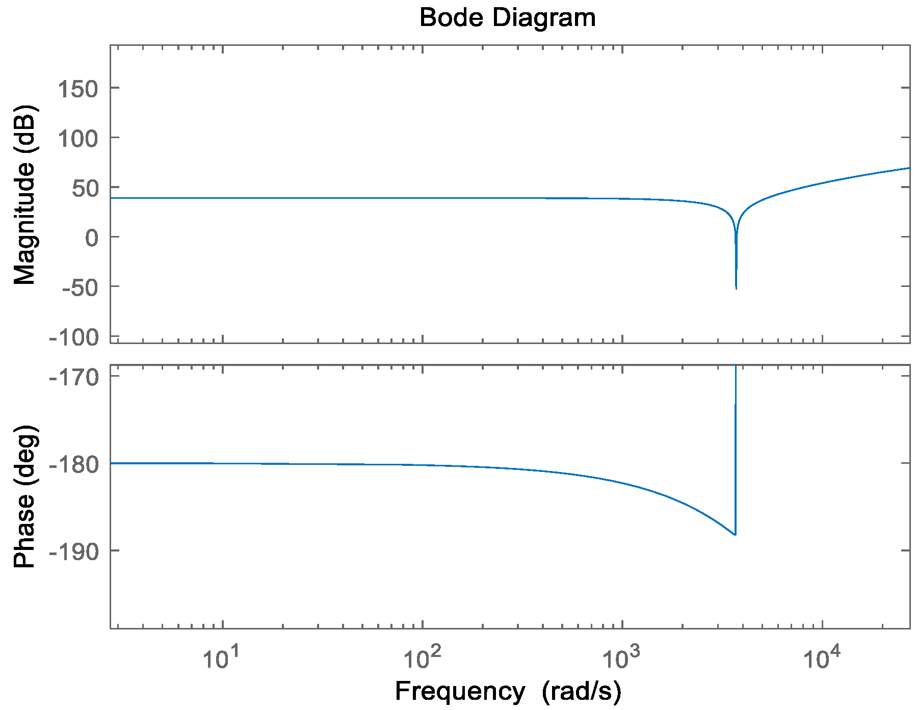
Magnitude–frequency plots show the magnitude response of a system at different frequencies. The horizontal axis usually represents frequency and the vertical axis represents magnitude (usually on a logarithmic scale); phase–frequency plots show the phase response of a system at different frequencies. The horizontal axis still represents the frequency, while the vertical axis represents the phase angle. The amplitude–frequency plot gives a clear picture of the response of the system to different frequencies, including the magnitude of the gain, the trend of the gain with frequency, etc. The phase–frequency plot gives an idea of the phase delay of the system to different frequencies, as well as the trend of the phase with frequency. After MATLAB processing, the following amplitude–frequency and phase–frequency plots can be obtained (
Figure 8).
From the bode plot, it can be seen that the amplitude–frequency characteristics and phase–frequency characteristics of the transfer function change as the frequency increases. At frequencies less than or equal to the third harmonic, the amplitude–frequency characteristics are a straight line, and the gain stabilizes at 40 db. The gain for the amplitude starts to change when the angular frequency is greater than 1000. And for phase, the gain changes when the corner frequency is greater than 15,000. From the baud plot, it can be seen that the existing design can satisfy the offset requirement for the third harmonic.
The background currents to be canceled also contain higher harmonics. For the offset of higher harmonic numbers, it is necessary to optimize the parameters of the whole loop and widen the bandwidth.
3. Optimization of a Calibration Device Based on the PSO Algorithm
Particle swarm algorithm is a commonly used heuristic algorithm in objective optimization problems. The algorithm combines the particle swarm algorithm (PSO) and multi-objective optimization techniques, which can find the best solution in different objective functions, solving the problems that cannot be solved by single-objective optimization algorithms and also avoiding the problem of local optimal solutions in multi-objective problems. The multi-objective particle swarm algorithm needs to fuse multiple objectives when dealing with multi-objective problems and improve the global optimality of the particles through weighted averaging. Specifically, the algorithm updates the positions and velocities of all particles in each generation, viewing each particle as a point to be searched in the objective function space. Extending the standard particle swarm algorithm, each particle has more than one position, which corresponds to the result of the multi-objective function. Each individual calculates the fitness value to adjust the particle position based on the current position and velocity, and updates the particle velocity. In addition, during the updating process, information is shared through communication between particles to help find a better solution. The advantages of the multi-objective particle swarm algorithm include strong global search capability, ease of implementation, faster convergence, and applicability to many types of problems. In this paper, the PSO algorithm is used to optimize the transfer function of the harmonic cancellation loop and the transfer function to be optimized is
Throughout the circuit, G3 plays a major role in transferring the characteristics. L2, L1, M2, LS0, Zs2, Zs1, C10, C20, C13, and C24 in Equation (8) affect the transfer characteristics. The objective particle swarm optimization algorithm was chosen to optimize the parameters of the offset device due to its advantages.
The optimization of the parameters of the entire loop requires the derivation of the magnitude and phase differences of the entire transfer function, which can be used as the objective function for optimization.
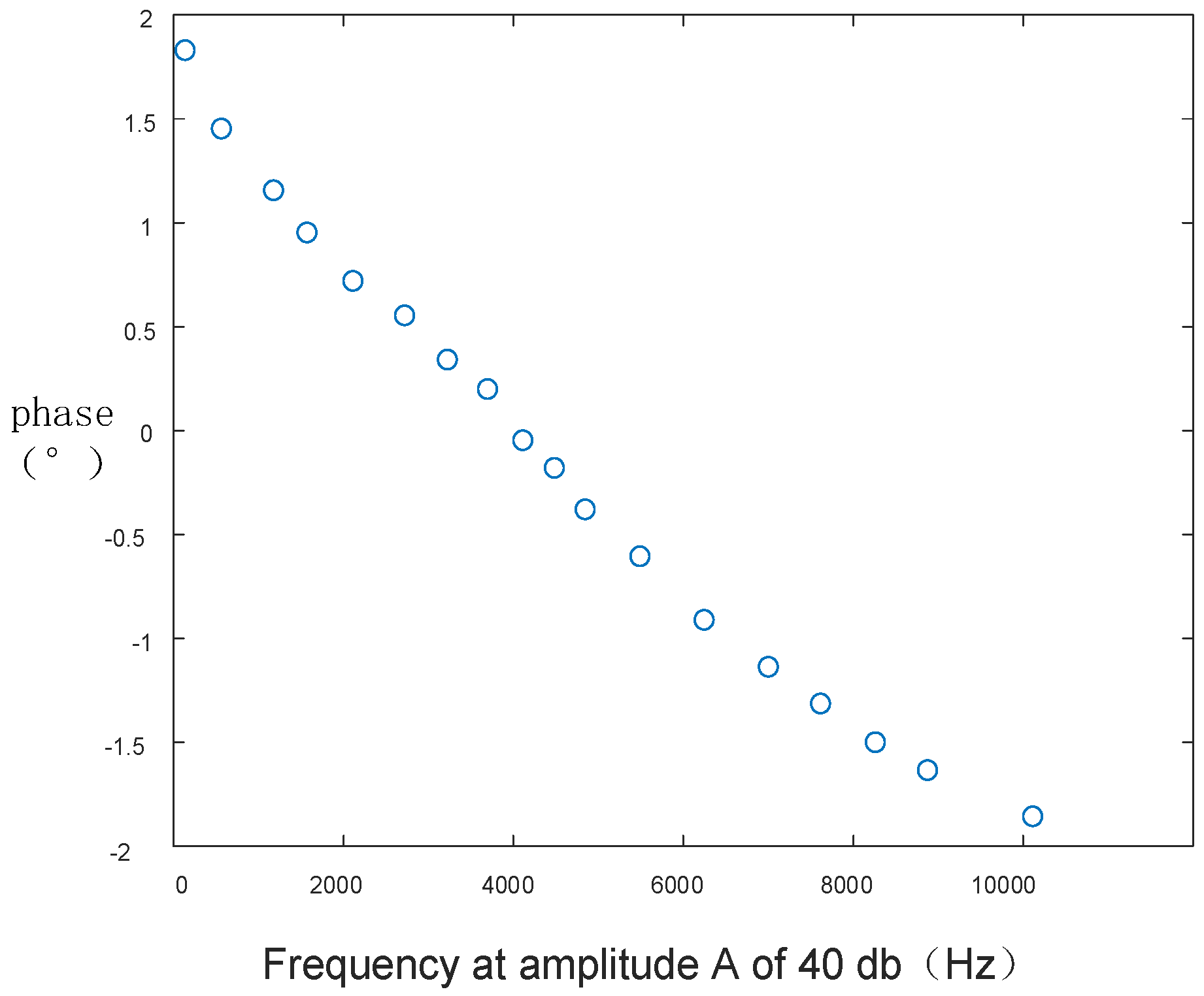
The objective function 2 is to find the maximum value of the frequency W when the amplitude A is taken as 40 db. The Pareto front of the optimized configuration scheme obtained by optimizing the parameters of the transfer function using PSO is shown in
Figure 9.
The optimized parameters are shown in
Table 2.
Substituting Equation (8) yields the optimized transfer function as
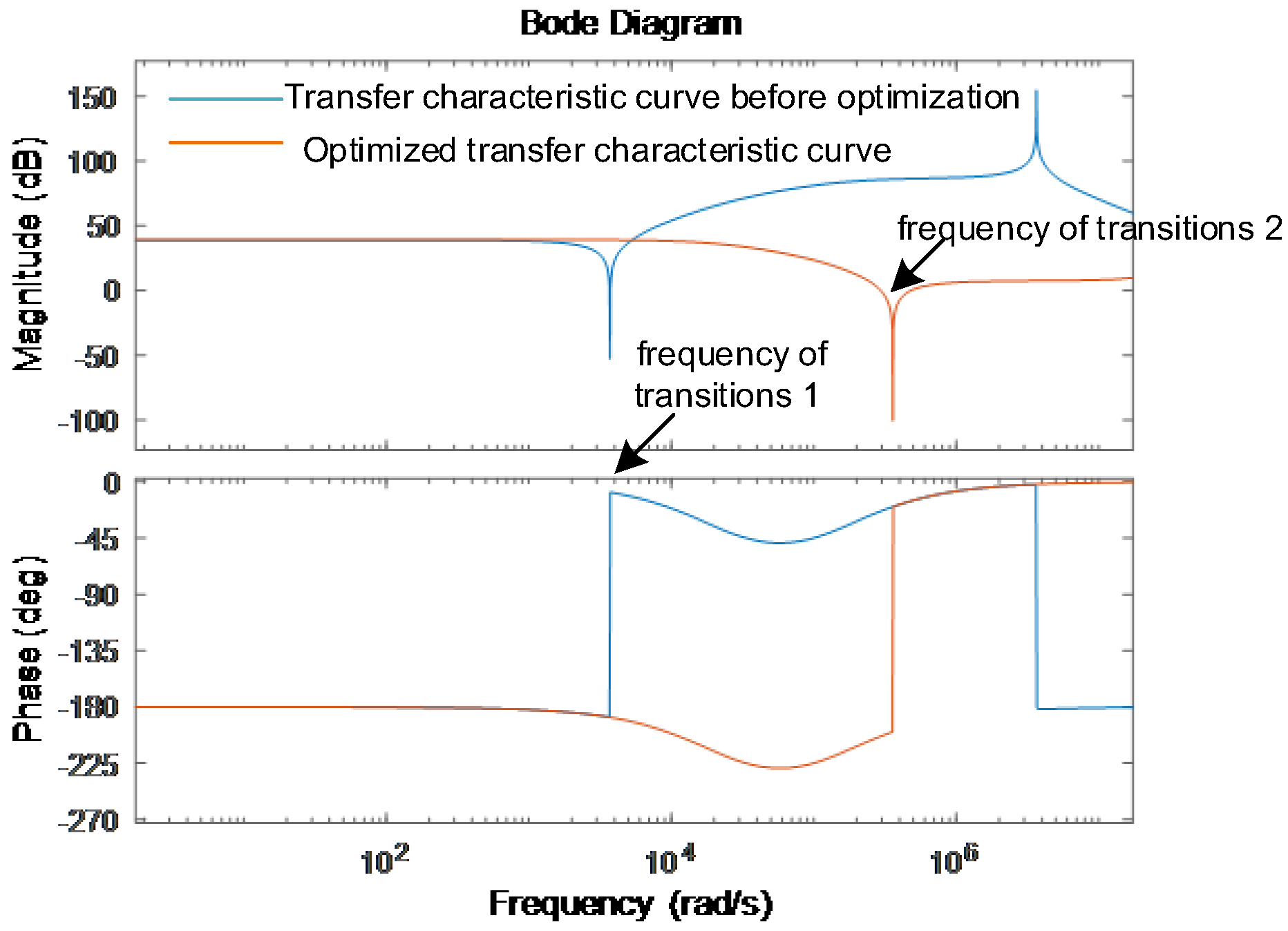
After MATLAB processing the following amplitude-frequency and phase-frequency plots can be obtained, as indicated in
Figure 10.
The red line is the optimized transfer function, the amplitude–frequency characteristic is a straight line when the frequency is less than or equal to the 200th harmonic, and the gain is stable at 40 db. From the theoretical analysis, the existing design can meet the requirements of 200th harmonic cancellation.
