Article

Dead-Time Inverter Voltage Drop in Low-End Sensorless FOC Motor Drives

by
Dionisis Voglitsis
1,*,
Massimo Paglia
2 and
Nick Papanikolaou
1
1
Electrical Machines Laboratory, Department of Electrical and Computer Engineering, Democritus University of Thrace, Kimmeria-Xanthi, 67132 Xanthi, Greece
2
CSS Division, Department of ICW MCU, Infineon Technologies AG, Am Campeon 1-15, 85579 Neubiberg, Germany
*
Author to whom correspondence should be addressed.
Energies 2024, 17(11), 2477; https://doi.org/10.3390/en17112477
Submission received: 13 March 2024 / Revised: 19 May 2024 / Accepted: 20 May 2024 / Published: 22 May 2024
(This article belongs to the Special Issue Advanced Control in Power Electronics, Drives and Generators)

Abstract

:
The purpose of this study was to investigate the impact of voltage drop of a three-phase voltage source inverter on driving brushless motors. This study also proposes an enhanced field-oriented control scheme that accounts for inverter voltage drop, enabling efficient driving at very low motor speeds. Experimental results are provided to verify the theoretical study and the proposed control scheme.

1. Introduction

Three-phase brushless motors have been at the forefront of the industry for more than three decades due to their efficiency and low cost. The technological development of microcontrollers in this period has enabled the implementation of sophisticated control schemes for motors that have been widely applied in the industrial sector [1]. Sensorless Field-Oriented Control (FOC) has been one of those control schemes and is probably the most popular among industrial motors. Compared to conventional control schemes, sensorless FOC provides efficient motor drive with fast dynamic response and better motor controllability, low current total harmonic distortion (THD), and reduced losses [2,3]. However, when it comes to applications where controllability at very low motor speeds is required, high-performance microcontroller units (MCUs) may be a prerequisite to addressing challenges related to reduced accuracy and reliability at low speeds or during startup, where sensor-less rotor position is particularly challenging. This challenge is intensified by the fact that the minimum stability margin often becomes critical at low speeds [4]. However, many residential and consumer electronic applications are sensitive to cost applications, and high performance MCUs cannot be easily afforded. Indicatively, household laundry motors with a gear ratio of 10 should work reliably down to 80 RPM using conventional inexpensive microcontrollers such as XMC13, XMC14, or PSoC4 from Infineon Neubiberg, Germany [5,6], STM32G0 family from ST Microelectronics Plan-les-Ouates, Switzerland [7], MSPM0G from Texas Instruments, Dallas, TX, USA [8], and LPC800 series from NXP Eindhoven, The Netherlands [9]. The constraints posed by low bandwidth, along with nonlinear voltage drops introduced by the driving system, as highlighted later in this study, and dead-time inverter voltage drops contribute to suboptimal controllability at low motor speeds. To address this problem, voltage drops are typically modeled as an average voltage loss over the switching period and compensated directly within the abc-reference frame [10,11,12,13]. This compensation involves integrating them into the reference voltages generated by the FOC scheme, before entering the Pulse Width Modulation (PWM) stage. Alternatively, the inverter voltage drop effect can be treated as a pulse shift error and directly compensated for in each PWM cycle [14,15]. Some works have proposed online compensation methods [16,17,18]. These methods are generally more intricate as they involve real-time estimation of the voltage drop, necessitating intensive computational processes (methods such as those described in [18], which employ online optimization algorithms that require significant processing power). In addition to online methods, some studies propose the self-commissioning characterization of the inverter during startup or when the motor is at a standstill [19,20,21,22]. In these works, the non-linearities of the inverter are estimated and stored in Look-Up-Tables (LUT) for subsequent compensation in the abc-reference frame. The techniques employed to generate these LUTs often involve current injection methods, such as applying a staircase current with a predetermined number of steps [20] or using an increase–decrease current injection technique [21]. An overview of control strategies to mitigate dead-time effect on converters is presented in [23].
Although the above works target motor drive applications, they do not consider low-end sensorless applications under dynamic conditions. Furthermore, achieving complete compensation of the inverter voltage drop is challenging due to nonlinearities such as parasitic capacitances [15], temperature variations [19], DC-link voltage variations, and so on. Therefore, as shown in this work, direct compensation at the abc-reference frame in low-end sensorless applications may be inadequate, resulting in suboptimal performance at low speeds due to insufficient compensation during dynamic conditions. Instead, it may be beneficial to address compensation for inverter voltage drops at the flux observer stage within the FOC framework, where system dynamics are better considered than at the abc-reference and PWM stages. Such an attempt is made in [24], where a self-commissioning inverter characterization technique is proposed to identify and subsequently compensate the inverter non-linearities at the observer stage. A current is injected by the inverter during startup (when the motor back electromotive force (EMF) is zero) to identify and store inverter non-linearities. These identified nonlinearities are stored in an LUT for subsequent compensation. A similar attempt was made in the current work, where voltage drops were compensated for at the flux–observer stage using an LUT. A key distinction from the work presented in [24] lies in the fact that, in the current study, the voltage drops are normalized within the αβ-reference frame offline (without any characterization process involved) and pre-stored in an LUT. Subsequently, based on the sign of the inverter current, voltage drops are retrieved from the LUT and employed within an αβ-reference frame at the flux–observer stage. While the proposed technique may not address all the nonlinearities of the inverter, it offers a straightforward solution ensuring effective motor control across a broad speed range. Additionally, this is a computationally inexpensive and fully compatible low-cost microcontroller solution, as it requires only a 64-byte LUT to represent the inverter voltage drops in the αβ-reference frame as part of the FOC scheme. Moreover, when the motor reaches a certain speed, the impact of voltage drops dilutes; therefore, the controller disables the proposed voltage drop compensation, transitioning into a conventional FOC controller. The entire FOC control scheme, including the proposed methodology, was implemented with an inexpensive 40 MHz 32-bit ARM® Cortex®-M0+ microcontroller with 64 kB and 8 kB RAM, and experimentally tested for a low-end motor of 545 W nominal power. Simulation and experimental results are presented to verify the effectiveness of the proposed methodology. The obtained results support this method as a promising solution for low-end brushless motor drives.
To conclude, this paper studies the inverter voltage drop phenomenon in low-end motor drives. It also proposes a methodology to account for voltage drop, improving the controllability of brushless motors at low speeds. The proposed methodology can be easily implemented with inexpensive microcontrollers, such as ARM® Cortex®-M0 microcontrollers [5,6,7,8,9].
The rest of the paper is organized as follows: In Section 2, the system under study is described. In Section 3, the principle of the FOC algorithm is presented. In Section 4, the voltage drop of the inverter is theoretically analyzed and modeled and the proposed methodology is presented. Section 5 and Section 6 present simulation and experimental results, respectively. Finally, Section 7 concludes the paper, and ideas for further applications are suggested.

2. System under Study
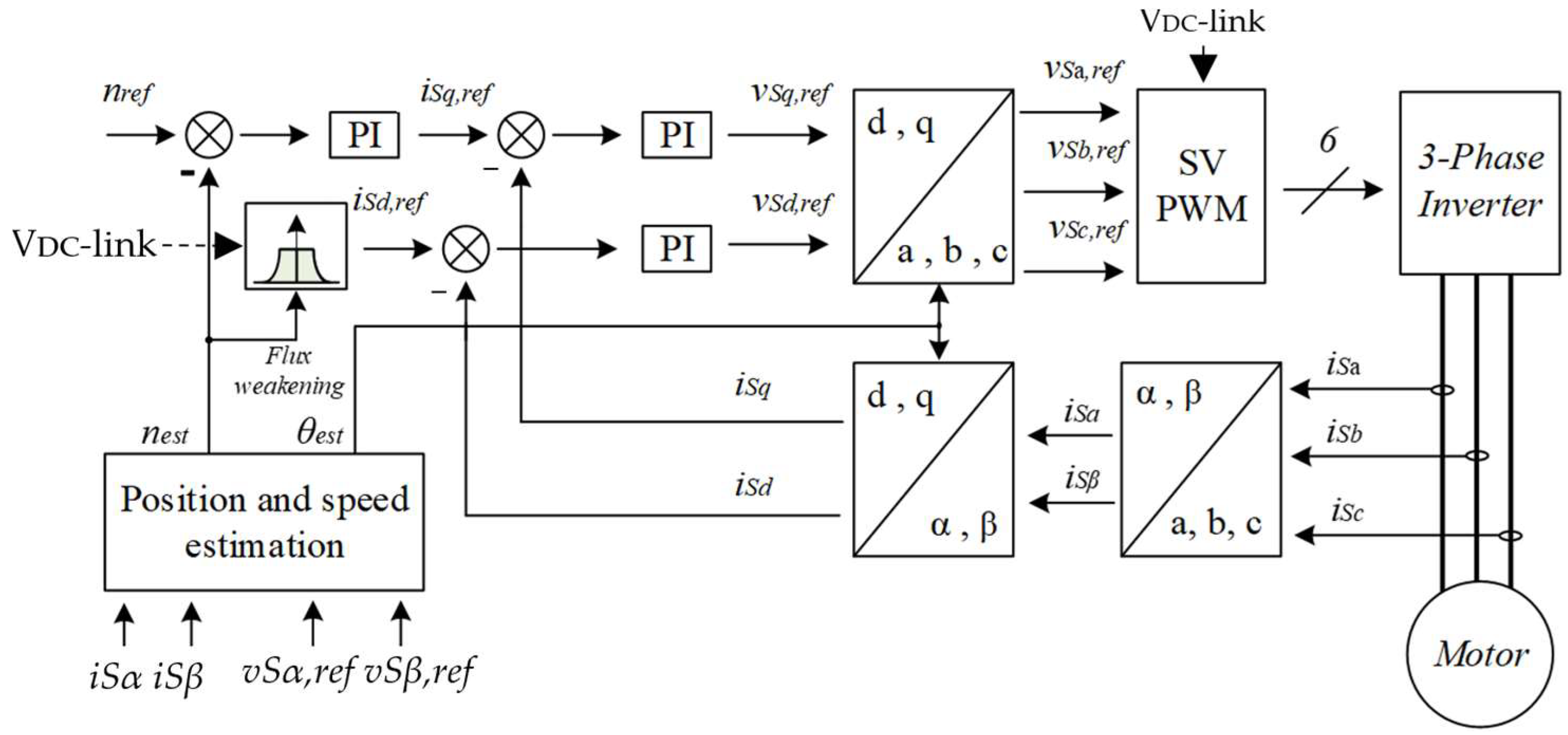
The system under study is illustrated in Figure 1. It contains the conventional architecture of a low-power motor drive system comprising four subsystems/stages. The mandatory electromagnetic compatibility filter stage was omitted from the description. The first subsystem is the Power Factor Correction (PFC) converter. The main task of the PFC is to provide a regulated output voltage and improve the grid AC current’s Total Harmonic Distortion (THD). In this work, a two-channel interleaved boost PFC converter was used, maintaining a close to unity power factor (PF), low THD, and 400 V regulated output voltage via a proper voltage regulation and power factor correction control scheme.
The second subsystem is the inverter, which is the subject of our work. In this work, a three-phase two-level voltage source inverter (VSI), typical of motor drive applications, was used. The DC input of the inverter is connected to the PFC subsystem, while its output is directly connected to electric motor stator windings. VSI is controlled via a low-end MCU.
The MCU is the third subsystem. Typically, the MCU is a conventional low-end microcontroller that provides a PWM peripheral, along with an analog-to-digital (ADC) peripheral and a serial communication peripheral. As previously noted, the MCU used in our work is a 40 MHz ARM® Cortex®-M0+ microcontroller equipped with 64 kB flash memory and 8 kB RAM. The ADC module boasts a 12-bit ADC channel capable of handling a maximum conversion rate of 1.2 million samples per second, whereas the achieved Pulse Width Modulation (PWM) accuracy was measured at 10.29 bits.
The final subsystem is the driving unit, which encompasses a motor linked to a mechanical load. This study focuses on applications that require low-end motors such as residential laundry appliances and air compressors.

3. FOC Description

This section describes the FOC control scheme. Figure 2 illustrates the typical block diagram of a sensorless FOC [3], where the term sensorless refers to the method of estimating motor speed and position. In other words, the rotor’s position (θest) and speed (nest) are not directly measured but estimated/calculated. It is also worth noting that according to Figure 2, FOC enables the control of motor speed directly from the q-component of the motor current, while the d-component of the motor current is directly related to the flux produced by field windings. Severing the direct relationship between motor speed and the d-component of motor current yields significant advantages in terms of control. In this study, an initial DC current was injected into the motor stator windings during startup, thereby orienting the rotor to its initial position. This approach effectively decouples motor control parameters.
In the current work, the position (θest) and speed (nest) were estimated with the aid of a reduced order flux observer, akin to the one described in [25]. This method provides a robust low-complexity solution with good dynamic control and wide speed range operation, even in the presence of parameter variations and measurement noise. The flux observer receives as input the motor current and VSI reference voltages in an αβ-reference frame while generating the estimated motor speed and position as output. The motor speed is controlled via a Proportional Integral (PI) controller. The PI controller maintains the estimated speed at the speed reference value nref. The output of this PI controller was used as the input reference q-component of the motor current. The measured and referenced q-components were fed to a second PI, the output of which was used to generate the reference value of the q-component of the inverter reference voltage. When flux weakening is not engaged, the reference value of the motor current’s d-component is set to zero (0.0). The d-component is controlled via a third PI controller, whose output generates the d-component of the VSI reference voltage. The generated dq-components of the voltage reference of VSI are transformed back to abc quantities with the aid of inverse Park and inverse Clark transformations. These time-variant voltage quantities are considered the output of the FOC control scheme. They are fed to the PWM module of the MCU along with the DC-link voltage to generate an appropriate switching pattern that will drive the insulated gate bipolar transistors (IGBTs) of the VSI. The modulation strategy used in the current work was based on bipolar PWM, while a third harmonic injection was used to boost the DC-link utilization level afterward. Once the switching pattern is applied to the IGBTs, the inverter should generate the desired AC voltage to drive the motor.
In Figure 2, the FOC block diagram incorporates the flux weakening component as well. However, since the analysis in this paper focuses on low motor speeds, the following discussion omits an explanation of flux weakening. For a more comprehensive understanding of flux weakening, readers can consult relevant references [26,27].

4. Inverter Voltage Drop Modeling

4.1. Basic Analysis of Inverter Voltage Drop

As mentioned in the introduction, when the FOC algorithm attempts to control the motor at very low speeds, the voltage generated by the inverter is in the same order of magnitude as the inverter voltage drop, significantly affecting the estimated speed and position of the rotor. This results in poor performance for the flux observer and eventually for FOC. For typical sensorless low-end applications, the inverter voltage drop is the bottleneck of low-speed control. In this section, we elaborate on this problem by analyzing the VSI output voltage and the voltage drop that occurs due to the non-ideal characteristics of the inverter, We also propose a solution to increase motor controllability at low speeds.
Due to the intrinsic characteristics of the IGBTs and diodes as well as the switching modulation pattern of the inverter, there was a voltage drop across the inverter output. This drop primarily derives from:
  • IGBTs/diodes conduction and switching losses such us IGBT forward voltage and on-state resistance and diode forward voltage drop;
  • PWM dead time.
The voltage drop from IGBTs/diodes conduction and switching losses depends on the motor current and their bespoken inherent characteristics. The voltage drop from PWM dead-time depends on dead-time duration and DC-link voltage level. For single-phase applications, where the DC-link voltage of VSI is typically boosted around 400 V, PWM dead time is the predominant factor of VSI voltage drop.
With the aid of the circuit in Figure 3, we can gain a better understanding of the physical representation of the inverter’s output voltage and voltage drop. Each leg of the inverter generates a voltage with respect to node “o” (i.e., vxo) and a voltage with respect to node “m” (i.e., vxm), where “x” denotes the inverter phases a, b, and c. The output voltage of the inverter, hereafter vxo, is dictated by the switching pattern of IGBTs and the DC-link voltage. As previously noted, the DC-link of single-phase applications is typically regulated by the previous stage (via the PFC) to around 400 V. The switching pattern of the inverter is dictated by the modulation strategy (PWM, space vector modulation, discontinuous PWM, etc.), the reference voltage quantities vsa,ref, vsb,ref, vsc,ref, which are generated by the FOC scheme, and the peripheral configurations of the MCU (PWM resolution, single-edge/symmetrical-mode, etc.). Although FOC generates symmetrical sinusoidal reference quantities, the inverter output voltage, vxo, and the voltage applied to motor winding, hereafter, vxm, contain high-frequency components due to the modulation switching pattern. Due to VSI topology and the modulation strategy, a high-frequency voltage is also generated at vmo. The relationship between vxo, vxm, and vmo is defined by the following equation:
v x m t = v x o t v m o t = v x o t v a o t + v b o t + v c o t 3
To exclude high-frequency ripples from our analysis, we adopted a switching average model [28]. The equation below, in which “*” represents switching average quantities, demonstrates the mathematical approach behind switching average modeling:
v t * = 1 T P W M t t + T P W M v t d t
Applying the switching average approach to Equation (1), we obtain the following expression:
v x m t * = v x o t * v a o t * + v b o t * + v c o t * 3
Assuming the case of an ideal inverter without voltage drop, v x o can be rewritten as:
v x o t * = 2 d x t * 1 · V D C 2
where, dx(t)* (0 ≤ dx(t)* ≤ 1) denotes the percentage of the switching period at which the upper IGBTs are turned on; dx(t)* is the control input signal to our model, whose value is dictated by the FOC controller.
In the case where the inverter is ideal, the sum of vao(t)* + vbo(t)* + vco(t)* is zero (0.0), as FOC generates in principle three-phase symmetrical reference voltages; therefore:
v x m t * = v x o t *
In summary, in the case of dead-time-free operation, the switching average voltage applied at the windings of the motor (vxm) is controlled directly by the reference voltage generated by the FOC.
When the inverter is not ideal, the sum of voa(t)* + vob(t)* + voc(t)* is not zero (0.0) because vxo(t)* also includes the inverter voltage drop. At low motor speeds, the motor driving voltage is low, and the dead-time period of the inverter becomes the main source of voltage drops. In power conversion systems, dead time refers to the mandatory period during which the switching elements of the same inverter leg must be simultaneously turned off before each transition, to prevent short-circuiting the inverter.
To understand the rationale behind the distortion in the generated voltage, it is essential to first delve into the influence of dead time on the inverter output voltage, vxo. In Figure 4 and Figure 5, the discernible impact of asymmetric (keeping the turn-off edges intact) dead time on inverter voltage vxo* is evident.
Considering circuitry analysis in Figure 3 and current flow analyses in Figure 4 and Figure 5, the following equations regarding the inverter output voltage were developed:
If the current of x-phase is positive:
v x o t * = 2 d x * t 1 2 · d e a d   t i m e T P W M · V D C 2
If the current of x-phase is negative:
v x o t * = 2 d x * t 1 + 2 · d e a d   t i m e T P W M · V D C 2
We can observe that vxo(t)* contains an additional part that depends on the direction of the corresponding phase current. This additional part, hereafter called inverter voltage drop, is uncontrolled and depends on DC-link voltage, PWM dead time, PWM frequency, and the direction of the corresponding phase current. The resistance of switching elements (rds-on) and non-linearities such as parasitic capacitance [15] and switching elements junction–temperature [19] also affect voltage drop; however, they are not considered in this study. To distinguish the uncontrolled part from the inverter output voltage controlled via the FOC, we used the following two conventions: The term vxo,FOC(t)* represents the component controlled via the FOC scheme, and the term vxo,drop(t)* represents the uncontrolled voltage drop component:
v x o , F O C t * = 2 d x t * 1 V D C 2
v x o , d r o p t * = + d e a d   t i m e T P W M · V D C , i S x ( t ) < 0 d e a d   t i m e T P W M · V D C , i S x ( t ) > 0
the sign of which depends on the x-phase current of the motor, iSx(t).
Based on Equation (9), the magnitude of the inverter voltage drop depends on the PWM period, PWM dead time, and the inverter DC voltage. Since those parameters are typically fixed for each application, the following constant can be used to benchmark the inverter voltage drop:
V d r o p = d e a d   t i m e T P W M · V D C
Having defined vxo(t)*, we can define the voltage across the motor winding as:
v x m t * = v x o , F O C t * + v x o , d r o p t *   v a o , F O C t * + v b o , F O C t * + v c o , F O C t * + v a o , d r o p t * + v b o , d r o p t * + v c o , d r o p t * 3
As FOC generates symmetrical three-phase voltages, Equation (11) is rewritten as:
v x m t * = v x o , F O C t * + v x o , d r o p t * v a o , d r o p t * + v b o , d r o p t * + v c o , d r o p t * 3
Similar to vxo(t)*, the switching average voltage applied across the motor winding, vxm(t)* consists of two parts: A part that is directly controlled by FOC and an additional part that depends on inverter voltage drop and cannot be directly controlled. This additional part will be hereafter named motor winding voltage drop, denoted as vxm,drop(t)*:
v x m , d r o p t * = v x o , d r o p t * v a o , d r o p t * + v b o , d r o p t * + v c o , d r o p t * 3
Assuming that the motor is fed with symmetrical sinusoidal three-phase currents, the value of vao,drop(t)* + vbo,drop(t)* + vco,drop(t) equals to ±Vdrop, where the sign depends on the signs of the phase currents (Table 1):
v a o , d r o p t * + v b o , d r o p t * + v c o , d r o p t * = d e a d   t i m e T P W M · V D C = V d r o p
In summary, by applying Equation (14) to Equations (9) and (13), we derive the normalized values of the inverter and motor winding voltage drop, vao,drop(t)* and vam,drop(t)*, respectively. The values for phase a are plotted against time in Figure 6 using Vdrop in Equation (10) as the base value, assuming that the motor is fed with the arbitrarily selected symmetrical sinusoidal three-phase currents in the top graph. Similar values can be obtained for the remaining b and c phases.

4.2. Voltage Drop: Modeling in the aβ- and dq-Synchronous Reference Frames

This subsection represents the voltage drop in the αβ0- and dq0-reference frames. This representation is very useful, as it will be used later to integrate them into the existing FOC scheme (Section 5).
Typically, the dq0 transformation used in FOC schemes is the amplitude-invariant version. Also, the d-component is usually aligned with phase a of the inverter reference voltage. The amplitude-invariant dq0-transformation, which aligns phase a with the d-component, is achieved using the well-known matrix in Equation (15). For q-component alignment, alignment with phases b and c, or power-invariant transformation, the appropriate matrixes should be applied. However, the subsequent analysis remains valid.
d q 0 = 2 3 cos θ cos θ 2 π / 3 cos ( θ + 2 π / 3 ) sin θ sin θ 2 π / 3 sin ( θ + 2 π / 3 ) 1 / 2 1 / 2 1 / 2 a b c
Similarly, for phase-a alignment, the amplitude invariant αβ0-transformation is achieved by using the matrix below:
α β 0 = 2 3 1 1 / 2 1 / 2 0 3 / 2 3 / 2 1 / 2 1 / 2 1 / 2 a b c
To obtain the αβ0- and dq0-components of the motor winding drops vxm,drop(t)*, we used [a;b;c] as input, the quantities [vam,drop(t)*, vbm,drop(t)*, vcm,drop(t)*]. For the αβ0- and dq0-transformations of inverter voltage drops vxo,drop(t)*, we used [a;b;c] as input, the quantities [vao,drop(t)*, vbo,drop(t)*, vco,drop(t)*]. After algebraic computations, we can conclude the following:
v d v x m , d r o p t * d q 0 = v d v x ο , d r o p t * d q 0 ; v q v x m , d r o p t * d q 0 = v q v x ο , d r o p t * d q 0 v a v x m , d r o p t * a β 0 = v α v x ο , d r o p t * α β 0 ; v β v x m , d r o p t * a β 0 = v β v x ο , d r o p t * α β 0 v 0 v x m , d r o p t * d q 0 = v 0 v x m , d r o p t * a β 0 = 0 ; v 0 v x ο , d r o p t * d q 0 = v 0 v x ο , d r o p t * a β 0
Figure 7 illustrates the αβ0- and dq0-components of inverter and motor winding voltages, considering that the motor is fed with arbitrarily selected symmetrical sinusoidal three-phase currents in the top graph. Please note that the 0 component of the winding motor voltage drop is zero (0.0) both in αβ0- and in dq0-transformations, while the 0 component of the inverter voltage drop is a square waveform with a frequency of three times the fundamental frequency.
Finally, the dq-components of the inverter output voltage and the motor winding voltage drop have both a dc part and an alternating part. The former represents voltage drops in the grid frequency, while the latter represents high-frequency ripple drops (six times the fundamental frequency). The dq- and αβ-components refer to motor windings that must be considered in the FOC control scheme. In particular, the αβ-components were inserted into the flux observer in Figure 2 to account for the inverter voltage drop. The following paragraph describes the proposed methodology.

4.3. Voltage Drop: Insertion into FOC aβ-Reference Frame

Substituting the [a;b;c] components of Equation (16) with the obtained values of vxm,drop(t)* and vxo,drop(t)* in Table 1, we obtain the following LUT (Table 2):
The proposed methodology is depicted in Figure 8. DC-link voltage, dead-time interval, and switching period are used to calculate Vdrop magnitude. The dead-time interval and switching period represent constant parameters contingent on the application. On the other hand, even though the DC-link voltage is maintained at a fixed value through PFC regulation, it may exhibit fluctuations due to the finite bandwidth control of the PFC and inverter modulation. However, in three-phase systems, the fluctuation of the DC-link voltage is minimal and largely mitigated using electrolytic capacitors at the inverter input. Given the gradual nature of DC-link voltage dynamics, Vdrop update frequency can be set quite low, such as 10 Hz.
The estimated Vdrop and motor current were employed to derive the αβ-components of the voltage drop. Subsequently, these components are combined with the αβ-components of the inverter reference voltage and fed into the flux observer block. As described later, incorporating voltage drop into the flux observer block is beneficial because the observer’s dynamic response is accounted for more effectively.

5. Simulation Results

This section presents the simulation results of our proposed enhanced FOC methodology for driving a 4-pole-pair brushless motor. The system was simulated in Matlab-Simulink 2021a®, omitting the PFC stage and electromagnetic compatibility (EMC) filter. The chosen VSI topology employs a three-phase B6 configuration, as illustrated in Figure 1. The input voltage of the inverter was set to 400 V. The inverter as well as the motor characteristics used for the simulation are listed in the table below.

5.1. Proposed Voltage Drop Compensation Scheme

Figure 9 demonstrates the positive impact of our proposed methodology. Specifically, it showcases a scenario where the motor is commanded to achieve 82 rpm from a standstill position under maximum loading. The simulation involved three cases:
  • In the top graph, the system operates ideally with no dead time introduced;
  • In the middle graph, the system is non-ideal, featuring a 2 us dead time but without any compensation method;
  • In the bottom graph, the system is non-ideal and incorporates a 2 us dead time while applying our proposed compensation method.
It is evident that without compensation, the motor fails to start up under realistic dead-time values.

5.2. Comparison between abc-Voltage Drop Compensation and αβ—Reference Voltage Drop Compensation

In Figure 10, the FOC response is depicted for different dead-time cases, with compensation applied to the voltage drop at the abc-reference frame at the PWM stage. The simulation scenario showcases the motor being commanded to reach 82 rpm from a standstill position under maximum loading. These results are based on the system parameters outlined in Table 3. Based on the results, the flux observer encounters significant fluctuations even with a dead time of 1.5 us. By contrast, the motor fails to start up at all for dead times exceeding 1.9 us.
On the other hand, Figure 11 shows the results of applying the proposed methodology to the above simulation scenario. Notably, the flux observer demonstrates significantly reduced fluctuations, whereas the motor can start up and sustain a speed of 82 rpm, even with a high dead time of 2 us.
Lastly, Figure 12 provides a comparative overview of motor controllability at low rpm. The comparison was made based on 2 us dead time for three scenarios: (a) without compensation; (b) compensation at the abc-reference frame; and (c) the proposed methodology involving voltage drop compensation at the αβ-reference frame. The superior performance of the proposed methodology is evident based on the showcased results.

5.3. Enhanced FOC Validation over the Entire Motor Speed Range

Lastly, we present results for the proposed enhanced FOC used to drive the motor across the entire speed range (0–7000 rpm). The motor initially accelerated at a rate of 560 rpm/s until it reached 7000 rpm. Beyond 1000 rpm, the proposed voltage drop compensation was deactivated. Flux weakening came into effect at around 6000 rpm and remained engaged until the motor speed fell below this threshold during the deceleration phase. After the motor reached its maximum speed, it maintained this speed for ~10 s before being commanded to decelerate to 82 rpm, with the deceleration rate set again to 560 rpm/s. The proposed methodology was reactivated as the motor speed dropped below 1000 rpm. The motor effectively attained and sustained the target speed of 82 rpm for approximately 7.5 s. Figure 13 illustrates the described scenario, and includes two subfigures providing a closer view of the motor start-up and final commanded speed.

6. Experimental Results

This section presents the experimental results of an actual motor drive system. A test bench was constructed to validate the proposed voltage drop compensation method. The experimental setup is depicted in Figure 14. It contains the following subsystems (as described in the Introduction):
  • The EMC filter;
  • The PFC;
  • The VSI;
  • The MCU;
  • The driving system.
For this study, the SECO-1KW-MCTRL-GEVB evaluation board provided by onsemi Scottsdale, AZ, USA, was used [29]. This board incorporates both PFC and VSI stages, along with an electromagnetic compatibility filter. The PFC stage comprises a single-phase passive rectifier and a two-channel boost converter. Conversely, VSI employs a traditional three-phase B6 configuration, common in motor applications. The VSI is built using the Intelligent Power Module (IPM) AND9390/D, a specialized integrated circuit (IC) tailored for three-phase motor applications developed by onsemi [30]. The board is also equipped with a convenient connector designed for external control of the VSI IGBT gate drivers. The complete board layout, encompassing the electromagnetic compatibility filter, is illustrated below. Positioned at the bottom of the evaluation board, one may notice the control board housing the MCU.
Regarding the MCU, a low-end ARM® Cortex®-M0+ microcontroller was used. This MCU has a flash memory of 64 kB and a 40 MHz clock. It also comes with Direct Memory Access (DMA), a PWM peripheral, a 12-bit 1.2 M samples/sec ADC peripheral, and timer modules, which were used for FOC implementation. The MCU board is also outfitted with suitable connectors designed to interface with the evaluation board. As shown in Figure 15 (right photo), the MCU board is affixed to the underside of the evaluation board.
Finally, regarding the driving system, two mechanically coupled 545 W 4-pole-pair brushless AC machines from Bosch were used, where one machine operated as a motor and the other as a generator (see Figure 14). The generator was loaded via a three-phase variable resistive network, behaving as an equivalent variable mechanical load. Table 4 provides an overview of the foremost technical specifications of the system.

6.1. Start-Up to Low-Speed Validation

This section assesses the effectiveness of our proposed method under low-speed operations. When the motor operates at low speed, the voltage drop effect is critical. The controller encounters the most significant challenges at low speed, specifically when the motor is commanded from a stalled position to achieve minimal speed under the influence of maximum loading. As such, Figure 16 showcases a scenario where the stalled motor is commanded to reach 82 rpm under heavy loading conditions. This transition is reflected in the shorting of the three-phase resistor network, simulating a heavily loaded operational state.
The scenario described above, which involves the motor being commanded to reach 82 rpm from a stalled position, was replicated without applying our proposed compensation methodology. Figure 17 and Figure 18 provide insight into the motor current. Consequently, the motor loses synchronization and cannot start up.
Finally, Figure 19 and Figure 20 present results from the graphical user interface (GUI) used during the experiment. Figure 19 provides insight into crucial controller parameters when the motor is at a standstill and commanded to reach 380 rpm under maximum loading with our proposed methodology. Figure 20 shows the same scenario without our methodology. In the absence of compensation, the motor fails to initiate when dead time is introduced.

6.2. Deceleration to Low-Speed Validation

In this section, we explore a scenario where the motor decelerates to a speed of 82 rpm. Figure 21 and Figure 22 depict the motor’s current behavior as it decelerates from 400 rpm to 82 rpm using our proposed voltage drop compensation methodology. It is evident from these figures that the motor effectively achieves and maintains the desired lower speed as commanded.
A similar scenario is depicted in Figure 23, where GUI results illustrate the d and q components of the motor current along with other crucial controller parameters. In this scenario, the motor runs at 1000 rpm and is then commanded to decelerate to 82 rpm under maximum loading.

6.3. High Speed Validation

In this section, the proposed enhanced FOC scheme was tested over the entire motor speed range. Beyond 6000 rpm, the VSI reaches its nominal voltage, and flux weakening is engaged. Beyond 2000 rpm, as described in Section 4.3, the impact of voltage drop becomes less significant, and the controller deactivates the proposed methodology, transitioning to a conventional FOC scheme.
Figure 24 illustrates the motor dq current components along with the reference motor speed in rpm, the flux observer estimated speed in rad/s, and the DC-link voltage. The results showcase the scenario where the motor accelerates from 400 rpm to 6000 rpm. Figure 25 showcases the scenario where the motor accelerates from 7100 rpm to 9000 rpm. Flux weakening engagement is evident from the growth in the d-component of the motor current. Finally, Figure 26 and Figure 27 show the actual motor current while the motor operates at 8500 and 9000 rpm, respectively.
The results presented signify effective motor controllability over the entire motor speed range, including the engagement of flux weakening and the disengagement of the proposed methodology.

7. Conclusions

In this work, an enhanced FOC scheme accounting for inverter voltage drop is proposed, enabling the efficient drive of brushless machines at very low motor speeds. Regarding the motor’s controllability, inverter voltage drops have been shown to play a significant role in low-end microcontrollers. The controller performance is strongly affected by inverter voltage drop and the low control bandwidth of conventional MCUs, driving the motor unreliably in the low-speed range. Based on the presented results, the proposed methodology mitigates this problem because it accounts for voltage drops within the FOC control scheme. At higher speeds where the impact of the voltage-drops is less significant the proposed methodology deactivates and the controller transitions to a conventional FOC controller. The experimental results verified the controller’s excellent performance up to 9000 rpm and down to 82 rpm. As the next step, the effectiveness of this method will be verified through real application use cases to consider actual dynamic conditions, such as the drum dynamic of a washing machine.

Author Contributions

Conceptualization, D.V. and M.P.; methodology, D.V.; software, D.V. and M.P.; validation, D.V. and M.P.; writing—original draft preparation, D.V.; writing—review and editing, D.V., N.P. and M.P. All authors have read and agreed to the published version of the manuscript.

Funding

This research received no external funding.

Data Availability Statement

Data are contained within the article.

Acknowledgments

We would like to express our gratitude to the Department of Solution Engineering Center of Onsemi in Munich, particularly Martin Embacher for their invaluable assistance in conducting this work and for their generous provision of hardware, including the SECO-1KW-MCTRL-GEVB evaluation board, motor-generator system, and essential laboratory equipment for carrying out the experiments in this work.

Conflicts of Interest

Author Massimo Paglia is employed by the company Infineon Technologies. The remaining authors declare that the research was conducted in the absence of any commercial or financial relationships that could be construed as a potential conflict of interest.

References

  1. Leonhard, W. Control of Electrical Drives; Springer: Berlin/Heidelberg, Germany, 1996. [Google Scholar]
  2. Santisteban, J.A.; Stephan, R.M. Vector control methods for induction machines: An overview. IEEE Trans. Educ. 2001, 44, 170–175. [Google Scholar] [CrossRef]
  3. Ahmad, M. High Performance AC Drives: Modelling Analysis and Control; Springer: Berlin/Heidelberg, Germany, 2010. [Google Scholar]
  4. AlShanfari, A.K.; Wang, J. Influence of control bandwidth on stability of permanent magnet brushless motor drive for ‘more electric’ aircraft systems. In Proceedings of the 2011 International Conference on Electrical Machines and Systems, Beijing, China, 20–23 August 2011; pp. 1–7. [Google Scholar]
  5. Available online: https://www.infineon.com/cms/en/product/microcontroller/32-bit-industrial-microcontroller-based-on-arm-cortex-m/32-bit-xmc1000-industrial-microcontroller-arm-cortex-m0/xmc1400/ (accessed on 5 January 2024).
  6. Available online: https://www.infineon.com/cms/en/product/microcontroller/32-bit-psoc-arm-cortex-microcontroller/psoc-4-32-bit-arm-cortex-m0-mcu/?term=PSoC4&view=kwr&intc=searchkwr (accessed on 5 January 2024).
  7. Available online: https://www.st.com/content/st_com/en/search.html#q=STM32G0-t=products-page=1 (accessed on 5 January 2024).
  8. Available online: https://www.ti.com/microcontrollers-mcus-processors/arm-based-microcontrollers/products.html (accessed on 5 January 2024).
  9. Available online: https://www.nxp.com/products/processors-and-microcontrollers/arm-microcontrollers/general-purpose-mcus/lpc800-arm-cortex-m0-plus-:MC_71785 (accessed on 5 January 2024).
  10. Anuchin, A.; Gulyaeva, M.; Briz, F. Modeling of AC voltage source inverter with dead-time and voltage drop compensation for DPWM with switching loss minimization. In Proceedings of the 7th International Conference on Modern Power Systems 2017, Cluj-Napoca, Romania, 6–9 June 2017. [Google Scholar]
  11. Pham, D.C. Modeling and simulation of two level three-phase voltage source inverter with voltage drop. In Proceedings of the 2017 Seventh International Conference on Information Science and Technology (ICIST), Da Nang, Vietnam, 16–19 April 2017; pp. 317–322. [Google Scholar]
  12. Nakamura, Y.; Funato, H.; Ogasawara, S. Compensation of output voltage distortion analysis of pwm inverter with lc filter caused by device voltage drop. In Proceedings of the 2007 European Conference on Power Electronics and Applications, Aalborg, Denmark, 2–5 September 2007; pp. 1–9. [Google Scholar]
  13. Choi, J.-W.; Sul, S.-K. Inverter output voltage synthesis using novel dead time compensation. IEEE Trans. Power Electron. 1996, 11, 221–227. [Google Scholar] [CrossRef]
  14. Leggate, D.; Kerkman, R.J. Pulse-based dead-time compensator for PWM voltage inverters. IEEE Trans. Ind. Electron. 1997, 44, 191–197. [Google Scholar] [CrossRef]
  15. Zhang, Z.; Xu, L. Dead-Time Compensation of Inverters Considering Snubber and Parasitic Capacitance. IEEE Trans. Power Electr. 2014, 29, 3179–3187. [Google Scholar] [CrossRef]
  16. Urasaki, N.; Senjyu, T.; Uezato, K.; Funabashi, T. An adaptive deadtime compensation strategy for voltage source inverter fed motor drives. IEEE Trans. Power Electron. 2005, 20, 1150–1160. [Google Scholar] [CrossRef]
  17. Cichowski, A.; Nieznanski, J. Self-tuning dead-time compensation method for voltage-source inverters. IEEE Power Electron. Lett. 2005, 3, 72–75. [Google Scholar] [CrossRef]
  18. Li, F.; Luo, Y.; Luo, X.; Chen, P.; Chen, Y. Optimal FOPI Error Voltage Control Dead-Time Compensation for PMSM Servo System. Fractal Fract. 2023, 7, 274. [Google Scholar] [CrossRef]
  19. Zhao, G.; Nalakath, S.; Sun, Y.; Wiseman, J.; Emadi, A. Inverter voltage drop characterisation considering junction temperature effects. In Proceedings of the 2019 IEEE Transportation Electrification Conference and Expo (ITEC), Detroit, MI, USA, 19–21 June 2019; pp. 1–6. [Google Scholar]
  20. Bojoi, I.R.; Armando, E.; Pellegrino, G.; Rosu, S.G. Self-commissioning of inverter nonlinear effects in AC drives. In Proceedings of the 2012 IEEE International Energy Conference and Exhibition (ENERGYCON), Florence, Italy, 9–12 September 2012; pp. 213–218. [Google Scholar]
  21. Shang, C.; Yang, M.; Long, J.; Xu, D.; Zhang, J.; Zhang, J. An accurate VSI nonlinearity modeling and compensation method accounting for DC-link voltage variation based on LUT. IEEE Trans. Ind. Electron. 2022, 69, 8645–8655. [Google Scholar] [CrossRef]
  22. Liu, X.; Li, H.; Wu, Y.; Wang, L.; Yin, S. Dynamic Dead-Time Compensation Method Based on Switching Characteristics of the MOSFET for PMSM Drive System. Electronics 2023, 12, 4855. [Google Scholar] [CrossRef]
  23. Ji, Y.; Yang, Y.; Zhou, J.; Ding, H.; Guo, X.; Padmanaban, S. Control Strategies of Mitigating Dead-time Effect on Power Converters: An Overview. Electronics 2019, 8, 196. [Google Scholar] [CrossRef]
  24. Pellegrino, G.; Bojoi, I.R.; Guglielmi, P.; Cupertino, F. Accurate inverter error compensation and related self-commissioning scheme in sensorless induction motor drives. IEEE Trans. Ind. Appl. 2010, 46, 1970–1978. [Google Scholar] [CrossRef]
  25. Tuovinen, T.; Hinkkanen, M. Comparison of a reduced-order observer and a full-order observer for sensorless synchronous motor drives. IEEE Trans. Ind. Appl. 2012, 48, 1959–1967. [Google Scholar] [CrossRef]
  26. Bose, B.K. Modern Power Electronics and AC Drives; Prentice Hall: Upper Saddle River, NJ, USA, 2002. [Google Scholar]
  27. Miguel-Espinar, C.; Heredero-Peris, D.; Villafafila-Robles, R.; Montesinos-Miracle, D. Review of Flux-Weakening Algorithms to Extend the Speed Range in Electric Vehicle Applications With Permanent Magnet Synchronous Machines. IEEE Access 2023, 11, 22961–22981. [Google Scholar] [CrossRef]
  28. Maksimovic, D.; Erickson, R.W. Advances in Averaged Switch Modeling and Simulation. 1999. Available online: https://www.semanticscholar.org/paper/Advances-in-Averaged-Switch-Modeling-and-Simulation-Maksimovi%C4%87-Erickson/b956169c74489332fbdce2fa8e80db714a57d343 (accessed on 5 January 2024).
  29. Available online: https://www.onsemi.com/solutions/technology/motor-development-kit-mdk (accessed on 15 February 2024).
  30. Available online: https://www.onsemi.com/pub/Collateral/AND9390-D.PDF (accessed on 15 February 2024).
Figure 1. Electrical diagram of system under study.
Energies 17 02477 g001
Figure 2. Typical FOC block diagram.
Energies 17 02477 g002
Figure 3. Voltage quantities represented in a leg of the 3-phase B6 Inverter.
Energies 17 02477 g003
Figure 4. Impact of asymmetrical dead time on vxo (case of negative current).
Energies 17 02477 g004
Figure 5. Impact of the asymmetrical dead time on vxo (case of positive current).
Energies 17 02477 g005
Figure 6. Sinusoidal current waveform (top), voltage drop of phase a motor winding vam,drop(t)* (middle), and inverter output vao,drop(t)* (bottom).
Energies 17 02477 g006
Figure 7. αβ0- and dq0-components of inverter and winding motor voltages.
Energies 17 02477 g007aEnergies 17 02477 g007b
Figure 8. Proposed methodology for incorporating inverter voltage drops in the FOC αβ-reference frame.
Energies 17 02477 g008
Figure 9. Dead-time impact during motor start up; inverter phase current waveforms (without compensation the motor fails to start up).
Energies 17 02477 g009
Figure 10. System outputs (x-axis 5 s/div) with direct compensation at the abc-reference frame for dead time (us). (a) 0.5, (b) 1.5, (c) 1.9, (d) 2.0.
Energies 17 02477 g010
Figure 11. System response (5 s/div) with proposed compensation at the αβ-reference frame for dead time (us). (a) 0.5, (b) 1.5, (c) 1.9, (d) 2.0.
Energies 17 02477 g011
Figure 12. System response (5 s/div) for 2.0 us dead time (a) without compensation, (b) with direct compensation at the abc-reference frame, and (c) with the proposed compensation at the αβ-reference frame.
Energies 17 02477 g012
Figure 13. System response when the motor is commanded from stall to maximum speed (7000 rpm) and back to 82 rpm.
Energies 17 02477 g013aEnergies 17 02477 g013b
Figure 14. Overview of the experimental setup.
Energies 17 02477 g014
Figure 15. SECO-1KW-MCTRL-GEVB evaluation board [29].
Energies 17 02477 g015
Figure 16. Standstill to 82 rpm with proposed method; (top) inverter phase current during the motor start-up, (bottom) zoom-in around 0.86 s.
Energies 17 02477 g016
Figure 17. Standstill to 82 rpm without any voltage drop compensation (motor fails to start-up); (top) inverter phase current during start-up (2 s/div), (bottom) zoom-in around 0.86 s (0.186 s/div).
Energies 17 02477 g017
Figure 18. Standstill to 82 rpm without any voltage drop compensation (motor fails to start up); (top) inverter phase current during start-up, (bottom) zoom-in around 16 s (0.186 s/div).
Energies 17 02477 g018
Figure 19. GUI interface captured during motor start-up when the motor is commanded from stalling to 380 rpm with the proposed method (motor starts up smoothly).
Energies 17 02477 g019
Figure 20. GUI interface captured during motor start-up when it is commanded from stalling to 380 rpm without any voltage drop compensation (motor fails to start up).
Energies 17 02477 g020
Figure 21. The proposed method at very low motor speeds. Inverter phase current during the motor’s transition from 400 rpm to 82 rpm (1 s/div).
Energies 17 02477 g021
Figure 22. The proposed method at very low motor speeds. Zoom-in steady-state inverter phase current waveform at 82 rpm (0.2 s/div).
Energies 17 02477 g022
Figure 23. GUI interface captured during motor deceleration from 1000 rpm to 82 rpm using the proposed method.
Energies 17 02477 g023
Figure 24. GUI interface captured during motor acceleration from 400 rpm to 6000 rpm.
Energies 17 02477 g024
Figure 25. GUI interface captured during motor acceleration from 7100 rpm to 9000 rpm.
Energies 17 02477 g025
Figure 26. Steady-state inverter phase current waveform at 8500 rpm.
Energies 17 02477 g026
Figure 27. Steady-state inverter phase current waveform at 9000 rpm.
Energies 17 02477 g027
Table 1. Recap of vam,drop(t)* vao,drop(t)*.
vam,drop(t)*vao,drop(t)*isaisbisc
−2/3 Vdrop−1 Vdrop+-+
−4/3 Vdrop−1 Vdrop+--
−2/3 Vdrop−1 Vdrop++-
+2/3 Vdrop+1 Vdrop-+-
+4/3 Vdrop+1 Vdrop-++
+2/3 Vdrop+1 Vdrop--+
Table 2. αβ—LUT.
Table 2. αβ—LUT.
vam,drop(t)*vbm,drop(t)*vcm,drop(t)* v a v x m , d r o p t * a β 0 v β v x m , d r o p t * a β 0 iSa(t)iSb(t)iSc(t)
+2/3 Vdrop+2/3 Vdrop−4/3 Vdrop+2/3 Vdrop+2/√3 Vdrop--+
−2/3 Vdrop+4/3 Vdrop−2/3 Vdrop−2/3 Vdrop0+-+
−4/3 Vdrop+2/3 Vdrop+2/3 Vdrop−4/3 Vdrop−2/√3 Vdrop+--
−2/3 Vdrop−2/3 Vdrop+4/3 Vdrop−2/3 Vdrop−2/√3 Vdrop++-
+2/3 Vdrop−4/3 Vdrop+2/3 Vdrop+2/3 Vdrop0-+-
+4/3 Vdrop−2/3 Vdrop−2/3 Vdrop+4/3 Vdrop+2/√3 Vdrop-++
Table 3. Simulation system parameters.
PFC and VSI CharacteristicsValueMotor CharacteristicsValue
Inverter DC-link volt. (V)400Motor nominal speed (rpm)6000
VSI Switching Freq. (kHz)16Motor maximum speed (rpm)7000
Dead time (us)variableMotor winding Inductance (mH)16
Dead-time utilizationasymm.Motor winding resistance (Ω)2.5
ModulationSV-PWMMotor Pole Pairs4
Deactivation speed of proposed methodology (rpm)1000BEMF constant (voltage 1/rpm)0.028138
1 Peak phase voltage.
Table 4. Experimental test bench system parameters.
SECO-1KW-MCTRL-GEVBValueBosch MotorValue
PFC output voltage (V)380Motor nominal power (W)545
VSI Switch. Frequency (kHz)16Motor nominal speed (rpm)6000
Dead time (us)2 (asymm.)Motor maximum speed (rpm)9500
System efficiency PFC + VSI96%Motor winding inductance (mH)16
ModulationSV-PWMMotor winding resistance (Ω)2.5
MCU PWM resolution (bits)10.29Motor Pole Pairs4
1 Actual MCU ADC interval6 usBEMF constant 2 (voltage /rpm)0.028138
Proposed methodology deactivation speed (rpm)2000
1 Total conversion and data transfer interval of measuring 3.0 currents and 1.0 bus voltage, 2 Peak phase voltage.
Disclaimer/Publisher’s Note: The statements, opinions and data contained in all publications are solely those of the individual author(s) and contributor(s) and not of MDPI and/or the editor(s). MDPI and/or the editor(s) disclaim responsibility for any injury to people or property resulting from any ideas, methods, instructions or products referred to in the content.

