Abstract
Outphasing power amplifiers (OPAs) can be used in wireless information and power transfer systems due to their excellent conversion efficiency. With the rapid advancement of technology, there is a strong demand for OPAs to achieve wideband and multi-band operations to enhance frequency coverage. This paper provides a comprehensive review of the research progress on the development of broadband and multi-band board-level OPAs. Firstly, the paper introduces the fundamental components of an OPA. Then, the paper delves into a detailed analysis of the load modulation of OPAs. Subsequently, previous works on the circuit topology and design methods for broadband and multi-band OPAs are discussed and compared. The paper highlights various design strategies and their respective advantages and disadvantages. Finally, the paper explores some potential design methods for broadband and multi-band OPAs, discussing emerging technologies and highlighting potential research directions.
1. Introduction
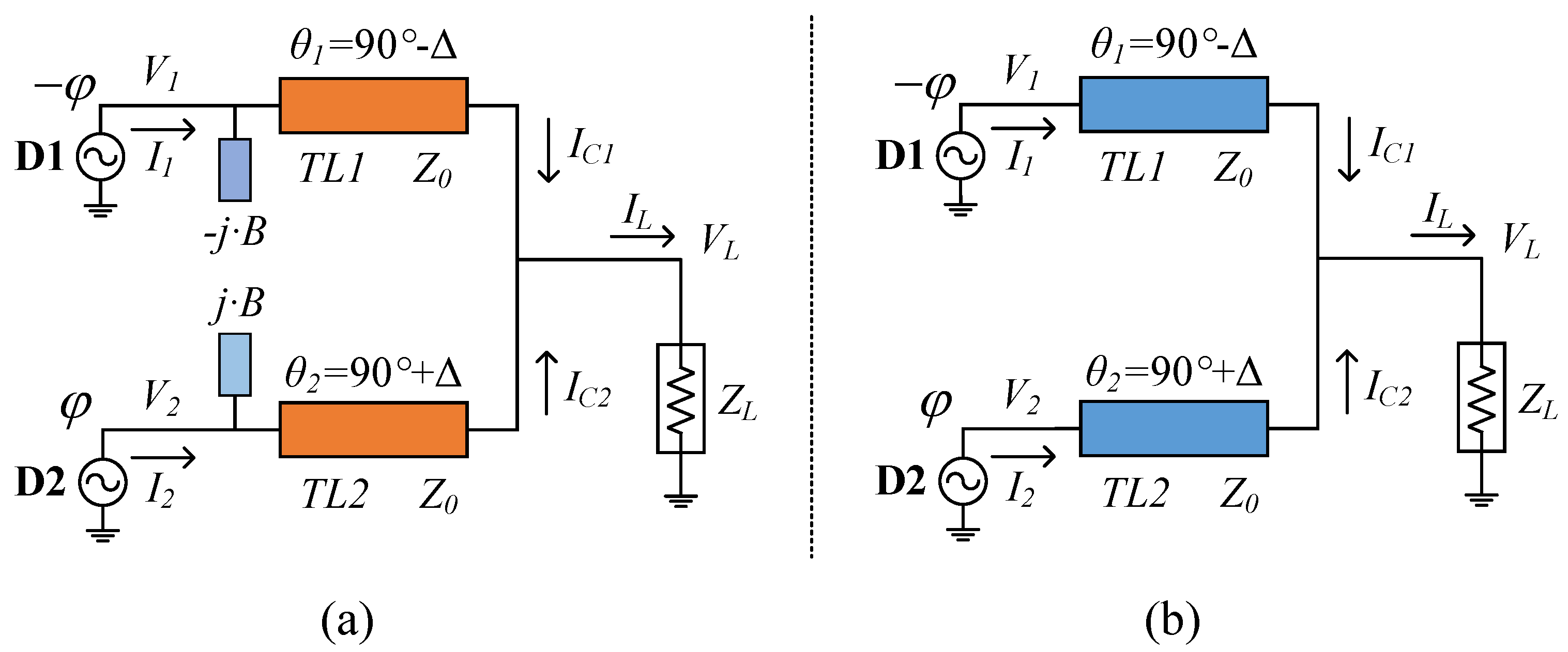
Outphasing power amplifiers (OPAs) are famous for their high-efficiency amplification leveraging on active load modulation [1]. A simplified block diagram of a classical OPA is shown in Figure 1. The high conversion efficiency of OPAs is achieved through phase modulation between two sub-amplifiers, which work in saturation conditions [2]. An efficient power amplifier (PA) solution can be adopted, such as class-E or class-F, by the two sub-amplifiers to boost the conversion efficiency [3,4,5,6]. Many studies have been conducted on OPAs, including circuit topology and design methods. For OPAs, the combiner plays a critical role for high-efficiency amplification [7,8]. Figure 2 shows two most popular combiners, the Chireix combiner and the non-commensurate transmission line (NCTL) combiner, for board-level OPA design.
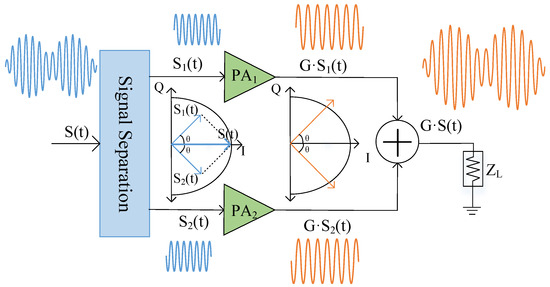
Figure 1.
Schematic block diagram of OPA.
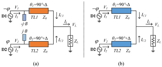
Figure 2.
Two most popular combiners for Outphasing PA, (a) Chireix combiner and (b) non-commensurate transmission line (NCTL) combiner for board-level OPA design.
In 1985, F. Raab conducted an analysis of the efficiency of an outphasing power amplifier (OPA) based on the Chireix combiner, revealing that the average efficiency of an OPA is determined by the shunt reactance [7]. This groundbreaking research demonstrated that optimal OPA efficiency can be achieved by selecting a shunt reactance that is precisely matched to the signal, thereby laying the theoretical foundation for subsequent advances in OPA design. Drawing on the principles established in Raab’s seminal work, several high-efficiency OPA implementations have been successfully realized, as documented in a series of subsequent studies [9,10,11,12,13]. In [12], El-Asmar proposed a simplified analysis method for the design of the Chireix OPA, which underscores the importance of precise control over the characteristic impedance and length of parallel TLs in maximizing the OPA’s average efficiency. In [13], an RF-input Chireix OPA working at 2.14 GHz was designed, maintaining a drain efficiency (DE) of more than 60% over a 5.5 dB output back-off (OBO) power range. This impressive feat underscores the practical significance of the theoretical insights and design methodologies that have been painstakingly developed and refined over the years, paving the way for continued innovation and advancement in the field of high-efficiency power amplification.
However, the above Chireix OPAs require the addition of two extra compensation components in parallel to ensure efficiency peaks at the power back-off point, which increases the complexity of the circuit topology [14,15,16]. To solve this problem, Gerhard proposed a new type of OPA combiner that eliminates the need for parallel reactance compensation components [14,15]. The new OPA combiner consists of two TLs with different electrical lengths [15], as shown in Figure 2b. The NCTL combiner can reduce circuit complexity and facilitate the practical implementation of OPAs. It has been demonstrated in many papers that the NCTL combiner has the same functions as the Chireix combiner [15,16,17]. In 2017, a 2.11 GHz RF-input OPA based on the NCTL combiner was successfully implemented and extensively analyzed, exhibiting a peak output power of 43.0 dBm coupled with a remarkable DE of 73% [17]. To further enhance the efficiency, a harmonic-tuned OPA based on the NCTL combiner was realized at 0.9 GHz in [6], achieving a power-added efficiency (PAE) of more than 60% over an OBO power range of 7 dB. These advancements in OPA technology have opened up new possibilities for high-efficiency power amplification in a wide range of applications, paving the way for more efficient and reliable wireless communication systems.
Notice that the two types of OPA combiner mentioned above can be applied to multi-way applications [18,19,20,21,22,23]. In 2014, a 2.14 GHz four-way Chireix OPA was meticulously designed [20], achieving a remarkable maximum output power of 62 W with an impressive drain efficiency (DE) of over 50% at an 8.4 dB output back-off (OBO). This underscores the effectiveness and scalability of the Chireix combiner approach in high-power amplification scenarios. Two years later, in 2016, a 2.14 GHz OPA leveraging the NCTL combiner approach was implemented [23]. This groundbreaking design demonstrated exceptional performance, delivering a saturation power of 105 W while maintaining a commendable DE of over 60% across a wide 6.2 dB OBO power range. This achievement underscores the potential of the NCTL combiner to enable highly efficient power amplification even in demanding multi-way configurations. These advancements offer valuable insights for the continued evolution of OPA technology, paving the way for future innovations in wireless communication systems that demand both high power and efficiency.
Though the above analysis shows that OPAs can achieve high efficiency over a large OBO power range, it is a challenge to design broadband or multi-band OPAs due to the frequency dispersion of the combiner [24,25]. Previous works have demonstrated that both the Chireix and NCTL combiners have limited bandwidth (typically less than 200 MHz). Therefore, it is interesting to conduct research on novel architectures and methods to design broadband and multi-band OPAs. Given these constraints, there is a compelling interest in exploring innovative architectures and methodologies to facilitate the design of broadband and multi-band OPAs. This paper presents an overview of recent advancements in this area, delving into the fundamental principles of OPA technology before delving into a comprehensive review of broadband OPA designs. Subsequently, a thorough examination of multi-band OPAs is presented, discussing their unique characteristics and challenges. Finally, this paper presents potential design strategies aimed at extending the frequency coverage of OPAs, thus paving the way for more versatile and adaptable power amplification solutions.
By addressing these critical research gaps, this work aims to contribute to the continued evolution of OPA technology, enabling more efficient and effective power amplification across a broader range of frequencies. This, in turn, holds profound implications for enhancing the performance and capabilities of wireless communication systems, driving forward technological innovation in this dynamic field.
2. Load Modulation of OPAs
This section will analyze the load modulation of OPAs based on the NCTL combiner, because it is the most useful combiner for designing board-level OPAs. Moreover, the bandwidth limitation of OPAs will be discussed. The NCTL combiner of an OPA consists of two TLs with electrical lengths of 90, as inllustrated in Figure 2b. The two sub-amplifiers of an OPA can be considered as two RF voltage sources and , which can be expressed as
where defines the phase modulation of the OPA.
Traditionally, the combining impedance is , as depicted in Figure 2b. Then, the load admittance of the two sub-amplifiers can be calculated as
Using the load admittance of the two sub-amplifiers, the efficiency of the OPA can be obtained as
Considering the frequency response of the OPA combiner, Equations (2)–(4) can be be re-calculated as
where
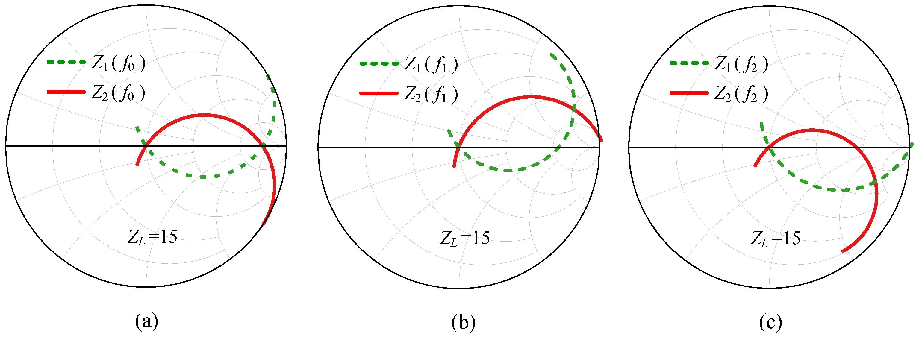
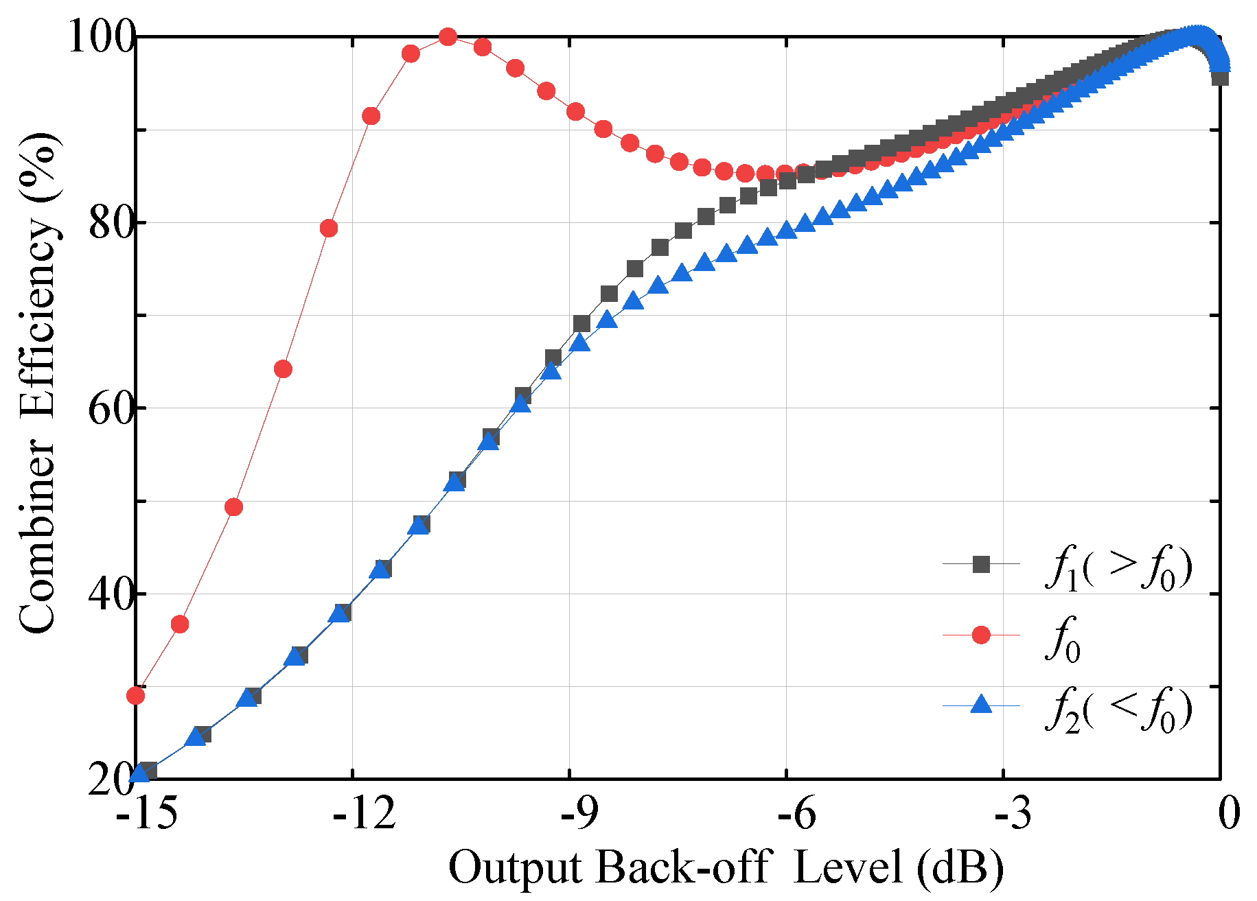
In (5)–(8), f is the normalized frequency, normalized to the center frequency. Using the above formulas, the load modulation trajectories of an OPA are shown in Figure 3 when . At the center frequency, , the two sub-amplifiers see a real load impedance at both back-off and saturation power levels, leading to an combined efficiency of 100%, as indicated in Figure 4 (the circled red line). However, as f deviates from one, the two sub-amplifiers will see a complex load impedance at the back-off power level, as shown in Figure 3b,c. When the working frequency goes higher, a positive imaginary part will be presented to the sub-amplifier of the OPA, as shown in Figure 3b, while a negative imaginary part will be presented to the sub-amplifier of the OPA when the frequency goes lower, as shown in Figure 3c. The reactive part of the load impedance presented to each sub-amplifier will decrease the combined efficiency, as shown in Figure 4. Therefore, the bandwidth of the OPA is limited by the frequency dispersion of the combiner.
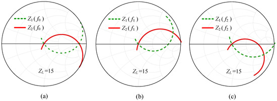
Figure 3.
Load modulation trajectories of an OPA at (a) , (b) at and (c) at when the combined impedance is .

Figure 4.
Efficiency of the NCTL combiner versus output power at different frequency points.
3. Review of Broadband OPAs
As illustrated in the above section, the combiner of an OPA limits its bandwidth. Therefore, it is interesting but challenging to address the bandwidth limitation of the OPA combiner. This section will review the state-of-the-art works for broadband OPA design [24,25,26,27]. In summary, there are three popular methods for extending the bandwidth of an OPA. These three methods can be named as broadband class-E OPA, broadband reconfigurable OPA and complex combined OPA. They will be discussed separately in the following parts.
3.1. Broadband Class-E OPAs
As a highly-efficient switch-mode power amplifier, class-E operation mode can be adopted by the sub-amplifier of an OPA to boost the conversion efficiency. To extend the bandwidth of an OPA, a fully analytical combiner design technique was developed for wideband class-E OPAs in [25]. The design parameters of the combiner network are firstly calculated based on the boundary conditions required for high-efficiency class-E PAs. Then, the bandwidth of the OPA is extended by introducing continuous mode operation into the synthesis approach. The load impedance required by the OPA for class-E operation can be calculated using
where n represents the harmonic index. Notice that the efficiency and output power are mainly affected by and [25]. The factor R can be derived based on the output power level:
According to the load modulation of the class-E PA, the design parameters of the OPA combiner can be derived. Based on the analytical combiner design method, a broadband class-E OPA was designed in [25], demonstrating that a DE of more than 71% can be obtained at saturation, and that more than 60% over a 6-dB OBO power range in the frequency band of 0.7–1.05 GHz can be obtained. Meanwhile, the fabricated broadband OPA in [25] was also simulated using a 5 MHz wideband signal. Simulation results showed that the broadband class-E OPA achieved an adjacent channel leakage ratio of better than −41 dBc with an average efficiency of more than 56% across the frequency band of interest.
3.2. Broadband Reconfigurable OPAs
Actually, the bandwidth of an OPA will be increased if optimal load modulation can be satisfied in a wide frequency band. To fulfill this requirement, tunable elements can be used in the OPA combiner to provide the OPA with optimal load modulation. This means a reconfigurable OPA has the potential to cover a wide bandwidth. In [27], a reconfigurable class-E OPA was proposed for broadband applications. To achieve optimum efficiency of the class-E OPA at different frequency bands, a single-ended class-E PA that achieved optimal operation under load modulation conditions was first analyzed. In [27], the losses of the switch were excluded for simplicity. The circuit can be described through a design set , where
These design sets are a function of the parameters q () and k, which is the slope of the switch voltage waveform across the output capacitor C at V. Then, the nominal load is derived using
In [27], the analytical solution was reported for the combination of q, k and the duty cycle d (= ). According to , we can satisfy q at a different operating frequency without modifying L or C but by simply changing the duty cycle. Notice that the reconfigurable technique in [27] can only be used in switch mode PAs and needs precise pulse width modulation. Meanwhile, the operating bandwidth of the OPA also depends on the duty cycle. In [27], a 1.8–2.2 GHz class-E OPA based on a frequency reconfigurable duty cycle was constructed and measured. The peak output power was 42 dBm and varied +/− O.3 dB across the three frequency bands. The broadband class-E OPA exhibited a 6 dB back-off DE of more than 60% in the frequency band of 1.8–2.2 GHz.
3.3. Complex Combining Impedance for Broadband Applications
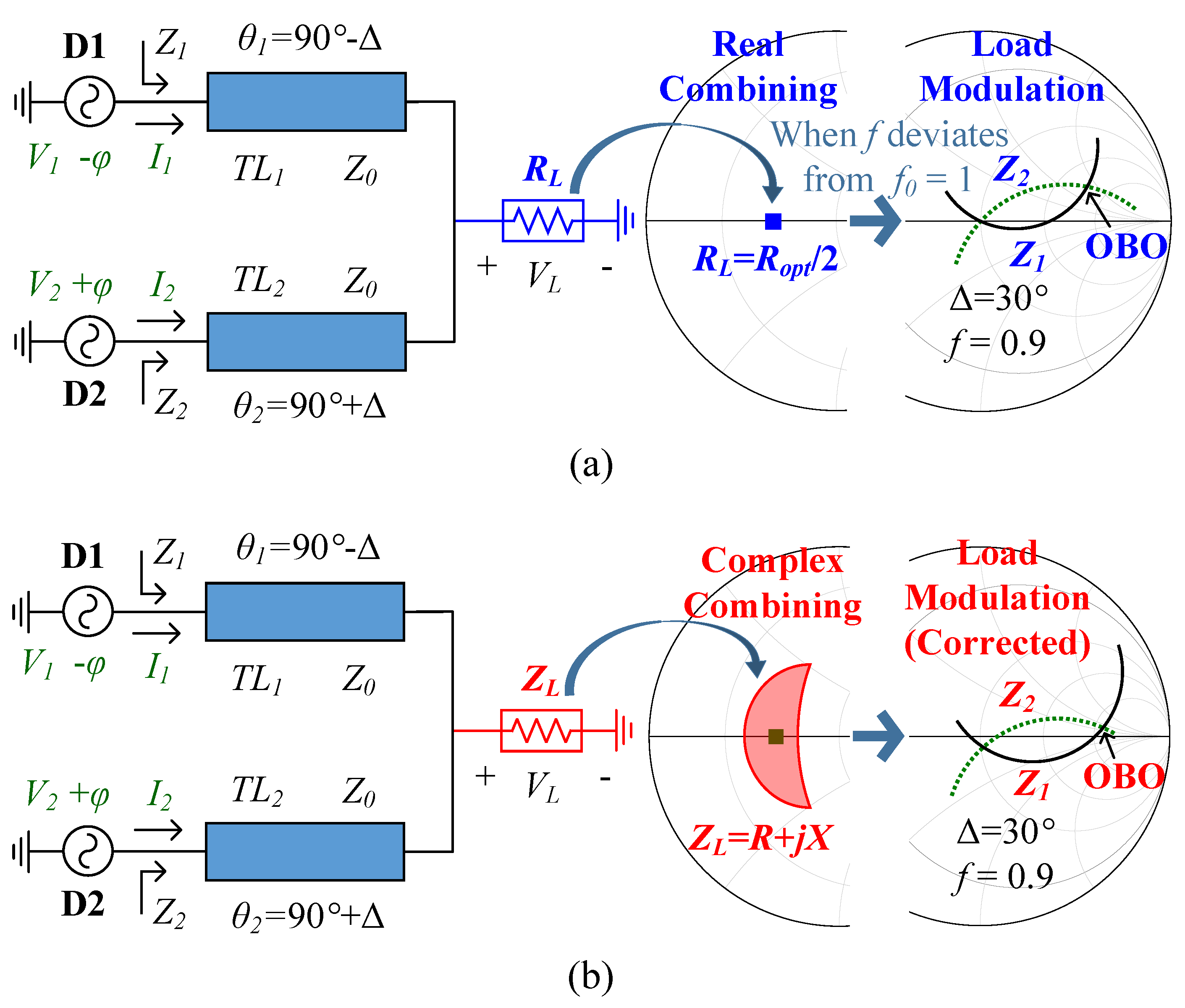
Unlike the above works, a novel design methodology was proposed in [28] to extend the bandwidth of an NCTL-based OPA. As shown in Figure 5a, the frequency dispersion of the NCTL combiner limited the bandwidth of the OPA. To overcome this problem, a complex combining method was proposed, as shown in Figure 5b. Complex combining impedance can be used to compensate the reactive part presented to each sub-amplifier when the working frequency deviates from the center point. In this way, the two sub-amplifiers will see an almost purely real load impedance at the back-off power level, as shown in Figure 5b.
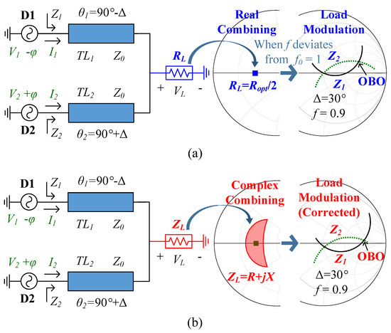
Figure 5.
Simplified block diagram and combining methods of (a) the traditional NCTL-based OPA and (b) the complex combined OPA.
From (5) and (6), the load impedance of each sub-amplifier in the OPA is a function of the combining load . To make sure each sub-amplifier sees a real load impedance at the back-off power level, the following equation should be satisfied:
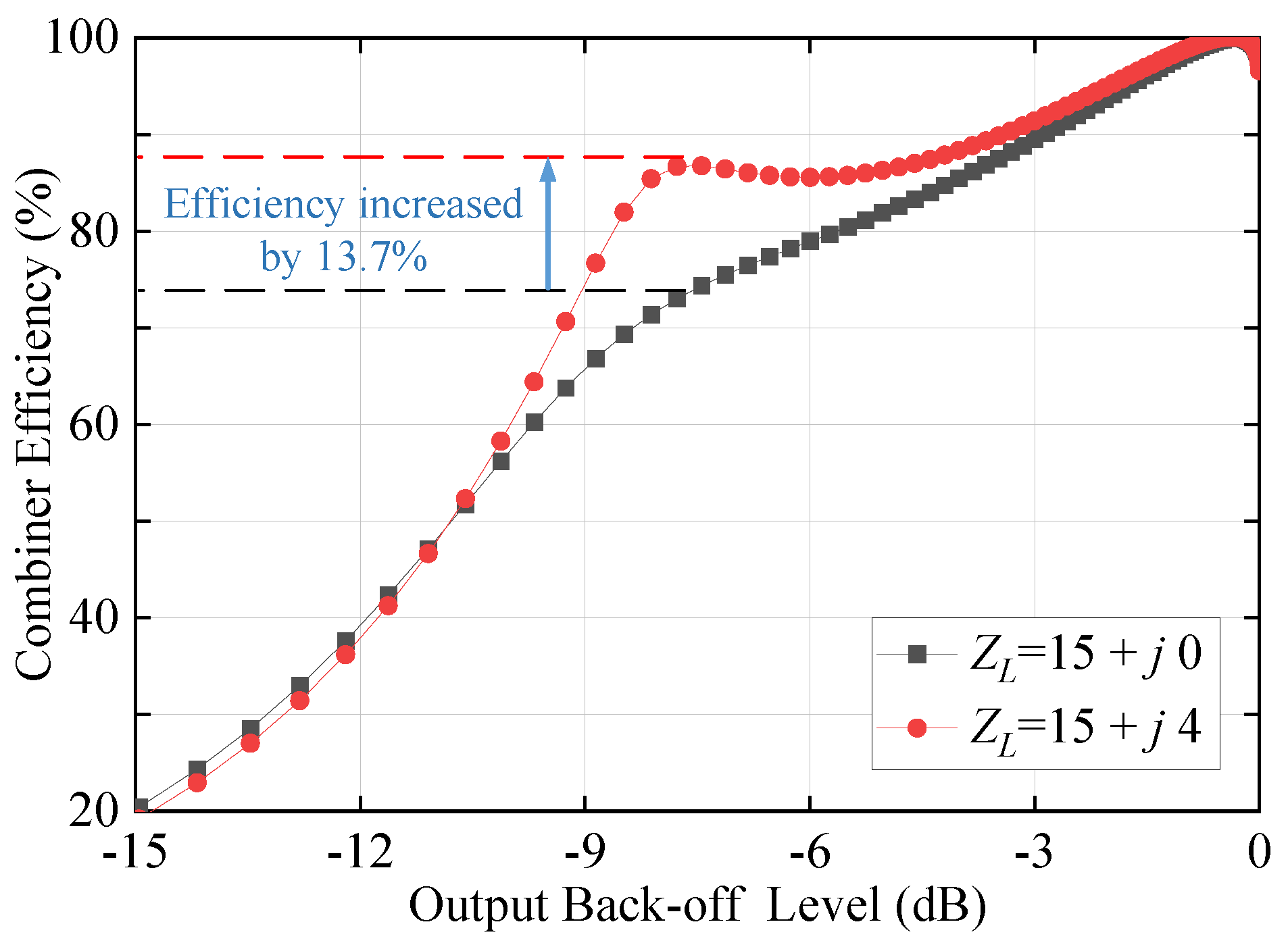
This equation means the reactive part of the load impedance presented to each sub-amplifier can be compensated by a specific . After compensating the reactive part, the efficiency of the OPA will be recovered. Figure 6 compares the combining efficiency of an OPA at f = 0.9 when . Compared to the real combining method, the OPA efficiency can be increased by 13.7% by using the complex combining method. Most importantly, the complex combined OPA does not need any tunable elements in the combiner. This will reduce extra power losses.
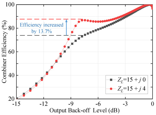
Figure 6.
Calculated efficiencies of the NCTL combiner when f = 0.9.
To demonstrate the complex combining method, a high-efficiency broadband OPA operating at 1.7–2.2 GHz frequency band was implemented and measured in [28]. The measured saturation power and DE of the broadband OPA are 43.1–44.3 dBm and 63.4–78.4%, respectively. At the same time, a DE of 45.4–70.4% can also be obtained at the 6 dB OBO power level.
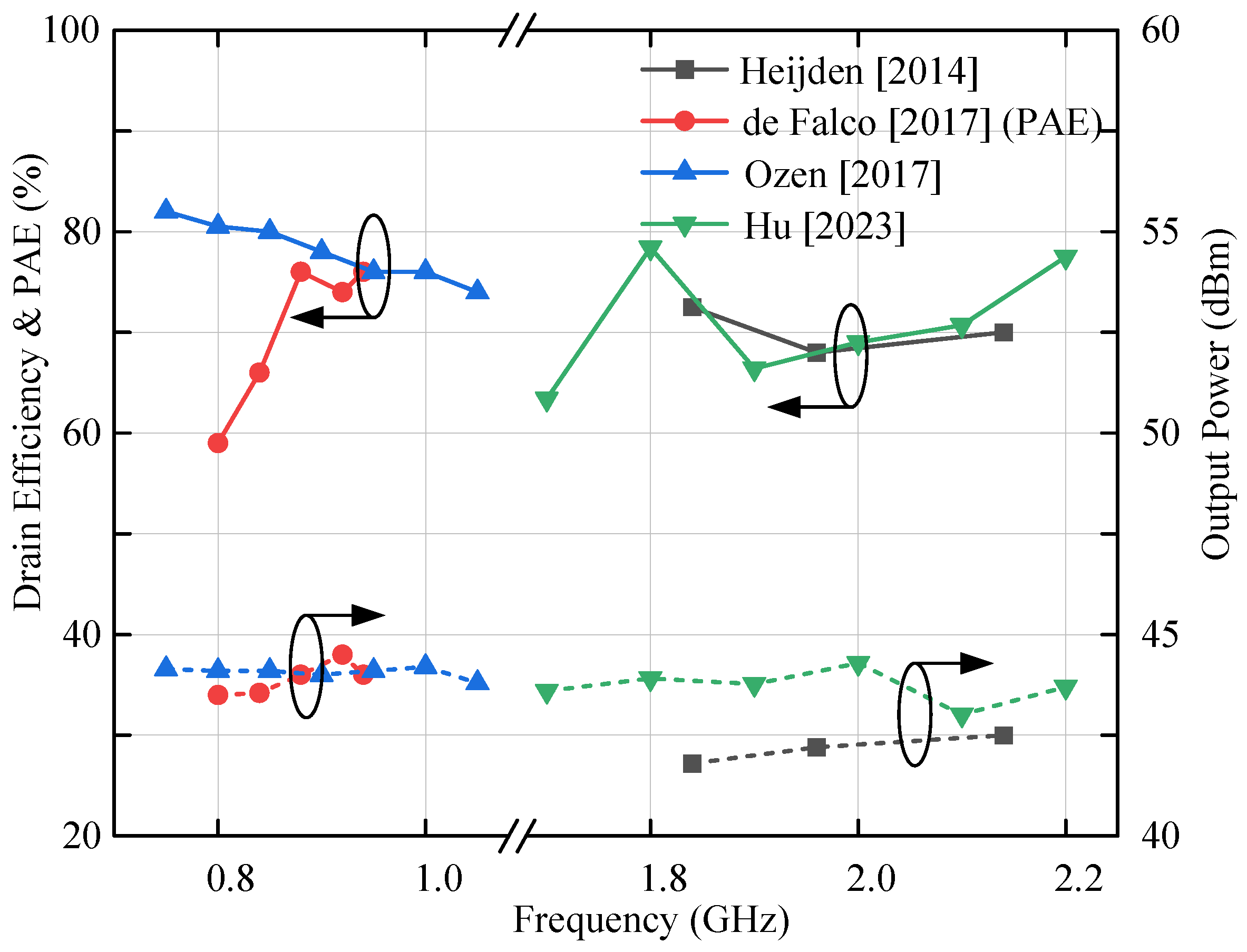
To compare broadband high-efficiency OPAs, the performances of the recent published broadband OPAs are listed in Table 1. Correspondingly, the DE (or PAE) and output power of the broadband OPAs versus the working frequency are shown in Figure 7.

Table 1.
Performance comparison of recently published broadband OPAs.
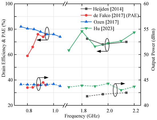
Figure 7.
Drain efficiency (or PAE) and output power of recently published broadband OPAs versus the working frequency in Table 1 [6,25,27,28].
4. Review of Multi-Band OPAs
The above section shows some advanced techniques to extend an OPA’s bandwidth. However, it is still hard for an OPA to maintain high efficiency when the fractional bandwidth exceeds 30%, as shown in Figure 7. To further extend the frequency coverage of an OPA, multi-band operation is a good candidate. Until now, only a few articles have carried out research on multi-band OPAs [29,30,31,32,33,34]. Furthermore, the design methods in these articles can be divided into three categories: the reconfigurable technique based on tunable elements, multi-band matching topology based on the T or network and the multi-mode operation-based frequency periodicity of TLs.
4.1. Reconfigurable OPAs for Multi-Band Applications
The reconfigurable technique can be used not only to extend the bandwidth of an OPA but also to design multi-band OPAs. The load modulation trajectory of an OPA at different frequencies can be optimized by tunable elements, leading to multi-band operation. In [30], a tri-band OPA operating at 1.65, 2.1 and 2.35 GHz was realized by integrating a tunable capacitor and inductor into the Chireix combiner. The tunable capacitor and inductor were designed using varactor diode SMV1430 from SKYWORK. To support the high-voltage swing of the output signal, three varactor diodes with serial back-to-back connection were adopted by both the capacitor and inductor. In [30], the tri-band OPA obtained a DE of more than 40% over a 5–6 dB OBO power range at the targeted three frequency points.
4.2. Multi-Band Matching Topology for Multi-Band OPAs
It has been demonstrated by many multi-band PAs that T- and -type matching networks can be used to realize multi-band matching. Therefore, these multi-band matching topologies can be adopted by OPAs to enable multi-band operation. In [31,32], 2.6/3.5 GHz dual-band OPAs were realized based on the multi-band matching topology.
In [31], a dual-band Chireix OPA was realized using T-type matching topology. The input matching network (IMN), impedance inverter and the reactance compensation network were all realized based on T-type matching topology. A comprehensive theoretical formulation for calculating the parameters of the T-type matching topology was also given in [31]. The fabricated dual-band OPA in [31] achieved saturation DEs of 71% and 64% at 2.6 and 3.5 GHz, respectively. Meanwhile, 6 dB back-off DEs of 58.4% and 50.1% were also measured at 2.6 and 3.5 GHz.
In [32], a 2.6/3.5 GHz dual-band OPA was designed based on a dual-band NCTL combiner, which was realized using stub-loaded transmission lines (SLTLs). Each sub-amplifier in the dual-band OPA adopted a broadband IMN. The SLTL in the NCTL combiner was constructed by integrating two T-type networks into a -type network. The circuit parameters of the SLTL after each sub-amplifier were calculated leveraging the -metric theory. Based on the schematic shown in [32], a dual-band OPA was simulated, fabricated and measured, exhibiting excellent performances. At 2.6 GHz, the measured average output power was 37.3 dBm and a DE of 51.2% can be achieved, respectively. At 3.5 GHz, the measured output power and efficiency were 36.9 dBm and 40.6%, respectively.
4.3. Multi-Mode Multi-Band OPAs Based on Frequency Periodicity
Normally, the phase delay of a passive network is periodic. It has been demonstrated that the frequency periodicity of a transmission line can be utilized to design multi-mode PAs that cover an ultra-wideband area, such as the PAs in [24,35]. The frequency periodicity can also be adopted when designing multi-band OPAs, especially NCTL-based OPAs.
In [33], the authors demonstrated that the OPA could obtain correct load modulation by adding an additional half-wavelength transmission line to one of the branches in the NCTL combiner. It was validated in [33] that the three NCTL combiners are all suitable for OPA design. From [33], the phase delay of the transmission lines in the combiners are different. Meanwhile, for a fixed NCTL combiner, it has different electrical behaviors at different frequencies. Therefore, dual-band operation can be obtained if an NCTL combiner conforms to one of the three combiners at two different frequency points. Based on this theory, a dual-band OPA working at 2.6 and 3.5 GHz was implemented and measured in [33]. The dual-band OPA in [33] achieve maximum output powers of 44.4 and 44.3 dBm with DEs of 69.5% and 69.2% at 2.6 and 3.5 GHz, respectively. Meanwhile, 6 dB back-off DEs of 62.4% and 63.5% were also obtained by the dual-band OPA at 2.6 and 3.5 GHz, respectively.
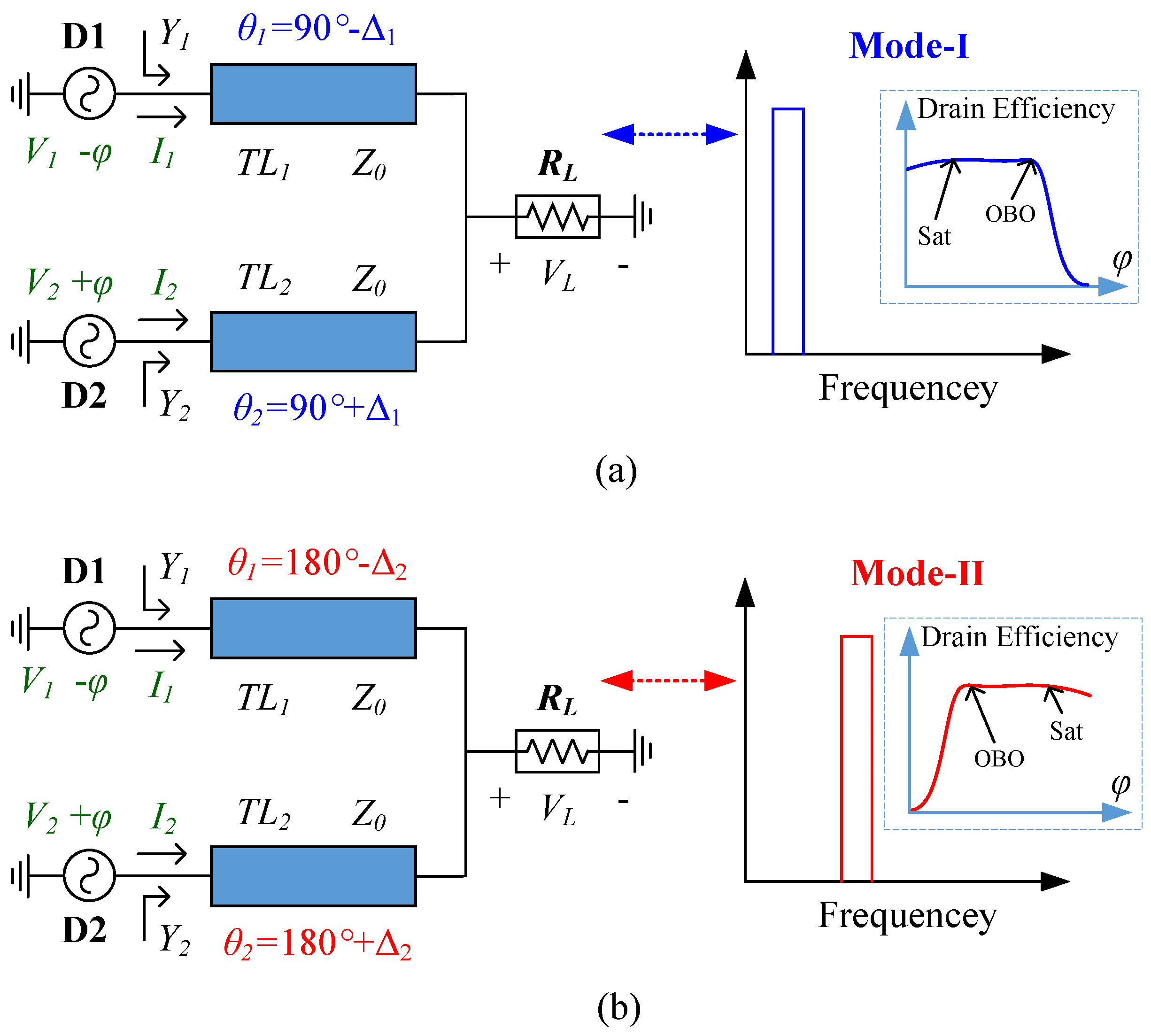
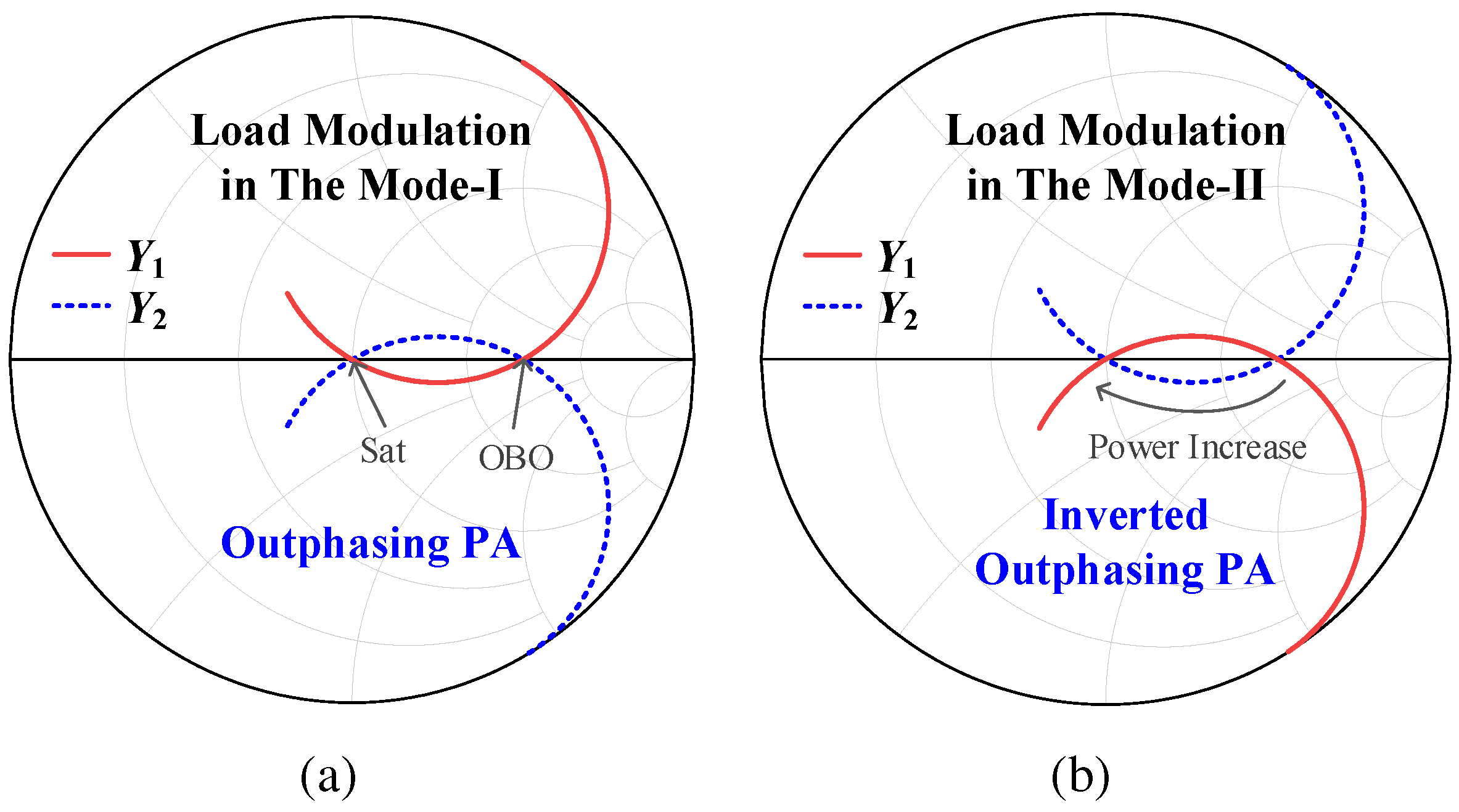
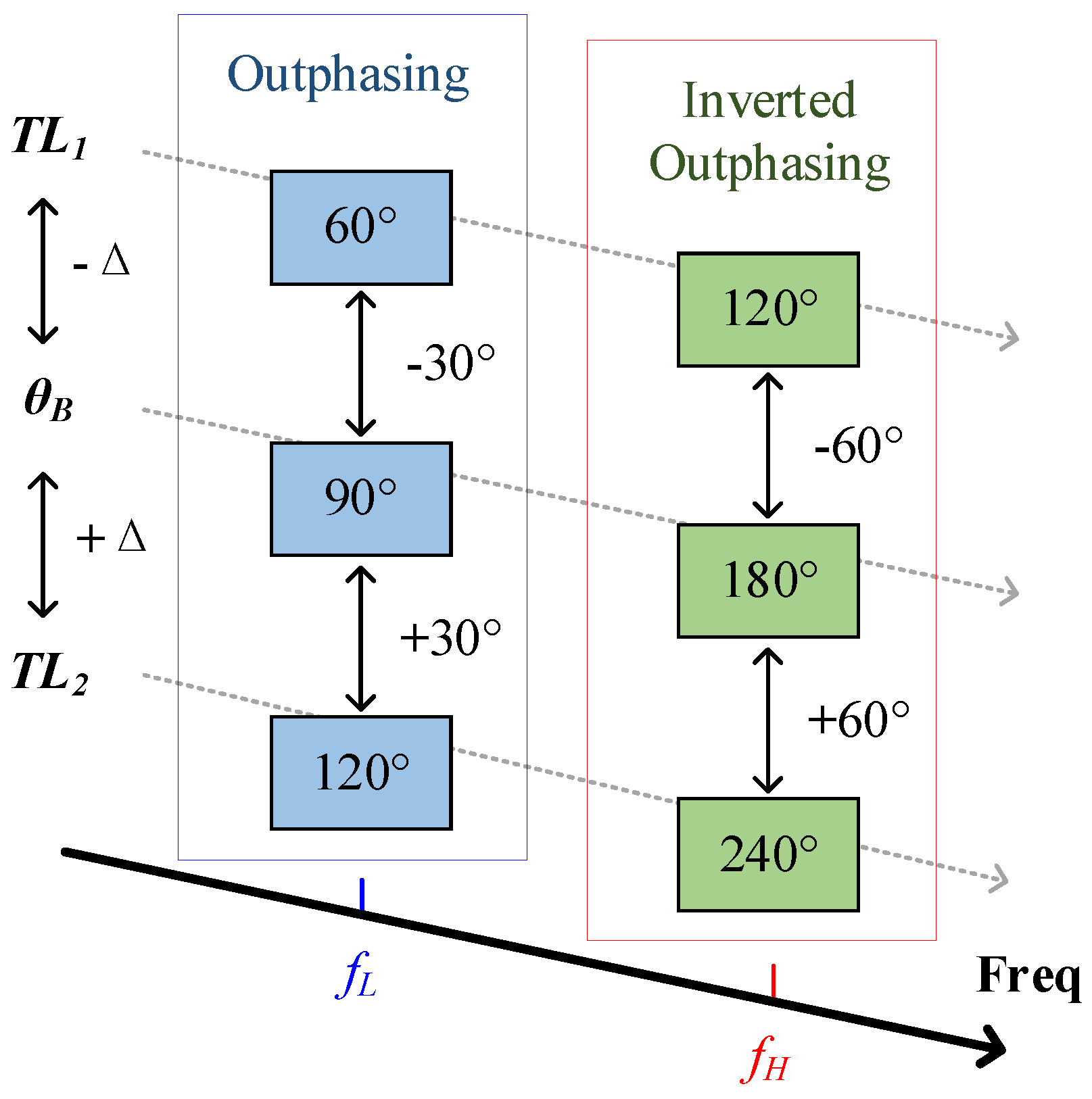
As shown in [33], the base length of transmission lines in the NCTL combiner is 90. Indeed, there are two solutions of base length that can be used to construct OPAs. One is 90 and the other is 180, as shown in Figure 8a,b. Meanwhile, the delta length ( and in Figure 8) should be different. In [34], the authors defined these two solutions as Mode-I and Mode-II, respectively. According to the theoretical analysis in [34], the load modulation trajectories of these two operation modes are opposite to each other, as shown in Figure 9. Therefore, the OPAs operating in Mode-I and Mode-II are, respectively, named OPA and inverted OPA (IOPA). To enable a 6 dB OBO power level in each operation mode, and should be simultaneously satisfied. Figure 10 shows the phase delay requirements of the OPA and IOPA. Notice that the phase delay of the transmission lines in the IOPA combiner is twice that in the OPA combiner. As we all know, the phase delay of a transmission line changes linearly versus by frequency. Therefore, a dual-band OPA can be obtained if the higher frequency is two times the lower frequency ().
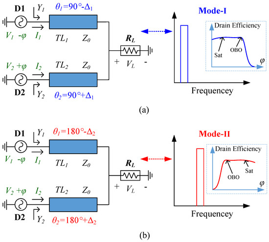
Figure 8.
Block diagrams of the dual-mode OPA when it operates in (a) Mode-I and (b) Mode-II in [34].

Figure 9.
Load modulation trajectories of the (a) OPA and (b) IOPA.
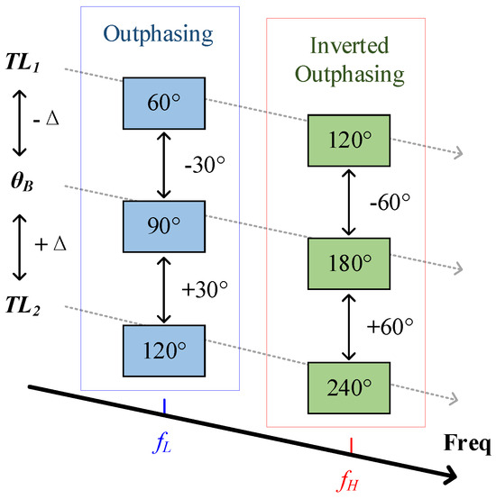
Figure 10.
Phase delay requirements of the OPA and IOPA.
A dual-band OPA was realized in [34] to verify the dual-mode theory. The operation frequencies were set to 1 and 2 GHz (two times), respectively. The OPA delivered a maximum output power of 42.8–43 dBm, a saturation DE of 58.4–62.5%, a saturation gain of 9.7–10.1 dB and a 6 dB back-off DE of 41.3–46.2% over 0.89–0.93 GHz (40 MHz) in Mode-I. On the other hand, when the OPA was in Mode-II, it achieved a maximum output power of 43.7–44.3 dBm, a saturation DE of 50.6–57.7%, a saturation gain of 10.8–11.5 dB and a 6 dB back-off DE of 50.1–62.3% over 1.89–1.96 GHz (70 MHz).
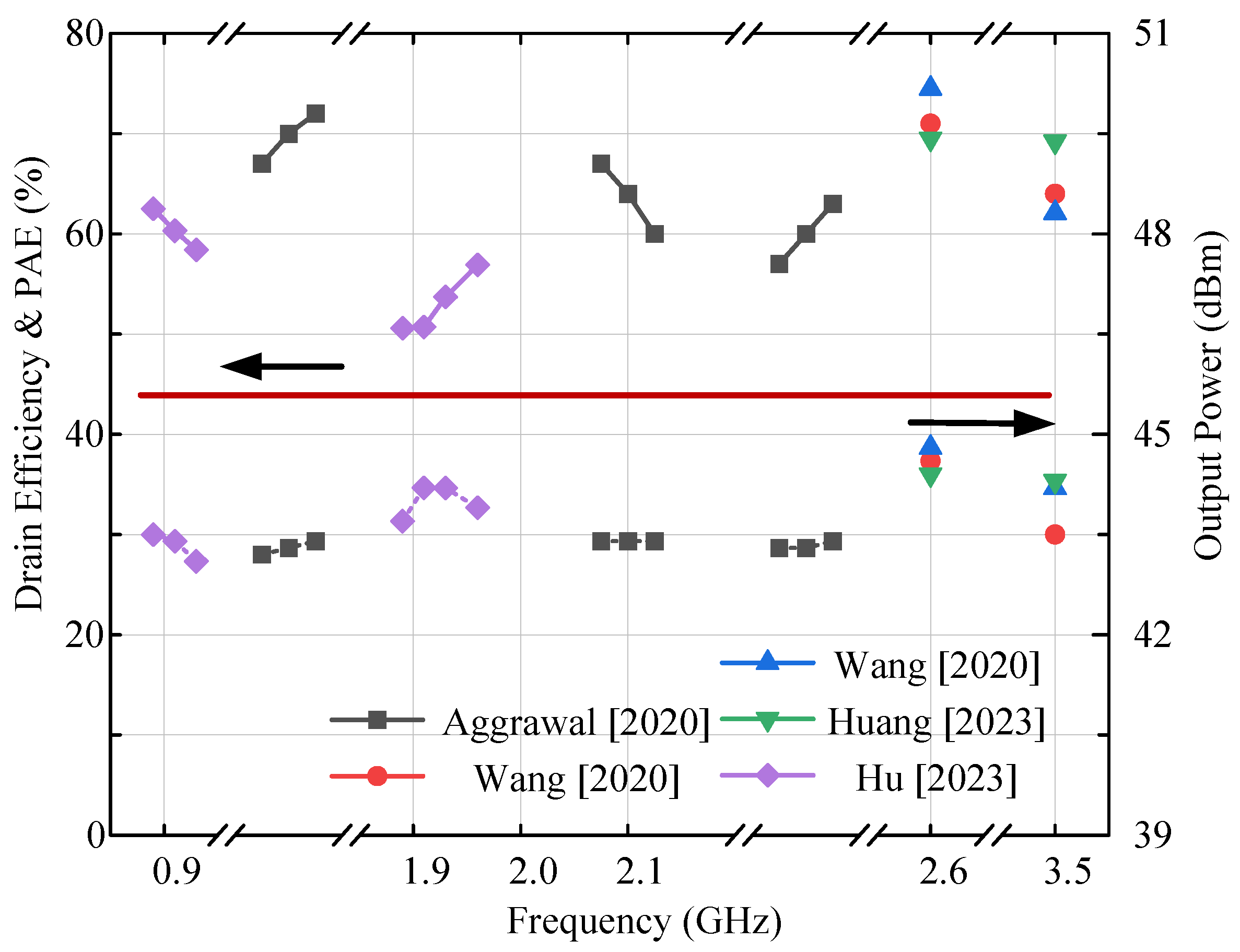
For comparison, the measurement results of state-of-the-art dual-band OPAs are listed in Table 2. Similarly, the drain efficiency and output power of the recently published multi-band OPAs versus the working frequency are shown in Figure 11.

Table 2.
Measurement results and performance comparison of recently published multi-band OPAs.
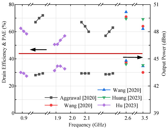
Figure 11.
Drain efficiency and output power of the recently published multi-band OPA versus the working frequency in Table 2, where the arrow represents the direction of the reference Y-axis [30,31,32,33,34].
5. Potential Solutions for Broadband and Multi-Band OPAs
The above two sections presented some progress of broadband and multi-band OPAs. Though there exist some promising design methods, more advanced techniques are still required to further improve the frequency coverage of OPAs. Based on previous research, the reconfigurable technique based on tunable elements is a popular method to design broadband and multi-band OPAs. However, the tunable elements will complicate the OPA design and cause additional power loss. In view of the above, the complex combining method proposed in [25] and the analytical combiner design technique proposed in [28] are two potential solutions to design broadband OPAs. For multi-band OPAs, two operation modes based on the periodicity of the transmission line were explored in [34]. Indeed, more operation modes of the OPA can be further enriched by considering the frequency periodicity of the NCTL combiner. Therefore, to achieve multi-band OPAs, one potential solution is to fully utilize the periodicity of the NCTL combiner. On the other hand, the digital control technique could provide flexible input signal splitting [36,37,38,39,40]. For traditional OPAs, the problem of high system complexity limits their application to some extent. With the development of the digital control technique, its introduction into the OPA system can effectively solve this problem. Through the optimization of the digital front end, the efficiency and output power of OPAs can be maximized.
Another noteworthy point is that the efficiency and linearity of OPAs are highly related to the symmetry of their two sub-amplifiers. It is very difficult to design a fully symmetrical sub-amplifier, especially for wideband operation. To realize symmetrical sub-amplifiers in an OPA, accuracy models are required by both the active and passive elements. Therefore, it is valuable to conduct research on the modeling of the transistors and passive elements, especially in integrated systems.
6. Conclusions
This paper gives a comprehensive review of the development of broadband and multi-band OPAs for high-efficiency amplification. The OPA load modulation is studied based on an NCTL combiner. Furthermore, the bandwidth limitation of OPAs is discussed. Some promising methods for extending the bandwidth of OPAs are presented, including the analytical combiner synthesis technique, the reconfigurable technique and the complex combining technique. Subsequently, the design methods for multi-band OPAs are discussed. Finally, the potential design methods for broadband and multi-band OPAs are pointed out. In summary, this paper systematically summarizes the development of broadband and multi-band OPAs for high-efficiency amplification. These research findings provide valuable references for the design and application of high-efficiency PAs and offer direction and inspiration for future research. Based on the review in this paper, the design theories of broadband and multi-band OPAs are far from mature. Therefore, there are many aspects worth studying to improve the performances of OPAs.
Author Contributions
Writing—original draft preparation, Y.Z., C.H. and X.L.; writing—review and editing, J.W., W.Z., P.T. and S.L.; supervision, W.S. All authors have read and agreed to the published version of the manuscript.
Funding
This research was funded by the National Natural Science Foundation of China, grant numbers 62201100, 62171065, 62171068 and 62001061, and by the Basic Research Funds for Central Universities, grant number 2022CDJJMRH-010.
Data Availability Statement
The data in this review are all from references.
Conflicts of Interest
The authors declare no conflict of interest.
References
- Chireix, H. High power outphasing modulation. Proc. Inst. Radio Eng. 1935, 11, 1370–1392. [Google Scholar] [CrossRef]
- Barton, T. Not just a phase: Outphasing power amplifiers. IEEE Microw. Mag. 2016, 2, 18–31. [Google Scholar] [CrossRef]
- Ghahremani, A.; Annema, A.; Nauta, B. Outphasing class-E power amplifiers: From theory to back-off efficiency improvement. IEEE J. Solid-State Circuits 2018, 5, 1374–1386. [Google Scholar] [CrossRef]
- Afanasyev, P.; Grebennikov, A.; Farrell, R.; Dooley, J. Analysis and design of Outphasing transmitter using class-E power amplifiers with shunt capacitances and shunt filters. IEEE Access 2020, 8, 208879–208891. [Google Scholar] [CrossRef]
- Hwang, T.; Azadet, K.; Wilson, R.S.; Lin, J. Characterization of class-F power amplifier with wide amplitude and phase bandwidth for Outphasing architecture. IEEE Microw. Wireless Compon. Lett. 2014, 3, 188–190. [Google Scholar] [CrossRef]
- de Falco, P.E.; Pednekar, P.; Mimis, K.; Smida, S.B.; Watkins, G.; Morris, K.; Barton, T.W. Load modulation of harmonically tuned amplifiers and application to Outphasing systems. IEEE Trans. Microw. Theory Tech. 2017, 10, 3596–3612. [Google Scholar] [CrossRef]
- Raab, F.H. Efficiency of outphasing RF power-amplifier systems. IEEE Trans. Commun. 1985, 10, 1094–1099. [Google Scholar] [CrossRef]
- Litchfield, M.; Cappello, T. The various angles of Outphasing PAs: Competitiveness of Outphasing in efficient linear PA applications. IEEE Microw. Mag. 2019, 4, 135–145. [Google Scholar] [CrossRef]
- Birafane, A.; Kouki, A.B. On the linearity and efficiency of outphasing microwave amplifiers. IEEE Trans. Microw. Theory Tech. 2004, 7, 1702–1708. [Google Scholar] [CrossRef]
- Hakala, I.; Choi, D.K.; Gharavi, L.; Kajakine, N.; Koskela, J.; Kaunisto, R. A 2.14-GHz Chireix outphasing transmitter. IEEE Trans. Microw. Theory Tech. 2005, 6, 2129–2138. [Google Scholar] [CrossRef]
- Eun, S.-K.; Ji, S.H.; Cho, C.S.; Lee, J.W.; Kim, J. A high linearity Chireix outphasing power amplifier using composite right/left-handed transmission lines. In Proceedings of the 2007 European Microwave Conference, Munich, Germany, 10–12 October 2007; pp. 1622–1625. [Google Scholar]
- El-Asmar, M.; Birafane, A.; Helaoui, M.; Kouki, A.B.; Ghannouchi, F.M. Analytical design methodology of Outphasing amplification systems using a new simplified Chireix combiner model. IEEE Trans. Microw. Theory Tech. 2012, 6, 1886–1895. [Google Scholar] [CrossRef]
- Faraji, N.; Barton, T.W. An RF-input chireix outphasing power amplifier. In Proceedings of the 2016 IEEE Topical Conference on Power Amplifiers for Wireless and Radio Applications (PAWR), Austin, TX, USA, 24–27 January 2016; pp. 11–14. [Google Scholar]
- Gerhard, W.; Knoechel, R. Novel transmission line combiner for highly efficient Outphasing RF power amplifiers. In Proceedings of the 37th European Microwave Conference, Munich, Germany, 9–12 October 2007; pp. 1433–1436. [Google Scholar]
- Gerhard, W.; Knoechel, R. Improved design of outphasing power amplifier combiners. In Proceedings of the 2009 German Microwave Conference, Munich, Germany, 16–18 March 2009; pp. 1–4. [Google Scholar]
- Jang, H.; Wilson, R.; Canning, T.; Seebacher, D.; Schuberth, C.; Arigong, B.; Trang, F.; Ward, S. RF-input self-outphasing Doherty–Chireix combined amplifier. IEEE Trans. Microw. Theory Tech. 2016, 12, 4518–4534. [Google Scholar] [CrossRef]
- Nguyen, H.Q.; Barton, T.W. Linearity Characterization of RF-input Chireix Outphasing Power Amplifier. In Proceedings of the IInd General Assembly and Scientific Symposium of the International Union of Radio Science (URSI GASS), Montreal, QC, Canada, 19–26 August 2017; pp. 1–4. [Google Scholar]
- Perreault, D.J. A new power combining and outphasing modulation system for high-efficiency power amplification. IEEE Trans. Circuits Syst. I Reg. Pap. 2011, 8, 1713–1726. [Google Scholar] [CrossRef]
- Barton, T.W.; Dawson, J.L.; Perreault, D.J. Four-way lossless outphasing and power combining with hybrid microstrip/discrete combiner for microwave power amplification. In Proceedings of the 2013 IEEE MTT-S International Microwave Symposium Digest (MTT), Seattle, WA, USA, 2–7 June 2013; pp. 1–4. [Google Scholar]
- Barton, T.W.; Perreault, D.J. Four-way microstrip-based power combining for microwave Outphasing power amplifiers. IEEE Trans. Circuits Syst. Regul. Pap. 2014, 10, 2987–2998. [Google Scholar] [CrossRef]
- Barton, T.W.; Jurkov, A.S.; Perreault, D.J. Transmission-line based multi-way lossless power combining and outphasing system. In Proceedings of the 2014 IEEE MTT-S International Microwave Symposium (IMS2014), Tampa, FL, USA, 1–6 June 2014; pp. 1–4. [Google Scholar]
- Barton, T.W.; Perreault, D.J. Theory and implementation of RF-input outphasing power amplification. IEEE Trans. Microw. Theory Tech. 2015, 12, 4273–4283. [Google Scholar] [CrossRef]
- Barton, T.W.; Jurkov, A.S.; Pednekar, P.H.; Perreault, D.J. Multi-Way Lossless Outphasing System Based on an All-Transmission-Line Combiner. IEEE Trans. Microw. Theory Tech. 2016, 4, 1313–1326. [Google Scholar] [CrossRef]
- Komatsuzaki, Y.; Ma, R.; Benosman, M.; Nagai, Y.; Sakata, S.; Nakatani, K.; Shinjo, S. A Novel 1.4–4.8 GHz ultra-wideband, over 45% high efficiency digitally assisted frequency-periodic load modulated amplifier. In Proceedings of the 2019 IEEE MTT-S International Microwave Symposium (IMS), Boston, MA, USA, 2–7 June 2019; pp. 706–709. [Google Scholar]
- Ozen, M.; Heijden, M.; Acar, M.; Jos, R.; Fager, C. A generalized combiner synthesis technique for class-E outphasing transmitters. IEEE Trans. Circuits Syst. Reg. Pap. 2017, 5, 1126–1139. [Google Scholar] [CrossRef]
- Holzer, K.D.; Yuan, W.; Walling, J.S. Wideband techniques for Outphasing power amplifiers. IEEE Trans. Circuits Syst. Reg. Pap. 2018, 9, 2715–2725. [Google Scholar] [CrossRef]
- Heijden, M.; Acar, M. A radio-frequency reconfigurable CMOS-GaN class-E Chireix power amplifier. In Proceedings of the IEEE MTT-S International Microwave Symposium, Tampa, FL, USA, 1–6 June 2014; pp. 1–4. [Google Scholar]
- Hu, C.; Yang, R.; Shi, W.; Li, L.; Gao, R.; Dai, Z.; Pang, J.; Li, M. Analysis and design of broadband Outphasing power amplifier based on complex combining impedance. IEEE Trans. Circuits Syst. Reg. Pap. 2023, 4, 1542–1554. [Google Scholar] [CrossRef]
- Ruiz, M.N.; Morante, R.; Rizo, L.; García, J.A.; Gilabert, P.L.; Montoro, G. A dual-band outphasing transmitter using broadband class-E power amplifiers. In Proceedings of the 2014 International Workshop on Integrated Nonlinear Microwave and Millimetre-Wave Circuits (INMMiC), Leuven, Belgium, 2–4 April 2014; pp. 1–3. [Google Scholar]
- Aggrawal, E.; Rawat, K. Reconfigurable Chireix Outphasing power amplifier over multiple frequency bands. IEEE Trans. Circuits Syst. II Express Briefs 2020, 6, 1019–1023. [Google Scholar] [CrossRef]
- Wang, W.; Chen, S.; Cai, J.; Zhou, X.; Chan, W.S.; Wang, G. A high efficiency dual-band outphasing power amplifier design. Int. J. Microw. Comput. Eng. 2021, 31, e22515. [Google Scholar]
- Wang, W.; Chen, S.; Cai, J.; Zhou, X.; Chan, W.S.; Wang, G.; Xue, Q. A dual-band Outphasing power amplifier based on noncommensurate transmission line concept. IEEE Trans. Microw. Theory Tech. 2020, 7, 3079–3089. [Google Scholar] [CrossRef]
- Huang, J.; Chen, S.; Cai, J.; Xu, K.; Wang, G.; Zhou, X. A dual-band Outphaisng power amplifier based on multi-topology fitting. In Proceedings of the 2023 IEEE MTT-S International Wireless Symposium (IWS), Qingdao, China, 14–17 May 2023; pp. 1–3. [Google Scholar]
- Hu, C.; Shi, W.; Yang, R.; Lin, S.; Dai, Z.; Pang, J.; Li, M. Design of dual-mode dual-band Outphasing power amplifier leveraging on periodicity of non-commensurate transmission line combiner. IEEE Trans. Circuits Syst. II Express Briefs 2023, 70, 4384–4388. [Google Scholar] [CrossRef]
- Andersson, C.; Gustafsson, D.; Cahuana, J.C.; Hellberg, R.; Fager, C. A 1–3-GHz digitally controlled dual-RF input power-amplifier design based on a Doherty-outphasing continuum analysis. IEEE Trans. Microw. Theory Tech. 2013, 10, 3743–3752. [Google Scholar] [CrossRef]
- Kantana, C.; Benosman, M.; Ma, R.; Komatsuzaki, Y. A System Approach for Efficiency Enhancement and Linearization Technique of Dual-Input Doherty Power Amplifier. IEEE J. Microw. 2023, 3, 115–133. [Google Scholar] [CrossRef]
- Mengozzi, M.; Gibiino, G.P.; Angelotti, A.M.; Santarelli, A.; Florian, C.; Colantonio, P. Automatic Optimization of Input Split and Bias Voltage in Digitally Controlled Dual-Input Doherty RF PAs. Energies 2022, 15, 4892. [Google Scholar] [CrossRef]
- Barthwal, A.; Rawat, K.; Koul, S.K. Dual Input Digitally Controlled Broadband Three-Stage Doherty Power Amplifier with Back-off Reconfigurability. IEEE Trans. Circuits Syst. Regul. Pap. 2021, 68, 1421–1431. [Google Scholar] [CrossRef]
- Shi, W.; He, S.; Peng, J.; Wang, J. Digital Dual-Input Doherty Configuration for Ultrawideband Application. IEEE Trans. Ind. Electron. 2020, 67, 7509–7518. [Google Scholar] [CrossRef]
- Kalyan, R.; Rawat, K.; Koul, S.K. A Digitally Assisted Dual-Input Dual-Band Doherty Power Amplifier With Enhanced Efficiency and Linearity. IEEE Trans. Circuits Syst. Express Briefs 2019, 66, 297–301. [Google Scholar] [CrossRef]
Disclaimer/Publisher’s Note: The statements, opinions and data contained in all publications are solely those of the individual author(s) and contributor(s) and not of MDPI and/or the editor(s). MDPI and/or the editor(s) disclaim responsibility for any injury to people or property resulting from any ideas, methods, instructions or products referred to in the content. |
© 2023 by the authors. Licensee MDPI, Basel, Switzerland. This article is an open access article distributed under the terms and conditions of the Creative Commons Attribution (CC BY) license (https://creativecommons.org/licenses/by/4.0/).


