Article

Efficiency and Power Loss Distribution in a High-Frequency, Seven-Level Diode-Clamped Inverter

1
Department of Power Electronics and Energy Control Systems, AGH University of Krakow, al. A. Mickiewicza 30, 30-059 Krakow, Poland
2
SMA-Magnetics Sp. z o.o., ul. Komandosow 3/1, 32-085 Modlniczka, Poland
*
Author to whom correspondence should be addressed.
Energies 2023, 16(23), 7866; https://doi.org/10.3390/en16237866
Submission received: 30 October 2023 / Revised: 17 November 2023 / Accepted: 27 November 2023 / Published: 1 December 2023
(This article belongs to the Special Issue Integration of Distributed Energy Resources (DERs))

Abstract

:
The paper presents efficiency and power loss analysis in a high-frequency, seven-level diode-clamped inverter (7LDCB). The inverter is composed of four-level (4L) diode-clamped branches based on MOSFET transistors and Si Schottky diodes. The range of DC-link voltages enables the operation of the inverter in connection with a single-phase power grid. The tested inverter can be controlled using various modulation concepts that affect its parameters, but also energy losses. Carrier-based modulation, which may be useful in a few applications, is compared to selective modulation based on the state machine (SM-based) algorithm. The article demonstrates the efficiency level of the inverter as well as the influence of the modulation method and switching frequency on the efficiency and loss distribution in semiconductor devices. The article also shows the hardware implementation of a complex modulation algorithm based on selective switching states used to maintain voltage balance on three DC-link capacitors. Redundant switching states allow the generation of the same voltage but with the use of a selected DC-link capacitor. This makes it possible to balance the DC-link voltage with the load current. The article presents experimental results, which show the advantage of using the modulation method with selective switching states. First, it allows for equalizing the loading of DC-link capacitors. The second advantage is a more uniform distribution of losses in semiconductor components.

1. Introduction

NPC (Neutral-Point Clamped) inverters, in their different variants, are one of the most commonly used system topologies in industrial applications [1,2]. Inverters are developing in both multi-phase and single-phase applications, as exemplified in [2] by numerous inverter concepts for photovoltaics such as double input voltage topologies (two switches H-B inverter, NPC H-B inverter, ANPC H-B inverter, T-type H-B inverter) or single input voltage topologies (full bridge inverter, flying capacitor topologies, buck-boost topologies, and others). One of the significant trends in the development of inverters is the search for the possibility of operating with higher voltage modulation levels [3]. The flying-capacitor topology is an example of the possibility of realizing an inverter with a number of levels greater than three. In the case of an NPC bridge composed of four-level branches, it encounters difficulties; e.g., the use of classic carrier-based modulation can result in the overloading of one of the capacitors, voltage imbalances, and uneven temperature distribution of the components [4,5].
NPC multi-level inverters and their modulation methods have been the subject of research in recent years. The inverter analyzed in this article is a single-phase system with four-level NPC branches. Since the circuit has two phases, its output voltage has seven levels, and this circuit will be called a seven-level system diode-clamped bridge (7LDCB). Modulation problems of 7LDCB were studied in research publications [4,5], where its cases of generating multi-level voltage were demonstrated. In [4] for 7LDCB, modulation methods were analyzed that ensured a uniform load of DC-link capacitors and balanced their voltages by inducing the phenomenon of natural balance in this system.
Analyses of NPC inverters with three-level, four-level, five-level, and seven-level structures are presented in [6], presenting the results of energy losses and efficiency of circuits in implementation with silicon transistors and WBG (wide bandgap). It has been demonstrated that it is possible to optimize multi-level NPC circuits by using low-voltage switches. The implementation of NPC inverters with branches with more than three levels can be very beneficial due to the possibility of using semiconductor components with better parameters, as well as the reduction of energy losses and the dimensions of passive filters. However, there are problems with equalizing the voltages on the capacitors in the DC circuit and with the implementation of modulation. Articles [4,5,7,8,9,10,11,12,13,14] present the methods and results of modulation with voltage control on DC-link capacitors. In [4], a modulation method is proposed, which leads to a natural voltage balance of the inverter with 4L branches. Articles [9,10,11] demonstrate methods of modulation of 4L inverters and modification of classic carrier-based methods. Ref. [9] proposes modulation using three carriers, not out of phase but with different amplitudes, while [10] uses a composite modulation method that takes into account the modulation index range.
The DC-link voltage equalization can also be achieved by the use of external balancing circuits and equalizers. Ref. [4] uses a passive balancing circuit to accelerate the process of natural voltage balance, while [12] uses active equalizers. Active equalizers can be implemented as a DC-DC switch-mode circuit or switched capacitor circuits, as in [13] for a 4L or 6L branch circuit or [14] for a five-level circuit.
Problems of modulation of the NPC inverter for the improvement of the quality of the output voltage and the proper loading of the input capacitors are the subject of research in the area of systems with a number of levels greater than four [13,14,15,16,17,18,19,20,21,22,23,24,25,26,27]. The optimization objectives here are the reduction of the complexity of the calculations [4], the improvement of the THD, as in [16,17] for the 5-level system, in [18] for the 7-level system, where a better performance of the torque ripple motor was obtained, which was powered by an inverter, and in [19] for the five-level inverter, a mathematically modified PD-PWM method was used to reduce the value of the odd harmonics. In the case of a single-phase bridge circuit based on an NPC topology reaching nine levels [20], a selective PWM method was also used, realizing different modulation patterns at different levels, which also allows, to some extent, to control the voltages on the DC-link capacitors. DC-link voltage balancing is a significant problem analyzed also for three-phase NPC inverters with a number of levels greater than three. Articles [21,22] present the concepts of vector control with voltage balancing. In [21], it is shown that it is possible to control the voltage of individual capacitors in a DC-link for four types of four-level branches of the inverter. In [22], DC-link voltage balancing is performed using a predictive control strategy for selecting the correct vector sequence, while the concept presented in [23] is based on the use of level-shifted carriers-based PWM and redundant levels in four-level inverter modulation for DC-link voltage balancing in a closed loop. Modulation with the use of redundant levels was also implemented in the mitigation of common-mode voltage in the four-level NPC inverter method in the publication [24]. Implementation of inverter modulation while maintaining appropriate output voltage quality is also possible with unequal DC-link voltages, which results from the system concept where DC-link capacitors are powered by photovoltaic sources presented for the three-phase NPC five-level inverter in [25]. Due to the potential complications of modulation and the significant number of voltage vectors in multiphase systems, research is also carried out to simplify control, as exemplified by the concept of simplified space vector modulation presented in [26].
The use of appropriate modulation in NPC inverters with more than three levels allows for solving the problem of voltage imbalance on DC-link capacitors and improves the quality of the output voltage. A very important problem is also the efficiency of the converter and switch utilization in such inverters, which may not be beneficial for typical modulation methods. Ref. [27] addresses this issue and presents two new modulation schemes for the six-level diode-clamped inverter, demonstrating better switch utilization. The aim of the research presented in this article is to analyze the influence of selective modulation, as presented in [4], for a 7-level bridge inverter on the efficiency of the converter and the distribution of power losses in semiconductor components. A feature of the modulation methods presented in [4] was the generation of a sequence of states for output voltage modulation with the use of appropriately selected input capacitors. This method proves to be very effective for the high quality of modulation and maintaining the appropriate voltage distribution on DC-link capacitors. However, ref. [4] does not present studies on inverter efficiency and loss distribution in the semiconductor components of the system. The results can be very positive here, as the equal load sharing between the DC-link capacitors requires an even use of the converter components. A positive efficiency result is also expected compared to the case of operation with carrier-based modulation. The method of selective modulation [4] has two significant advantages: equal load on DC-link condensates and equal distribution of power losses in system components. The carrier-based modulation implementation in the 7LDCB inverter has been demonstrated in the publication [5], where the 7LDCB inverter was a part of the DC-AC system. This method of modulation overloads the DC-link middle capacitor, which is its main drawback. However, in the system analyzed in [5], it was the beneficial quality of the inverter because the energy from the DC source was supplied directly to the middle DC-link capacitor. The other DC-link capacitors maintained the correct voltage due to the action of the input balancer. This system concept may be suitable for a photovoltaic system because, by conditioning the voltages on the DC-link of the inverter, a threefold increase in the DC voltage value is achieved, converting only part of the energy in the DC-DC stage. It is more advantageous than the use of a classic DC-DC boost system between the photovoltaic source and the inverter. However, ref. [5] does not present results on energy losses in inverter components with such modulation applied. Therefore, the motivation to conduct research on the 7LDCB inverter is the analysis of efficiency and loss distribution in system components using two different modulation strategies. This problem was not presented in publications [4,5], where modulation methods ensured the effectiveness of the inverter operation. Both strategies can be used, and their power loss properties will be different, which is important for the potential project. In this area, the presented results are new and original. Also new is the demonstration of the efficiency of a diode-clamped NPC inverter in a seven-level form using MOSFETs and Schottky diodes. The tests were conducted at frequencies of 100–300 kHz. With high switching frequencies and a suitable modulation strategy, comparable power losses in transistors and diodes can be obtained due to switching losses in MOSFETs. The research contribution of the article concerns the original results of the efficiency and distribution of power losses in the components of an NPC inverter composed of four-level legs using two modulation methods. The analyzed inverter is designed to operate at high frequency through the use of MOSFET and Schottky diodes.
The article contains the following structure: In Section 2, different modulation strategies are introduced and compared. Section 3 presents the results of a computer simulation of the distribution of losses in the active components of the system, while Section 4 describes the hardware implementation of modulation algorithms and the results of experimental studies.

2. Four-Level Diode-Clamped Bridge Inverter Configuration and Modulation Concepts

2.1. Inverter Configuration

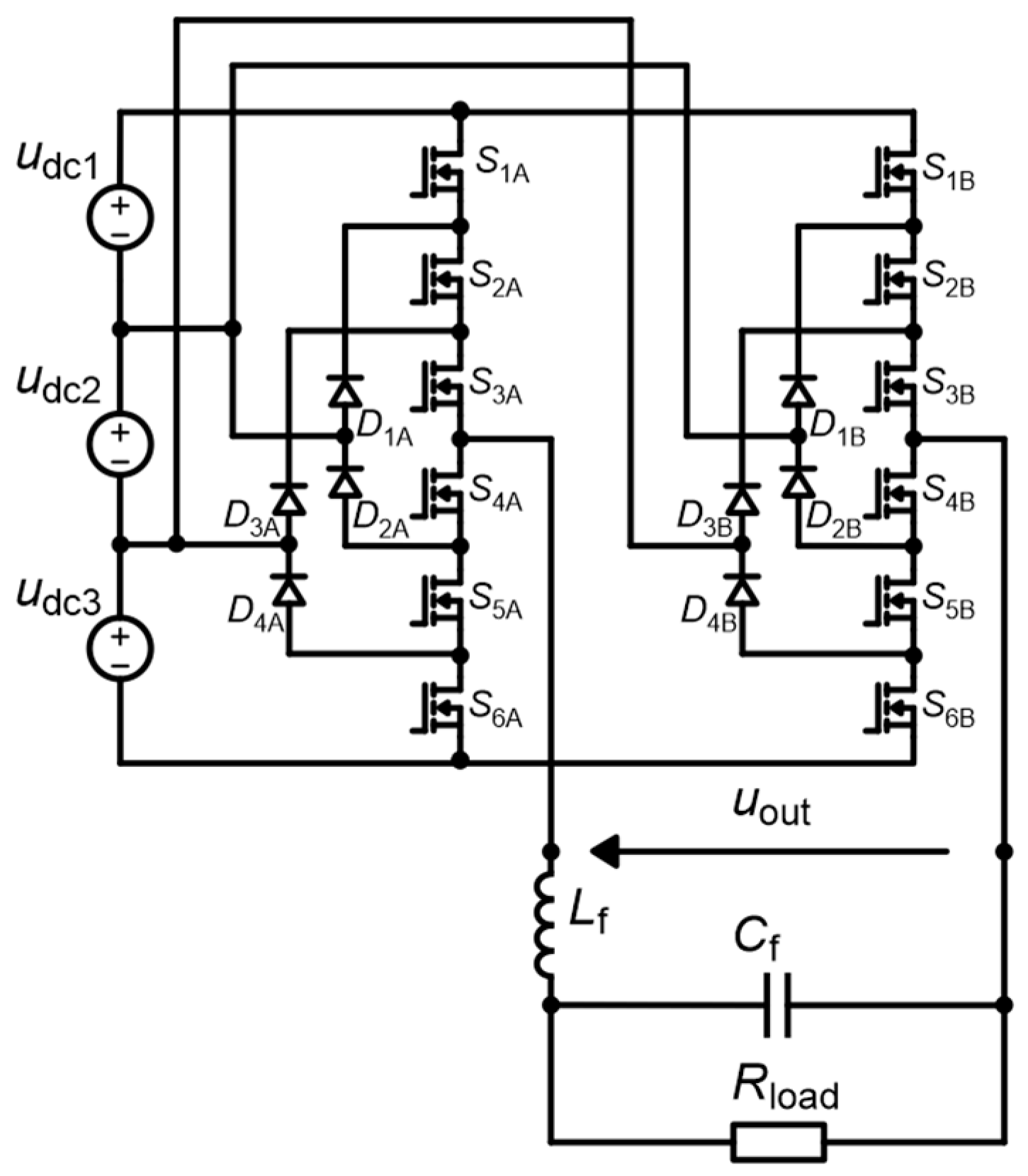
Figure 1 presents the general concept of the 7LDCB inverter. Each branch of the inverter allows for the generation of four voltage levels, and the output voltage can be modulated using seven levels. The inverter will be tested in a single-phase configuration with 400 V on the DC link. In such a configuration, the inverter will be designed with the use of MOSFETs and Schottky diodes with a voltage of 200 V. Such a system can be used as a single-phase grid-connected inverter. One of the most important research problems is achieving high efficiency in converters, which is why the research presented in this article is devoted to this issue. There are the following research aspects that are unique in relation to previous studies:
  • Efficiency analysis in a high-frequency circuit based on MOSFETs and Schottky diodes;
  • Studies of the influence of the switching frequency on the efficiency of the system in the range of 100–300 kHz;
  • Studies of the influence of the applied modulation on the efficiency of the system and the uniformity of the distribution of energy losses in its components;
  • Simulation studies of energy losses and converter efficiency with the use of physical elements implemented in the Matlab/Simulink environment with the Simscape library;
  • Hardware implementation of the modulation algorithm for research with the use of the Imperix RCP system, developed in MATLAB/Simulink R2022b Software.

2.2. Modulation Concepts

Two types of modulation will be used for the inverter studies, namely carrier-based modulation and modulation with a selective selection of DC-link capacitors used, algorithmically implemented using a state machine (SM). Since both types of modulation have a specific concept, they are labeled more specifically as carrier-based M1 and SM-based M2.
The 7LDCB inverter allows the generation of seven levels of voltage between phases, with some of the output voltage states being obtained redundantly. Table 1 lists the positive output voltage values, the states of the system components, and the number of DC-link capacitors used. Negative states can be obtained on the principle of symmetry.
In an NPC diode-camped inverter with a number of levels greater than 3, the use of classic carrier-based modulation causes uneven loading of the DC-link capacitors and an unbalanced problem with input divider voltages. However, such modulation is presented in the publication [5] in a system in which the DC voltage sources are not supplying the entire DC-link but the capacitor, which is discharged with the greatest power by the inverter. In cooperation with an external active balancing system, the inverter has gained the feature of a step-up system that works with partial conversion in the DC-DC part. Such modulation will be considered in this article as a reference for the comparison of energy losses and will be designated as M1 carrier-based.
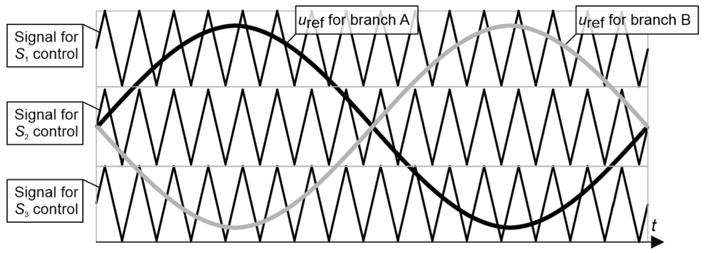
The M1 modulation is achieved in a carrier-based system, as presented in Figure 2. This modulation uses the order of the state presented in Table 2.
DC-link capacitor use by M1 (carrier-based) modulation is such that the center capacitor is overloaded at individual levels, which causes voltage imbalances on the input divider (Table 2). At the 0-to-1 and 1-to-2 modulation levels, capacitor C2 is used most often, which is disadvantageous, except in cases where this capacitor is sipped from an energy source, as shown in [3] in a circuit with an active voltage balancer on the DC-link.
The occurrence of redundant states allows voltage control on input capacitors.
In order to ensure uniform discharge of DC-link capacitors, it is advantageous to implement modulation based on the selective selection of DC-link capacitors used. The method proposed in the literature [4] evenly uses capacitors C1, C2, and C3 at each modulation level. The pulse width can be realized using the classic carrier-based method. Next, the state machine-based (SM-based) algorithm selects the implementation of the appropriate order of states of modulation and DC-link capacitors (Table 1) according to the algorithm presented in Table 3.
The SM-based modulation M2 presented by the algorithm in Table 3 at levels one and three uses states 1a, 1b, and 1c consecutively with the same frequency, and at level 2, it uses only states 1a and 1c because each state of level 2 (2a and 2b) uses capacitor C2. DC-link capacitor use by SM-based M2 modulation is such that the use of DC-link capacitors by the inverter is uniform and within the period of fundamental frequency. Reference [4] also proposes a switching pattern modifying SM-based M2, so states 1a, 1b, and 1c are implemented in the concordant and opposite order, which may affect the number of commutations during the pulsing period. This algorithm can be written as follows:
M3 states order for levels 0–1: {1a, 0, 1b, 0, 1c, 0, 1c, 0, 1b, 0, 1a, …},
M3 states order for levels 1–2: {1a, 2a, 1c, 2b, …},
M3 states order for levels: 1–3: {3, 1a, 3, 1b, 3, 1c, 3, 1c, 3, 1b, 3, 1a, 1a, …}

3. Simulation Research

The objective of the simulation research was to analyze and compare the power loss distribution in semiconductor components in a sample design of the inverter using M1 and M2 modulation. Simulation research was conducted in Matlab/Simulink R2022b using the Simscape library of physical elements. The aim of this research was to analyze the influence of the modulation patterns M1 and M2 in an example implemented design on the distribution of losses in semiconductor components. Measurements of the efficiency of the entire converter were carried out experimentally.
Table 4 presents the parameters of the elements used in the simulation model. All other parameters of transistors and diodes, as well as parasitic resistances of circuits and passive components, were included in the simulation model. The simulation was carried out with a variable calculation step.
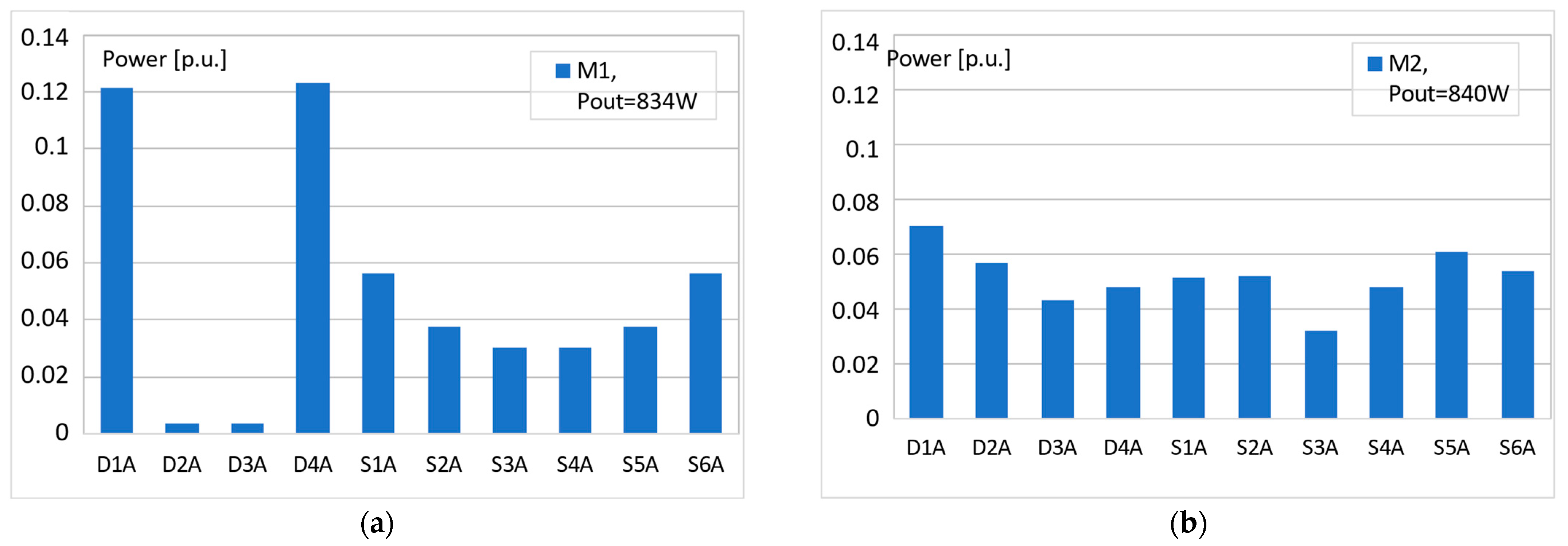
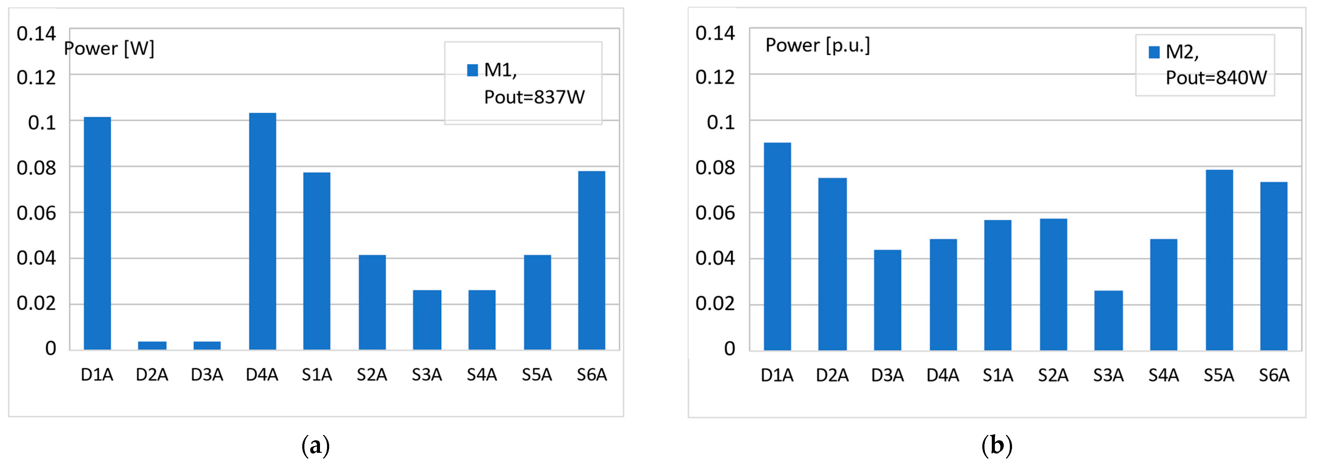
The results shown in Figure 3 and Figure 4 show that the distribution of power losses in the converter components is more even when M2 modulation is used. In a system with Schottky diodes, the power losses due to conduction in the diodes become comparable in the case of M2 modulation. For this modulation (M2) at a switching frequency of 100 kHz, the losses in MOSFETs and losses in diodes become comparable. This is due to the presence of conduction losses and significant values of Coss junction losses in MOSFETs. A comparison of the results from Figure 3 and Figure 4 shows the significant influence of the output capacitance of the transistor on the power losses in the tested system.
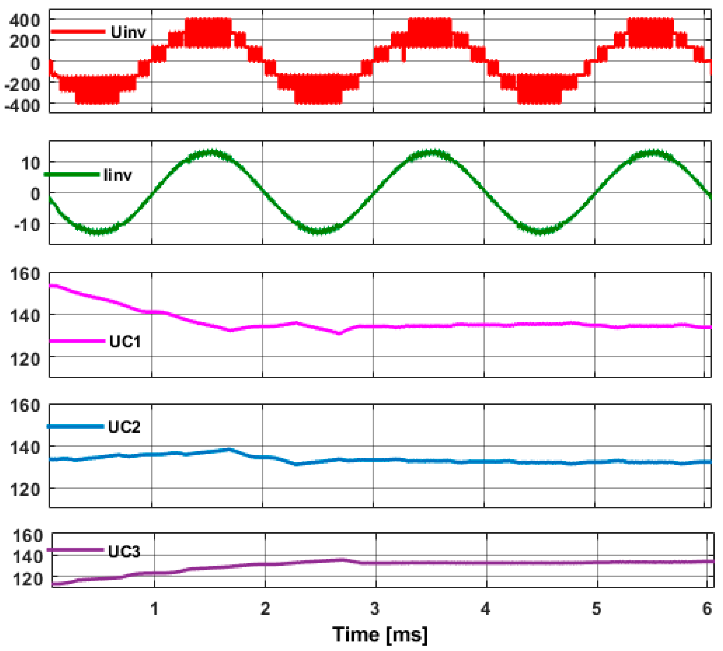
The SM-based M2 modulation is based on the selective selection of the loaded DC-link capacitor. Thus, it enables the implementation of the algorithm of DC-link voltage balancing. In the exemplary algorithm, the result of which is presented in Figure 5, a change in the index of the loaded capacitor was used when the inverter performed modulation. In the basic SM-based M2 algorithm, the voltages from capacitors C1, C2, and C3 are used alternately (Table 3). In the unbalanced state, this algorithm has been replaced by switching using the highest voltage capacitor in the unbalanced state.

4. Experimental Tests

4.1. Experimental Setup

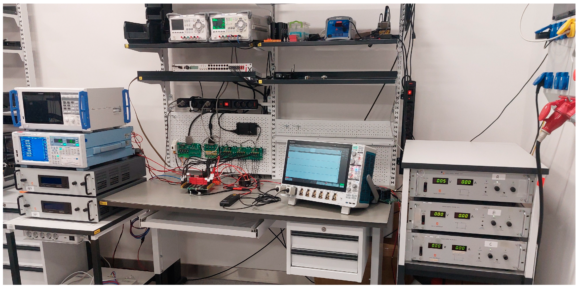
To perform experimental verification of the analyzed converter, a laboratory setup was prepared. The setup consists of the inverter itself, three independent power supplies, an output LC filter, and a control system based on the IMPERIX RCP B-box device as presented in Figure 6.
In the experimental setup, the 7LDCB inverter, composed of IPB073N15N5 transistors and VBT10202C Schottky diodes, is used, as shown in Figure 7.
During experimental and simulation tests of the inverter, DC-link voltages are supported by independent sources, as displayed in Figure 8, which allows for precise inverter efficiency results.
The detailed test conditions and hardware-related parameters of the proposed inverter are listed in Table 5.
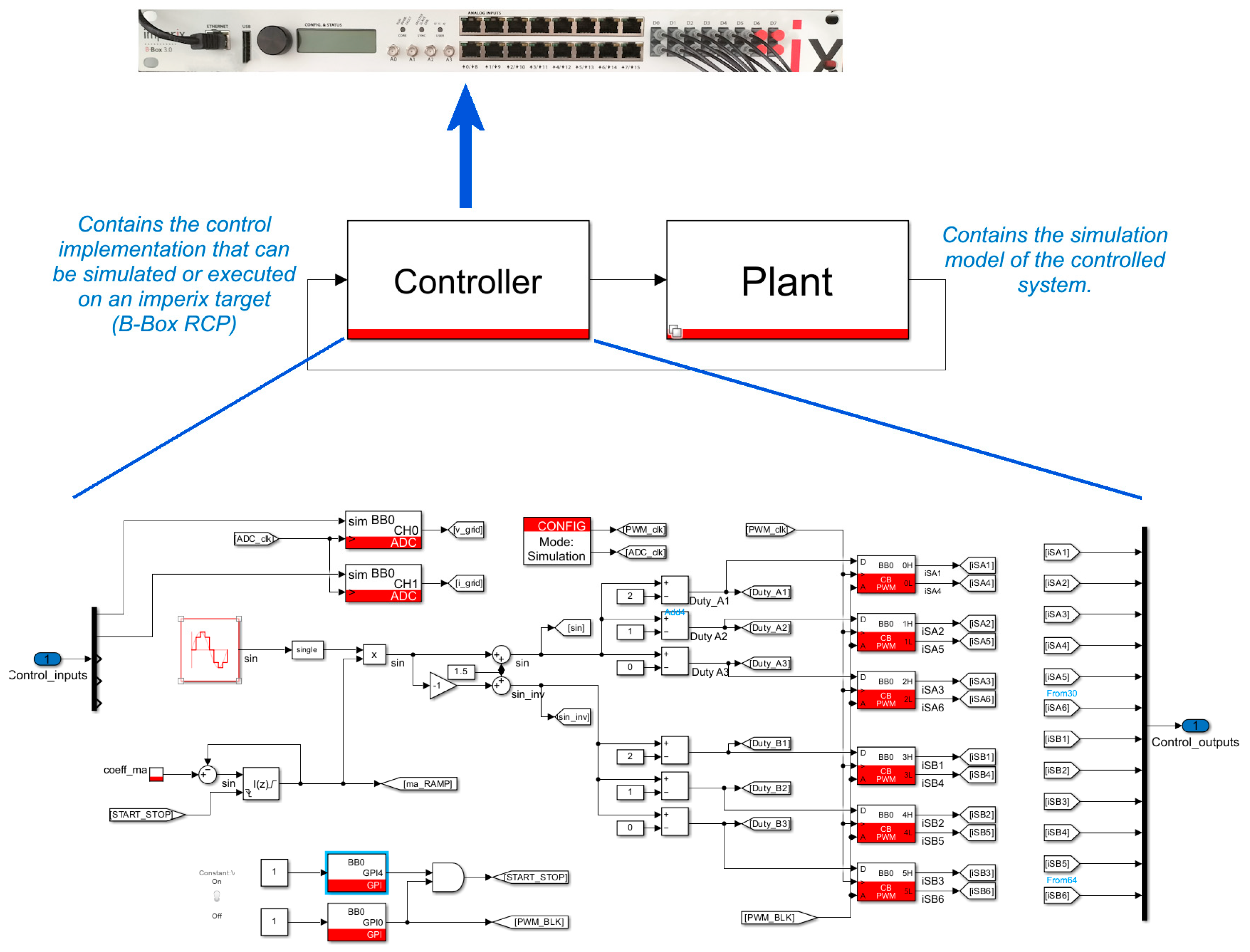
Control signals for the transistors were provided by the rapid control prototyping system, IMPERIX B-Box. The B-Box RCP is a fully programmable DSP+FPGA controller dedicated to power electronic converters. The controller is based on the Xilinx Zynq Z-7030 with a Kintex 7 125 k FPGA at 250 MHz and 2 ARM Cortex A9 CPUs operating at 1 GHz. Thanks to the use of this solution, it was possible to prepare and test the model in the Matlab/Simulink environment and then automatically generate the code and program the controller. The modulation of the switching signals was designed in the Matlab/Simulink version R2022b environment, according to the carrier-based M1 and SM-based M2 strategies. In the case of M2 modulation, it was necessary to design a dedicated PWM modulator implemented directly in the FPGA of the controller. The concept of the control system is shown in Figure 9.
The flexibility of the IMPERIX system in terms of in-flight parameter change was very useful, and thanks to this feature, it was possible to easily and accurately tailor parameters like switching frequency, modulation index, and switching dead-time to their optimal values.

4.2. Experimental Results

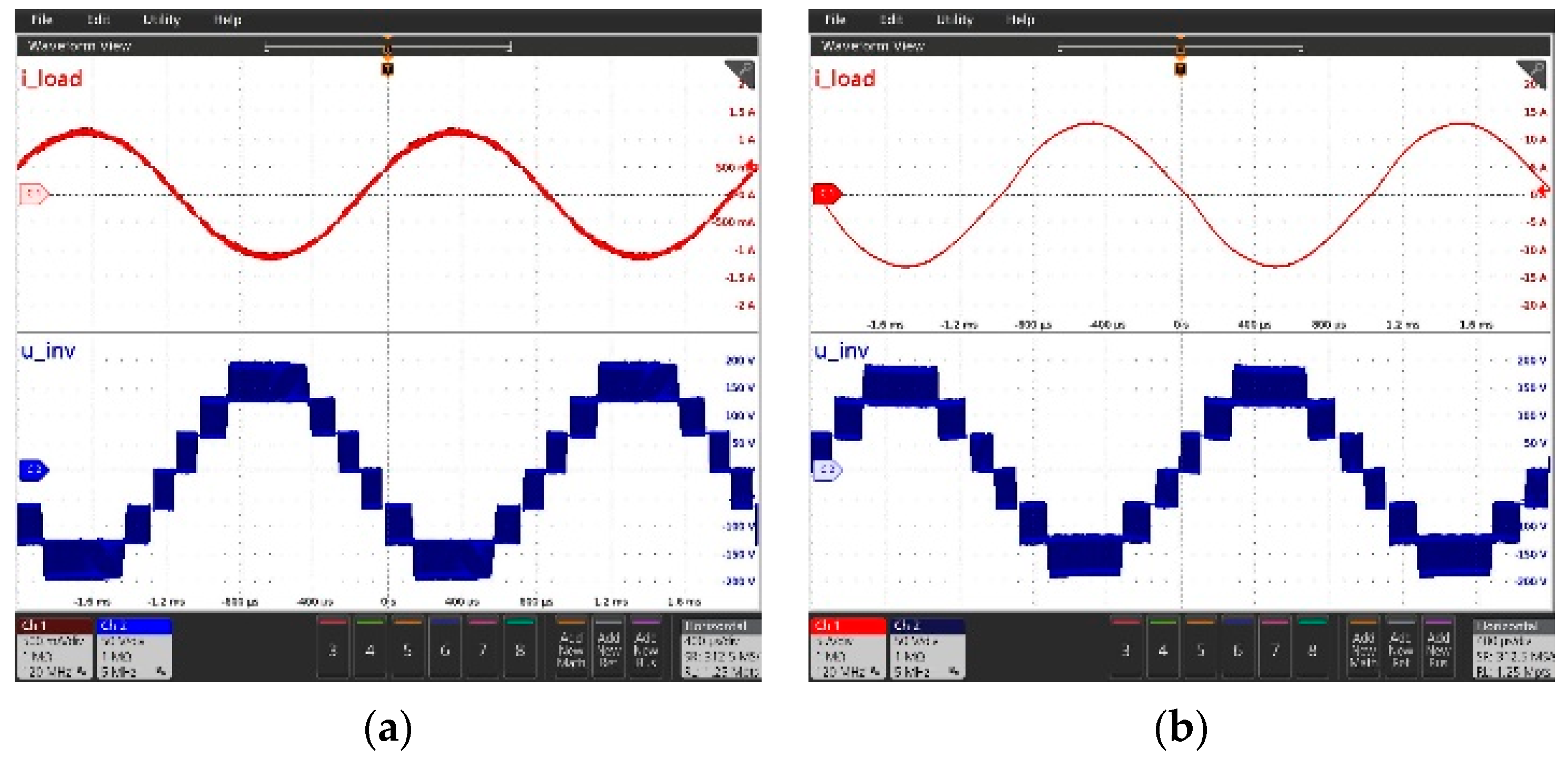
During the experimental evaluation of the high-frequency 7LDCB inverter, several measurements and tests were conducted. After the first power-up, the correctness of the proposed converter operation was confirmed using two modulation strategies. To prove the device operates as it was assumed, measurements of the unfiltered output voltage of the inverter and its load current were performed. The waveforms are shown in Figure 10 and Figure 11.
High-frequency operation can be beneficial due to the reduction in the volume of passive components. However, this can lead to large connection losses, which is why in the next stage of the experimental research on the proposed inverter, a study of the device’s efficiency was performed. During experiments, three efficiency curves were collected for different switching frequencies. They are shown in Figure 12. The best results were obtained for the switching frequency of 100 kHz. Two remaining curves, visible in Figure 12, were captured at 200 and 300 kHz of the switching frequency. From this graph, it is seen that switching frequency increases cause a decrease in the device’s efficiency, especially within the range of output powers lower than 400 W. Nevertheless, the device’s peak efficiency is surprisingly good and reaches a value of nearly 98%. Furthermore, the difference in peak efficiency between the 100 and 200 kHz switching frequency operations is very small.
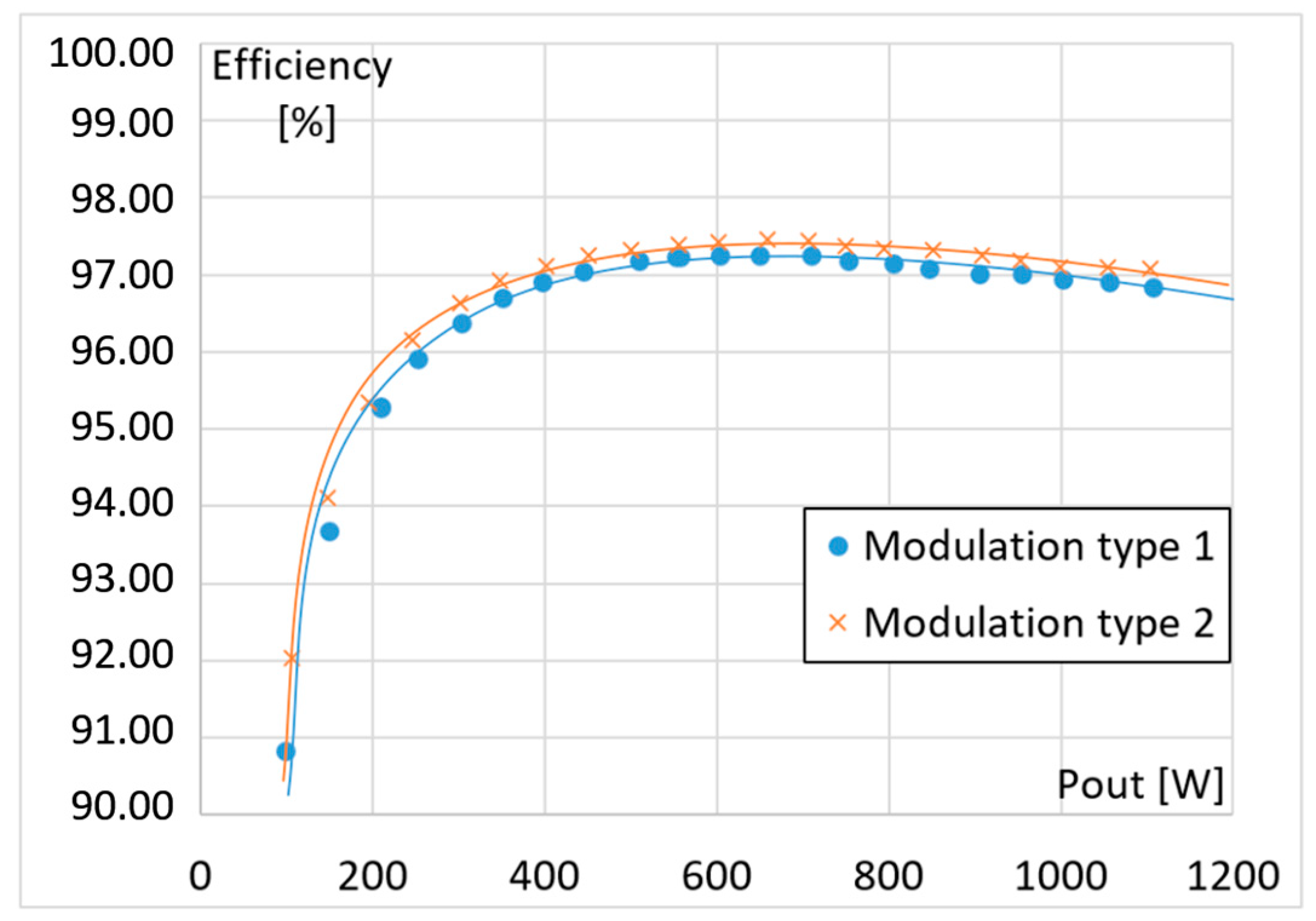
Strategies of carrier-based M1 and SM-based M2 modulation were experimentally compared in terms of efficiency and loss distribution in individual components. Figure 13 shows a comparison of the inverter efficiency for M1 and M2 modulation at a switching frequency of 200 kHz. A very important conclusion from these measurements is that an inverter operating with M2 modulation achieves higher efficiency over the entire power range. This may be the result of a more uniform load of devices and the use of the connection elements in the converter. It results in a reduction of resistive proportional losses, which are a quadratic function of the current. This is very advantageous because M2 modulation also ensures that DC-link voltages are balanced, making it an overall better option than carrier-based M1.
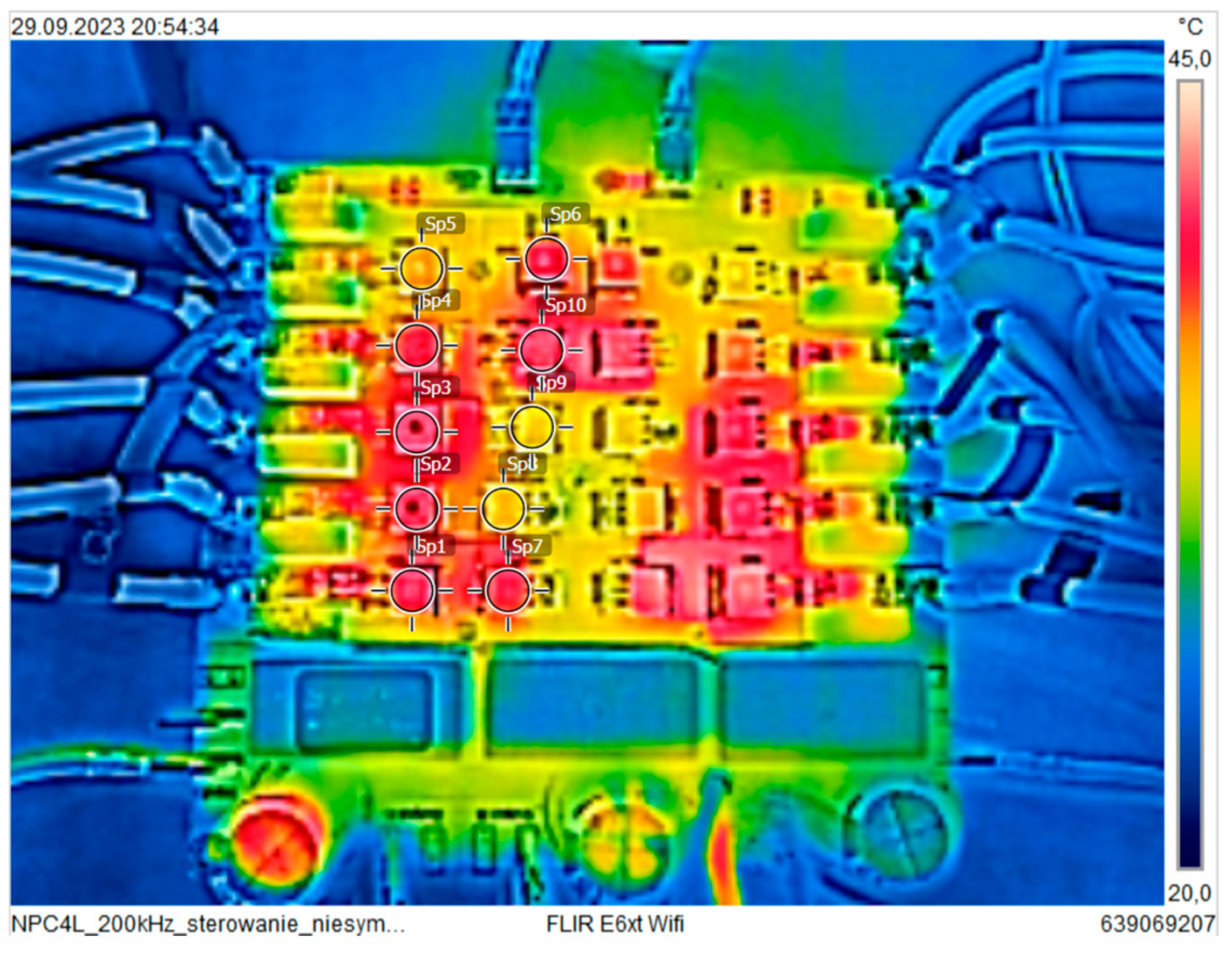
Figure 14, Figure 15 and Figure 16 show the results of thermal imaging measurements of temperature on the housings of transistor element diodes of A-phase at the switching frequency fs = 200 kHz and the output power Pout = 550 W. The results presented in Figure 14 and Figure 15 characterize the operation of the system with M1 modulation, while the results presented in Figure 16 are a comparison of the temperature of the system when controlled with M1 and M2 modulation. The temperature measurement points are shown in Figure 14 (Sp1–Sp10). All results shown in Figure 14, Figure 15 and Figure 16 are on the same color-related temperature scale that is located to the right of each thermal image.
Figure 15 shows the temperature measurement results for different switching frequencies used for the inverter operation. An increase in the temperature of the inverter components is visible as the pulsing frequency increases, especially in this type of transistor. However, increasing the pulsing frequency from 100 to 200 kHz does not significantly increase the heating rate of the components. This is achieved by lowering the voltage stress in the 4-level branch inverter and reducing switching losses. However, the increase in temperature with the increase in switching frequency is more clearly seen in the transistor cases rather than in diodes in this design based on MOSFETs and Schottky rectifiers.
Figure 16 shows a comparison of the thermal imaging results of the inverter components using carrier-based M1 and SM-based M2 modulation one minute after switching on the inverter with a power of Pout = 550 W. From these results, it is clear that the M2 modulation results in a more even distribution of energy losses in the elements. This is in line with the assumptions of this modulation method, according to which DC-link capacitors and active components are used symmetrically at each level.
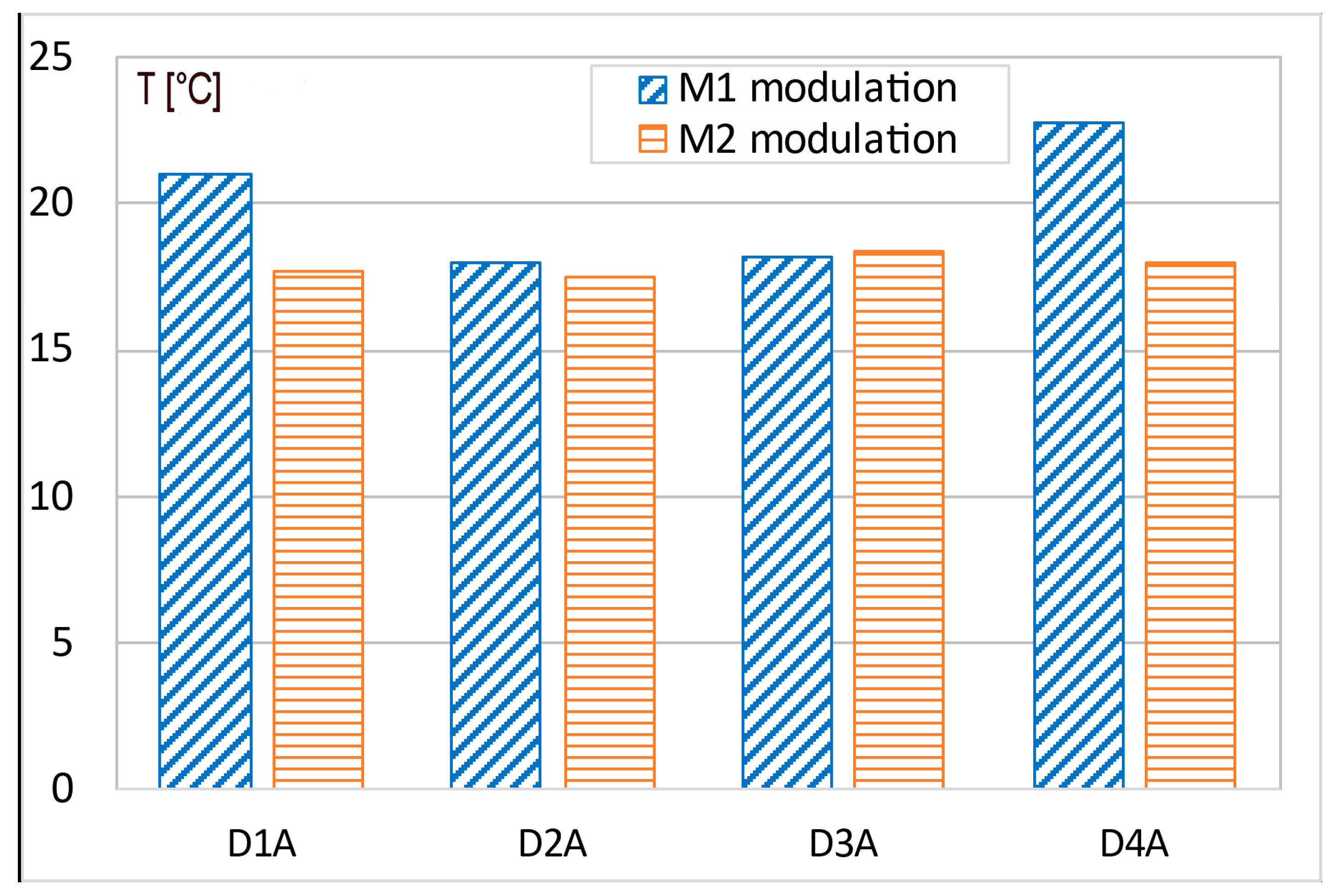
Figure 17 shows a comparison of the temperature of the Phase A elements of the system obtained on the basis of thermal imaging registration 10 min after switching on the system with an active power of 550 W. This is a very significant result that shows that the heating rate of the components with the SM-based M2 symmetrical control is lower, and most of the elements have a similar temperature. The distribution of losses is more even. The exact efficiency measurement results shown in Figure 16 also showed a higher efficiency of the inverter when using the SM-based M2 control method.

5. Conclusions

The analyzed MOSFET-based diode clamped single-phase bridge composed of four-level legs achieved 97.8% efficiency, which can be considered high compared to the results of several dozen inverters summarized in [2], whose reported efficiency was in the range of 94.09–99.25%. Reduction of voltage stress across semiconductor devices in such a topology allows for the use of low RDS(on) devices, reducing conduction losses, which leads to increased converter efficiency. Coss losses are reduced significantly as well since the energy dissipated from the transistors’ output capacitance is reduced. Reduction of voltage across diodes to values much below 200 V allows the use of Schottky diodes of very low forward voltage VF, which gives an important reduction in conduction losses in diodes.
The implementation of levels higher than 3 for the phases of the NPC diode-clamped inverter is possible by using appropriate modulation. A hardware implementation of the modulation based on selective state use is presented in this article for an inverter operating at a switching frequency of 200 kHz. The analysis of this type of modulation from the point of view of the inverter’s efficiency and the distribution of losses in the components is an original result and shows the positive properties of this method. The method based on selective state use has three significant advantages, as it allows for even distribution of the load of DC-link capacitors, even distribution of losses and temperature in converter components, and high efficiency. This is an important result, indicating that a diode-clamped bridge inverter can be designed for more than three levels of voltage modulation in phase. This reduces the voltage stress across the components and allows the use of components with better parameters, such as RDS(on) of MOSFETs or VF of diodes. In the analyzed case, the inverter operating at a DC voltage of 400 V was configured with the use of MOSFETs and Schottky diodes with a voltage of 200 V. The test was carried out for a switching frequency of up to 300 kHz, and the increase in frequency from 100 to 200 kHz did not cause a significant decrease in inverter efficiency. The practical significance of the analyzed modulation method with selective selection of DC-link capacitors (SM-based) is also important, as it simplifies the thermal design for the inverter and the selection of system components and protects DC-link from imbalance.
The second, classic carrier-based modulation method has a significant disadvantage because it generates a DC-link voltage imbalance and also shows lower efficiency in the tested inverter and less uniform distribution of losses and temperature of system elements. The advantage of this method is that it can be used in systems where the middle capacitor of the inverter is supplied and the two remaining capacitors are charged by an external balancing system with a power much lower than the rated power.
To summarize, a proper modulation strategy allows the operation of an NPC-type inverter with DC-link voltage balance control, improved efficiency, and a more even temperature distribution.

Author Contributions

Conceptualization, R.S.; methodology, R.S. and A.P.; software, R.S., A.P. and S.F.; validation, R.S., J.H., S.F., Z.M. and A.P.; formal analysis, R.S.; investigation, R.S., J.H., S.F., Z.M. and A.P.; resources, R.S.; and A.P.; data curation, R.S., J.H. and S.F.; writing—original draft preparation, R.S., S.F., Z.M. and A.P.; writing—review and editing, R.S., S.F., Z.M. and A.P.; visualization, R.S.; supervision, R.S.; project administration, R.S.; funding acquisition, R.S. and A.P. All authors have read and agreed to the published version of the manuscript.

Funding

This research received no external funding.

Data Availability Statement

Data are contained within the article.

Acknowledgments

Research project partly supported by program “Excellence initiative—research university” for the AGH University of Krakow. This research was supported by the AGH Interdisciplinary Research Laboratory (www.ilb.agh.edu.pl, accessed on 16 October 2023).

Conflicts of Interest

Author Jakub Hachlowski was employed by the company SMA-Magnetics Sp. z o.o. The remaining authors declare that the research was conducted in the absence of any commercial or financial relationships that could be construed as a potential conflict of interest.

References

  1. Shieh, J.-J.; Hwu, K.-I.; Chen, S.-J. Perspective of Voltage-Fed Single-Phase Multilevel DC-AC Inverters. Energies 2023, 16, 898. [Google Scholar] [CrossRef]
  2. Khan, M.N.H.; Forouzesh, M.; Siwakoti, Y.P.; Li, L.; Kerekes, T.; Blaabjerg, F. Transformerless Inverter Topologies for Single-Phase Photovoltaic Systems: A Comparative Review. IEEE J. Emerg. Sel. Top. Power Electron. 2020, 8, 805–835. [Google Scholar] [CrossRef]
  3. Anderson, J.A.; Zulauf, G.; Papamanolis, P.; Hobi, S.; Mirić, S.; Kolar, J.W. Three Levels Are Not Enough: Scaling Laws for Multilevel Converters in AC/DC Applications. IEEE Trans. Power Electron. 2021, 36, 3967–3986. [Google Scholar] [CrossRef]
  4. Stala, R. Natural DC-link voltage balance in a single-phase NPC inverter with four-level legs and novel modulation method. IET Power Electron. 2020, 13, 3764–3776. [Google Scholar] [CrossRef]
  5. Stala, R.; Hachlowski, J.; Penczek, A. NPC Seven-Level Single-Phase Inverter with DC-Link Voltage Balancing, Input Voltage Boosting, and AC Power Decoupling. Energies 2022, 15, 3729. [Google Scholar] [CrossRef]
  6. Mecke, R. Multilevel Inverter with New Wide-Bandgap SiC and GaN Power Switches. In Proceedings of the 2021 IEEE 15th International Conference on Compatibility, Power Electronics and Power Engineering (CPE-POWERENG), Florence, Italy, 14–16 July 2021; pp. 1–6. [Google Scholar] [CrossRef]
  7. Mecke, R. Wide-bandgap Semiconductors for Multilevel Inverters—A Comparison with Si IGBT. In Proceedings of the 2023 International Conference on Electrical Drives and Power Electronics (EDPE), The High Tatras, Slovakia, 25–27 September 2023; pp. 1–6. [Google Scholar] [CrossRef]
  8. Rojas, R.; Ohnishi, T.; Suzuki, T. PWM control method for a four-level inverter. IEE Proc. Electr. Power Appl. 1995, 142, 390–396. [Google Scholar] [CrossRef]
  9. Wang, K.; Zheng, Z.; Li, Y. A novel carrier-overlapped PWM method for four-level neutral-point clamped converters. IEEE Trans. Power Electron. 2019, 34, 7–12. [Google Scholar] [CrossRef]
  10. Wang, K.; Zheng, Z.; Xu, L.; Li, Y. A composite voltage balancing method for four- level NPC inverters. IEEE J. Emerg. Sel. Top. Power Electron. 2020, 9, 3394–3406. [Google Scholar] [CrossRef]
  11. Busquets-Monge, S.; Ruderman, A. Carrier-based PWM strategies for the comprehensive capacitor voltage balance of multilevel multileg diode-clamped converters. In Proceedings of the 2010 IEEE International Symposium on Industrial Electronics, Bari, Italy, 4–7 July 2010; pp. 688–693. [Google Scholar]
  12. Strzelecki, R.; Szczepankowski, P.; Strzelecka, N. Four level diode-clamped back-to-back converter with active DC link voltage control. In Proceedings of the 2013 International Conference-Workshop Compatibility and Power Electronics, Ljubljana, Slovenia, 5–7 June 2013; pp. 182–187. [Google Scholar]
  13. Hachlowski, J.; Stala, R. DC-link Voltage Balancing Converter with Resonant Switched-Capacitor Circuit for Four-Level and Six-Level NPC Inverter. In Proceedings of the 2019 21st European Conference on Power Electronics and Applications (EPE 19 ECCE Europe), Genova, Italy, 3–5 September 2019. [Google Scholar]
  14. Kuo, S.-H.; Lin, Z.-A.; Liu, Y.-H.; Hsieh, Y.-C.; Chiu, H.-J. Study and Implementation of a Single-Phase Diode- Clamped Five-Level Inverter with Auto Equalization. In Proceedings of the 2018 Asian Conference on Energy, Power and Transportation Electrification (ACEPT), Singapore, 30 October–2 November 2018. [Google Scholar]
  15. Maheshwari, R.; Busquets-Monge, S.; Nicolas-Apruzzese, J. A novel approach to generate effective carrier-based pulse width modulation strategies for diode-clamped multilevel DC–AC converters. IEEE Trans. Ind. Electron. 2016, 63, 7243–7252. [Google Scholar] [CrossRef]
  16. Dutta, S.; Negi, S.; Yadav, A.K.; Tripathi, A. A New Carrier Based PWM for a 3-Phase 5-Level Neutral Point Clamped Inverter. In Proceedings of the 2023 IEEE 3rd International Conference on Sustainable Energy and Future Electric Transportation (SEFET), Bhubaneswar, India, 9–12 August 2023. [Google Scholar]
  17. Carrara, G.; Gardella, S.; Marchesoni, M.; Salutar, R.; Sciutto, G. A new multilevel PWM method: A theoretical analysis. IEEE Trans. Power Electron. 1992, 7, 497–505. [Google Scholar] [CrossRef]
  18. Bharathsrinivas, R.; Angadi, S.; Hombal, G.; Raju, A.B. Investigation of Diode Clamped Multilevel Inverter Using Multicarrier PWM Techniques. In Proceedings of the 2021 IEEE International Conference on Electronics, Computing and Communication Technologies (CONECCT), Bangalore, India, 9–11 July 2021. [Google Scholar]
  19. Sarker, R. Phase Disposition PWM (PD-PWM) Technique to Minimize WTHD from a Three-Phase NPC Multilevel Voltage Source Inverter. In Proceedings of the 2020 IEEE 1st International Conference for Convergence in Engineering (ICCE), Kolkata, India, 5–6 September 2020; pp. 220–224. [Google Scholar] [CrossRef]
  20. Stala, R. Nine-level inverter based on NPC topology for high frequency operation. In Proceedings of the 2023 25th European Conference on Power Electronics and Applications (EPE’23 ECCE Europe), Paris, France, 4–8 September 2023. [Google Scholar]
  21. Li, C.; Chen, J. Simplified SVPWM Capacitor Voltage Balancing Control Method for Four-Level Neutral Point Clamped Inverters. In Proceedings of the 2023 IEEE 14th International Symposium on Power Electronics for Distributed Generation Systems (PEDG), Shanghai, China, 9–12 June 2023; pp. 127–132. [Google Scholar] [CrossRef]
  22. Najah, A.; Essalam, B.A.; Merahi, F.; Laib, A.; Lazhar, R. Performance Analysis of Four Level NPC Inverters using FCS-MPC Voltage Balancing Method. In Proceedings of the 2022 19th International Multi-Conference on Systems, Signals & Devices (SSD), Sétif, Algeria, 6–10 May 2022; pp. 1450–1455. [Google Scholar] [CrossRef]
  23. Wang, J.; Yuan, X.; Jin, B. Carrier-based Closed-loop DC-link Voltage Balancing Algorithm for Four Level NPC Converters Based on Redundant Level Modulation. IEEE Trans. Ind. Electron. 2021, 68, 11707–11718. [Google Scholar] [CrossRef]
  24. Wang, J.; Xu, W.; Yuan, X.; Xie, L. Investigation and Mitigation of Common-mode Voltage in Four-level NPC Converters Modulated by Redundant Level Modulation. In Proceedings of the 2022 24th European Conference on Power Electronics and Applications (EPE’22 ECCE Europe), Hanover, Germany, 5–9 September 2022; pp. 1–9. [Google Scholar]
  25. Gopi, A.K.; Kumar, M.A.; Biswas, J.; Barai, M. An Optimized Hybrid PWM Strategy for Five Level NPC VSI With Unequal DC-Links in a PV System. IEEE J. Emerg. Sel. Top. Ind. Electron. 2022, 3, 766–776. [Google Scholar] [CrossRef]
  26. Pham, L.N.; Phan, Q.D.; Nguyen, N.-V. Simplified Space Vector Pulse Width Modulation for Four-Level Neutral Point Clamped Inverter. In Proceedings of the 2023 International Symposium on Electrical and Electronics Engineering (ISEE), Ho Chi Minh, Vietnam, 19–20 October 2023; pp. 244–249. [Google Scholar] [CrossRef]
  27. Tolbert, L.M.; Habetler, T.G. Novel multilevel inverter carrier-based PWM method. IEEE Trans. Ind. Appl. 1999, 35, 1098–1107. [Google Scholar] [CrossRef]
Figure 1. General concept of a seven-level diode-clamped bridge (7LDCB) inverter with four-level branches.
Energies 16 07866 g001
Figure 2. M1 carrier-based modulation for 7LDCB [5].
Energies 16 07866 g002
Figure 3. Simulation results of the loss distribution in the A-phase elements of an inverter using carrier-based M1 modulation (a) and SM-based M2 modulation (b). P. u. results are related to total losses in semiconductor devices. Rds(on) = 30 mΩ, Coss = 395 pF.
Energies 16 07866 g003
Figure 4. Simulation results of the loss distribution in the A-phase elements of an inverter using carrier-based M1 modulation (a) and SM-based M2 modulation (b). P. u. results are related to total losses in semiconductor devices. Rds(on) = 12 mΩ, Coss = 900 pF.
Energies 16 07866 g004
Figure 5. Imbalance reduction by using the SM-based M2 strategy with implemented overloading of the DC-link with the highest voltage.
Energies 16 07866 g005
Figure 6. Laboratory test setup for power losses and efficiency measurements.
Energies 16 07866 g006
Figure 7. PCB board for the 7LDCB inverter implementation.
Energies 16 07866 g007
Figure 8. The tested inverter configuration with DC-power supply.
Energies 16 07866 g008
Figure 9. Control system configuration based on Matlab/Simulink and IMPERIX B-Box RCP system.
Energies 16 07866 g009
Figure 10. Steady state of operation with the output power at levels of 100 W (a) and 1000 W (b) and modulation type carrier-based M1. Load current (CH1) and unfiltered output voltage of the proposed inverter (CH2).
Energies 16 07866 g010
Figure 11. Steady state of operation with the output power on the level of 100 W (a) and 1000 W (b) and modulation type SM-based M2. Load current (CH1) and unfiltered output voltage of the proposed inverter (CH2).
Energies 16 07866 g011
Figure 12. Efficiency curves of the proposed inverter at three different switching frequencies for carrier-based M1 modulation strategy in the range of output power 50–1000 W.
Energies 16 07866 g012
Figure 13. Efficiency curves of the 7LDCB inverter performed with two different modulation types (type 1: carrier-based M1, type 2: SM-based M2) at a switching frequency of 200 kHz. Efficiency is calculated as the ratio of the output to the input power of the inverter from all three power supply units.
Energies 16 07866 g013
Figure 14. Temperature measurement points on transistors and diodes housings of A-phase (fs = 200 kHz, Pout = 550 W). Carrier-based M1 modulation method.
Energies 16 07866 g014
Figure 15. Results for carrier-based M1 modulation for various switching frequencies: 100 kHz (a), 200 kHz (b), and 300 kHz (c) for Pout = 550 W, Q = 0 Var, after 1 min from the start of the converter.
Energies 16 07866 g015
Figure 16. Results for carrier-based M1 (a) and selective SM-based M2 (b) modulation strategies. Temperature measurement on the transistor and A-phase diode housings for switching frequency 200 kHz, Pout = 550 W, Q = 0 Var, after 1 min from the start of the converter.
Energies 16 07866 g016
Figure 17. Results based on thermal imaging registration for carrier-based M1 and selective SM-based M2. Temperature measurement on the housings of the transistor and A-phase diode components for switching frequency 200 kHz, Pout = 550 W, Q = 0 Var, after 10 min from the start of the converter.
Energies 16 07866 g017
Table 1. Three positive voltage levels generation in 7LDCB.
Level 1
and State Name
Used Switches and DC-Link Capacitors
{S1A, S2A, S3A, S4A, S5A, S6A}{S1B, S2B, S3B, S4B, S5B, S6B}DC-Link
Capacitor
3{1, 1, 1, 0, 0, 0}{0, 0, 0, 1, 1, 1}C1, C2, C3
2 (2a){1, 1, 1, 0, 0, 0}{0, 0, 1, 1, 1, 0}C1, C2
2 (2b){0, 1, 1, 1, 0, 0}{0, 0, 0, 1, 1, 1}C2, C3
1 (1a){1, 1, 1, 0, 0, 0}{0, 1, 1, 1, 0, 0}C1
1 (1b){0, 1, 1, 1, 0, 0}{0, 0, 1, 1, 1, 0}C2
1 (1c){0, 0, 1, 1, 1, 0}{0, 0, 0, 1, 1, 1}C3
1 Voltage level is presented as p.u.: uout/(Uin/3).
Table 2. States order in carrier-based modulation M1.
Modulation Step 1 (One or Two Repetition Periods),
and DC-Link Capacitor Use
nn + 1n + 2n + 3
Levels used for modulation0–1state:1b
C2
0
none
1b
C2
0
none
1–2state:1b
C2
2a
C1, C2
1b
C2
2b
C2, C3
2–3state:2a
C1, C2
3
all
2b
C2, C3
3
all
1 n is an index of realization of the next modulation state.
Table 3. States order in SM-based modulation M2.
Modulation Step 1 (One Repetition Periods),
and DC-Link Capacitor Use
nn + 1n + 2n + 3n + 4n + 5
Levels used for modulation0–1State:1a
C1
0
None
1b
C2
0
None
1c
C3
0
None
1–2State:1a
C1
2a
C1, C2
1c
C3
2b
C2, C3
2–3State:1a
C1
3
All
1b
C2
3
All
1c
C3
3
All
1 n is an index of realization of the next modulation state.
Table 4. The main simulation model parameters for power loss distribution assessment.
ParameterValue
All the MOSFETS Rds(on) [mΩ]12–30
MOSFETS COSS [pF]395 and 900
Schottky clamping diodes VF [V]0.72
Input voltage Uin [V]400
Switching frequency fS [kHz]100
Table 5. Parameters of the experimental system.
ParameterValue
TransistorsIPB073N15N5
UDS = 150 V
ID = 114 A
RDS(on) = 7.3 mΩ
DiodesVBT10202C-M3/4W
IF(AV) = 2 × 5 A
URRM = 200 V
UF = 0.65 V at IF = 5 A
LC filter150 uH/2 × 4.7 uF
Input voltage Uin400 (3 × 133) V
Switching frequency fS100–300 kHz
Output voltage Uout150 V (RMS)
Output power Pout50–1100 W
Disclaimer/Publisher’s Note: The statements, opinions and data contained in all publications are solely those of the individual author(s) and contributor(s) and not of MDPI and/or the editor(s). MDPI and/or the editor(s) disclaim responsibility for any injury to people or property resulting from any ideas, methods, instructions or products referred to in the content.