Article

A Fault-Tolerant Control Strategy for Three-Level Grid-Connected NPC Inverters after Single-Arm Failure with Optimized SVPWM

School of Information Engineering, Henan University of Science and Technology, Luoyang 471023, China
*
Author to whom correspondence should be addressed.
Energies 2023, 16(23), 7863; https://doi.org/10.3390/en16237863
Submission received: 21 September 2023 / Revised: 23 November 2023 / Accepted: 28 November 2023 / Published: 30 November 2023
(This article belongs to the Special Issue Power Electronic Converter and Its Control)

Abstract

:
Three-level NPC inverters have been widely used in grid-connected systems due to their superior performance compared with two-level inverters, but more switches lead to high fault probability. Meanwhile, the neutral point potential (NPP) fluctuation of the DC link is an inherent problem of three-level NPC inverters. To keep the three-level NPC inverter running stably after single-arm failure, a fault-tolerant control strategy based on an optimised space vector pulse width modulation (SVPWM) is proposed in this paper. Firstly, the common-mode voltage (CMV) of the postfault three-level NPC inverter is analysed and then the preliminary synthesis principles of the reference voltage vector are determined. Then, in order to ensure the NPP balance and the quality of the grid-connected currents, the reference voltage vector synthesis rules are optimised, a low-pass filter (LPF) and a hysteresis comparator are designed, respectively, to ensure the quality of grid-connected currents and effectively decrease the DC link NPP deviation. Finally, the simulation results show that the proposed fault-tolerant control strategy can realize the stable and reliable operation of the grid-connected three-level NPC inverter after single-arm failure, and the CMV can be reduced significantly, the quality of grid-connected currents is also improved. The proposed fault-tolerant strategy also shows good performance when the grid-connected currents change.

1. Introduction

The three-phase three-level neutral point clamped (NPC) grid-connected inverters can simplify the design of filter because their outputs are close to sine waves compared with the two-level inverters. Therefore, they have been widely used in grid-connected systems [1,2]. However, the failure probability of the three-level NPC inverters increases with the multiplied number of power semiconductor devices [3,4,5]. To ensure sustainable operation of the three-level NPC grid-connected inverters when there is a short-circuit or open-circuit on the bridge arm of a certain phase, it is crucial to conduct thorough research on grid-connected control of the inverters after single-arm failure.
When the single-arm of inverter is failure, fault-tolerant control proves to be an efficient method to ensure uninterrupted operation of the system. In the case of three-level NPC inverters, common fault-tolerant topologies include three-phase four-bridge arm fault-tolerant topologies [6,7], switching redundancy topologies [8,9], ANPC fault-tolerant topologies [10,11], and eight-switch three-phase fault-tolerant topologies [12,13], etc. In this paper, considering the cost, volume and control complexity, the eight-switch three-phase inverters (ESTPIS) are the topology for postfault three-phase three-level NPC grid-connected inverters.
For three-level NPC grid-connected inverters, the fluctuation of neutral point potential (NPP) can be a source of concern. This problem will not only increase the content of low-order harmonics in grid-connected currents, but also cause distortion in the inverter’s output voltage and create additional stress on the switch. When the NPP fluctuation is particularly severe, it can even impact the lifespan of DC-link capacitors, as noted in [14]. As a result, ESTPI as the fault-tolerant topology still has the issue of NPP fluctuation. For three-level NPC inverters, the virtual voltage vector pulse width modulation technique (VSVPWM) is utilized to synthesize the virtual vector to restrain the fluctuation of the NPP. In [15,16], the distribution coefficients of each basic vector in the virtual vector are recalculated to suppress the fluctuation of the NPP. However, the space voltage vectors of ESTPI no longer contain redundant voltage vectors [17], therefore the multi-vector method of suppressing NPP fluctuation is limited. It is also possible to control the NPP by setting the cost function through model predictive control, but there are challenges in selecting the NPP error weight factor, the filtering complexity, and high sampling frequency requirements [18,19]. For ESTPI, the space vector pulse width modulation (SVPWM) technology can be used to control the NPP. In [20], the control effect of two different SVPWM strategies on NPP is analysed under different voltage vector selections. In [21], the SVPWM avoids using the voltage vectors with high CMV and reduces the CMV while suppressing NPP fluctuation. In [22], due to the lack of redundant vectors, a proportional moving average filter controller is used to extract the DC component of the neutral voltage to modify the duty cycle of the basic voltage vector and achieve the balance of the NPP. As described above, the traditional SVPWM must be improved to suppress the NPP fluctuation of the ESTPI. Hence, this study focuses on fault-tolerant control of three-level NPC inverters after single-arm failure based on SVPWM. The research examines the mechanism of NPP fluctuation of DC-link bus capacitors after a single-arm failure, optimises space vector modulation to decrease the common-mode voltage (CMV) and adequately compensates for the distortion of the grid-connected currents caused by NPP fluctuation.
In summary, this paper analyses the fault-tolerant control based on space vector modulation technology for the ESTPI. Firstly, the research selects a vector synthesis order rule to minimise the CMV. Moreover, the mechanism of NPP fluctuation is analysed and a compensation value for the reference voltage vector synthesis link is designed through a low-pass filter and hysteresis controller. Thus, the quality of the grid-connected currents of ESTPI is improved. Finally, the effectiveness of the proposed control strategy is verified by simulation.

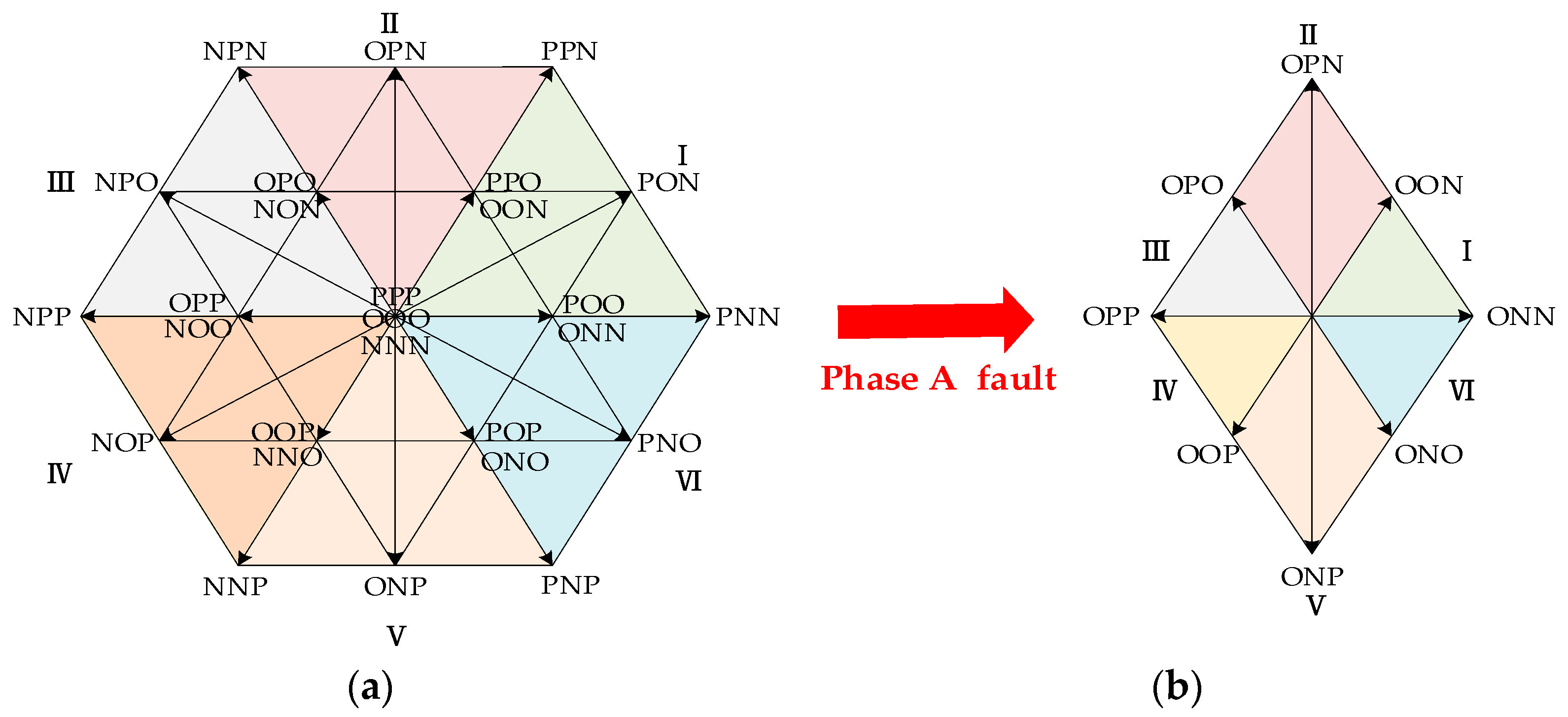
2. ESTPI Fault Topology and Mechanism of NPP Fluctuation

2.1. The Space Voltage Vector of ESTPI Topology

This work discusses the fault-tolerant topology of three-level NPC inverters, which is shown in Figure 1. The system comprises a DC-link voltage (Vdc), as well as two capacitors C1 and C2, whose voltages are up and un, respectively. Point O denotes the neutral point of the DC bus, and ila, ilb, and ilc are the output currents of three-level NPC inverters. For three-level NPC inverters, there are four power semiconductor devices (Sx1, Sx2, Sx3, Sx4), two clamped diodes, a bidirectional thyristor (T1, T2, T3) and two fast-acting fuses (FU) on each phase bridge arm.
Due to the three-phase symmetry, only phase A faults are analysed as an example. As shown in Figure 1, when phase A fails, the fast-acting fuse on phase A is disconnected, and the bidirectional thyristor on phase A is activated, thus, the output current of phase A is the NP current of the DC bus. The other two normal arms of ESTPI have three states, including P, O, and N. The switching function is defined as follows:
S x = { 1 ( P ) , S x 1 , S x 2   o n , S x 3 , S x 4   o f f 0 ( O ) , S x 2 , S x 3   o n , S x 1 , S x 4   o f f 1 ( N ) , S x 3 , S x 4   o n , S x 1 , S x 2   o f f ( x = a , b , c )
Due to phase A failure, it can only output O state. The operating modes of the three-phase three-level NPC inverters have 27 combinations, the failure of phase A restricts it to only nine combinations, as shown in Figure 2. In Figure 2b, the ESTPI topology space vector diagram can be divided into six sectors, labelled as I to VI. Sectors II and V contain medium voltage vectors that can be further divided into two subsectors. The overall space voltage vector distribution still satisfies the synthesis conditions of the reference voltage vector.
Due to the change in space voltage vector distribution, there are only nine available vectors to ensure the operation of ESTPI, the reference voltage synthesis method must be redesigned. To minimize the low-frequency oscillation caused by the CMV, it is necessary to analyse the CMV generated by each voltage vector.
The output voltage of the ESTPI can be obtained as follows:
{ u a o = 0 u b o = S b × V d c 2 u c o = S c × V d c 2
where Sb, Sc are defined by Formula (1). The CMV is expressed as follows:
u c m = u a o + u b o + u c o 3
From Formulas (1)–(3), the CMV of each basic voltage vector is shown in Table 1.
As indicated in Table 1, small voltage vectors will generate the CMV, and the CMV of zero voltage vector and medium voltage vectors are zero. Traditional SVPWM relies solely on small voltage vectors to synthesize reference voltage vectors for ESTPI, so the CMV is great. In this paper, the medium voltage vectors in sectors II and V are incorporated into the synthesis of reference voltage vectors to reduce CMV. This approach of introducing medium voltage vectors effectively reduces the proportion of the small voltage vectors in the reference voltage vector synthesis, ultimately leading to the decrease in CMV.
In order to optimize computational efficiency, the synthesis of the reference voltage vector and the calculation of the duration time of the voltage vector are executed within the 60° (g-h) coordinate systems. In sector I, the duration time can be computed by the following means.
In Figure 3, Vref is the reference voltage vector synthesized by V0, V1, and V2, a1 is the equivalent vector of V2 with duration t2 in one modulation cycle. b1 is the equivalent vector of V1 with duration t1 in one modulation cycle. The modulation index is defined as follows:
m = 3 × V r e f V d c
The vector duration time t1 and t2 can be obtained as follows:
{ b 1 = V 1 × t 1 T s V 1 = V d c / 3 a = V r e f × sin ( π 3 θ ) a / b 1 = cos ( π 6 ) t 1 = b 1 T s V 1 = a T s V 1 × cos ( π 6 ) = 2 T s V r e f × sin ( π 3 θ ) 3 × V d c 3 = 2 m T s sin ( π 3 θ )
{ a 1 = V 2 × t 2 T s V 2 = V d c / 3 b = V r e f × sin ( θ ) b / a 1 = sin ( π 3 ) t 2 = a 1 T s V 2 = b T s V 2 × sin ( π 3 ) = 2 T s V r e f × sin ( θ ) 3 × V d c 3 = 2 m T s sin ( θ )
The calculation of the vector duration time of other sectors is similar. The vector duration time and the synthesis rules for reference voltage are shown in Table 2 and Table 3.

2.2. The NPP Fluctuant Mechanism of DC Bus

According to Table 2 and Table 3, it is possible to obtain synthesis rules for the reference voltage vector. Therefore, the NP current during one fundamental period can be analysed. Assuming three-phase symmetry,
{ i l a = I m cos ( θ φ ) i l b = I m cos ( θ φ 2 π 3 ) i l c = I m cos ( θ φ + 2 π 3 )
where ila, ilb, and ilc are the output current of ESTPI, Im, and φ denotes the amplitude of the phase current and the power factor angle, respectively. Due to the modulation period being short, it is assumed that the current remains constant in a modulation period. Moreover, since the NP current is not affected by the zero voltage vector, the NP current during each modulation period can be represented by the NP current with V1 and V2. The principle of area equivalence is expressed as follows:
i o × T s = i o 1 × t 1 + i o 2 × t 2
where io, TS are the NP current of the DC bus and the modulation period, respectively. io1, io2 are the corresponding NP current with V1 and V2. t1, t2 are the duration time of V1 and V2, respectively. io1, io2, t1 and t2 can be obtained in Table 2.
Combine Table 2, Formulas (7) and (8), the NP current of the DC bus is expressed as follows:
i o = { 3 m I m cos φ 0 θ < π 3 , ( Sector   I ) m I m [ 2 sin ( 2 θ φ ) sin ( φ ) ]       π 3 θ < π 2 ,   ( Sector   II ) m I m [ 2 sin ( 2 θ φ ) sin ( φ ) ]       π 2 θ < 2 π 3 , ( Sector   II ) 3 m I m cos ( φ )           2 π 3 θ < π ,   ( Sector   III ) 3 m I m cos ( φ )           π θ < 4 π 3 ,   ( Sector   IV ) m I m [ 2 sin ( 2 θ φ ) sin ( φ ) ] 4 π 3 θ < 3 π 2 , ( Sector   V ) m I m [ 2 sin ( 2 θ φ ) sin ( φ ) ] 3 π 2 θ < 5 π 3 , ( Sector   V ) 3 m I m cos ( φ )         5 π 3 θ 2 π , ( Sector   VI )
Formula (9) shows that the NP current has half-wave symmetry, that is i o ( θ ) = i o ( θ + π ) . This means that the average value of NP current is zero during one fundamental cycle, and the NPP of the DC bus can remain balance. Further, by using Fourier decomposition on Formula (9) can obtain:
{ a 0 = 0 a 1 = m I m 16 + 384 cos 2 ( φ ) 3 π a 2 = 0 a 3 = 8 3 m I m cos ( φ ) 3 π
where a0, a1, a2, and a3 correspond to the DC component, the fundamental component, the second harmonic component, and the third harmonic component, respectively. As shown in Formula (10), the NP current only contains odd harmonic waves. Thus, the NPP variation can be succinctly expressed as follows:
Δ u V d c = ( u p u n ) 2 V d c = i o d t V d c × 2 C         = 2 m I m 1 + 24 cos 2 ( φ ) V r e f 3 π C ω sin ( ω t ζ 1 ) + n = 3 , 5 , 7 A n 2 V d c C n ω sin ( n ω t ζ n )
where Δ u = ( u p u n ) 2 is the NPP fluctuation of the DC bus, and ζ n (n = 3, 5, 7 …) is the initial phase of the NPP corresponding to the nth harmonic current. C is the DC-link capacitance, and An is the nth harmonic current component. Combined with Formulas (9) and (11), under the condition of ESTPI, it can be seen that the NPP of the DC bus fluctuates with the fundamental wave frequency. The fluctuation primarily stems from the capacitance of the DC-link capacitor, as well as the amplitude and phase of the grid-connected currents, and modulation depth.

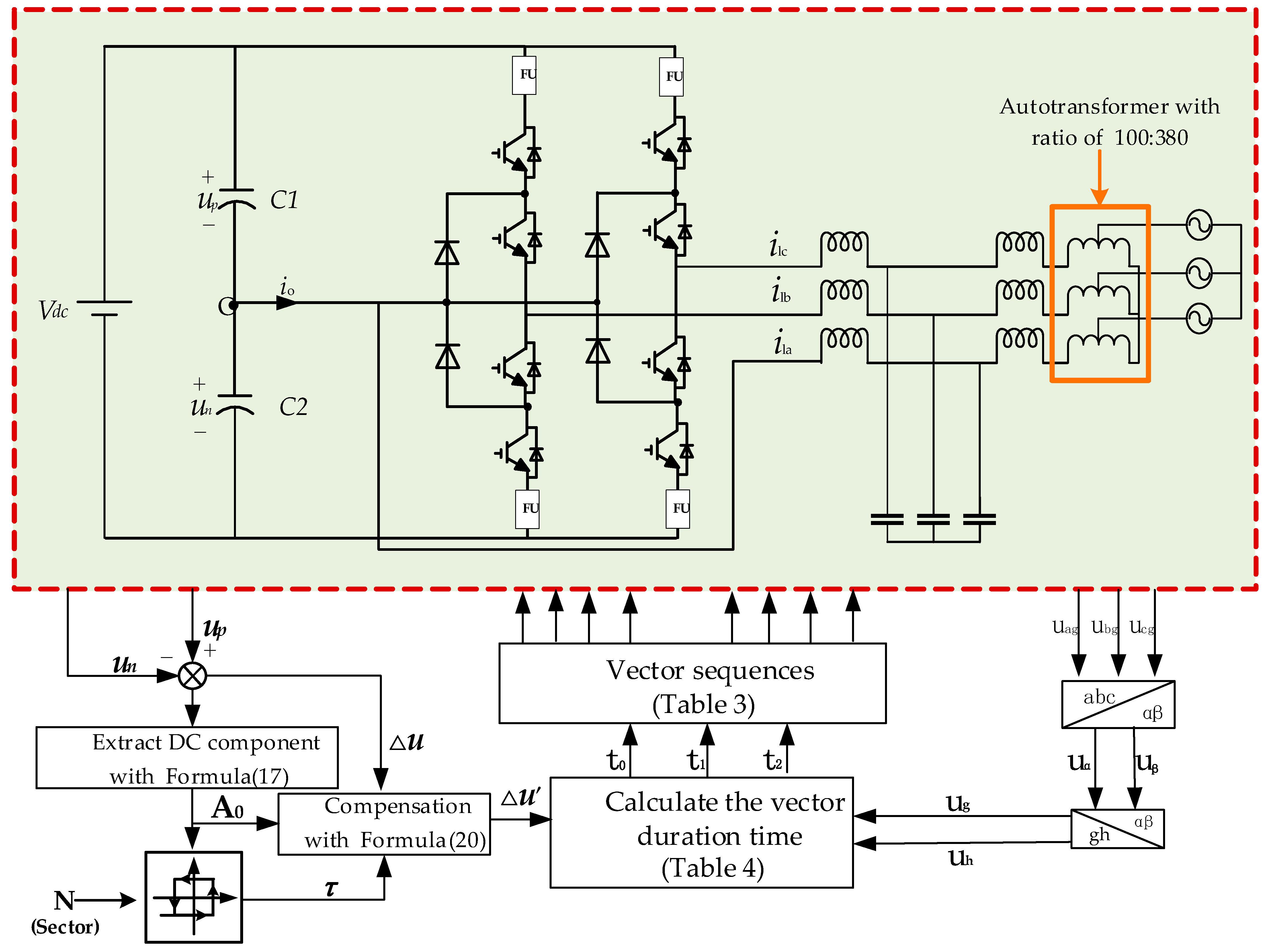
3. SVPWM Compensation and Optimization

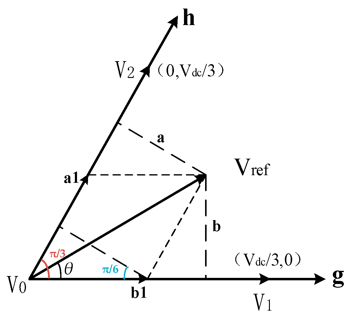
3.1. SVPWM Compensation Strategy Considering NPP Fluctuation

By analysing the output level status of the ESTPI, the ESTPI output voltage considering the fluctuation of the NPP can be obtained as follows:
{ u a o = 0 u b o = S b × V d c 2 + | S b | × Δ u u c o = S c × V d c 2 + | S c | × Δ u
where, uao, ubo, and uco are the ESTPI output voltages of phases A, B, and C, respectively. Δ u is the NPP fluctuation of the DC bus. Therefore, the space voltage vector is expressed as follows:
u s = 2 3 ( u a o + u b o e j 2 3 π + u c o e - j 2 3 π )
The basic voltage vectors coordinate considering NPP fluctuation can be obtained by combining Formulas (1), (12) and (13), as shown in Table 4.
As can be seen in Table 4 and Figure 4, it is clear that the NPP fluctuation will result in an uneven distribution of space voltage vectors, which will cause imbalances of ESTPI output. This will affect the grid-connected power quality and narrow the linear modulation area, and the NPP fluctuation is an inherent phenomenon. Unfortunately, there are no redundant vectors available for NPP control in ESTPI. Imbalance of ESTPI output is inevitable.
It is obvious that the NPP fluctuation of the DC bus will change the distribution of basic voltage vectors. If the method in Table 2 is still used to synthesize the reference voltage vector, the grid-connected power quality will deteriorate. At the same time, choosing the DC-link capacitor’s capacity according to the lowest limitation is a common cost-saving measure in practical industrial applications, which will worsen the fluctuation of NPP and further deteriorate the power quality. Therefore, it is necessary to consider the impact of NPP fluctuation on the synthesis of the reference voltage vector. Based on the volt-second balancing principle, the reference voltage vector synthesis should be compensated when the NPP fluctuates.
The duration time of the fundamental vector is recalculated considering NPP fluctuation. The calculation method remains the same as presented in Formulas (5) and (6), with the exception that the vector coordinates need to incorporate variations in NPP. The reference voltage vector synthesis rules are outlined in Table 5.
To examine the compensation effect of reference voltage vector synthesis considering the NPP fluctuation, the grid-connected currents and voltages of the DC-link capacitors are tested. The main circuit parameters are shown in Table 6, with the grid-connected currents at 6A and the capacitances of the DC-link are 820 μF. The simulation results are illustrated in Figure 5.
As shown in Figure 5a, if the NPP fluctuation is not considered in the synthesis of the reference voltage vector, the NPP fluctuation can remain balanced, but the distortion of the grid-connected currents is severe. As shown in Figure 5b, when NPP fluctuation is taken into account in the synthesis of the reference voltage vector, the grid-connected currents have good sine waves at the beginning, but the NPP gradually deviates from the equilibrium point until exceeding the linear modulation region. Then, the reference voltage vector no longer satisfies the principle of volt-second balancing and results in a serious distortion of the grid-connected currents. In summary, considering the NPP fluctuation can improve the quality of three-phase grid-connected currents at the beginning, but NPP will still deviate from the equilibrium point. Thus, it is necessary to investigate the reasons for the NPP fluctuation increasing and optimize the compensation of the space vector modulation.

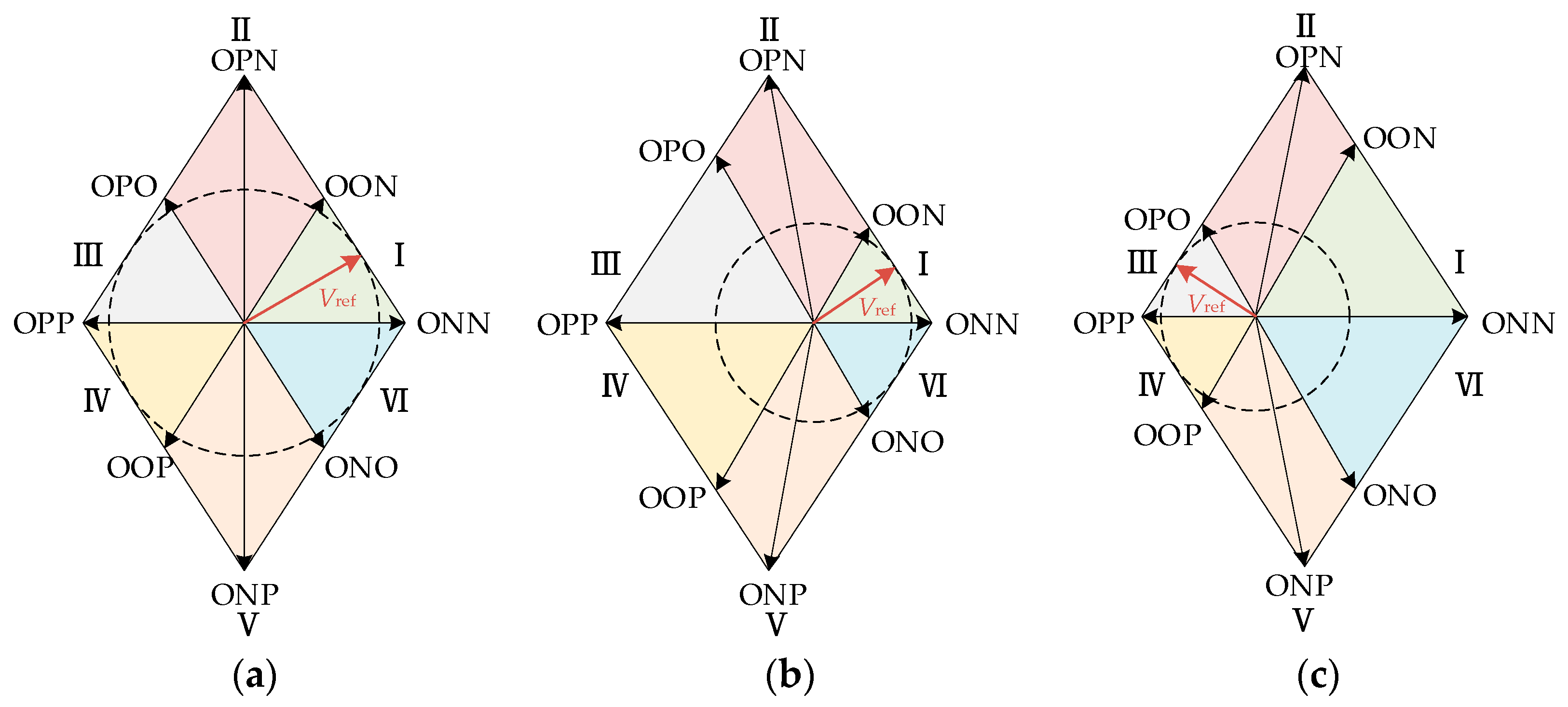
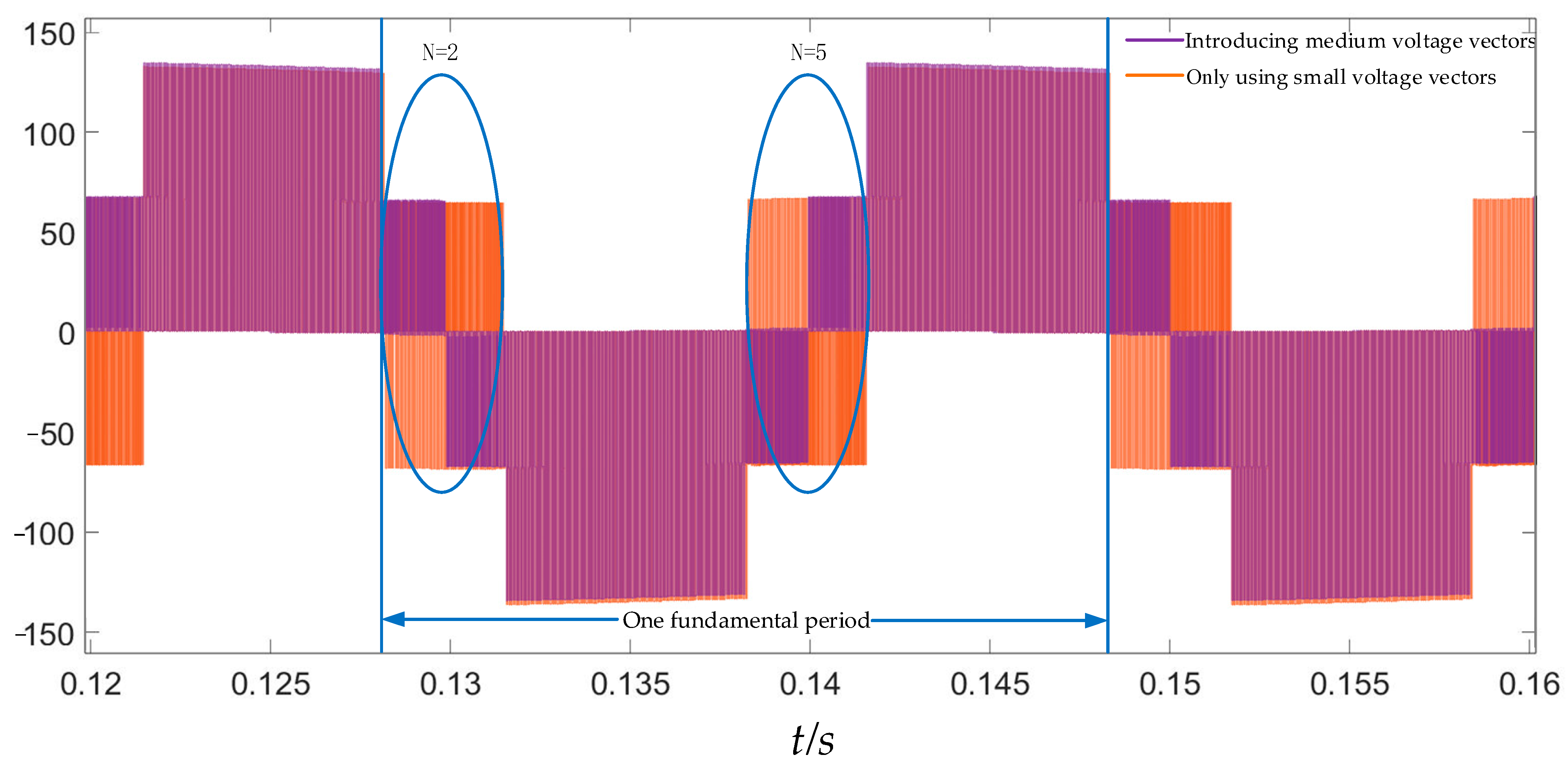
3.2. Optimization of SVPWM

To ensure the inverter is still running and providing power to the grid after the single bridge arm fault, it is necessary to find the reasons for the NPP’s significant fluctuation, then design the effective control strategy. Combine Table 5, Formulas (5) and (6), and the NP current of the DC bus with NPP fluctuation can be expressed as Formula (14):
i o = { 3 m I m cos φ ( 1 2 Δ u / V d c ) 0 θ < π 3 , ( Sector   I ) K 21 × ( I m cos ( θ φ + 2 π 3 ) - I m cos ( θ φ ) × 2 m sin ( π / 3 θ ) ( 1 + 2 Δ u / V d c )           π 3 θ < π 2 , ( Sector   II ) K 22 × ( I m cos ( θ φ 2 π 3 ) + I m cos ( θ φ ) × 2 m sin ( π / 3 + θ ) ( 1 2 Δ u / V d c )           π 2 θ < 2 π 3 ,   ( Sector   II ) 3 m I m cos φ ( 1 + 2 Δ u / V d c )       2 π 3 θ < π , ( Sector   III )   3 m I m cos φ ( 1 + 2 Δ u / V d c )       π θ < 4 π 3 , ( Sector   IV ) K 51 × ( I m cos ( θ φ + 2 π 3 ) + I m cos ( θ φ ) × 2 m sin ( π / 3 θ ) ( 1 2 Δ u / V d c )           4 π 3 θ < 3 π 2 ,   ( Sector   V ) K 52 × ( I m cos ( θ φ 2 π 3 ) I m cos ( θ φ ) × 2 m sin ( π / 3 + θ ) ( 1 + 2 Δ u / V d c )           3 π 2 θ < 5 π 3 , ( Sector   V )   3 m I m cos φ ( 1 2 Δ u / V d c )       5 π 3 θ 2 π , ( Sector   VI )  
where, K21, K22, K51, K52 are defined as Formula (15).
{ K 21 = 2 m sin ( π / 3 + θ ) / ( 1 2 Δ u / V d c ) + 2 m sin ( π / 3 θ ) / ( 1 + 2 Δ u / V d c ) K 22 = 2 m sin ( π / 3 θ ) / ( 1 + 2 Δ u / V d c ) 2 m sin ( π / 3 + θ ) / ( 1 2 Δ u / V d c ) K 51 = 2 m sin ( π / 3 + θ ) / ( 1 + 2 Δ u / V d c ) 2 m sin ( π / 3 θ ) / ( 1 2 Δ u / V d c ) K 52 = 2 m sin ( π / 3 θ ) / ( 1 2 Δ u / V d c ) + 2 m sin ( π / 3 + θ ) / ( 1 + 2 Δ u / V d c )
Comparing Formulas (9) and (14), it is evident that the addition of compensation (Δu/Vdc) causes the NP current to no longer satisfy the half-wave symmetry in Formula (14). Therefore, the NPP of the DC bus deviates from the equilibrium point. To maintain Formula (14) to satisfy i o ( θ ) + i o ( θ + π ) = 0 , the following relationship should be maintained, as shown in Formula (16):
Δ u ( θ ) / V d c + Δ u ( θ + π ) / V d c = 0  
For Equation (16) to hold true, the voltage deviation of the DC link (Δu) should not contain the DC component. Thus, the space vector modulation of adding the NPP fluctuation should be further refined.
To eliminate the DC component of Δu, the DC component should be extracted first. A first-order low-pass filter is designed to obtain the DC component in this work. In the s-domain, the first-order low-pass filter can be expressed as follows:
G ( s ) = 1 1 + s / ω c
where ωc is its cutoff frequency. According to Formula (11), it can be seen that the main AC component in the NPP fluctuation of the DC bus is the fundamental component with an angular frequency of approximately 314 rad/s. To extract the DC component, the cutoff frequency of the low-pass filter must be lower than the fundamental angular frequency. According to low-pass filter phase-frequency characteristics, when the signal passes through the filter, a large phase shift will be generated at a lower cutoff frequency, which will affect the filtering accuracy of the DC component. In this paper, the cutoff frequency is selected as 80 rad/s.
To prevent the DC bus NPP from deviating too much from the equilibrium point, a hysteresis comparator is designed to further adjust the space vector modulation compensation. The NP current is obtained by Formula (18):
i o = { 3 m I m cos φ / ( 1 2 Δ u / V d c )       sector   I ,   VI 3 m I m cos φ / ( 1 + 2 Δ u / V d c )   sector   III ,   IV
According to Formula (18), in sector I, III, IV, and VI, if the value of the grid-connection system parameters (Im and φ) is determined, 3 m I m cos φ can be considered as a constant, and cosφ is greater than or equal to 0 within a range of φ between −90° and 90°. According to Formulas (11) and (18), NPP fluctuation can be controlled by adjusting the compensation value of the reference voltage vector synthesis in sectors I, III, IV and VI. However, it is important to note that the modulation can be considered as a proportional link throughout the entire grid-connected control, and Vref is the output of the grid-connected controller that converts into the switch driver signal via space vector modulation. Consequently, the hysteresis comparator is designed to adjust the compensation value, only when the NPP of the DC bus contains the DC component and deviates large enough from the equilibrium point, the hysteresis comparator will compensate the voltage vector. The compensation value in Formula (18) is adjusted to prevent the NPP of the DC bus from deviating from the equilibrium point, achieving the synthesis of the reference voltage vector lying in the linear modulation region.
Given 0.5 u max Δ u u max , the output of the hysteresis comparator should be a suitable value that can compensate for the NPP fluctuation, otherwise 0, umax is the maximum allowable voltage of NPP fluctuation in the linear modulation area. Since the DC component increases as the NPP deviates from the equilibrium point, the output of the hysteresis comparator also increases, and more robust control of the NPP of the DC bus can be realised. Therefore, the output of the hysteresis comparator can be designed according to the DC component of NPP fluctuation, which can be represented as follows:
τ = K × sgn ( A 0 ) sector   I ,   III ,   IV ,   VI
where, K = |A0|+1, A0 is the DC component of NPP fluctuation.
In conclusion, the optimised compensation value is shown in Formula (20):
Δ u = Δ u A 0 + τ = u p u n 2 A 0 + τ
Based on the above analysis, a fault-tolerant control strategy with SVPWM compensation optimisation is constructed, as shown in Figure 6.

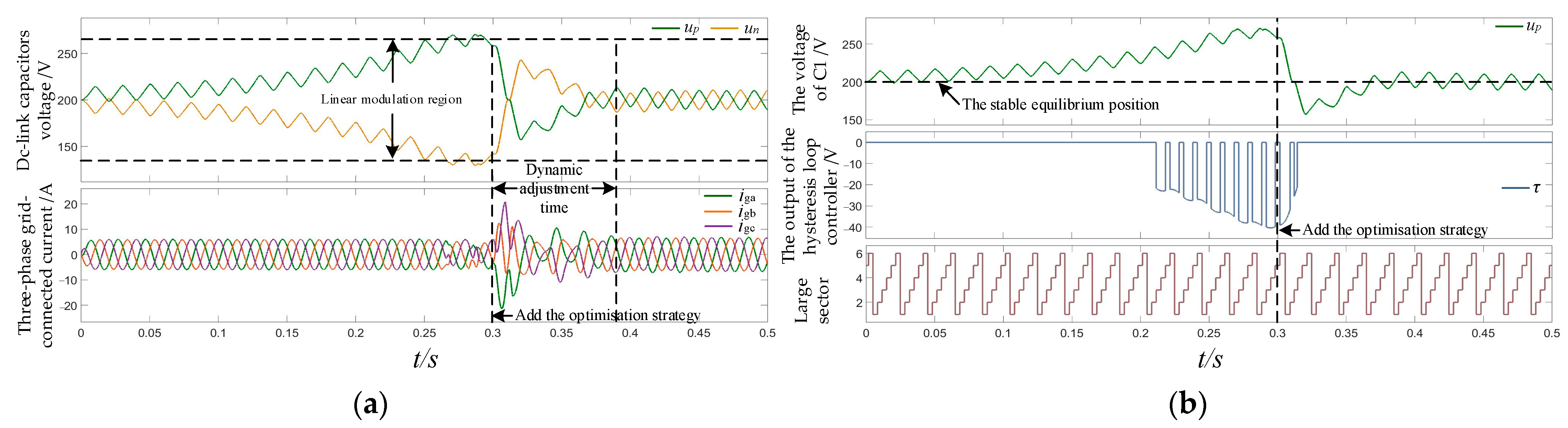
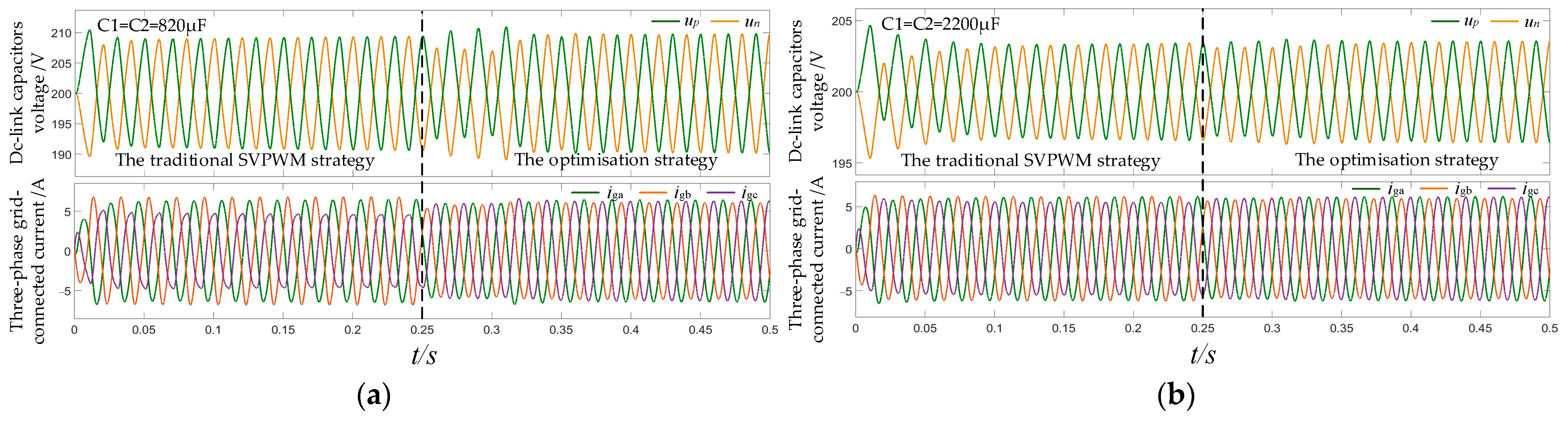
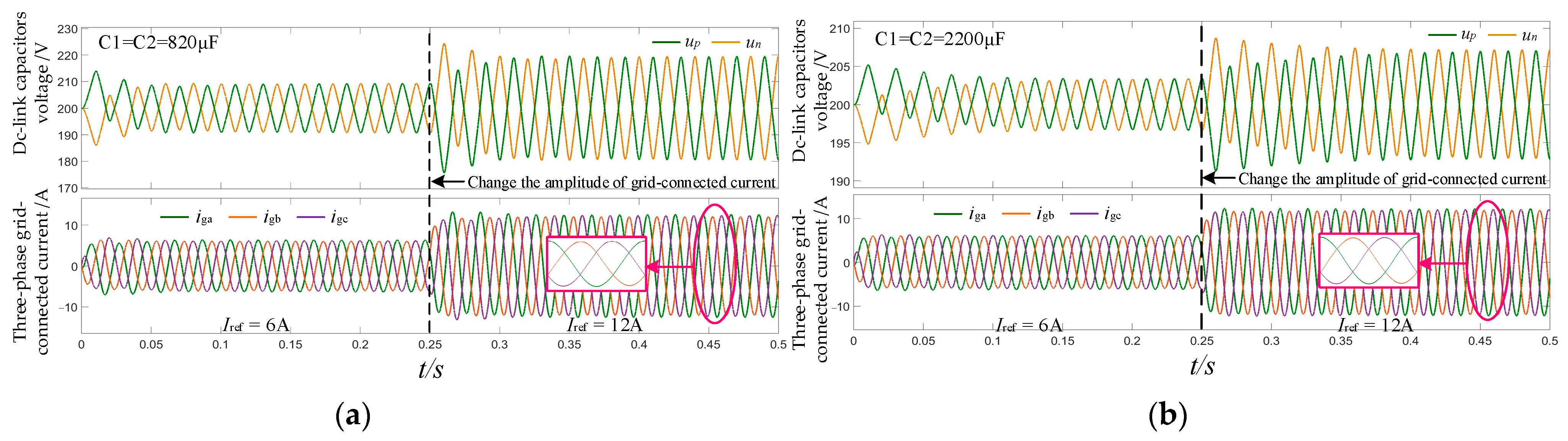
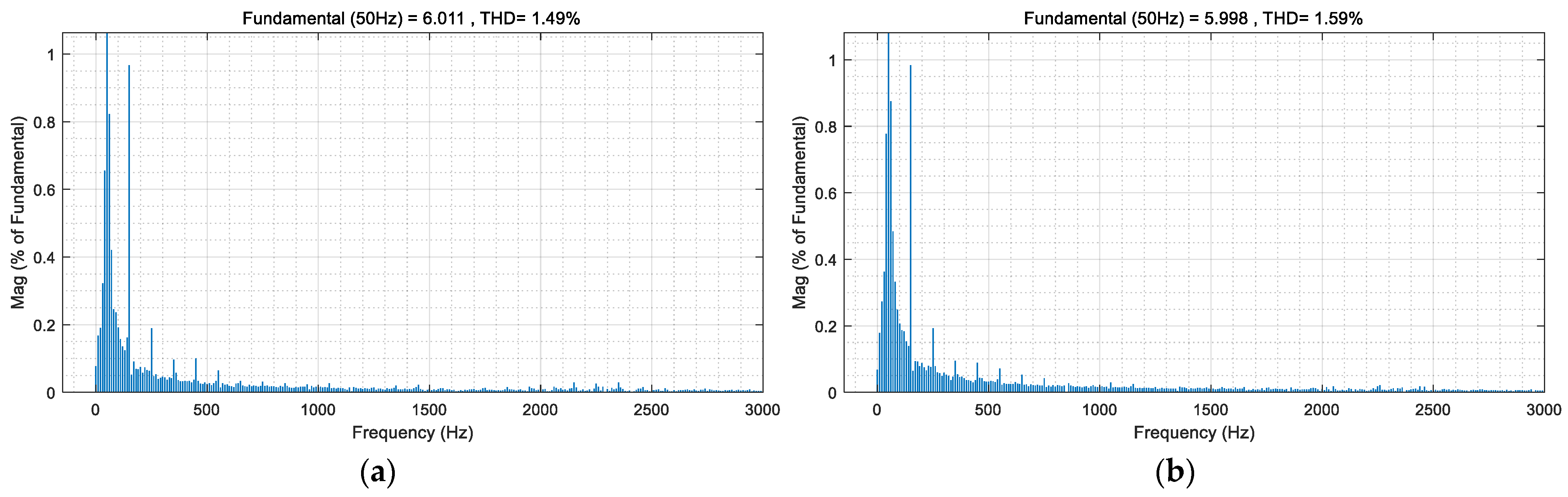
4. Simulation and Results Analysis

To verify the effect of the fault-tolerant control strategy proposed in this paper, a three-level NPC grid-connected inverter experimental device is simulated and analysed using MATLAB/Simulink. The topology of postfault three-phase three-level NPC grid-connected inverters is shown in Figure 7. The LCL filter in the rear stage of the inverter connects to the power grid through the autotransformer and isolation transformer. The ratio of the autotransformer is 100:380. The main parameters of the inverter are shown in Table 6.
To verify the effectiveness of the proposed strategy, the simulation is carried out as follows. The system runs with the control strategy of considering NPP fluctuation not extracting the DC component at the beginning, and NPP will deviate from the balance. When NPP exceeds the linear modulation region, the grid-connection current will distort severely. At this time, the proposed strategy is applied to the system to confirm the suppression effect on the NPP fluctuation. In this way, the grid-connected currents are compared between the traditional SVPWM and our proposed optimized strategy. To verify the performance when the load changes, the simulation is carried out with a grid-connected current step from 6A to 12A. Finally, the improvement in CMV is verified by comparing the proposed method with the traditional SVPWM method.

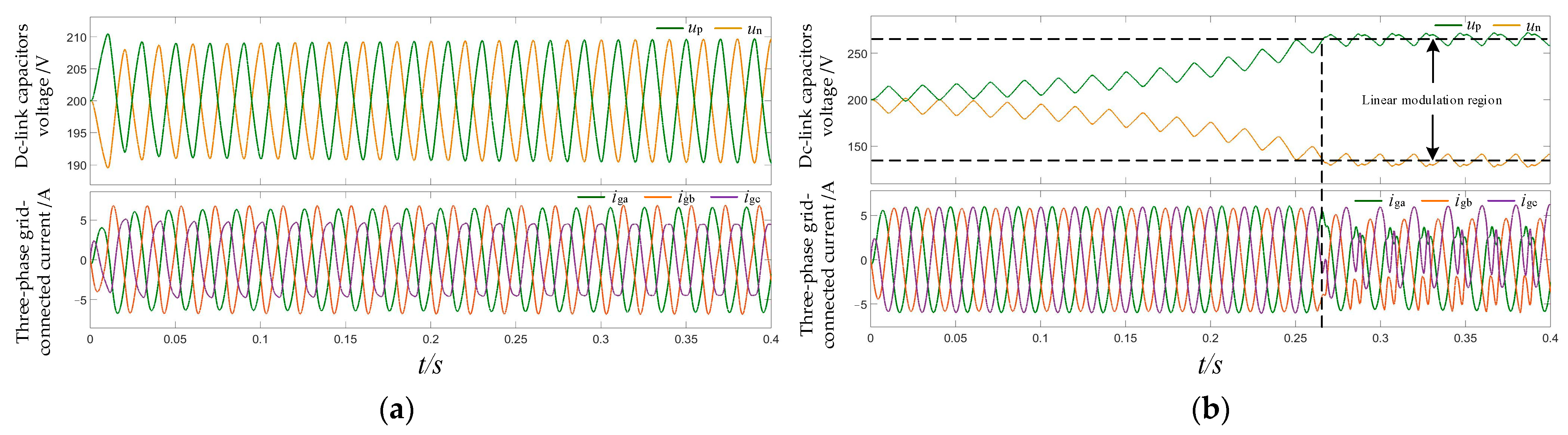
4.1. The Compensation Optimization Strategy Control Effect

Firstly, the correctness of the fault-tolerant control strategy proposed is verified. The grid-connection currents are 6A and the capacitances of DC-link are 820 μF. To evaluate the compensation optimisation strategy, the grid-connected currents and DC-link capacitors’ voltage are tested, respectively. Figure 8 displays the simulation results.
In Figure 8a, iga, igb, and igc are the three-phase grid-connected currents. If the SVPWM is not optimised, the grid-connected currents experience significant distortion over time due to the DC bus NPP deviating from the equilibrium point. Even if the sine waves of grid-connected currents are good at first, they will distort when Vref exceeds the linear modulation range. However, by implementing the SVPWM compensation optimisation strategy at 0.3 s, the NPP of the DC bus can be effectively controlled. The NPP and grid-connected currents tend to be stable at 0.39 s. The dynamic processing is less than 0.1 s and the quality of grid-connected currents have noticeable improvement.
Figure 8b shows the increase output of the hysteresis comparator with the increasing of NPP deviation. When the SVPWM compensation optimisation strategy is applied at 0.3 s, the reference voltage vector is in sector V this moment. The output of hysteresis comparator is zero and has no effect on the control loop. When the reference voltage vector changes to sector VI, the NPP decreases rapidly due to the proposed strategy, then the output of the hysteresis comparator returns to zero when the NPP deviation is less than 20 V.
According to Formula (11), there is a correlation between NPP fluctuation and the DC bus’s capacitance. To verify the control ability of the fault-tolerant control strategy with different capacitances, capacitances of 820 μF and 2200 μF are tested, respectively. The simulation involved both traditional SVPWM and the proposed SVPWM compensation optimisation strategy, and the results are shown in Figure 9.
As shown in Figure 9, as the capacitance increases from 820 μF to 2200 μF, the voltage fluctuation of the DC bus capacitor and the distortion of the grid-connected currents decrease. The currents behave distortion significantly with traditional SVPWM, especially when the capacitance is small (820 μF). At 0.25 s, the SVPWM compensation optimisation strategy is applied in both capacitance cases, and the degree of grid-connected current distortion gets improvement drastically. When the DC-link capacitance is 820 μF, the total harmonic content analysis (THD) of the grid-connected currents before and after the SVPWM compensation optimisation strategy are shown in Figure 10.
As shown in Figure 10, when the DC-link capacitances are 820 μF, we can see a remarkable reduction in the THD of the grid-connected currents from 10.41% to 2.03% by implementing the SVPWM compensation optimisation strategy. This improvement significantly enhances the quality of the grid-connected currents, meeting the requirement for grid connection (THD ≤ 5%). These findings indicate that even when the capacitances of the DC-link are small, the compensation optimisation strategy can effectively compensate the grid-connected currents, the hardware costs and volume can be reduced.
To further validate the efficacy of the compensation optimization strategy when the grid-connected power changes, the simulations are carried out with the amplitude of grid-connected currents varying from 6 A to 12 A. As shown in Figure 11, when the grid-connected currents increase, the NPP fluctuation also increases, which is consistent with the theoretical analysis in Formula (11). The grid-connected currents remain in the form of smooth sine waves, despite abrupt change in the amplitude of grid-connected currents.
In Figure 11a, the NPP deviation amplitude is greater than that in Figure 11b, as described in Formula (11). When the amplitude of the grid-connected currents changes suddenly, the half-wave symmetry of the NP current is destroyed in a fundamental period, leading to the NPP fluctuation containing the DC component. Therefore, the NPP and the grid-connected currents need to be dynamically adjusted to restore balance. When the DC bus capacitances are 2200 μF, the maximum rms deviation percentage of steady-state three-phase grid-connected currents is 2.66%. When DC bus capacitances are 820 μF, the maximum rms deviation percentage of the steady-state three-phase grid-connected currents is 4.33%. In both situations, the maximum rms deviation percentage of steady-state three-phase grid-connected currents are relatively small. When the amplitude of the grid-connected currents changes and the DC bus capacitances are 820 μF, the maximum NPP fluctuation is 24 V, and the maximum DC bus NPP deviation tolerated within the linear modulation region is 63 V. Despite the NPP’s significant fluctuation amplitude under these conditions, the ESTPI can operate properly. Thus, the SVPWM compensation optimisation strategy designed in this paper can ensure the continuous operation of the three-level NPC inverter after a single-arm failure.

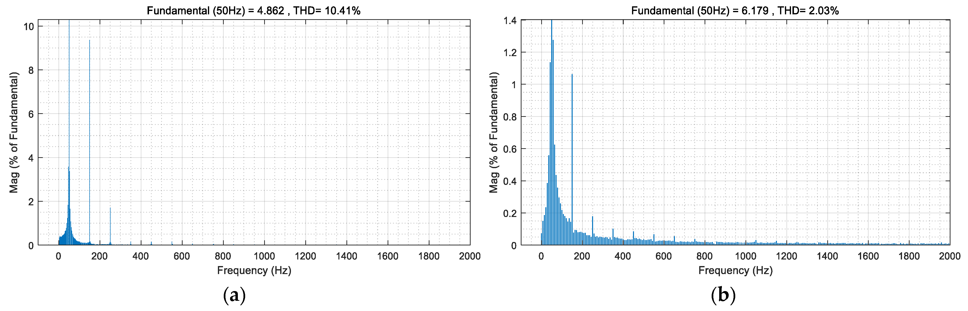
4.2. The Improvement of Common Mode Voltage

In the SVPWM compensation optimization strategy, the medium vector is employed for the space vector synthesis in sector II and V. This results in reduction in the proportion of the small vector, leading to a decrease in the CMV. To evaluate the impact of the approach, the THD of the currents with the vector synthesis method only using small vectors and introducing medium vectors are analysed, respectively, and the results are shown in Figure 12.
According to the data presented in Figure 12, when introducing medium vectors in vector synthesis, the THD of grid-connected currents is 1.59%, which is slightly higher than the 1.49% only using small vectors. This is because the switch sequence is unable to meet the three-phase symmetry requirement within one-third of one fundamental period when incorporating medium vectors. Thus, the content of the third harmonic and its multiples harmonics of the ESTPI output currents will increase. The THD of grid-connected currents is still less than 5% in both cases, with only a 0.10% difference between the two methods, but the vector synthesis method introducing medium vectors can effectively reduce CMV. As shown in Figure 13:
The method with the medium-voltage vector is used to synthesize the reference voltage vector. When the reference voltage vector is in subsector 1 of sector II, the CMV changes from −Vdc/6 to 0, the CMV changes from Vdc/6 to 0 in subsector 2. When the reference voltage vector is in subsector 1 of sector V, the CMV changes from Vdc/6 to 0, and the CMV changes from −Vdc/6 to 0 in subsector 2. This indicates that the proposed fault-tolerant control strategy not only can guarantee exceptional grid-connection control after a single-arm fault, but also can significantly reduce the CMV for one-third of the time within each fundamental wave period, with the CMV decreasing accordingly throughout the entire cycle, which is conducive to grid-connection operation.

5. Conclusions

This paper proposed a fault-tolerant control strategy for three-level NPC grid-connected inverters based on SVPWM. First, after the single-arm of the NPC grid-connected inverter failure, the CMV is improved by repartitioning the sectors and subsectors and selects a new reference voltage vector synthesis sequence. Then, based on the NPP migration mechanism of the DC bus, the low-pass filter and hysteresis controller are designed to optimise and compensate for the reference voltage vector synthesis, which can restrict the reference voltage vector in the linear modulation area. The optimised SVPWM algorithm can effectively suppress NPP migration and improve the quality of grid-connected currents. When the amplitude of the grid-connected currents suddenly changes, the improved fault-tolerant control strategy can also realise the three-phase balance of the inverter output and maintain good grid-connected power quality.
With the proposed fault-tolerant control strategy, the THD of grid-connected currents decreases from 10.41% to 2.03%, and the amplitude of CMV decreases in one-third of one fundamental period. The simulation results verify the effectiveness of the proposed fault-tolerant control strategy and provide a guarantee for the continuous stable operation of the three-level NPC grid-connected inverters after a single-arm fault.

Author Contributions

Conceptualization, J.H.; formal analysis, J.H.; funding acquisition, J.H.; investigation, F.B.; methodology, J.H. and F.B.; project administration, J.H.; software, Q.Y.; validation, Q.Y. and S.R.; visualization, F.B. and S.R.; writing—original draft, F.B.; writing—review and editing, J.H. and Q.Y. All authors have read and agreed to the published version of the manuscript.

Funding

This research was funded by National Natural Science Foundation of China (U1504617) and University-Industry Collaborative Education Program, China (202101222007).

Data Availability Statement

Data are contained within the article.

Conflicts of Interest

The authors declare no conflict of interest.

References

  1. Nabae, A.; Takahashi, I.; Akagi, H. A New Neutral-Point-Clamped PWM Inverter. IEEE Trans. Ind. Appl. 1981, IA-17, 518–523. [Google Scholar] [CrossRef]
  2. Rodriguez, J.; Bernet, S.; Steimer, P.K.; Lizama, I.E. A Survey on Neutral-Point-Clamped Inverters. IEEE Trans. Ind. Electron. 2010, 57, 2219–2230. [Google Scholar] [CrossRef]
  3. Choi, U.-M.; Lee, J.-S.; Blaabjerg, F.; Lee, K.-B. Open-Circuit Fault Diagnosis and Fault-Tolerant Control for a Grid-Connected NPC Inverter. IEEE Trans. Power Electron. 2015, 31, 7234–7247. [Google Scholar] [CrossRef]
  4. Chao, K.-H.; Ke, C.-H. Fault Diagnosis and Tolerant Control of Three-Level Neutral-Point Clamped Inverters in Motor Drives. Energies 2020, 13, 6302. [Google Scholar] [CrossRef]
  5. Yang, C.; Peng, T.; Yang, C.; Karimi, H.R.; Ding, X. Voltage Difference Residual-Based Open-Circuit Fault Diagnosis Approach for Three-Level Converters in Electric Traction Systems. IEEE Trans. Power Electron. 2020, 35, 3012–3028. [Google Scholar] [CrossRef]
  6. Fayyaz, M.M.; Syed, I.M.; Meng, Y.; Aman, M.N. Comprehensive Predictive Control Model for a Three-Phase Four-Legged Inverter. Energies 2023, 16, 2650. [Google Scholar] [CrossRef]
  7. Zhou, D.; Zhao, J.; Liu, Y. Finite-control-set model predictive control scheme of three-phase four-leg back-to-back converter-fed induction motor drive. IET Electr. Power Appl. 2017, 11, 761–767. [Google Scholar] [CrossRef]
  8. Zhang, W.; Xu, D. Fault Analysis and Fault-Tolerant Design for Parallel Redundant Inverter Systems in Case of IGBT Short-Circuit Failures. IEEE J. Emerg. Sel. Top. Power Electron. 2018, 6, 2031–2041. [Google Scholar] [CrossRef]
  9. Yu, Y.; Li, X.; Wei, L. Fault Tolerant Control of Five-Level Inverter Based on Redundancy Space Vector Optimization and Topology Reconfigruation. IEEE Access 2020, 8, 194342–194350. [Google Scholar] [CrossRef]
  10. Xu, S.Z.; Wang, C.J.; Wang, Y. An Improved Fault-Tolerant Control Strategy for High-Power ANPC Three-Level Inverter Under Short-Circuit Fault of Power Devices. IEEE Access 2019, 7, 55443–55457. [Google Scholar] [CrossRef]
  11. Azer, P.; Ouni, S.; Narimani, M. A Novel Fault-Tolerant Technique for Active-Neutral-Point-Clamped Inverter Using Carrier-Based PWM. IEEE Trans. Ind. Electron. 2020, 67, 1792–1803. [Google Scholar] [CrossRef]
  12. Liu, Y.C.; Ge, X.; Tang, Q. Relationship between Two Different Space-Vector Modulation Methods of Eight-Switch Three-Phase Inverters. In Proceedings of the 2016 IEEE 8th International Power Electronics and Motion Control Conference (IPEMC-ECCE Asia), Hefei, China, 22–26 May 2016; pp. 3206–3210. [Google Scholar] [CrossRef]
  13. Zhang, M.; Li, Z.; Guo, Y.; Zhang, X. Fault Tolerance and Overmodulation Algorithm for Three Level Neutral Point Clamped Inverters. In Proceedings of the 36th Chinese Control Conference (CCC), Dalian, China, 26–28 July 2017; pp. 7358–7363. [Google Scholar] [CrossRef]
  14. An, S.-W.; Kim, S.-M.; Lee, K.-B. Optimized Space-Vector Modulation to Reduce Neutral Point Current for Extending Capacitor Lifetime in Three-Level Inverters. IEEE Access 2020, 8, 97689–97697. [Google Scholar] [CrossRef]
  15. Liu, Z.; Zhang, W.; Li, C.; Wang, X.; Qin, H. Improved virtual SVPWM algorithm for CMV reduction and NPV oscillation elimination in Three-Level NPC inverter. Int. J. Electr. Power Energy Syst. 2023, 155, 109533. [Google Scholar] [CrossRef]
  16. Fan, B.; Fu, Z.; Fu, J.; Liu, L. Midpoint potential compensation balance control method based on virtual space vector pulse-width modulation for NPC three-level inverter. Int. Trans. Electr. Energy Syst. 2019, 29, e12044. [Google Scholar] [CrossRef]
  17. Xiang, C.; Zhang, X.; Ho-Ching, H.; Zhang, L.; Cheng, S. Duty VV-MPTC for Post-Fault Eight Switch Three-Phase Inverter Fed Induction Motor Drives with Reduced Neutral Point Voltage Fluctuation. IEEE Trans. Power Electron. 2021, 36, 11691–11700. [Google Scholar] [CrossRef]
  18. Yuan, Q.; Li, A.; Qian, J.; Xia, K. DC-link capacitor voltage control for the NPC three-level inverter with a newly MPC-based virtual vector modulation. IET Power Electron. 2020, 13, 1093–1102. [Google Scholar] [CrossRef]
  19. Lin, M.; Li, Y.; Li, N.; Wu, C.; Gao, J.-B. FCS-MPC Control Strategy for a New Fault Tolerant Three-Level Inverter. Automatika 2016, 57, 589–598. [Google Scholar] [CrossRef]
  20. Tang, Q.; Ge, X.; Liu, Y.-C. Performance Analysis of Two Different SVM-Based Field-Oriented Control Schemes for Eight-Switch Three-Phase Inverter-Fed Induction Motor Drives. In Proceedings of the 2016 IEEE 8th International Power Electronics and Motion Control Conference (IPEMC-ECCE Asia), Hefei, China, 22–26 May 2016; pp. 3374–3378. [Google Scholar] [CrossRef]
  21. Liu, Y.C.; Ge, X.; Tang, Q.; Gou, B. Two modified SVPWM algorithms for common-mode voltage reduction in eight-switch three-phase inverters. IET Power Electron. 2017, 53, 636–693. [Google Scholar] [CrossRef]
  22. Deng, Q.; Ge, X.; Lin, C.; Xie, D.; Gou, B.; Feng, X. An Optimized SVPWM Strategy for the Postfault Three-Level NPC Voltage Source Inverters. IEEE Trans. Ind. Appl. 2021, 57, 6182–6194. [Google Scholar] [CrossRef]
Figure 1. Fault-tolerant topology of three-level NPC inverter.
Energies 16 07863 g001
Figure 2. The space voltage vector distribution: (a) The space voltage vector distribution of a three-level NPC inverter; (b) The space voltage vector distribution of ESTPI.
Energies 16 07863 g002
Figure 3. Synthesis of Vref in Sector I.
Energies 16 07863 g003
Figure 4. The basic voltage vector distribution of ESTPI: (a) up = un; (b) up > un; (c) up < un.
Energies 16 07863 g004
Figure 5. DC bus capacitor voltage and grid-connection currents. (a) Uncompensated (synthesis rules in Table 2); (b) Considering the NPP fluctuation (synthesis rules in Table 5). The dashed lines are the linear modulation region border.
Energies 16 07863 g005
Figure 6. Fault-tolerant control with SVPWM compensation optimisation.
Energies 16 07863 g006
Figure 7. The inverter topology in simulation (Phase A failure).
Energies 16 07863 g007
Figure 8. Control effect of the SVPWM compensation optimisation strategy: (a) The dynamic adjustment process; (b) The output of the hysteresis comparator.
Energies 16 07863 g008
Figure 9. Fault-tolerant control results with different capacitances of the DC capacitor: (a) DC bus capacitance 820 μF; (b) DC bus capacitance 2200 μF.
Energies 16 07863 g009
Figure 10. THD analysis of grid-connected currents (C1 = C2 = 820 μF): (a) Traditional SVPWM strategy; (b) SVPWM compensation optimisation strategy.
Energies 16 07863 g010
Figure 11. Fault-tolerant control results with the sudden change in the amplitude of grid-connected currents: (a) DC bus capacitance 820 μF; (b) DC bus capacitance 2200 μF.
Energies 16 07863 g011
Figure 12. THD analysis of grid-connected currents (C1 = C2 = 2200 μF): (a) Use only small voltage vectors; (b) Introduce medium voltage vectors.
Energies 16 07863 g012
Figure 13. The CMV with difference reference voltage vector synthesis strategy.
Energies 16 07863 g013
Table 1. The CMV corresponds to the space vectors.
Voltage Vector TypeVoltage VectorCommon-Mode Voltage
Zero voltage vectorOOO0
Small voltage vectorsOPPVdc/3
ONNVdc/3
OPO, OOPVdc/6
OON, ONOVdc/6
Medium voltage vectorsOPN, ONP0
Table 2. Vector duration time and corresponding NP current.
Nnt1 (s)Vector V1io1 (A)t2 (s)Vector V2io2 (A)
I/2mTssin(π/3 − θ) ONNila2mTssin(θ)OONilc
II1 2 3 m T s cos ( θ ) OONilc−2mTssin(π/3 − θ)OPNila
II2 2 3 m T s cos ( θ ) OPOilb2mTssin(π/3 + θ) OPNila
III/2mTssin(θ)OPOilb−2mTssin(π/3 + θ) OPPila
IV/−2mTssin(π/3 − θ) OPPila−2mTssin(θ)OOPilc
V1 2 3 m T s cos ( θ ) OOPilc2mTssin(π/3 − θ)ONPila
V2 2 3 m T s cos ( θ ) ONOilb−2mTssin(π/3 + θ)ONPila
VI/−2mTssin(θ)ONOilb2mTssin(π/3 + θ)ONNila
N, n, Ts, and m represent the large sector in the basic voltage vector diagram, the subsector within the large sector, the modulation period, and the modulation index. The maximum linear modulation range corresponds to m = 1. In this paper, m = 3 V ref / V dc , Vref is the reference voltage produced by the grid-connected controller, and Vdc is the DC bus voltage. t1 and t2 are the duration of vectors V1 and V2, respectively. io1 and io2 are the corresponding NP currents with V1 and V2, respectively, and the current flowing out of the NP is considered to be in the positive direction. The reference voltage vector can be synthesized with V1, V2, and the zero vector (V0). The duration time of V0 is t0 = TSt1t2.
Table 3. Vector sequences of the SVPWM strategy.
NNVector Sequences
/OOO-OON-ONN-OON-OOOV0-V2-V1-V2-V0
1OOO-OON-OPN-OON-OOOV0-V1-V2-V1-V0
2OOO-OPO-OPN-OPO-OOOV0-V1-V2-V1-V0
/OOO-OPO-OPP-OPO-OOOV0-V1-V2-V1-V0
/OOO-OOP-OPP-OOP-OOOV0-V2-V1-V2-V0
1OOO-OOP-ONP-OOP-OOOV0-V1-V2-V1-V0
2OOO-ONO-ONP-ONO-OOOV0-V1-V2-V1-V0
/OOO-ONO-ONN-ONO-OOOV0-V1-V2-V1-V0
Table 4. Coordinate of basic voltage vector considering NPP fluctuation (α-β coordinate systems).
Voltage VectorCoordinateVoltage VectorCoordinate
VONN ( V d c 2 Δ u 3 , 0 ) VOPP ( V d c + 2 Δ u 3 , 0 )
VOON ( V d c 2 Δ u 6 , 3 ( V d c 2 Δ u ) 6 ) VOOP ( V d c + 2 Δ u 6 , 3 ( V d c + 2 Δ u ) 6 )
VOPN ( 2 Δ u 3 , 3 V d c 3 ) VONP ( 2 Δ u 3 , 3 V d c 3 )
VOPO ( V d c + 2 Δ u 6 , 3 ( V d c + 2 Δ u ) 6 ) VONO ( V d c 2 Δ u 6 , 3 ( V d c 2 Δ u ) 6 )
Table 5. Vector duration time and corresponding NP current after compensation.
Nnt1 (s)Vector V1io1 (A)t2 (s)Vector V2io2 (A)
/2mTssin(π/3 − θ)/(1 − 2Δu/Vdc) ONNila2mTssin(θ)/(1 − 2Δu/Vdc)OONilc
12mTssin(π/3 + θ)/(1 − 2Δu/Vdc) + 2mTssin(π/3 − θ)/(1 + 2Δu/Vdc)OONilc−2mTssin(π/3 − θ)/(1 + 2Δu/Vdc)OPNila
2−2mTssin(π/3 − θ)/(1 + 2Δu/Vdc) − 2mTssin(π/3 + θ)/(1 − 2Δu/Vdc)OPOilb2mTssin(π/3 + θ)/(1 − 2Δu/Vdc)OPNila
/2mTssin(θ)/(1 + 2Δu/Vdc)OPOilb−2mTssin(π/3 + θ)/(1 + 2Δu/Vdc)OPPila
/−2mTssin(π/3 − θ)/(1 + 2Δu/Vdc)OPPila−2mTssin(θ)/(1 − 2Δu/Vdc)OOPilc
1−2mTssin(π/3 + θ)/(1 + 2Δu/Vdc) − 2mTssin(π/3 − θ)/(1 − 2Δu/Vdc)OOPilc2mTssin(π/3-θ)/(1 − 2Δu/Vdc)ONPila
22mTssin(π/3 − θ)/(1 − 2Δu/Vdc) + 2mTssin(π/3 + θ)/(1 + 2Δu/Vdc)ONOilb−2mTssin(π/3 + θ)/(1 + 2Δu/Vdc)ONPila
/−2mTssin(θ)/(1 − 2Δu/Vdc)ONOilb2mTssin(π/3 + θ)/(1 − 2Δu/Vdc)ONNila
Table 6. Parameters of the inverter.
DC bus voltage (Vdc)400 V
Grid voltage (Ua,b,c)380 V
DC-link capacitance (C1, C2)820/2200 μF
Bridge arm side filter inductance (LC)2.4 mH
The capacitance of filter (C)10 μF
Grid-side filter inductance (Lg)0.6 mH
Frequency of sampling (f)15 kHz
Disclaimer/Publisher’s Note: The statements, opinions and data contained in all publications are solely those of the individual author(s) and contributor(s) and not of MDPI and/or the editor(s). MDPI and/or the editor(s) disclaim responsibility for any injury to people or property resulting from any ideas, methods, instructions or products referred to in the content.

