Article

Power Receiving Unit for High-Power Resonant Wireless Power Transfer

1
Department of Mechanical Engineering, College of Engineering, National Yang-Ming Chiao-Tung University, Hsinchu 30010, Taiwan
2
Mechanical and Mechatronics Systems Research Laboratories, Industrial Technology Research Institute, Hsinchu 31040, Taiwan
3
Department of Material Science and Engineering, College of Engineering, National Yang-Ming Chiao-Tung University, Hsinchu 30010, Taiwan
*
Author to whom correspondence should be addressed.
Energies 2023, 16(23), 7856; https://doi.org/10.3390/en16237856
Submission received: 22 October 2023 / Revised: 17 November 2023 / Accepted: 27 November 2023 / Published: 30 November 2023
(This article belongs to the Section F: Electrical Engineering)

Abstract

:
A new power receiving unit (PRU) is proposed in this paper for resonant wireless power transfer (WPT), which is characterized by the capability of attracting high power from the power transmitting unit (PTU). The resonant WPT is designed for delivering the electrical power to the PRU attached on an electrical vehicle (EV) chassis 50 cm away from a PTU installed on the ground. The proposed PRU uses only the passive elements such as inductors, diodes, and capacitors, which need no initial power from the EV. It is then applicable for charging a battery to several hundred volts for even a first-time charging battery. For a resonant WPT at a switching frequency of 4 MHz, the proposed PRU behaves as a negative impedance converter (NIC) itself in the subharmonics of 4 MHz. The NIC effect plus the subharmonic oscillation causes an instability current charging the battery connected to the PRU. In this paper, we simulated the PRU and performed the experiment. The experiment demonstrated a battery charging of 150 W from 50 cm away using three D-mode GaN HEMT transistors via the instability current ramp. The power transfer efficiency (PTE) improved as the power delivered to the load (PDL) increased. The peak PTE was 65% in the present findings. The simulation analysis showed that the circuit allowed itself be used to much higher power transfer when it is implemented with more GaN HEMT transistors connected in parallel. The theoretical derivation of the PRU circuit is also used to support both the experimental and simulation results.

1. Introduction

Wireless power transfer (WPT) technologies are becoming promising in various application areas due to the crucial problems of range anxiety and bulky battery [1,2,3,4,5]. The wide bandgap (WBG) semiconductor devices, such as GaN HEMTs and SiC, boost the performance of wireless power applications due to their unique material characteristics: low parasitic capacitance, on-state resistance, and high breakdown voltage. Most of the results have shown that using WBG devices as switching devices results in a higher transfer efficiency and power density [6,7,8,9].
Among the WPT techniques, resonant WPT has attracted more attention because it does not only require serious precise coil alignment and tight coupling, but it also extends the power transfer range. Namely, the resonant WPT has excellent endurance on the position offset and angular misalignment between the transmitting and receiving coils [10,11]. However, the resonance mechanism for high WPT requires an extremely low resistance coil for a long distance [12], which is hardly achievable in practice when the copper has non-zero resistance until the resonance frequency reaches 20 kHz.
PRU is one of the important keys in WPT, especially for the resonant WPT when it is above the MHz operating frequency. The conventional diode-based full-bridge rectifier is used to regulate the received AC power and some studies connect a DC-DC converter to stepdown the voltage to WPT applications [13,14,15]. A research work using a push-pull active rectifier reached 210 W with 89.3% conversion efficiency using the class-E-based WPT [14] via a 10 cm distance. The IGBT multilevel DC-DC converter connected after the rectifier stage was a good way to increase the power capacity of PRU up to 500 W PDL via a 35 cm distance [15]. Some other works presented using inductor-capacitor-capacitor (LCC) or series-parallel-series (SPS) methods to compensate for the mismatch of impedance in PRU for transferring wireless power with variable loads [16,17]. The previous studies focused on power received from the resonant WPT, which is very useful for short-distance-range WPTs. This paper aims to disclose a PRU circuit topology for resonant WPT that can yield a farther distance of power transfer in a passive circuit that what can be fabricated in commodity applications.
Additionally, the negative impedance converter (NIC) has been proposed to generate negative resistance for reducing the resistance of the coil [18]. Some studies showed that the power transmission efficiency was improved at a long distance with the NIC [19]. Moreover, using NIC can also maximize the system efficiency [20]. Besides, the output electricity should be regulated no matter how varied it becomes. Previous works have investigated several power-regulation methods, which can be classified into three types: (1) passive regulation, (2) active rectification, and (3) post-stage regulation (by LDO or DC-DC) [21]. Some literature works considered hybrid multi-level buck post-regulators that were exploited for improving spatial freedom [21].
In the context of peak current mode control, subharmonic oscillation [22,23] does not stem from small signal instability; instead, it emerges as a substantial phenomenon. This occurrence is prevalent when the duty cycle surpasses the 50% threshold and, in specific situations, it may even occur with duty cycles below this mark. Achieving stability across all duty cycles in a peak current mode converter involves introducing a ramp signal to the output of the error amplifier. However, this introduces a shift in the control loop’s behavior, deviating from the precise characteristics anticipated in a traditional current mode converter [23].
In this study, we proposed a PRU topology, including a resonant bank and rectifier, that behaves via an NIC effect, as well as through subharmonic oscillation, which causes an instable current for charging the battery. First, the main components of the resonant WPT, including PTU, PRU, transformer model, GaN HEMT module, and subharmonic oscillation, are introduced in Section 2. Then, the PRU module comprising an AC-DC converter circuit and resonant capacitive voltage divider output load is presented to achieve battery charging. Moreover, the flat-band band-pass filter and magnetic coupling coefficient are also discussed in Section 3. Finally, the experimental and simulation results are presented to support the theoretical derivation of the PRU circuit.

2. GaN HEMT Based Class E Resonant WPT

2.1. Power Transmitting Unit (PTU)

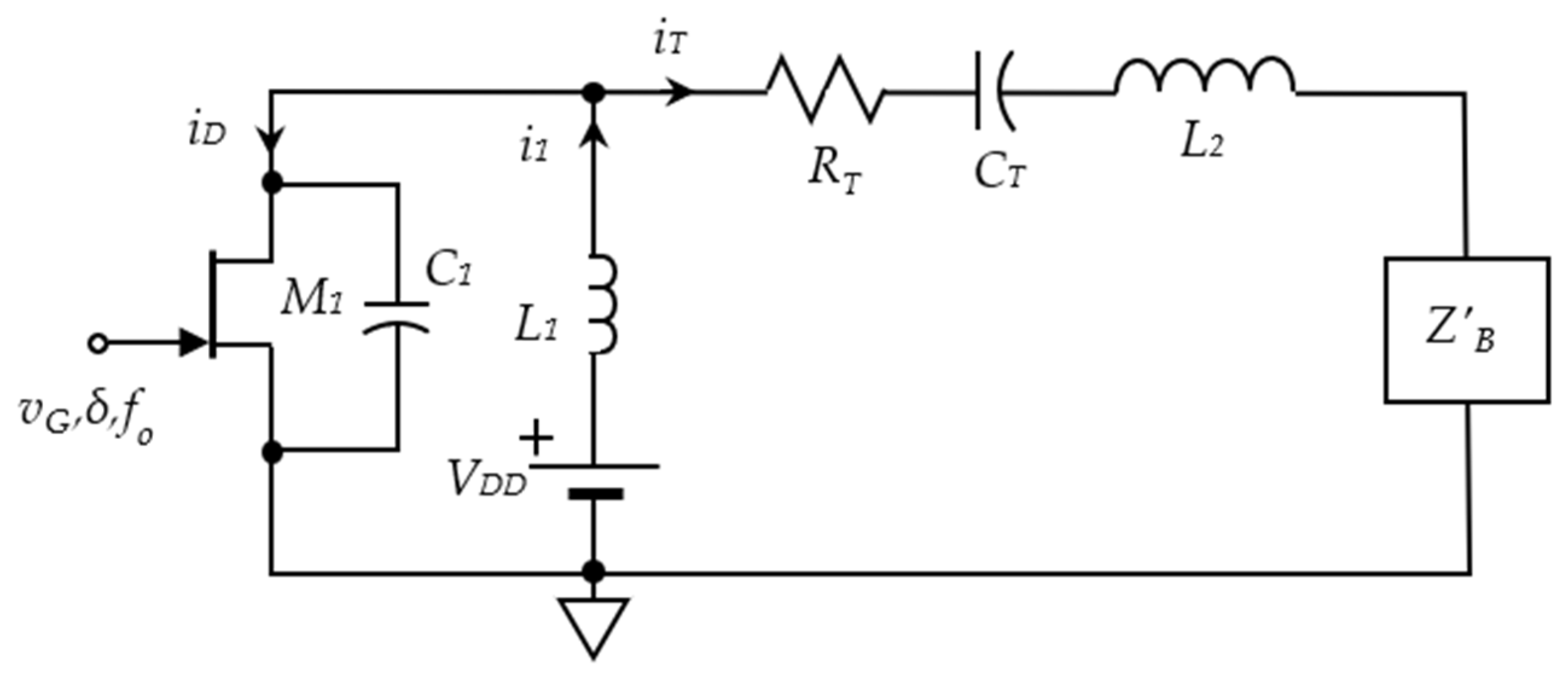
The resulting equivalent circuit for the resonant WPT is equivalent to the class-E circuit [12], as shown in Figure 1.
The increased current i 1 converts the electrical energy from the DC source VDD to the energy in the magnetic field using the electrical current, as follows.
d i 1 dt = V DD v x ( t ) L 1
The magnetic energy is then transferred to the impedance load side when switch M1 turns off. Therefore, the power delivered to load (PDL) is proportional to the amount of the magnetic energy absorbed into the inductor, which is a function of the current i1 increment. For achieving a higher PDL, we need to obtain the lowest v x ( t ) possible at the instant M1 turns on and M1 turns off when v x ( t ) rises back to VDD. The resistance RT denoting the coil resistance is preferred to be as small as possible to increase the power efficiency during WPT.
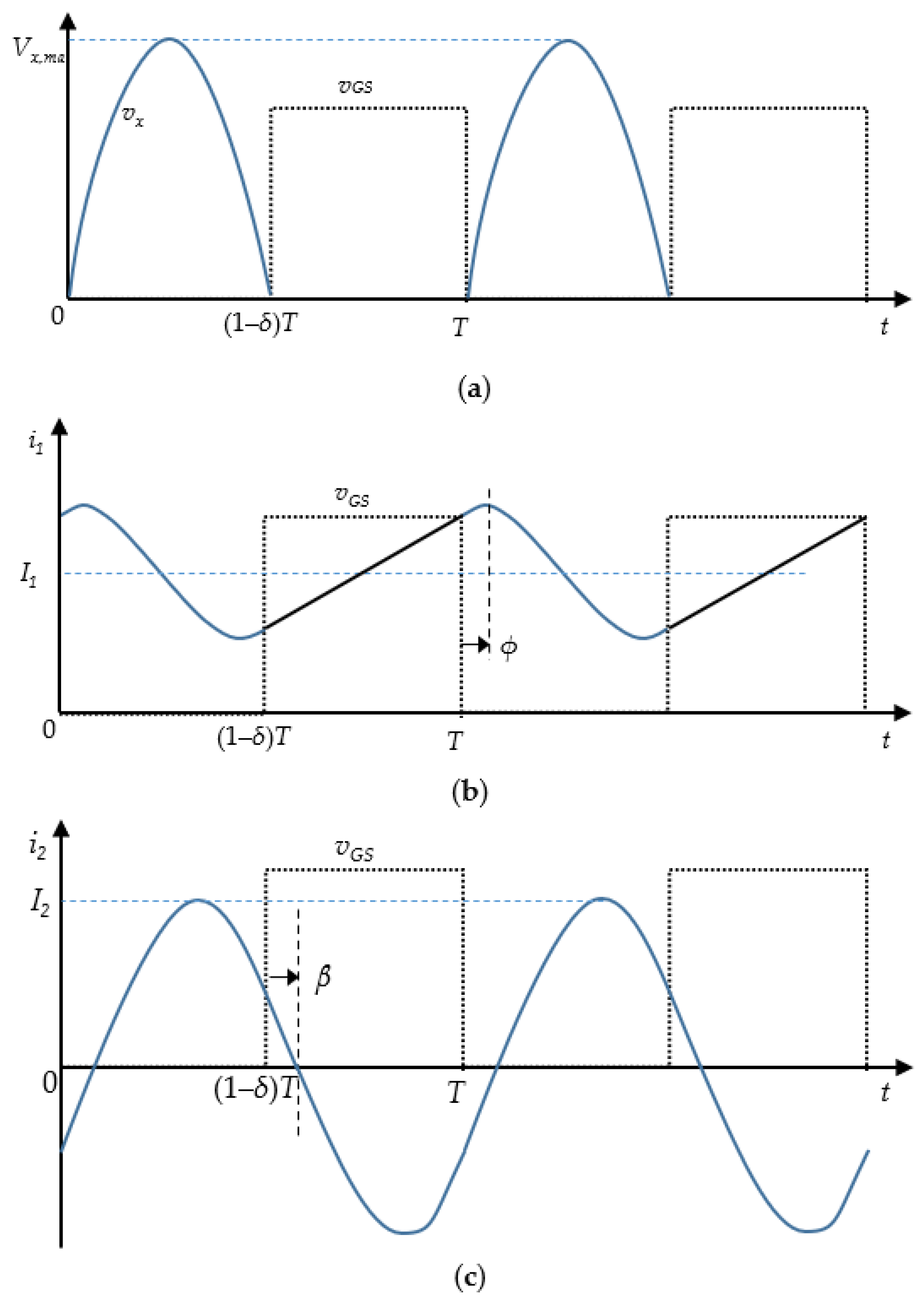
It was found [6] that the maximum value of the nodal voltage is a function of the current phase angle ϕ, as shown in Figure 2a, as follows.
V x , max = V DD 1 + 1 cos ϕ
where
tan ϕ π ϕ = δ 1 δ
The above equation is only valid for the zero-voltage switching control of the switch M 1 in the steady-state response, which may not hold for the transition states. The corresponding current phase angle ϕ is 64 0 and the corresponding voltage magnification V x , max / V DD is 3.28 at a steady state [6].
Parameters β and ϕ, derived in our previous work [24], are the key parameters for achieving the zero-voltage switching and zero-voltage derivative switching in the class E power amplifier (PA). Parameter ϕ, as shown in Figure 2b, denotes the phase difference between the phase of the device turning on and the phase that the maximum current flowing through L1 occurs, which is directly affected by the duty δ. Parameter β represents the phase difference between the device turning on and the current of the transmitter coil, as shown in Figure 2c. Both parameters β and ϕ are controlled by adjusting the frequency f and the duty δ so that the switching in the class E PA reaches the lowest power loss. The minimum power input control [24] is applied to avoid the situation in which the power transfer efficiency (PTE) goes down due to load variation, which determines the duty δ by trading off the power delivered to the load (PDL) with the PTE.

2.2. Power Receiving Unit (PRU)

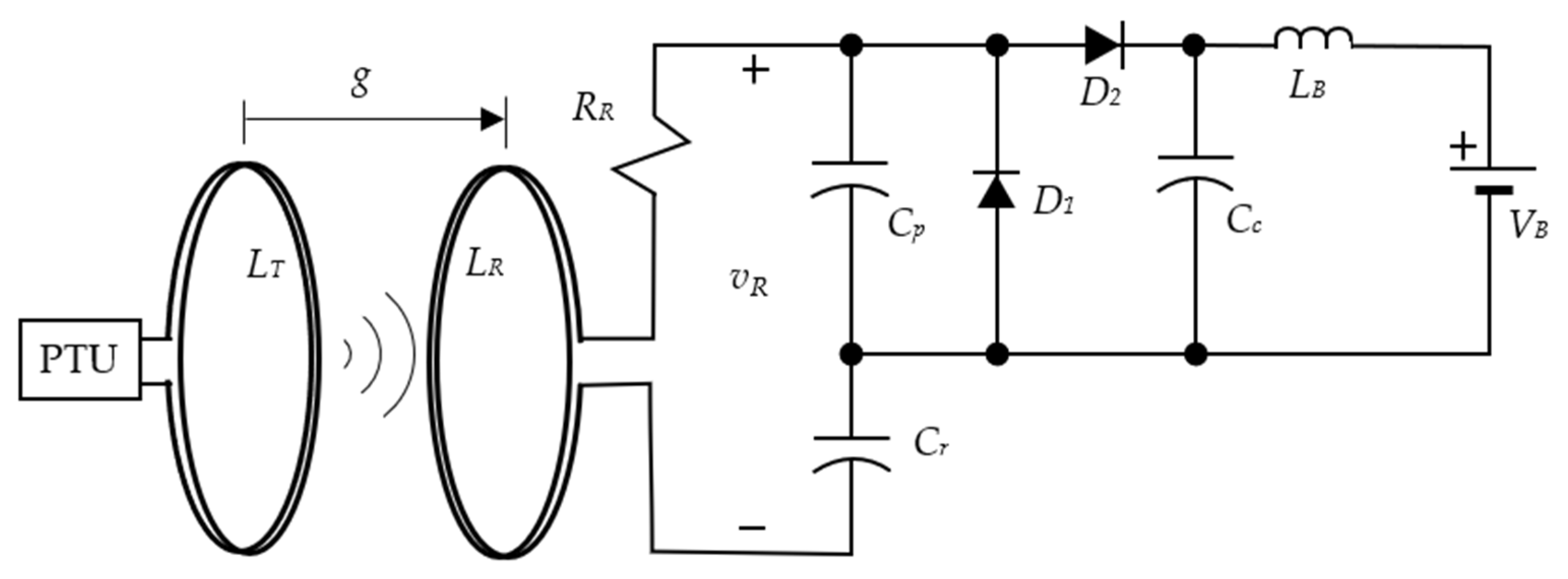
A specific kind of PRU is proposed in this paper, as shown in Figure 3. The impedance load is connected via the magnetic linkage between the PTU and the PRU. The receiving voltage swing on the PRU side is a function of the distance from the PTU coil and the condition of resonance determined by the PRU capacitance.
v R = v R ( f 0 , g , C r )
The receiving voltage amplitude on the PRU coil is a function of distance g away from the PTU coil and the condition of the resonance to the signal switching frequency f0. Among these parameters, the wireless signal switching frequency f0 is determined by the PTU which has to provide service to multiple users. The distance g of the specific PRU away from the PTU is a degree of freedom for the user. The PRU is allowed only to adjust the capacitance C r to achieve the best power transfer condition referred to as the minimum power input control.

2.3. Transformer Model for WPT

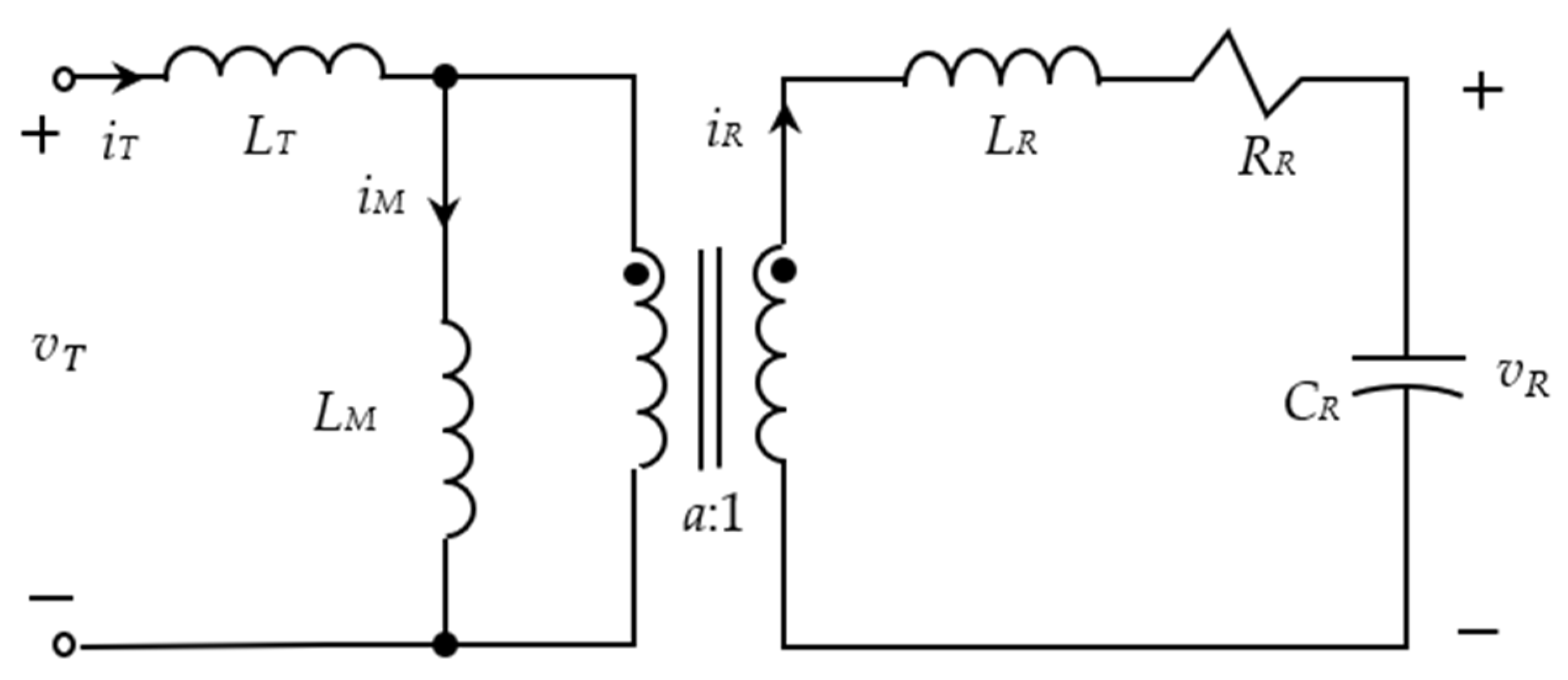
As WPT does not have a magnetic core, the equivalent circuit of the wireless transformer can be obtained by removing the core-loss resistance, which is in parallel with the magnetization inductance LM from the general version of the transformer, the Steinmetz equivalent circuit, and is shown in Figure 4.
The parallel quality factor Q P is derived in our previous work [12], as follows.
Q P = R R C R L R
where C R is the capacitance of PRU. The subscription capital R stands for receiving and is different from the lower r in C r , which stands for resonance.
When PTU and PRU have similar windings, i.e., LT = LR, the magnitude voltage gain G v , 1 is derived under the perfect resonance matching condition, i.e., the switching frequency 2 π f 0 = 1 / L R C R , as follows.
G v , 1 = v R v T = k k 2 + j Q P
The above equation ignores both the effects of the magnetization current flowing through LM and the coil loss through the coil resistance RT. k denotes the coupling coefficient between the transmitting and receiving winding coils. The coupling coefficient k is larger than Q P when the distance between the coils is small and is much smaller than Q P in the long distance WPT. The magnitude and phase of the voltage gain are expressed individually, as follows.
G v , 1 = k k 4 + Q P 2 G v , 1 = tan 1 Q P k = 0 ° pure   inductive   WPT 9 0 ° pure   Resonant   WPT
The resonance WPT transformer circuit model shown in Figure 4 acts as an impedance inverter that inverts the capacitor C R feedback to the class E PA. The equivalent feedback impedance Z FB mapped from the PRU to the PTU is derived as follows.
Z FB = 1 G v , 1 2 1 j ω 0 C R
where
ω 0 = 2 π f 0
The above equation is analogous to the transformer of the turn ratio 1 : G v , 1 . Because the turn ratio is a complex number, the capacitor is a negative capacitor, which is equivalent to an inductor with the inductance derived as follows.
L 2 = Q p 2 k 2 1 ω 0 2 C R = R R 2 k 2 C R
We let the undamped natural frequency of PTU be denoted by ω 2 , as follows.
ω 2 = 1 L 2 C T = k R R 1 C R C T

2.4. GaN HEMT Module

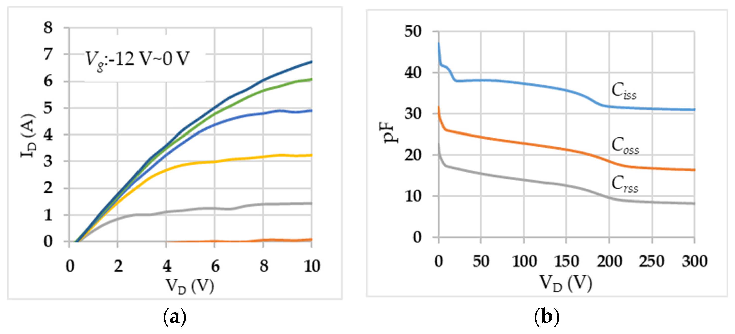
The study employed a D-mode GaN HEMT. The D-mode GaN HEMT manufactured in the Compound Semiconductor Laboratory (CSDL) of the National Yang-Ming Chiao-Tung University has been reported in the literature [6,12,24,25]. The newly developed 20 mm device with its ID-VD curve (shown in Figure 5a) indicates that the on-resistance was 0.9 Ω under a drain-source voltage of 2 V. The C-VD curve shown in Figure 5b was taken from the B1505A semiconductor analyzer, and shows an extremely low input capacitance (Ciss), which allows the switching frequency to be higher than 50 MHz. In our study, we connected three 20 mm devices in parallel to yield a larger current subjected to the side effect that the input capacitance was tripled and the switching frequency was lowered down to less than 16 MHz. This device boasted a total gate width of 20 mm, offering a current density of 500 mA/mm and an on-resistance of 50 mΩ/mm. Notably, it possessed a breakdown voltage of 600 V and a gate threshold voltage of −9 V. The accompanying parasitic capacitances and other pertinent characteristics are comprehensively outlined in Table 1.
To address packaging concerns, the 20 mm D-Mode GaN HEMT was encased in a Transistor Outline 220 (TO220). While the Dual Flat No-Lead (DFN) package, which could effectively minimize the impact of the stray inductance, the TO220 packaging exhibited a better thermal resistance. The reduction in the width of the GaN HEMT device represented a significant improvement over our previous version, which had a total gate width of 120 mm and was encapsulated in a TO220 package. The 20 mm D-mode GaN HEMT presented a six times smaller parasitic capacitance compared with the 120 mm version. The utilization of the 20 mm D-mode GaN was particularly advantageous for high-frequency operations within the MHz range, rendering it an optimal choice for resonant WPT.

2.5. Subharmonic Oscillation

Subharmonic oscillations, whose frequency was a fraction 1/n (n = 2, 3, 4,…) of that of the applied force term, can frequently occur in nonlinear systems [23]. These were found in both the theoretical results and experiments conducted for an electrical oscillatory circuit containing a saturable iron-core inductance and capacitance. The PRU proposed in this paper used the diodes with a nonlinear current output with respect to the input voltage across the diodes. The diodes turned on and off in accordance with not only the voltage, but also the current itself in a practical model of the high frequency, high voltage SiC diode. The nonlinear differential equation could produce subharmonic responses with a frequency that was a fraction of the input—the fixed frequency. The individual terms in the nonlinear differential equation needed to include the instantaneous states of voltage and current. In our experiments, the subharmonic response occurred when the DC supply voltage V D D on the PTU side was higher than the voltage level that occurred when the voltage- gain between the PRU coil and PTU coil was higher than the conducting threshold voltage of the diodes in PRU. In this paper, we only showed the existence of subharmonic responses instead of providing complete theoretical results as the comparison.

3. PRU Module for Battery Charging

3.1. AC-DC Converter

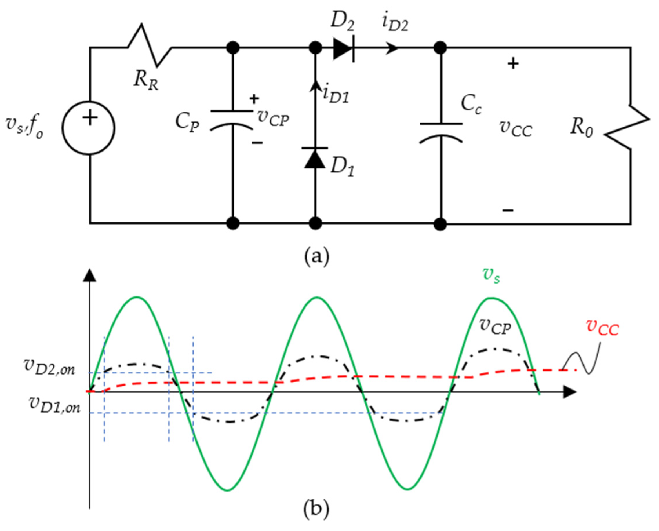
An AC-DC converter circuit using a diode rectifier is shown in Figure 6, which has the advantage of converting the high voltage AC source into a low-voltage DC storage. Diode D 1 is used to prevent negative charging into the capacitor C P . Diode D 2 works together with capacitor C c , which is the peak detector circuit. The two diodes turned on alternatively to limit the voltage in capacitor C P ; thus the capacitor voltage on C P is derived for the low current as follows.
V D 1 , on v CP v D 2 , on + V Cc , min
The charging time of capacitor C P must be smaller than the period time of the input source V s ; however, the smaller the resistance of R R , the larger the resistive loss of the converter when the voltage turns into a negative cycle. In practice, the high frequency diode resistance is 0.2 Ω, thus the capacitor voltage v CP can be increased by the actual voltage across the diodes, as follows.
V D 1 , on + I D 1 , max R D 1 , on v CP V D 2 , on + I D 2 , max R D 2 , on + V Cc , min
The peak detector capacitor voltage v CC is a function of charging through resistor R R up to V s v D 2 , on and discharging from the load R 0 . Assuming R R is very small, we can then find the steady state result of the minimum value of the capacitor voltage C C c , m i n as follows.
V Cc , min = V s V D 2 , on 1 e 1 / ( 2 f 0 R R C c ) e 1 / ( 2 f 0 R 0 C c ) e 1 / ( 2 f 0 R R C c ) V s v D 2 , on e 1 2 f 0 R 0 C c
The maximum current of diodes D 1 and D 2 can be obtained as follows.
I D 1 , max = V s V D 1 , on R R I D 2 , max = V s V D 2 , on V Cc , min R R
When subjected to a heavy load R 0 , the two diodes have the same maximum current, i.e., I D 1 , max I D 2 , max .

3.2. Resonant Capacitive Voltage Divider

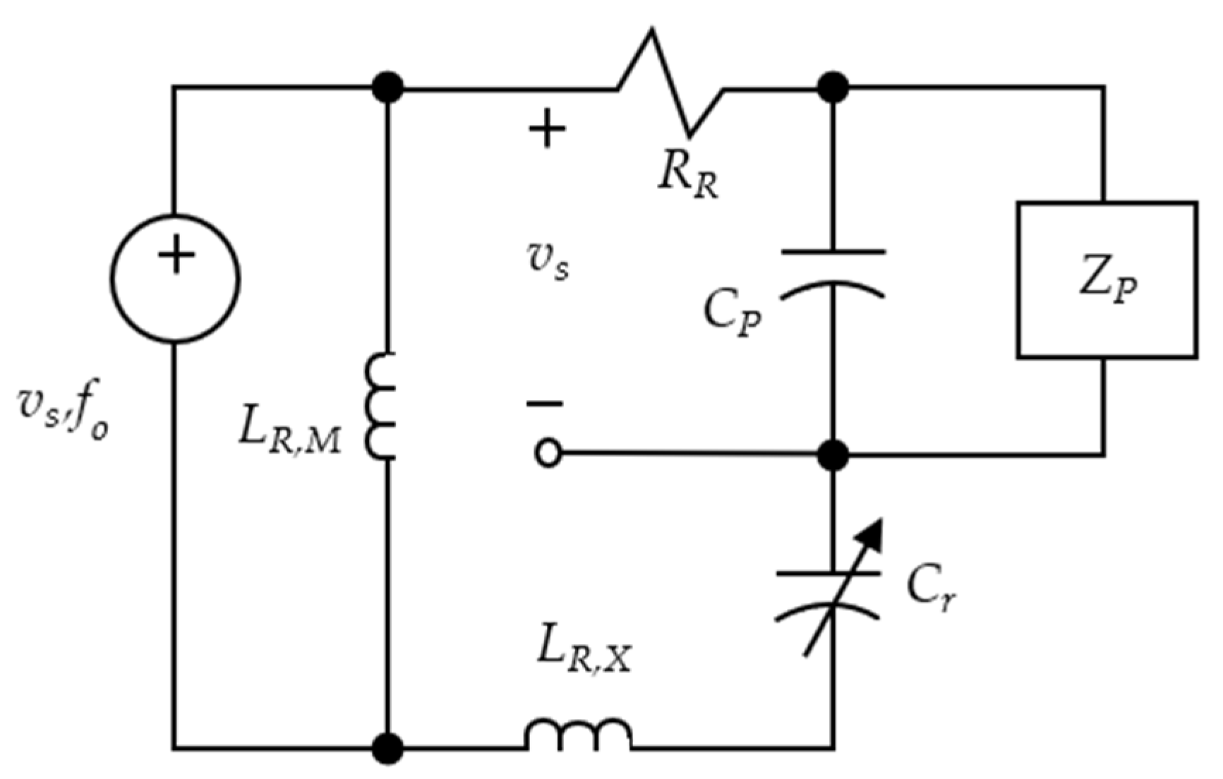
The input source to the AC-DC converter is a resonant capacitive voltage divider that is modeled as shown in Figure 7. The capacitor C R is adjustable to tune the series resonance between itself and the processing capacitor C P with the inductor L R . It is assumed that a very small part of the inductor L R acts as the magnetization inductor L R , M as a secondary coil of the transformer and the rest of the inductance L R , X into the leakage inductor. The resonant voltage is typically higher than hundreds of volts. For achieving the voltage reduction and maintaining the resonance phenomenon, capacitor C P inserted in series with the resonance capacitor C r in the LC tank integrates a new total capacitance.
C R = C r C P C r + C P
The voltage resonance occurs when the resonant frequency of the series LC tank f LC matches the input frequency f 0 , provided the leakage inductance is much larger than the magnetization inductance, i.e., L R L R , X , as follows.
v s = C r C r + C P v R
The voltage resonance occurs when the resonant frequency of the series LC tank f L C matches the input frequency f 0 , provided the leakage inductance is much larger than the magnetization inductance, i.e., L R L R , X , as follows.
f 0 = f LC = 1 2 π L R , R C R 1 2 π L R C R
Adjusting the capacitance of C r which subsequently changes C R , we can tune the resonant frequency of the series LC tank with the equation as follows.
f LC = 1 4 π L R C R 3 2 L R C R C r C r = C R 2 f LC C r 2 C r
As the exact f LC is unknown when completing the adjustment but the transmitting frequency f 0 is known, the following equation can be used in tuning, provided that C P >> C r .
f LC f 0 = K f C r C r
where
K f = C P 2 C r
The above equation is stated as the percentage change in capacitance, which is proportional to the ratio of C R and C r . To allow for a low sensitivity of capacitance adjustment, which is preferable to the fine tune, the capacitance of C P is reduced. But, on the other hand, the voltage across the load is also increased to a very high voltage, which is unfavorable to the heavy load Z P application, which can take too much charge from the resonance LC tank and break the resonance mechanism.

3.3. Battery Charger Using a Flat-Band Band-Pass Filter

The output load of the AC-DC converter is a resonant capacitive voltage divider, which is modeled as shown in Figure 8a. The battery can be modeled using a resistor R B , representing the electrodes and interlayer connection loss; a capacitor C B , representing the instantaneous capacitive behavior for charge storage; and an ideal DC voltage source V B . The resistor R B is temperature-dependent, which is typically around 0.1 Ω at room temperature for the Lithium-ion battery. The capacitor C B is typically thousands of Faradays for each individual Lithium-ion battery. The input source of the battery charger is a DC voltage source v cc superimposed with an AC voltage source v cc . For reducing the energy loss of the low-pass filter, aside from a low-resistance resistor R B , we used an inductor to serve as a choke to absorb the voltage difference between the input voltage and the battery DC voltage V B . The governing equation for the current to charge the battery capacitor C B of the circuit in Figure 8a is formulated as follows.
L B d i B dt + R B i B + i B dt = v cc + ( V Cc V B )
Providing the assumption of steady state when V B = V Cc , we derived the Laplace transformation between the AC voltage v cc and the output current i B as follows.
I B ( s ) V CC ( s ) = s L B s 2 + R B s + 1 C B
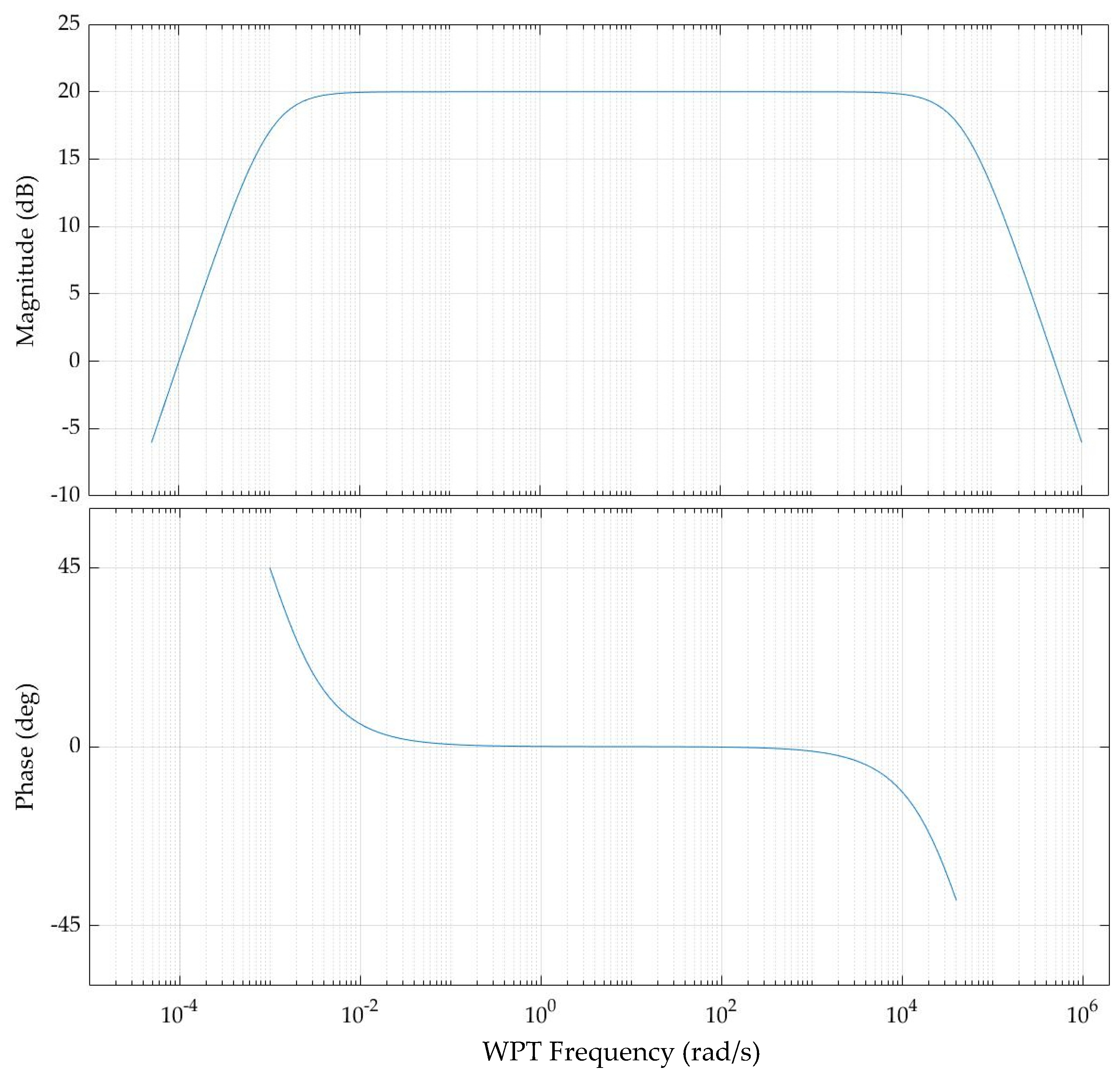
For the specific frequency f o of WPT in the range between 4 to 15 MHz, one may choose L B in uH, which, together with the large capacitance of C B and the zero at the origin, form a flat-band band-pass filter that has a low voltage gain on the high frequency component and that also has a low voltage gain on the ultra-low frequency component, i.e., the difference in voltage between V B and V Cc , to prevent the current surge from the battery during the initial charging. The alternative circuit to expedite the current surge from the battery during the connection of the battery to the circuit is to add a stabilization capacitor C a along with a diode, as shown in Figure 8b. We can use a diode to protect the reverse current flow from the battery to the inductor L B or even the high frequency stabilization capacitor C a on the AC-DC converter. Figure 9 demonstrates the Bode plot for the band-pass filter with L B = 2   uH , C B = 10,000   F , and R B = 0.1 Ω.
The equivalent impedance of the battery charger when assuming that the AC-DC conversion is at its steady state is derived as follows.
Z B = V s I B
Using the same parameters of L B = 2   uH , C B = 10,000   F , and R B = 0.1 Ω, we calculated the equivalent loading at a resistance 0.1 Ω with zero phase in a frequency band between MHz to 10 kHz.
Equation (21) shows a negative resistance, which can cancel out the resistance R T from PTU and even induce instability of WPT. At a steady state of resonance, the PRU circuit was an NIC that converted the positive resistance into a negative resistance within the bandwidth between sub-Hz to 30 kHz. For the resonant frequency component of the input signal, the PRU circuit converted the instantaneous capacitance of the battery into the inductance L2, as indicated in Figure 10. When the absolute value of the negative resistance of the impedance Z B was much higher than that of the PTU coil resistance, the LC tank in the PRU was associated with a negative damping, which could cause instability of the circuit response. Therefore, we will need closed-loop current control to stabilize the circuit in the future.

3.4. Magnetic Coupling Coefficient

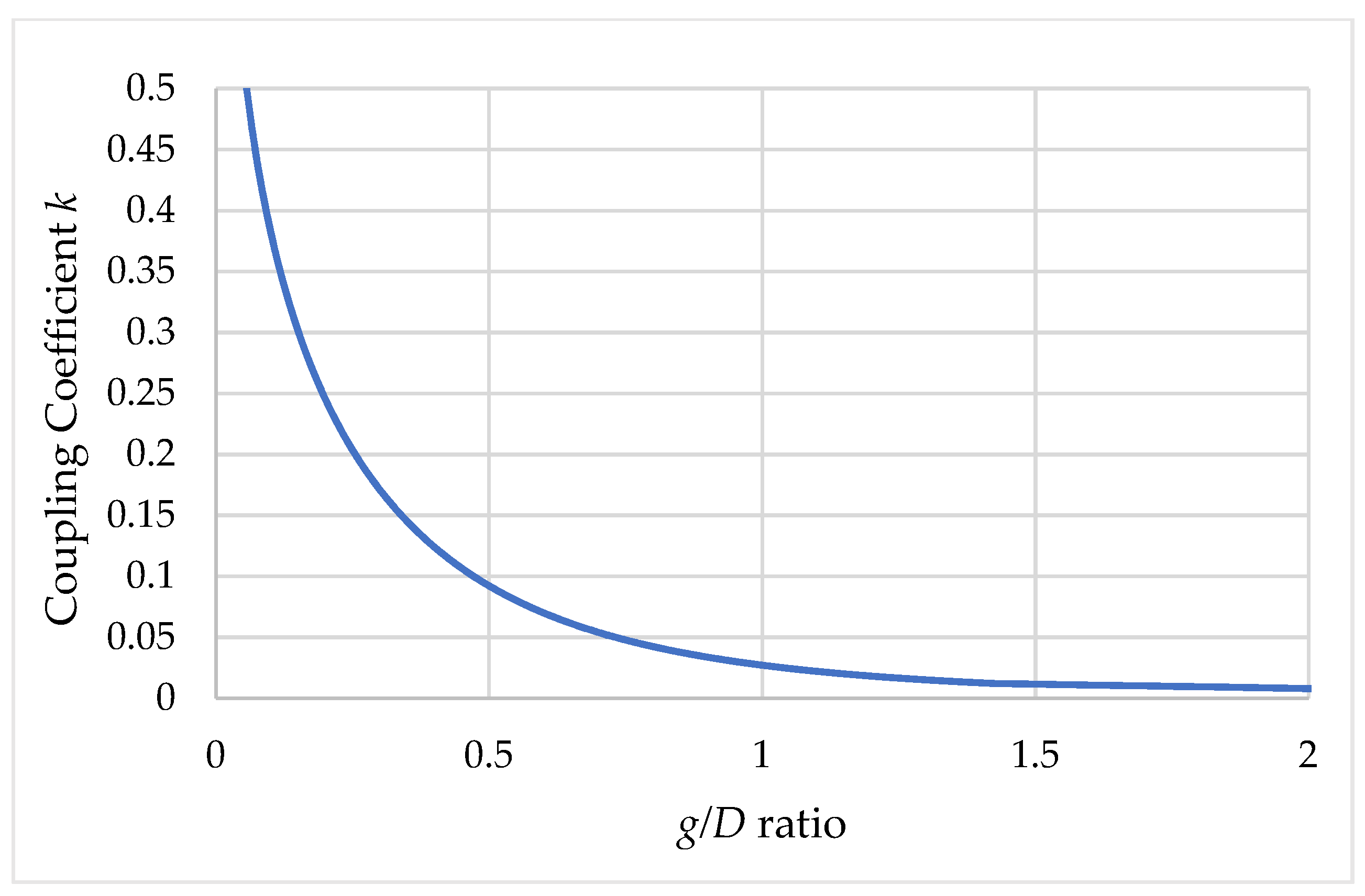
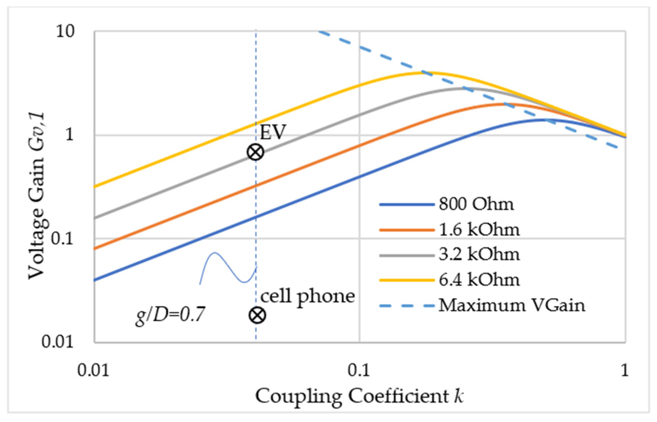
The coupling coefficient k is a function of the distance gap g between the transmitting coil and the receiving coils used in WPT. The factor of distance gap can be converted into the g/D ratio to simplify the actual effect to the coupling coefficient [12], where D denotes the coil diameter. The example that demonstrates the coupling coefficient decay with respect to different g/D ratios subjected to D = 70 cm is shown in Figure 11. It can be seen the coupling coefficient k was 0.1 when the PRU coil was 35 cm away from the PTU coil and the coupling coefficient k dropped to half of 0.1 when the PRU coil was 50 cm away. It was also proposed in [9] that the maximum voltage gain G v , 1 and the maximum power transfer could be obtained when the coupling coefficient k matched the parallel resonance quality factor Q P . It was then concluded that for the ultimately remote distance, we had to use the zero resistance coils, which could be easy to fulfill in outer space, but not on Earth. The loading placed in parallel with the LC tank could also affect the parallel resonance quality factor Q P , which caused degradation of the voltage gain, as shown in Figure 12. The battery voltage V B attached to the proposed PRU was a kind of loading that could be equivalent to the resistive loading when the charging current was flowing through the battery. For a heavy load, i.e., smaller equivalent resistance, the voltage gain was smaller and thus a smaller equivalent resistance among the power transfer could be achieved when the battery was charged with a large current. As for the same battery voltage V B , the equivalent resistance became smaller when subjected to a larger current. This also implies that it was preferable to charge a longer battery string with a higher voltage in order to reduce the equivalent resistance. EV applications, where the battery voltage can be as high as 300 V, could be an ideal application for the resonant WPT to transfer high power.
Different applications, including cell phone charging with a voltage V B = 5   V under a charging current of 1 A and EV charging with V B = 132   V under the same charging current of 1 A, were used for comparison. Using C r = 200 pF and C P = 5 nF , the voltage division was 25 times, according to Equation (15). For the case of cell phone battery charging, the equivalent resistance was 5 Ω × 25 = 125 Ω, and the voltage gain could be as small as 0.02 when g/D = 0.7. For the case of EV battery charging, the equivalent resistance was 132 Ω × 25 = 3.3 kΩ, and the voltage gain could be as small as 0.8 for the same distance g/D = 0.7. There had to be a higher V D D input than that of the EV application in order to charge the cell phone due to their equivalent loading differences, as shown in Figure 12.

4. Simulation and Experiment

4.1. Simulation

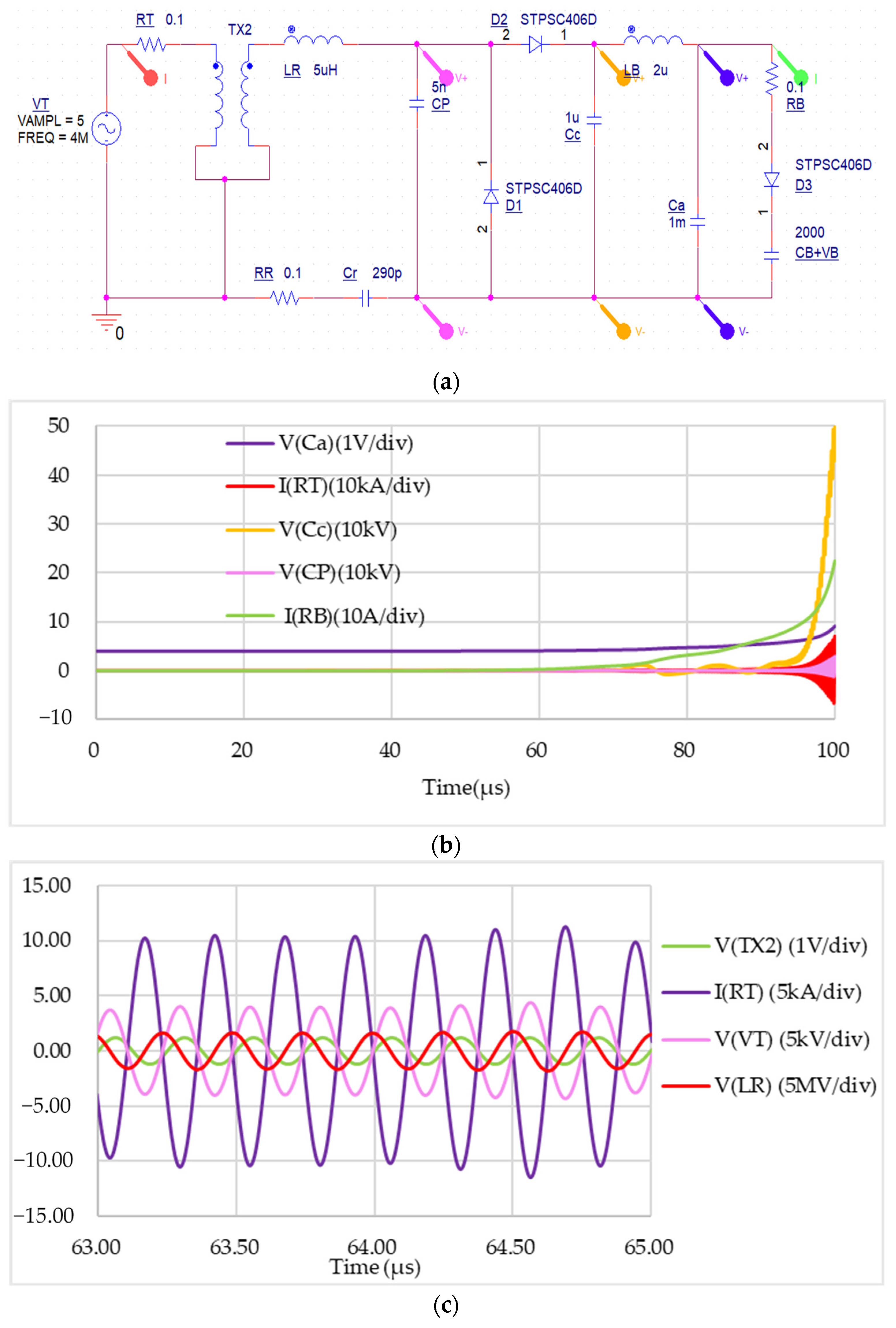
We adopted two simulations: one was used to identify the effect of PRU alone and the other was used to identify the PRU function inside of the resonant WPT with a class E amplifier. The first simulation configuration is shown in Figure 13a, which applied the circuit parameters as shown in Table 2. Both the battery capacitor and the stabilization capacitor C a were initialized with a voltage of 4 V. The instability current, as observed in Figure 13b, shows that the charging current towards the capacitor ramped up quickly after 100 μs of simulation time. The circuit became unstable, which turned to Mega-watt charging in the battery in 300 μs of simulation time. This was due to the PRU AC-DC output capacitance C c (scale 10:1; in gold color line) being charged with a high enough voltage to feed into the PRU stabilization capacitance C a (in blue color line). The battery charging current (in green line) dramatically increased when the voltage in C a was above the battery voltage and the diode threshold voltage, which simultaneously increased the input current (scale 1000:1; red line). Both the PRU resonant capacitor and the AC voltage divider capacitance voltages increased due to the current resonance. Taking a closed examination of the phase change of the voltage and current with different color markers on the same circuit, as shown in Figure 13c, we zoomed into the time duration between 63 μs to 65 μs before the power burst occurred. We compared the time (phase) basis with an input of 5 VAC (in purple line), and found that the voltage v T (scale 1000:1; in green line) on the primary winding varied from a 2 0 0 phase lead at 63 μs to a nearly 12 0 0 phase lead at 65 μs. The voltage v R (scale 1 0 6 :1; in red line) on the primary winding varied from a 22 0 0 phase lag at 63 μs to a nearly 9 0 0 phase lag at 65 μs. This was also when the voltage v R and the voltage v T reached a 9 0 0 phase, yielding a resonance condition satisfying Equations (5) and (6) with a voltage gain G v , 1 of nearly 1000.
This simulation was an unrealistic WPT, as the voltages could not be as high as 1 mega-volt in real applications, when most capacitors endure 1000 volts and the voltage gain G v , 1 could not be 1000 for long-distance power transfer with a low coupling coefficient k. However, it is still very valuable to understand the resonance mechanism as well as the proper function of the PRU circuit from this simulation example. It can be observed from Figure 13b that the voltage in capacitor C c was oscillating at a subharmonic frequency of around 10 kHz. The current ramp was, in a sense, an exponential growth form, which is known as instability. The battery voltage V B was 4 V in the simulation because it took a very long simulation time to reach the instability of the current when a larger battery voltage was applied. In the experiments, we used a high battery voltage to attain a similar instability current effect.
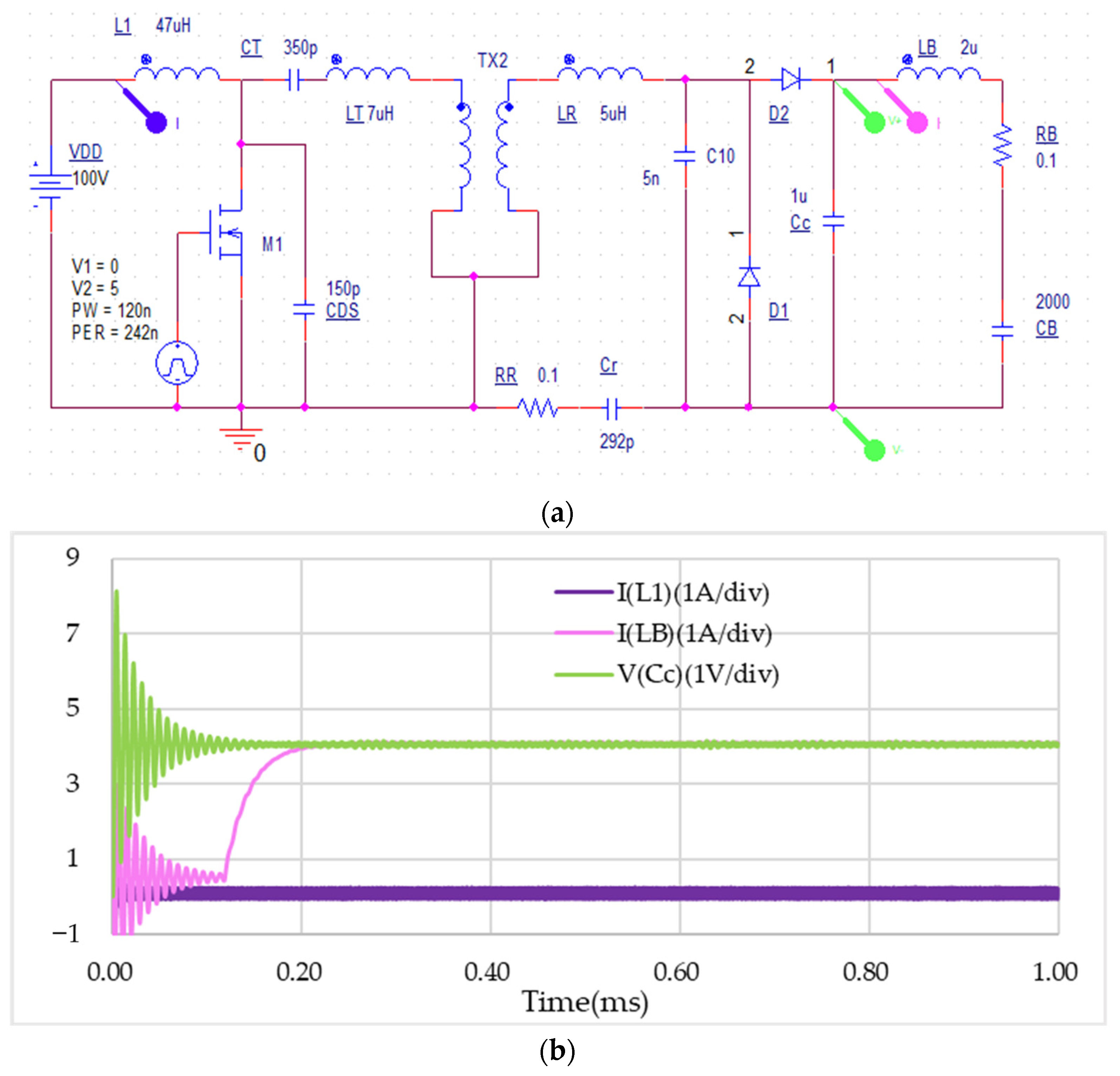
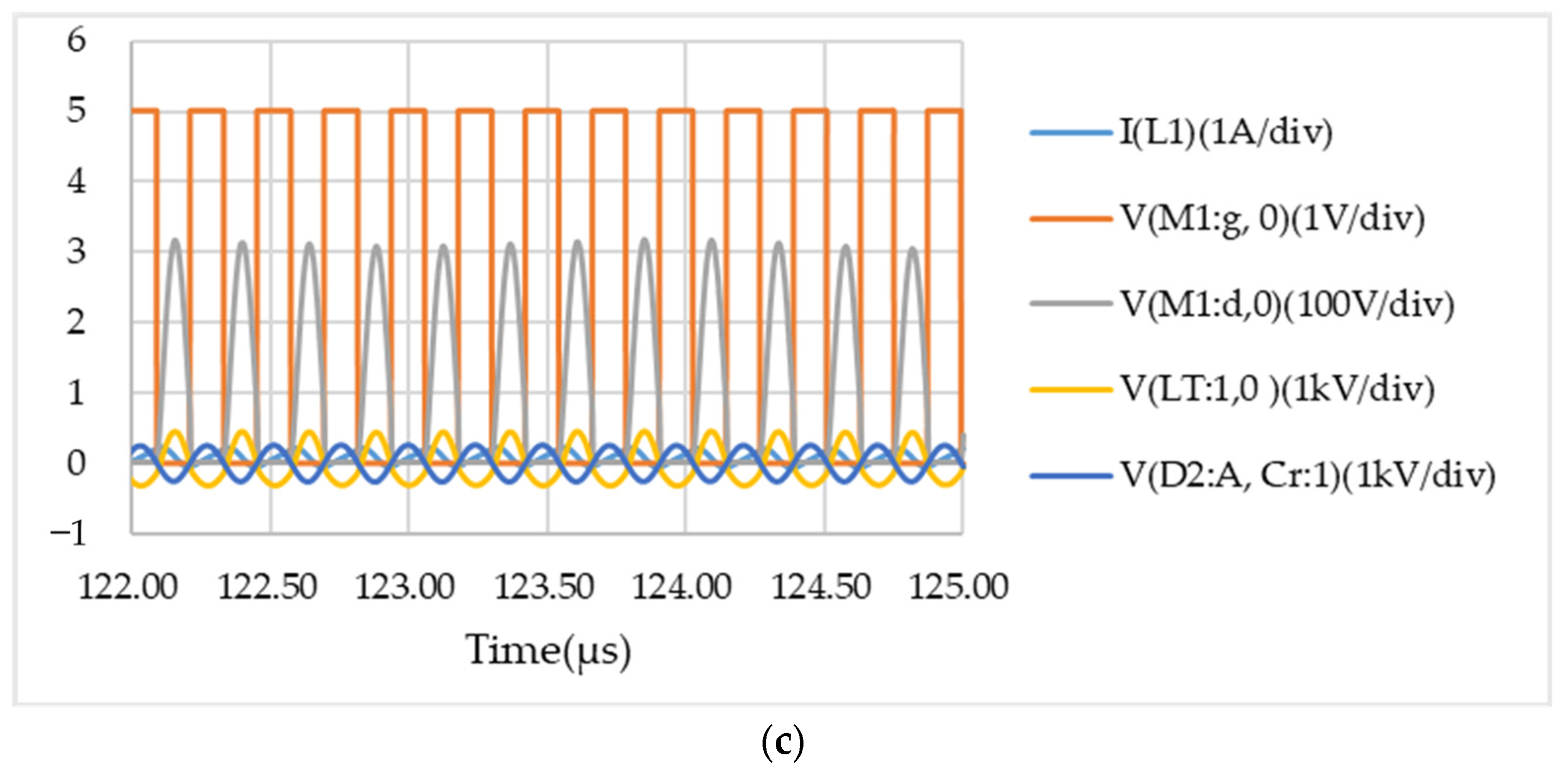
The second simulation was based on the class E amplifier instead of an AC voltage source, which could easily deliver a high power with a high voltage at a high frequency of around 4 MHz. The operating frequency of 4 MHz was obtained based on the current experimental layout. Using the minimum power input control [24] mentioned in Section 2.1, we found that a frequency of 4 MHz along with a duty δ for controlling both parameters β and ϕ yielded the lowest power loss. The class E amplifier was similar to the boost converter. except the output was a LC tank, as shown in Figure 14a. In the circuit, all parameters used for PRU were identical to the previous simulation example, except for the resonance capacitance C r which was micro adjusted to 392 pF for the resonance; in addition, the stabilization capacitance was omitted from the circuit. The resonance occurred immediately after the circuit was turned on in the simulation, which did not need a stabilization capacitance to assist. The reason the circuit could reach the resonance much faster than when using the AC voltage source could be due to the precise matching of the resonant frequency or because the class E amplifier was self-adjusting to the resonance. The corresponding results are shown in Figure 14b. The AC-DC output capacitor C c first oscillated for a while before reaching a higher voltage than the battery voltage, i.e., 4 V, and soon after, the charging current rose up and reached 4 A. The charging current still carried some high frequency ripples, as indicated in the wide-band filter result of Equation (20). The input current occurred after the increase in charging current. As the battery voltage was set to 4 V, the output power was calculated as 4 A × 4 V = 16 W. There was no negative resistance effect of PRU in the previous example because a steady state existed for the class E amplifier circuit. Taking a closer look at the time duration between 122 μs to 125 μs before the charging current ramped up, as shown in Figure 14c, we observed that ZVS gradually formed from the wave form of the transistor v DS (scale 100:1; in gold line) when compared with the v GS (in red line) turn-off time. It was also observed that the phase difference between the voltage v T (scale 1000: 1, in green line) of the primary winding and the voltage v R (scale 100: 1, in green line) of the secondary winding became 9 0 0 , which matched the resonance condition in Equation (6). The current I 1 on inductor L 1 increased during the transistor turn-on time, and the current phase angle ϕ was around 64 0 and the corresponding voltage magnification V x , max / V DD was also around 3.28, as expected in Equation (2) of Section 2.1 for the steady state. This shows that the class E amplifier could work just fine with the proposed PRU module. In this simulation, the switching frequency was 1000/242 = 4.1 MHz and the duty was 120/242 = 49.6%. The voltage gain G v , 1 observed from Figure 14c was 120 V/500 V = 0.24, which was achieved in the real resonant WPT application, with quite a large distance gap g in the measure of diameter of the PTU coil.
The control system will became unstable when the resonance with a very high voltage gain G v , 1 was achieved by adjusting the PRU resonance capacitance. Figure 15 shows the instability response when the resonance capacitance C r was micro adjusted to 292.1 pF. With a slight variation in the resonance capacitance C r , the LC tank changed from a stable circuit to an unstable circuit. An on-line monitoring of PRU is therefore needed in practical applications, and PTU could be controlled to avoid instability. Both simulations above used the same coupling coefficient k = 1 as the instability phenomenon would still occur with different coupling coefficients, and only the simulation time to reach instability would increase due to smaller values for the coupling coefficient k. When we examined the output wave form (red curve trace) of the charging current flowing into the battery, we observed the subharmonics f s / n of around 100 kHz and other lower frequencies.
The numerical study based on concurrent electronic design automation (EDA) tools such as the OrCAD 17.2-2016 PSpice software makes it difficult to accurately analyze the nonlinear networks. Open-source software, such as YalRF [26] or the commercial software Advanced Design System 2024 Update 1.0 (ADS) [27] from Keysight Technologies Inc. (Santa Rosa, CA, USA), can be used to find the steady-state response of autonomous circuits with periodic and quasiperiodic responses based on the Harmonic Balance method [28]. These software tools are not yet comprehensive for the circuit designer without knowing the parameter-dependent subharmonic frequencies. The PTE and PDL analyses for the current nonlinear network, provided in Figure 16, were performed in this research using a quasi-static analysis with the following seven steps.
(1)
Assigning the voltage of the battery V B ;
(2)
Performing OrCAD PSpice analysis with proper selection of the run-to-time, around 300 us in our study, and step-size, 1 ns in our study;
(3)
Exporting the trace data of the power dissipation elements such as diodes, resistors, and transistors;
(4)
Exporting the trace data of the battery to calculate the output power;
(5)
Selecting the maximum current, 100 A in this study, to define the valid trace data range;
(6)
Performing the calculation of the output power by multiplying the input current with the battery and the voltage of the battery itself;
(7)
Performing the calculation of the input power by adding the output power together with the power losses from all of the power dissipation elements.
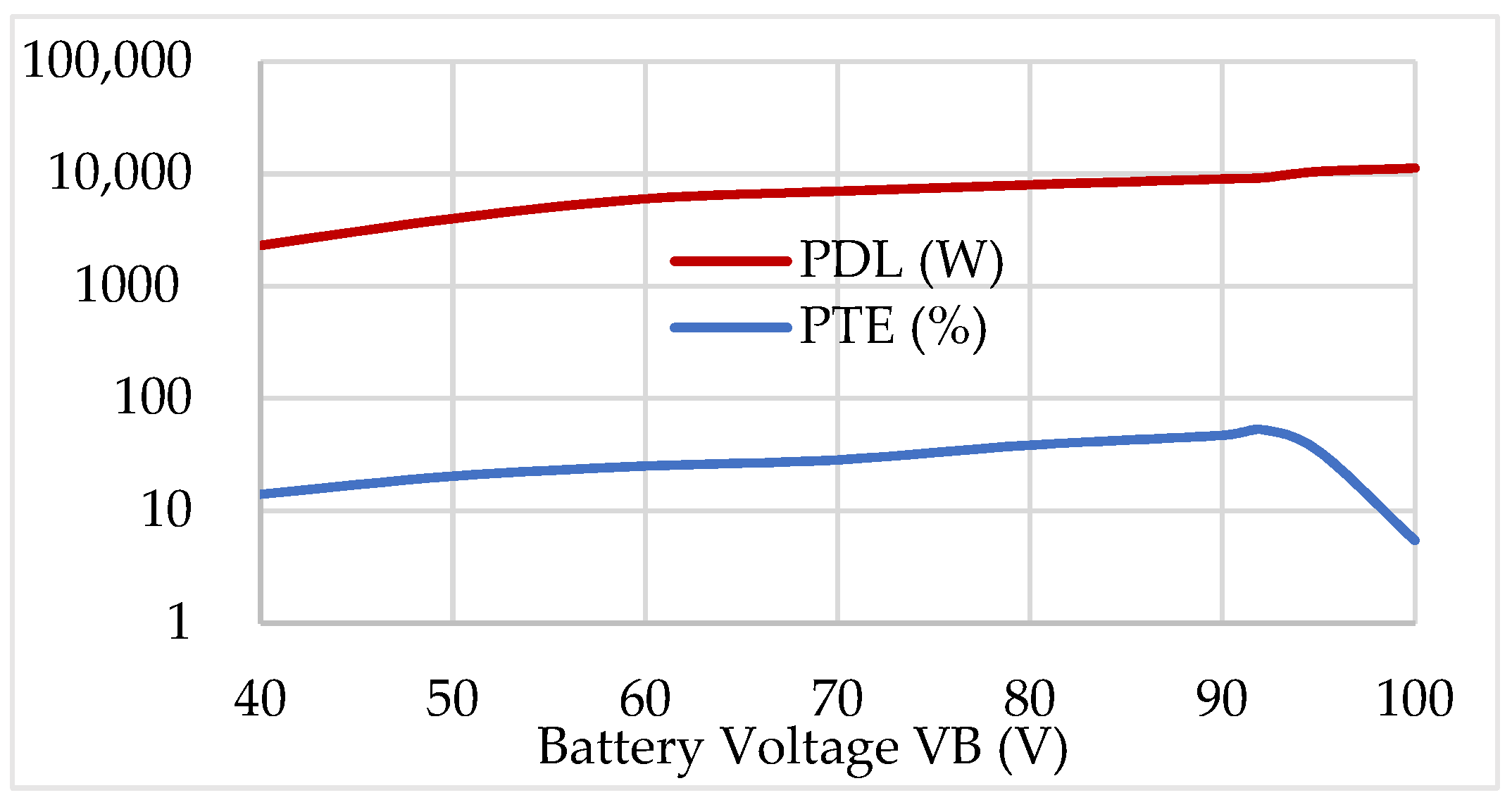
The reason the seven-step analysis was used instead of directly calculating the input power on the PTU side is that there was still conservative energy stored in the capacitors and inductors at the instant when the result diverged. Miscalculation of the conservation energy would cause the actual input power to be seriously underestimated. Following the seven-step analysis, we could obtain a quasi-static analysis result, as shown in Figure 16. The result showed that the maximum power transfer efficiency (PTE) was 53% under a battery voltage of 92 V. Above the 92 V battery voltage, the PTE dropped dramatically due to high current oscillation that presented in the beginning of the analysis. PDL monotonically increased with the battery voltage.

4.2. Experiment

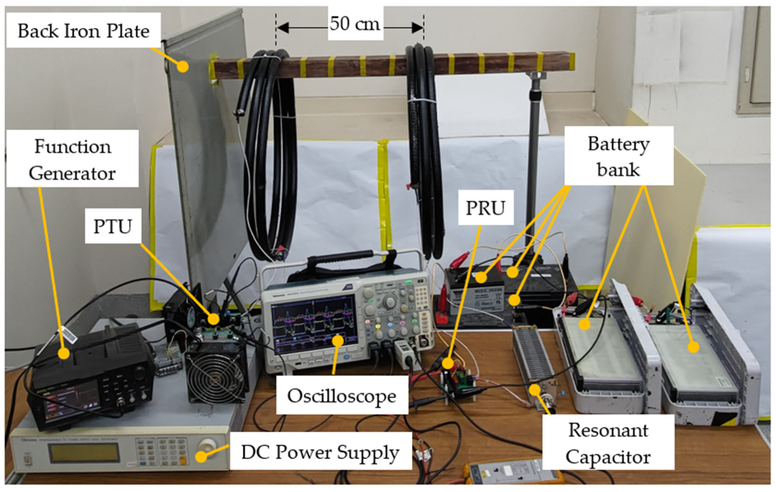
The experimental layout included a PTU consisting of a class E amplifier and a transmitter coil, a PRU consisting of the PRU circuit and a receiving coil, a DC power supply, and a function generator to control the PTU switch, as shown in Figure 17. The back-iron plate was isolated from all of the devices. The two coils were placed 50 cm away from each other, measured from the center of the coils. The 50 cm distance was predetermined from previous experience [12], according to Figure 12, in which the optimal distance was 70% of the coil diameter, which was 72 cm in this study. The PTU switch integrated three 20 mm GaN devices connected in parallel, which were all D-mode GaN HEMT driven by the charge pump gate drive. The resonant capacitor was in series of a ceramic capacitors with an adjustable capacitor that was used to tune the resonance capacitance to match with the switching frequency of the PTU switch. Each of the 20 mm GaN devices was able to conduct 6 A DC current. In the class E amplifier, the maximum current flowing on the switch was 2.5 times that of the DC current read from the power supply when the duty cycle of switching was 50%. Therefore, the maximum power that could be delivered from the PTU under VDD = 90 V input was 3 × 6/2.5 × 90 = 600 W. Considering the switching loss among the GaN HEMT switches, we had to confine the maximum output power from the DC power supply within 350 W by setting the maximum current output of the DC power supply into 3.5 A in the experiment. The battery string we used in the experiments consisted of two 48 V Lithium battery packs and three 12 V lead-acid batteries, which were all used for different EV applications. The batteries were connected in series, which together resulted in 132 V terminal voltage. The purpose of this experiment was to demonstrate that the EV battery could be charged with 1 A current using the resonant WPT techniques with PRU.
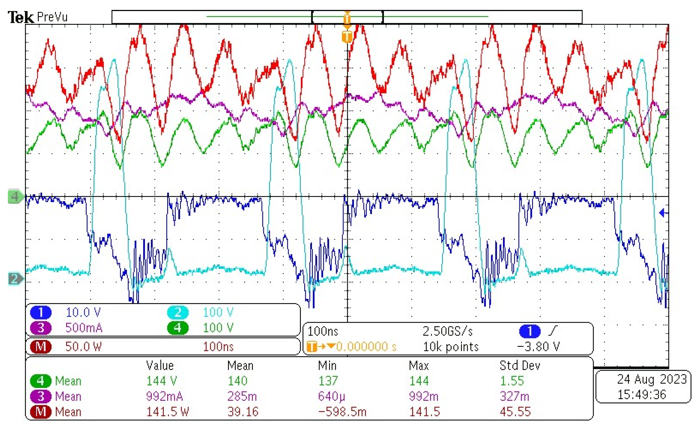
Figure 18 shows the oscilloscope screen dump at one instance during battery charging. The dark blue color trace shows the V G S of one of the D-mode GaN HEMT switch, which had a threshold voltage of −7 V for turning on the switch, which also indicated that the duty of switching was 0.5, i.e., 50% of the time V G S was below −7 V. The cyan color trace shows the V D S of one of the D-mode GaN HEMT switches, which had a maximum V D S of 500 V, which was actually as high as 700 V before the current limit was reached. The green trace shows the battery voltage V B , which oscillated between 200 V to 80 V during battery charging. The purple trace shows the battery current I B flowing through the battery string, which showed an average charging current of 992 mA and no discharging current flowing through the battery, even when the battery voltage was below 132 V. From the positive charging current point of view, it can be concluded that the battery voltage oscillation could be due to the measurement of the connection wire between the batteries via the high frequency magnetic flux. The red color trace shows the calculation conducted by the oscilloscope internally, which showed an average of 141.5 W going into the battery charging. At the same time, we compared the parameters of our experiment with the results from the simulation, as shown in Figure 19.
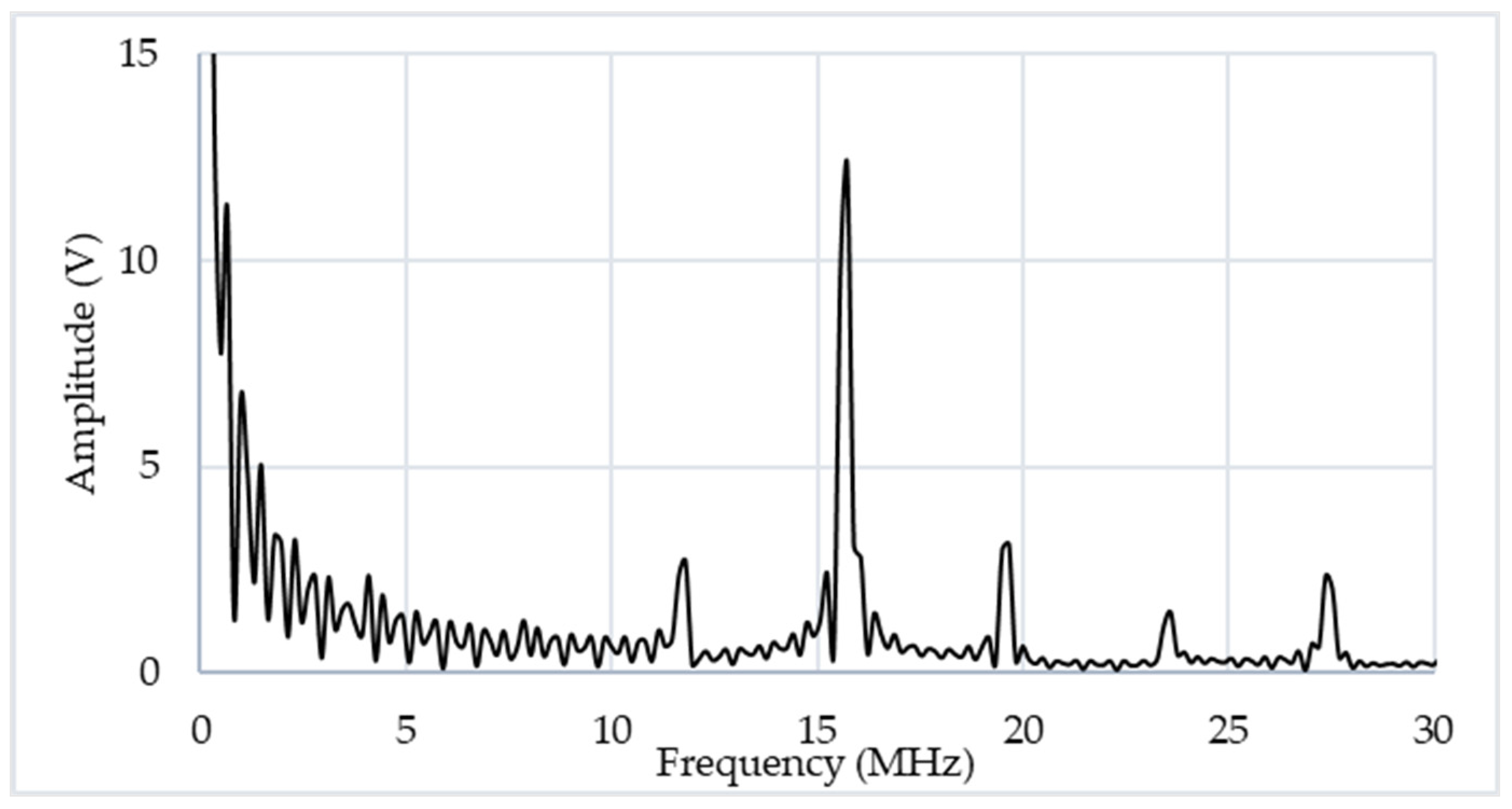
The battery voltage varied during battery charging due to its SOC (state-of-charge)-VOC (voltage-of-open-circuit) characteristics [29]. The subharmonic oscillation that resulted from both the PRU nonlinear network and the battery characteristics could be analyzed using the harmonic balance method. Thus, we converted the experimental data of the battery voltage into the frequency spectrum in order to understand the subharmonic frequencies. As shown in Figure 20, the major subharmonic frequencies occurred at 15.72 MHz, subjected to a switching frequency at 3.65 MHz. As most of other subharmonics were nearly equally spaced, they were more like the harmonic spurs and were therefore ignored. Compared with our simulation model which did not precisely describe the practical battery SOC-VOC model, we were not able to demonstrate whether the results of the parametric oscillation could occur when the negative resistance occurred only under large enough signal pumping via the injection and synchronization with a subharmonic frequency. However, the steady-state analysis of the nonlinear network using the harmonic balance method is still an area open to the authors in the future.
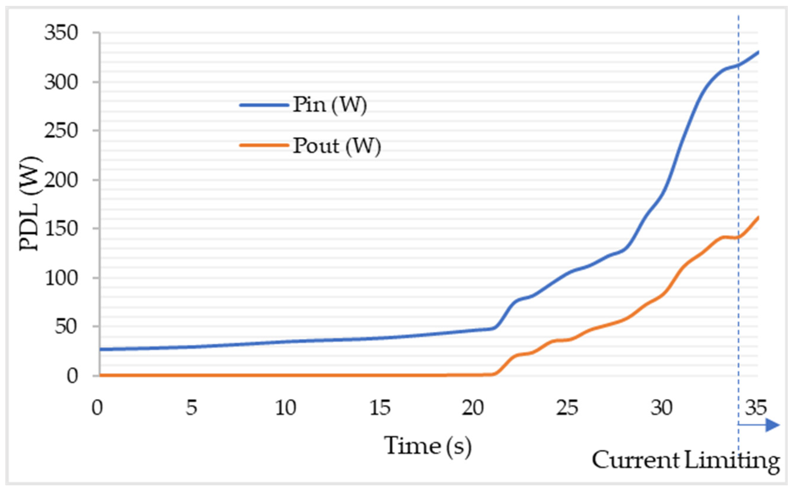
Figure 21 shows the PDL starting from the time we turned on the power supply until the time when the power supply reached its current limit of 3.5 A. It took about 21 s for PTU and PRU to form the perfect resonance. PDL became unstable after 21 s, which ramped up until the current limit of the DC power supply was reached. The instability phenomenon agreed with both the simulation results and the theory of NIC via sub-harmonic oscillation. Subharmonic oscillation successfully converted the low frequency current back into the transmitting coil as a current feedback to the closed-loop of the resonant WPT. Although the detailed physics still remain to be explored, the experimental result matched the simulation results for instability current surge. The current-limiting function was activated at 34 s, after that the voltage of the DC power supply dropped and the power output still increased for several seconds before it dropped down to 60% of the maximum PDL.
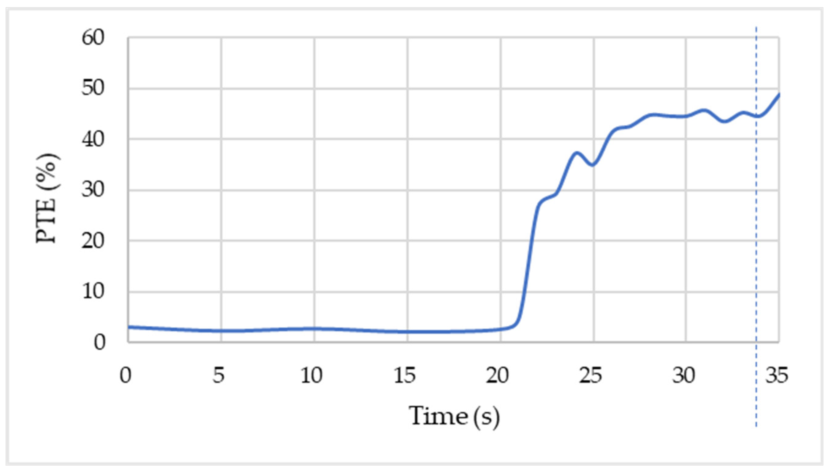
Figure 22 shows the PTE of the resonant WPT. The PTE grew simultaneously when the instability current was shown, which showed 50% efficiency in this experiment. In other experiments, a 65% PTE could be delivered with a lower battery voltage and lower PDL that extended the time the current was limited from the DC power supply. The PTE remained at 50% when the current limit was reached. PTE icreased simultaneously with the increased PDL, which favored a higher power transfer as more D-mode GaN HEMT transistors could be connected in parallel in the future.

5. Conclusions

This paper revealed a passive circuit that can be used as the PRU in resonant WPT for acquiring power from PTU. The experiment showed that 1 A of charging current flows into a 132 V battery string with a 150 W power transfer from 50 cm away, which is useful in EV charging. PRU consists of a voltage divider using the capacitors and an AC-DC converter using a pair of high voltage sources. PRU behaves like an NIC, which is formed by passive elements and needs no auxiliary power. A phenomenon is observed that when the PTU switching frequency matches the PRU resonance frequency—the phases of the PTU output current and the transmitting coil voltage and receiving coil voltage will self-organize to deliver high power in a negative damping resonance, which induces an instability current ramp and produces a high-power transfer. This instability current phenomenon shows a nonlinear effect due to different harmonics in which the current can yield different impedance features. In our experiment, the voltage from the DC power decreases its voltage without causing PTE degeneration; however, the PDL decreases. When the high-frequency AC source is implemented using the GaN HEMT transistor and class E circuit, the nonlinear behavior still persists. This depends on the constant current control of the specific DC power supply that is used when the current limit of the DC power supply is reached. In the future, we will perform research work on subharmonic oscillation theories to explore the possible control methods to regulate the PTU output current for sustaining WPT at a high PDL when this type of PRU is used. Furthermore, we will fabricate many more 20 mm D-mode GaN HEMT devices and integrate them together into a higher current switch for PTU in the future.

Author Contributions

Conceptualization, W.-H.C.; Methodology, D.U.; Validation, C.-Y.L., H.-C.T. and Y.-T.S.; Formal analysis, C.-Y.L. and C.-C.W.; Investigation, C.-Y.L., H.-C.T. and Y.-T.S.; Resources, E.-Y.C.; Writing—original draft, C.-C.W. and W.-H.C.; Writing—review & editing, C.-C.W. and D.U.; Visualization, W.-H.C.; Supervision, E.-Y.C.; Project administration, E.-Y.C.; Funding acquisition, W.-H.C. and E.-Y.C. All authors have read and agreed to the published version of the manuscript.

Funding

This research was funded by the National Science and Technology Council, R.O.C., grant number NSTC 112-2622-8-A49-013-SB, NSTC 112-2221-E-A49-073 -, and 110A0054TI. In part, this work was also financially supported by the “Center for the Semiconductor Technology Research” from The Featured Areas Research Center Program within the framework of the Higher Education Sprout Project by the Ministry of Education (MOE) in Taiwan.

Data Availability Statement

Data is contained within the article.

Acknowledgments

The authors also thank You-Chen Weng of the CSD Lab for fabricating the D-Mode MIS-HEMT chips and IMLab graduate students for their help in the experimental setup.

Conflicts of Interest

The authors declare no conflict of interest.

References

  1. Zhang, Z.; Pang, H.; Georgiadis, A.; Cecati, C. Wireless power transfer—An overview. IEEE Trans. Ind. Electron. 2018, 66, 1044–1058. [Google Scholar] [CrossRef]
  2. Wang, Y.; Sun, Z.; Guan, Y.; Xu, D. Overview of Megahertz Wireless Power Transfer. Proc. IEEE 2023, 111, 528–554. [Google Scholar] [CrossRef]
  3. Ahmad, A.; Alam, M.S.; Chabaan, R. A Comprehensive Review of Wireless Charging Technologies for Electric Vehicles. IEEE Trans. Transp. Electrif. 2018, 4, 38–63. [Google Scholar] [CrossRef]
  4. Yan, Y.; Shi, W.; Zhang, X. Design of UAV wireless power transmission system based on coupling coil structure optimization. EURASIP J. Wirel. Commun. Netw. 2020, 2020, 67. [Google Scholar] [CrossRef]
  5. Khan, S.R.; Pavuluri, S.K.; Cummins, G.; Desmulliez, M. Wireless Power Transfer Techniques for Implantable Medical Devices: A Review. Sensors 2020, 20, 3487. [Google Scholar] [CrossRef] [PubMed]
  6. Liu, C.-Y.; Wang, G.-B.; Wu, C.-C.; Chang, E.Y.; Cheng, S.; Chieng, W.-H. Derivation of the Resonance Mechanism for Wireless Power Transfer Using Class-E Amplifier. Energies 2021, 14, 632. [Google Scholar] [CrossRef]
  7. Paolucci, M.; Green, P.B. Benefits of GaN e-Mode HEMTs in Wireless Power Transfer—GaN Power Devices in Resonant Class D and Class E Radio Frequency Power Amplifiers. Rev 1.0. Infineon, White Paper. Available online: infineon.com (accessed on 1 October 2018).
  8. Choi, J.; Tsukiyama, D.; Tsuruda, Y.; Davila, J.M.R. High-frequency, high-power resonant inverter with eGaN FET for wireless power transfer. IEEE Trans. Power Electron. 2017, 33, 1890–1896. [Google Scholar] [CrossRef]
  9. Sinha, S.; Regensburger, B.; Kumar, A.; Afridi, K. A very-high-power-transfer-density GaN-based capacitive wireless power transfer system. In Proceedings of the 2017 IEEE 5th Workshop on Wide Bandgap Power Devices and Applications (WiPDA), Albuquerque, NM, USA, 30 October–1 November 2017; pp. 360–365. [Google Scholar]
  10. Abou Houran, M.; Yang, X.; Chen, W. Free Angular-Positioning Wireless Power Transfer Using a Spherical Joint. Energies 2018, 11, 3488. [Google Scholar] [CrossRef]
  11. Jolani, F.; Yu, Y.-Q.; Chen, Z. A planar positioning-free magnetically-coupled resonant wireless power transfer. In Proceedings of the 2015 IEEE Wireless Power Transfer Conference (WPTC), Boulder, CO, USA, 13–15 May 2015; pp. 1–3. [Google Scholar] [CrossRef]
  12. Liu, C.-Y.; Wu, C.-C.; Tang, L.-C.; Shieh, Y.-T.; Chieng, W.-H.; Chang, E.-Y. Resonant Mechanism for a Long-Distance Wireless Power Transfer Using Class E PA and GaN HEMT. Energies 2023, 16, 3657. [Google Scholar] [CrossRef]
  13. Li, J.; Qin, R.; Sun, J.; Costonett, D. Systematic Design of a 100-W 6.78-MHz Wireless Charging Station Covering Multiple Devices and a Large Charging Area. IEEE Trans. Power Electron. 2022, 37, 4877–4889. [Google Scholar] [CrossRef]
  14. Huang, X.; Yu, Z.; Dou, Y.; Lin, S.; Ouyang, Z.; Andersen, M.A.E. Load-Independent Push–Pull Class E 2 Topology with Coupled Inductors for MHz-WPT Applications. IEEE Trans. Power Electron. 2022, 37, 8726–8737. [Google Scholar] [CrossRef]
  15. Liu, J.; Liu, Z.; Chen, W.; Sun, Z.; Su, H. An Optimized Coil Array and Passivity-Based Control for Receiving Side Multilevel Connected DC-DC Converter of Dynamic Wireless Charging. IEEE Trans. Veh. Technol. 2022, 71, 3715–3726. [Google Scholar] [CrossRef]
  16. Hou, X.; Hu, H.; Su, Y.; Liu, Z.; Deng, Z.; Deng, R. A Multirelay Wireless Power Transfer System With Double-Sided LCC Compensation Network for Online Monitoring Equipment. IEEE J. Emerg. Sel. Top. Power Electron. 2022, 11, 1262–1271. [Google Scholar] [CrossRef]
  17. Li, J.; Wang, C.; Wang, L.; Ding, Y.; Yu, T.; Cheng, Y. A comparative study on transmission performance of multistage wireless power transfer systems using SPS compensation and LCC compensation. Int. J. Circuit Theory Appl. 2022, 51, 1625–1641. [Google Scholar] [CrossRef]
  18. Larky, A. Negative-impedance converters. IRE Trans. Circuit Theory 1957, 4, 124–131. [Google Scholar] [CrossRef]
  19. Yoon, S.H.; Kim, T.H.; Yook, J.G.; Yun, G.H.; Lee, W.Y. High Q-factor WPT system with negative impedance converter. In Proceedings of the 2017 IEEE Wireless Power Transfer Conference (WPTC), Taipei, Taiwan, 10–12 May 2017; pp. 1–4. [Google Scholar]
  20. Kim, T.H.; Yun, G.H.; Lee, W.; Yook, J.G. Highly efficient WPT system with negative impedance converter for Q-factor improvement. IEEE Access 2019, 7, 108750–108760. [Google Scholar] [CrossRef]
  21. Abramov, E.; Schultz, Y.; Evzelman, M.; Peretz, M.M. Analysis and design of post-regulation stages for resonant capacitively-coupled wireless power systems. In Proceedings of the 2022 IEEE Applied Power Electronics Conference and Exposition (APEC), Houston, TX, USA, 20–24 March 2022; pp. 492–499. [Google Scholar]
  22. Harmonic and Subharmonic Oscillations. Available online: https://phys.libretexts.org/bookshelves/classical_mechanics/essential_graduate_physics_-_classical_mechanics_(likharev)/05%3a_oscillations/5.08%3a_harmonic_and_subharmonic_oscillations (accessed on 17 September 2023).
  23. Hayashi, C. Subharmonic oscillations in nonlinear systems. J. Appl. Phys. 1953, 24, 521–529. [Google Scholar] [CrossRef]
  24. Weng, Y.-C.; Wu, C.-C.; Chang, E.Y.; Chieng, W.-H. Minimum Power Input Control for Class-E Amplifier Using Depletion-Mode Gallium Nitride High Electron Mobility Transistor. Energies 2021, 14, 2302. [Google Scholar] [CrossRef]
  25. Ke, C.-Y.; Wang, W.-C.; Ker, M.-D.; Yang, C.-Y.; Chang, E.Y. Investigation on ESD robustness of 1200-V D- mode GaN MIS-HEMTs with HBM ESD test and TLP measurement. In Proceedings of the 2023 International VLSI Symposium on Technology, Systems and Applications (VLSI-TSA/VLSI-DAT), Hsinchu, Taiwan, 17–20 April 2023; pp. 1–2. [Google Scholar] [CrossRef]
  26. Preuss, V.H.B. A Software Package for the Steady-State Simulation of Autonomous Circuits Using the Harmonic Balance Method. Master’s Thesis, Federal University of Santa Catarina, Florianópolis, Brazil, 2021. [Google Scholar]
  27. Keysight PathWave Advanced Design System (ADS), Chapter 3 Harmonic Balance (HB) Simulation. Available online: https://www.keysight.com/us/en/products/software/pathwave-design-software/pathwave-advanced-design-system.html (accessed on 17 November 2023).
  28. Donati Guerrieri, S.; Ramella, C.; Catoggio, E.; Bonani, F. Bridging the Gap between Physical and Circuit Analysis for Variability-Aware Microwave Design: Modeling Approaches. Electronics 2022, 11, 860. [Google Scholar] [CrossRef]
  29. Shieh, Y.-T.; Wu, C.-C.; Liu, C.-Y.; Chieng, W.-H.; Su, Y.-S.; Jeng, S.-L.; Chang, E.-Y. Lithium Battery Model and Its Application to Parallel Charging. Energies 2022, 15, 4767. [Google Scholar] [CrossRef]
Figure 1. PTU using class E amplifier [24].
Energies 16 07856 g001
Figure 2. The illustration of (a) drain voltage vx, (b) phase angle ϕ and (c) phase angle β.
Energies 16 07856 g002
Figure 3. Configuration of the proposed PRU.
Energies 16 07856 g003
Figure 4. Transformer circuit model for WPT.
Energies 16 07856 g004
Figure 5. Characteristics of the D-mode GaN HEMT used this work: (a) ID-VD curve and (b) C-VD curve.
Energies 16 07856 g005
Figure 6. (a) The equivalent AC-DC converter circuit in PRU and (b) its ideal waveforms.
Energies 16 07856 g006
Figure 7. The capacitive voltage divider circuit in PRU.
Energies 16 07856 g007
Figure 8. The flat-band band-pass filter circuit (a) without a stabilization capacitor and (b) with a stabilization capacitor C a .
Energies 16 07856 g008
Figure 9. The admittance transfer function of the flat-band band-pass filter.
Energies 16 07856 g009
Figure 10. The equivalent circuit of the resonant WPT for battery charging.
Energies 16 07856 g010
Figure 11. Coupling coefficient vs. distance of power transfer.
Energies 16 07856 g011
Figure 12. The voltage gain in terms of the coupling coefficient for different load resistances Zo when CT = 200 pF and L2 = 7 uH.
Energies 16 07856 g012
Figure 13. PSpice Simulation: (a) simulation circuit of the proposed PRU, (b) resonance results with a PRU in the WPT application, and (c) phase changes during the resonance formation.
Energies 16 07856 g013
Figure 14. (a) PSpice simulation for resonant WPT using a class E amplifier in PTU, (b) its results with a stable output current iB to the battery (pink color), the input current of PTU iL1 (purple color) and the output voltage across the battery (green color), and (c) the class E PA responses for resonant WPT.
Energies 16 07856 g014aEnergies 16 07856 g014b
Figure 15. The instability current with a class E amplifier used in PTU including the input current of the PTU (blue color) and the output current to the battery (red color).
Energies 16 07856 g015
Figure 16. Numerical results of PDL and PTE via different battery voltages.
Energies 16 07856 g016
Figure 17. The experiment setup of the resonant WPT system.
Energies 16 07856 g017
Figure 18. Wave forms of voltage and current from the oscilloscope, including PTU V G S (dark blue color), PTU V D S (cyan color), PRU I B (purple color), PRU V B (green color), and calculated power transfer (red color).
Energies 16 07856 g018
Figure 19. Comparison of (a) oscilloscope snapshot data VDS and VGS and (b) simulation export data VDS and VGS.
Energies 16 07856 g019
Figure 20. FFT of the battery voltage response in WPT charging.
Energies 16 07856 g020
Figure 21. The historical trend of input and output power from one experiment.
Energies 16 07856 g021
Figure 22. The historical trend of PTE calculations from the experiment.
Energies 16 07856 g022
Table 1. The 20 mm D-mode GaN HEMT parameters.
SymbolDescriptionUnitVDS
0 V600 V
CossOutput capacitancepF3117
CissInput capacitancepF4631
CrssFeedback capacitancepF238
VthGate turn on voltageV−9
VGSMaximumV10~−30
RDS,onOn resistance m Ω 900
VBDBreakdown voltageV600
iD,cont.Continuous drain currentA3
Table 2. List of parameters in simulation 1.
ItemDescriptionUnitValue
R T PTU coil resistanceΩ0.1
R R PRU coil resistanceΩ0.1
R B Battery resistanceΩ0.1
L R Leakage inductance of WPT transformeruH5
L M Magnetization inductance of WPT transformeruH0.1
L B Band pass filter inductanceuH2
D 1 , 2 , 3 High voltage, fast recovery diode; SiCSTPSC406D
C r PRU resonance capacitancepF290
C P PRU AC voltage divider capacitancenF5
C B Battery capacitanceF2000
C c PRU AC-DC output capacitanceuF1
C a PRU stabilization capacitancemF1
kMagnetic coupling coefficient 1
V B Battery voltageV4
Disclaimer/Publisher’s Note: The statements, opinions and data contained in all publications are solely those of the individual author(s) and contributor(s) and not of MDPI and/or the editor(s). MDPI and/or the editor(s) disclaim responsibility for any injury to people or property resulting from any ideas, methods, instructions or products referred to in the content.